EP2120247A2 - Dispositif émetteur d'électrons et appareil d'affichage d'images - Google Patents
Dispositif émetteur d'électrons et appareil d'affichage d'images Download PDFInfo
- Publication number
- EP2120247A2 EP2120247A2 EP09160122A EP09160122A EP2120247A2 EP 2120247 A2 EP2120247 A2 EP 2120247A2 EP 09160122 A EP09160122 A EP 09160122A EP 09160122 A EP09160122 A EP 09160122A EP 2120247 A2 EP2120247 A2 EP 2120247A2
- Authority
- EP
- European Patent Office
- Prior art keywords
- electron
- activation
- film
- layer
- suppressing layer
- Prior art date
- Legal status (The legal status is an assumption and is not a legal conclusion. Google has not performed a legal analysis and makes no representation as to the accuracy of the status listed.)
- Granted
Links
- 230000004913 activation Effects 0.000 claims abstract description 101
- 239000010408 film Substances 0.000 claims abstract description 72
- 239000000758 substrate Substances 0.000 claims abstract description 39
- 239000012789 electroconductive film Substances 0.000 claims abstract description 37
- OKTJSMMVPCPJKN-UHFFFAOYSA-N Carbon Chemical compound [C] OKTJSMMVPCPJKN-UHFFFAOYSA-N 0.000 claims abstract description 26
- QJGQUHMNIGDVPM-UHFFFAOYSA-N nitrogen group Chemical group [N] QJGQUHMNIGDVPM-UHFFFAOYSA-N 0.000 claims abstract description 24
- 229910052799 carbon Inorganic materials 0.000 claims abstract description 22
- VYPSYNLAJGMNEJ-UHFFFAOYSA-N Silicium dioxide Chemical compound O=[Si]=O VYPSYNLAJGMNEJ-UHFFFAOYSA-N 0.000 claims description 27
- IJGRMHOSHXDMSA-UHFFFAOYSA-N Atomic nitrogen Chemical compound N#N IJGRMHOSHXDMSA-UHFFFAOYSA-N 0.000 claims description 19
- 239000011521 glass Substances 0.000 claims description 12
- 229910052581 Si3N4 Inorganic materials 0.000 claims description 10
- HQVNEWCFYHHQES-UHFFFAOYSA-N silicon nitride Chemical compound N12[Si]34N5[Si]62N3[Si]51N64 HQVNEWCFYHHQES-UHFFFAOYSA-N 0.000 claims description 10
- 229910052757 nitrogen Inorganic materials 0.000 claims description 9
- 229910052681 coesite Inorganic materials 0.000 claims description 8
- 229910052906 cristobalite Inorganic materials 0.000 claims description 8
- 239000000377 silicon dioxide Substances 0.000 claims description 8
- 229910052682 stishovite Inorganic materials 0.000 claims description 8
- 229910052905 tridymite Inorganic materials 0.000 claims description 8
- PMHQVHHXPFUNSP-UHFFFAOYSA-M copper(1+);methylsulfanylmethane;bromide Chemical compound Br[Cu].CSC PMHQVHHXPFUNSP-UHFFFAOYSA-M 0.000 claims description 5
- MZLGASXMSKOWSE-UHFFFAOYSA-N tantalum nitride Chemical compound [Ta]#N MZLGASXMSKOWSE-UHFFFAOYSA-N 0.000 claims description 4
- 239000010410 layer Substances 0.000 description 89
- 238000000034 method Methods 0.000 description 45
- 238000000151 deposition Methods 0.000 description 20
- 230000008569 process Effects 0.000 description 16
- CSCPPACGZOOCGX-UHFFFAOYSA-N Acetone Chemical compound CC(C)=O CSCPPACGZOOCGX-UHFFFAOYSA-N 0.000 description 15
- 239000010419 fine particle Substances 0.000 description 15
- OAICVXFJPJFONN-UHFFFAOYSA-N Phosphorus Chemical compound [P] OAICVXFJPJFONN-UHFFFAOYSA-N 0.000 description 14
- 239000000463 material Substances 0.000 description 14
- 229910052751 metal Inorganic materials 0.000 description 13
- 239000002184 metal Substances 0.000 description 13
- 238000007738 vacuum evaporation Methods 0.000 description 13
- 239000000126 substance Substances 0.000 description 11
- 238000010276 construction Methods 0.000 description 10
- 229920002120 photoresistant polymer Polymers 0.000 description 10
- 229910052814 silicon oxide Inorganic materials 0.000 description 10
- 230000003213 activating effect Effects 0.000 description 9
- 230000008021 deposition Effects 0.000 description 9
- 238000010586 diagram Methods 0.000 description 9
- 238000010438 heat treatment Methods 0.000 description 7
- 150000001722 carbon compounds Chemical class 0.000 description 6
- 239000007789 gas Substances 0.000 description 6
- 238000002156 mixing Methods 0.000 description 6
- 238000004544 sputter deposition Methods 0.000 description 6
- 239000002245 particle Substances 0.000 description 5
- 239000005361 soda-lime glass Substances 0.000 description 5
- 108010083687 Ion Pumps Proteins 0.000 description 4
- ISWSIDIOOBJBQZ-UHFFFAOYSA-N Phenol Chemical compound OC1=CC=CC=C1 ISWSIDIOOBJBQZ-UHFFFAOYSA-N 0.000 description 4
- QVGXLLKOCUKJST-UHFFFAOYSA-N atomic oxygen Chemical compound [O] QVGXLLKOCUKJST-UHFFFAOYSA-N 0.000 description 4
- 230000007423 decrease Effects 0.000 description 4
- 229910002804 graphite Inorganic materials 0.000 description 4
- 239000010439 graphite Substances 0.000 description 4
- 239000011229 interlayer Substances 0.000 description 4
- 239000001301 oxygen Substances 0.000 description 4
- 229910052760 oxygen Inorganic materials 0.000 description 4
- ZWEHNKRNPOVVGH-UHFFFAOYSA-N 2-Butanone Chemical compound CCC(C)=O ZWEHNKRNPOVVGH-UHFFFAOYSA-N 0.000 description 3
- QTBSBXVTEAMEQO-UHFFFAOYSA-N Acetic acid Chemical compound CC(O)=O QTBSBXVTEAMEQO-UHFFFAOYSA-N 0.000 description 3
- UHOVQNZJYSORNB-UHFFFAOYSA-N Benzene Chemical compound C1=CC=CC=C1 UHOVQNZJYSORNB-UHFFFAOYSA-N 0.000 description 3
- LFQSCWFLJHTTHZ-UHFFFAOYSA-N Ethanol Chemical compound CCO LFQSCWFLJHTTHZ-UHFFFAOYSA-N 0.000 description 3
- OKKJLVBELUTLKV-UHFFFAOYSA-N Methanol Chemical compound OC OKKJLVBELUTLKV-UHFFFAOYSA-N 0.000 description 3
- YXFVVABEGXRONW-UHFFFAOYSA-N Toluene Chemical compound CC1=CC=CC=C1 YXFVVABEGXRONW-UHFFFAOYSA-N 0.000 description 3
- 229910003481 amorphous carbon Inorganic materials 0.000 description 3
- 238000000576 coating method Methods 0.000 description 3
- 239000004020 conductor Substances 0.000 description 3
- 239000013078 crystal Substances 0.000 description 3
- 239000011159 matrix material Substances 0.000 description 3
- 239000000203 mixture Substances 0.000 description 3
- 239000003921 oil Substances 0.000 description 3
- 239000003960 organic solvent Substances 0.000 description 3
- 238000001552 radio frequency sputter deposition Methods 0.000 description 3
- 230000000087 stabilizing effect Effects 0.000 description 3
- QUSNBJAOOMFDIB-UHFFFAOYSA-N Ethylamine Chemical compound CCN QUSNBJAOOMFDIB-UHFFFAOYSA-N 0.000 description 2
- BAVYZALUXZFZLV-UHFFFAOYSA-N Methylamine Chemical compound NC BAVYZALUXZFZLV-UHFFFAOYSA-N 0.000 description 2
- ATUOYWHBWRKTHZ-UHFFFAOYSA-N Propane Chemical compound CCC ATUOYWHBWRKTHZ-UHFFFAOYSA-N 0.000 description 2
- 238000010521 absorption reaction Methods 0.000 description 2
- 150000001412 amines Chemical class 0.000 description 2
- ULDHMXUKGWMISQ-UHFFFAOYSA-N carvone Chemical compound CC(=C)C1CC=C(C)C(=O)C1 ULDHMXUKGWMISQ-UHFFFAOYSA-N 0.000 description 2
- 229910052804 chromium Inorganic materials 0.000 description 2
- 229910052802 copper Inorganic materials 0.000 description 2
- XBDQKXXYIPTUBI-UHFFFAOYSA-N dimethylselenoniopropionate Natural products CCC(O)=O XBDQKXXYIPTUBI-UHFFFAOYSA-N 0.000 description 2
- 238000005530 etching Methods 0.000 description 2
- 238000001704 evaporation Methods 0.000 description 2
- 230000008020 evaporation Effects 0.000 description 2
- 229910052737 gold Inorganic materials 0.000 description 2
- 239000011810 insulating material Substances 0.000 description 2
- VNWKTOKETHGBQD-UHFFFAOYSA-N methane Chemical compound C VNWKTOKETHGBQD-UHFFFAOYSA-N 0.000 description 2
- BDAGIHXWWSANSR-UHFFFAOYSA-N methanoic acid Natural products OC=O BDAGIHXWWSANSR-UHFFFAOYSA-N 0.000 description 2
- 150000004767 nitrides Chemical class 0.000 description 2
- 229910052763 palladium Inorganic materials 0.000 description 2
- 238000000206 photolithography Methods 0.000 description 2
- 238000001020 plasma etching Methods 0.000 description 2
- 229910052697 platinum Inorganic materials 0.000 description 2
- WOCIAKWEIIZHES-UHFFFAOYSA-N ruthenium(iv) oxide Chemical compound O=[Ru]=O WOCIAKWEIIZHES-UHFFFAOYSA-N 0.000 description 2
- 239000004065 semiconductor Substances 0.000 description 2
- 230000006641 stabilisation Effects 0.000 description 2
- 238000011105 stabilization Methods 0.000 description 2
- 239000010409 thin film Substances 0.000 description 2
- 229910052718 tin Inorganic materials 0.000 description 2
- XOLBLPGZBRYERU-UHFFFAOYSA-N tin dioxide Chemical compound O=[Sn]=O XOLBLPGZBRYERU-UHFFFAOYSA-N 0.000 description 2
- 229910052719 titanium Inorganic materials 0.000 description 2
- 229910052721 tungsten Inorganic materials 0.000 description 2
- GNFTZDOKVXKIBK-UHFFFAOYSA-N 3-(2-methoxyethoxy)benzohydrazide Chemical compound COCCOC1=CC=CC(C(=O)NN)=C1 GNFTZDOKVXKIBK-UHFFFAOYSA-N 0.000 description 1
- OSWFIVFLDKOXQC-UHFFFAOYSA-N 4-(3-methoxyphenyl)aniline Chemical compound COC1=CC=CC(C=2C=CC(N)=CC=2)=C1 OSWFIVFLDKOXQC-UHFFFAOYSA-N 0.000 description 1
- LSNNMFCWUKXFEE-UHFFFAOYSA-M Bisulfite Chemical compound OS([O-])=O LSNNMFCWUKXFEE-UHFFFAOYSA-M 0.000 description 1
- FGUUSXIOTUKUDN-IBGZPJMESA-N C1(=CC=CC=C1)N1C2=C(NC([C@H](C1)NC=1OC(=NN=1)C1=CC=CC=C1)=O)C=CC=C2 Chemical compound C1(=CC=CC=C1)N1C2=C(NC([C@H](C1)NC=1OC(=NN=1)C1=CC=CC=C1)=O)C=CC=C2 FGUUSXIOTUKUDN-IBGZPJMESA-N 0.000 description 1
- 239000005973 Carvone Substances 0.000 description 1
- OTMSDBZUPAUEDD-UHFFFAOYSA-N Ethane Chemical compound CC OTMSDBZUPAUEDD-UHFFFAOYSA-N 0.000 description 1
- VGGSQFUCUMXWEO-UHFFFAOYSA-N Ethene Chemical compound C=C VGGSQFUCUMXWEO-UHFFFAOYSA-N 0.000 description 1
- 239000005977 Ethylene Substances 0.000 description 1
- 229910003862 HfB2 Inorganic materials 0.000 description 1
- 102000006391 Ion Pumps Human genes 0.000 description 1
- 229910025794 LaB6 Inorganic materials 0.000 description 1
- 229910002674 PdO Inorganic materials 0.000 description 1
- -1 TiN Chemical class 0.000 description 1
- ATJFFYVFTNAWJD-UHFFFAOYSA-N Tin Chemical compound [Sn] ATJFFYVFTNAWJD-UHFFFAOYSA-N 0.000 description 1
- 229910007948 ZrB2 Inorganic materials 0.000 description 1
- IKHGUXGNUITLKF-XPULMUKRSA-N acetaldehyde Chemical compound [14CH]([14CH3])=O IKHGUXGNUITLKF-XPULMUKRSA-N 0.000 description 1
- 235000011054 acetic acid Nutrition 0.000 description 1
- 150000001298 alcohols Chemical class 0.000 description 1
- 150000001299 aldehydes Chemical class 0.000 description 1
- 150000001335 aliphatic alkanes Chemical class 0.000 description 1
- 150000001338 aliphatic hydrocarbons Chemical class 0.000 description 1
- 150000001336 alkenes Chemical class 0.000 description 1
- 150000001345 alkine derivatives Chemical class 0.000 description 1
- 229910045601 alloy Inorganic materials 0.000 description 1
- 239000000956 alloy Substances 0.000 description 1
- 229910052782 aluminium Inorganic materials 0.000 description 1
- PNEYBMLMFCGWSK-UHFFFAOYSA-N aluminium oxide Inorganic materials [O-2].[O-2].[O-2].[Al+3].[Al+3] PNEYBMLMFCGWSK-UHFFFAOYSA-N 0.000 description 1
- 239000003708 ampul Substances 0.000 description 1
- ADCOVFLJGNWWNZ-UHFFFAOYSA-N antimony trioxide Inorganic materials O=[Sb]O[Sb]=O ADCOVFLJGNWWNZ-UHFFFAOYSA-N 0.000 description 1
- 150000004945 aromatic hydrocarbons Chemical class 0.000 description 1
- VWZIXVXBCBBRGP-UHFFFAOYSA-N boron;zirconium Chemical compound B#[Zr]#B VWZIXVXBCBBRGP-UHFFFAOYSA-N 0.000 description 1
- 239000000919 ceramic Substances 0.000 description 1
- 230000008859 change Effects 0.000 description 1
- 238000005229 chemical vapour deposition Methods 0.000 description 1
- 239000011248 coating agent Substances 0.000 description 1
- 230000003247 decreasing effect Effects 0.000 description 1
- 239000003599 detergent Substances 0.000 description 1
- 230000006866 deterioration Effects 0.000 description 1
- 229910001873 dinitrogen Inorganic materials 0.000 description 1
- 238000007598 dipping method Methods 0.000 description 1
- 239000006185 dispersion Substances 0.000 description 1
- 230000000694 effects Effects 0.000 description 1
- 230000005684 electric field Effects 0.000 description 1
- 238000010894 electron beam technology Methods 0.000 description 1
- 235000019253 formic acid Nutrition 0.000 description 1
- 229910052732 germanium Inorganic materials 0.000 description 1
- 238000009499 grossing Methods 0.000 description 1
- 239000012535 impurity Substances 0.000 description 1
- 229910052738 indium Inorganic materials 0.000 description 1
- PJXISJQVUVHSOJ-UHFFFAOYSA-N indium(III) oxide Inorganic materials [O-2].[O-2].[O-2].[In+3].[In+3] PJXISJQVUVHSOJ-UHFFFAOYSA-N 0.000 description 1
- 229910052742 iron Inorganic materials 0.000 description 1
- 150000002576 ketones Chemical class 0.000 description 1
- YEXPOXQUZXUXJW-UHFFFAOYSA-N lead(II) oxide Inorganic materials [Pb]=O YEXPOXQUZXUXJW-UHFFFAOYSA-N 0.000 description 1
- 150000002736 metal compounds Chemical class 0.000 description 1
- 229910044991 metal oxide Inorganic materials 0.000 description 1
- 150000004706 metal oxides Chemical class 0.000 description 1
- WSFSSNUMVMOOMR-NJFSPNSNSA-N methanone Chemical compound O=[14CH2] WSFSSNUMVMOOMR-NJFSPNSNSA-N 0.000 description 1
- 238000012986 modification Methods 0.000 description 1
- 230000004048 modification Effects 0.000 description 1
- 229910052759 nickel Inorganic materials 0.000 description 1
- 150000007524 organic acids Chemical class 0.000 description 1
- 230000000704 physical effect Effects 0.000 description 1
- 238000005268 plasma chemical vapour deposition Methods 0.000 description 1
- 229910021420 polycrystalline silicon Inorganic materials 0.000 description 1
- 229920005591 polysilicon Polymers 0.000 description 1
- 239000001294 propane Substances 0.000 description 1
- 235000019260 propionic acid Nutrition 0.000 description 1
- QQONPFPTGQHPMA-UHFFFAOYSA-N propylene Natural products CC=C QQONPFPTGQHPMA-UHFFFAOYSA-N 0.000 description 1
- 125000004805 propylene group Chemical group [H]C([H])([H])C([H])([*:1])C([H])([H])[*:2] 0.000 description 1
- IUVKMZGDUIUOCP-BTNSXGMBSA-N quinbolone Chemical compound O([C@H]1CC[C@H]2[C@H]3[C@@H]([C@]4(C=CC(=O)C=C4CC3)C)CC[C@@]21C)C1=CCCC1 IUVKMZGDUIUOCP-BTNSXGMBSA-N 0.000 description 1
- 229930195734 saturated hydrocarbon Natural products 0.000 description 1
- 238000007789 sealing Methods 0.000 description 1
- 229910052710 silicon Inorganic materials 0.000 description 1
- 229910052709 silver Inorganic materials 0.000 description 1
- 238000007613 slurry method Methods 0.000 description 1
- 238000003980 solgel method Methods 0.000 description 1
- 125000006850 spacer group Chemical group 0.000 description 1
- 229910052715 tantalum Inorganic materials 0.000 description 1
- YEAUATLBSVJFOY-UHFFFAOYSA-N tetraantimony hexaoxide Chemical compound O1[Sb](O2)O[Sb]3O[Sb]1O[Sb]2O3 YEAUATLBSVJFOY-UHFFFAOYSA-N 0.000 description 1
- 229930195735 unsaturated hydrocarbon Natural products 0.000 description 1
- 239000012808 vapor phase Substances 0.000 description 1
- XLYOFNOQVPJJNP-UHFFFAOYSA-N water Substances O XLYOFNOQVPJJNP-UHFFFAOYSA-N 0.000 description 1
- 238000001039 wet etching Methods 0.000 description 1
- 229910052725 zinc Inorganic materials 0.000 description 1
Images


Classifications
-
- H—ELECTRICITY
- H01—ELECTRIC ELEMENTS
- H01J—ELECTRIC DISCHARGE TUBES OR DISCHARGE LAMPS
- H01J1/00—Details of electrodes, of magnetic control means, of screens, or of the mounting or spacing thereof, common to two or more basic types of discharge tubes or lamps
- H01J1/02—Main electrodes
- H01J1/30—Cold cathodes, e.g. field-emissive cathode
- H01J1/316—Cold cathodes, e.g. field-emissive cathode having an electric field parallel to the surface, e.g. thin film cathodes
-
- H—ELECTRICITY
- H01—ELECTRIC ELEMENTS
- H01J—ELECTRIC DISCHARGE TUBES OR DISCHARGE LAMPS
- H01J31/00—Cathode ray tubes; Electron beam tubes
- H01J31/08—Cathode ray tubes; Electron beam tubes having a screen on or from which an image or pattern is formed, picked up, converted, or stored
- H01J31/10—Image or pattern display tubes, i.e. having electrical input and optical output; Flying-spot tubes for scanning purposes
- H01J31/12—Image or pattern display tubes, i.e. having electrical input and optical output; Flying-spot tubes for scanning purposes with luminescent screen
- H01J31/123—Flat display tubes
- H01J31/125—Flat display tubes provided with control means permitting the electron beam to reach selected parts of the screen, e.g. digital selection
- H01J31/127—Flat display tubes provided with control means permitting the electron beam to reach selected parts of the screen, e.g. digital selection using large area or array sources, i.e. essentially a source for each pixel group
-
- H—ELECTRICITY
- H01—ELECTRIC ELEMENTS
- H01J—ELECTRIC DISCHARGE TUBES OR DISCHARGE LAMPS
- H01J2201/00—Electrodes common to discharge tubes
- H01J2201/30—Cold cathodes
- H01J2201/316—Cold cathodes having an electric field parallel to the surface thereof, e.g. thin film cathodes
- H01J2201/3165—Surface conduction emission type cathodes
-
- H—ELECTRICITY
- H01—ELECTRIC ELEMENTS
- H01J—ELECTRIC DISCHARGE TUBES OR DISCHARGE LAMPS
- H01J2329/00—Electron emission display panels, e.g. field emission display panels
- H01J2329/02—Electrodes other than control electrodes
- H01J2329/04—Cathode electrodes
- H01J2329/0486—Cold cathodes having an electric field parallel to the surface thereof, e.g. thin film cathodes
- H01J2329/0489—Surface conduction emission type cathodes
Definitions
- the present invention relates to an electron-emitting device and an image display apparatus using the electron-emitting devices.
- an electron-emitting device there is an electron-emitting device of a field emission type, a surface conduction type, or the like.
- a pair of device electrodes is formed onto an insulating substrate. Subsequently, the pair of device electrodes is connected through an electroconductive film.
- a process called "energization forming" for forming a first gap into a part of the electroconductive film is executed.
- the energization forming operation is a step of supplying a current to the electroconductive film and forming the first gap into a part of the electroconductive film by a Joule heat generated by the current. By the energization forming operation, a pair of electroconductive films which face through the first gap is formed.
- the activation operation is a process for applying a voltage between the pair of device electrodes in an atmosphere of a carbon-containing gas.
- electroconductive carbon films can be formed onto the substrate in the first gap and the electroconductive films near the first gap.
- the electron-emitting device is formed.
- an electric potential which is applied to one of the device electrodes is set to be higher than an electric potential which is applied to the other device electrode.
- a strong electric field is caused in a second gap. It is, consequently, considered that electrons tunnel from a number of portions (a plurality of electron-emitting regions) in a portion forming an outer edge of the second gap corresponding to an edge of the carbon film connected to the device electrode on the low potential side and a part of the electrons are emitted.
- the electron-emitting device As for the electron-emitting device, it is demanded to improve stable electron-emitting characteristics and an electron-emitting efficiency so that an image display apparatus using the electron-emitting devices can stably provide a bright display image.
- the efficiency used here is evaluated by a ratio of a current flowing between a pair of device electrodes of the surface conduction electron-emitting device (hereinbelow, referred to as a "device current”) when a voltage is applied between the device electrodes and a current which is emitted into a vacuum (hereinbelow, referred to as an "electron emission current"). Therefore, the electron-emitting device in which the device current is small and the emission current is large is demanded.
- the electron-emitting characteristics and efficiency which can be stably controlled are improved, for example, in an image display apparatus using phosphor as an image forming member, a high-quality image display apparatus which is bright at a low current such as a flat panel television can be realized. In association with the realization of the low current, costs of a driving circuit and the like constructing the image display apparatus can be also reduced.
- an emission current amount of the surface conduction electron-emitting device decreases contrarily.
- Initial emission currents of the respective electron-emitting devices are not substantially uniform and the devices show different activation characteristics due to such causes that a gas pressure during the activation differs depending on a location and the like. That is, when the activation is executed at the same time, the devices have a variation in efficiency. Therefore, in the case where the image display apparatus is constructed by using a plurality of surface conduction electron-emitting devices, there is such a problem that if the efficiencies of the electron-emitting devices are not uniform, the electron emission amount changes depending on the position of the device or a luminance fluctuation occurs.
- an image display apparatus using a plurality of such electron-emitting devices it is another object of the invention to provide an image display apparatus in which electron-emitting characteristics of the respective devices are uniform, a uniform luminance is obtained, and an excellent operation stability is obtained.
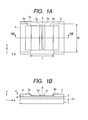
- FIGS. 1A and 1B are schematic diagrams illustrating a construction of an embodiment of an electron-emitting device of the invention.
- FIGS. 2A, 2B, 2C, and 2D are schematic diagrams illustrating producing steps of the electron-emitting device in FIGS. 1A and 1B .
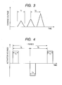
- FIG. 3 is a schematic diagram illustrating an example of a voltage waveform which is used in an energization forming operation of the electron-emitting device of the invention.
- FIG. 4 is a schematic diagram illustrating an example of a pulse voltage which is applied in an activating step of the electron-emitting device of the invention.
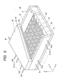
- FIG. 5 is a schematic diagram illustrating an example of a display panel of an image display apparatus using the electron-emitting devices of the invention.
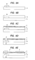
- FIGS. 6A, 6B, 6C, 6D, and 6E are schematic diagrams illustrating producing steps of the image display apparatus of the embodiment.
- FIGS. 7A, 7B, 7C, and 7D are schematic diagrams illustrating producing steps of the image display apparatus of the embodiment.
- an electron-emitting device comprising at least: a pair of device electrodes formed on a substrate; and an electroconductive film formed so as to connect the device electrodes, wherein the electroconductive film has a first gap between the device electrodes and has a carbon film having a second gap at least in the first gap, the substrate is constructed by stacking an activation suppressing layer containing nitrogen and an activation accelerating layer whose nitrogen containing ratio is smaller than that of the activation suppressing layer onto a base and has distribution of the nitrogen containing ratio in the activation suppressing layer in a film thickness direction, and the nitrogen containing ratio of the activation suppressing layer at the activation accelerating layer side is smaller than that at the base side.
- the electron-emitting device of the invention incorporates, as an exemplary embodiment, such a construction that the activation suppressing layer contains one of silicon nitride, aluminum nitride, and tantalum nitride and the activation accelerating layer is made of SiO 2 or glass containing SiO 2 as a main component.
- an image display apparatus in which a first substrate on which the plurality of electron-emitting devices of the invention are arranged and a second substrate on which image display members to which electrons emitted from the electron-emitting devices are irradiated are arranged in opposition to the electron-emitting devices are arranged so as to face each other.
- the nitrogen containing ratio of the activation suppressing layer to have the distribution in the film thickness direction, a progress of the activation is suppressed in the activation suppressing layer and the leakage current is reduced, so that the activation becomes uniform and the high-efficient electron-emitting device is obtained. Therefore, in the image display apparatus of the invention, a display of a uniform luminance having excellent operation stability can be performed at a low electric power consumption.
- the construction in which the activation suppressing layer and the activation accelerating layer are stacked onto the base is used as a substrate, further, the activation suppressing layer contains nitrogen, and the nitrogen containing ratio of the activation suppressing layer at the activation accelerating layer side is smaller than that at the base side.
- FIGS. 1A and 1B are diagrams illustrating the embodiment of an electron-emitting device to which the invention can be applied.
- FIG. 1A is a schematic plan view.
- FIG. 1B is a schematic cross sectional view taken along the line 1B-1B in FIG. 1A .
- FIGS. 2A to 2D are schematic cross sectional views illustrating producing steps of the electron-emitting device.
- a base 1 is illustrated.
- An activation suppressing layer 2 is formed on the base 1.
- An activation accelerating layer 3 is formed on the activation suppressing layer 2.
- Device electrodes 4 and 5 are formed on the activation accelerating layer 3.
- Electroconductive films 6a and 6b are arranged so as to face each other through a gap 9 (first gap).
- Carbon films 7a and 7b are arranged so as to face each other through a gap 8 (second gap).
- An insulating substrate 10 is constructed by stacking the activation suppressing layer 2 and the activation accelerating layer 3 onto the base 1.
- an insulating material such as quartz glass, glass in which a containing amount of impurities of Na or the like has been reduced, soda lime glass, ceramics such as alumina, Si substrate, or the like can be used as the base 1.
- the activation suppressing layer 2 which is used in the invention is an insulating layer containing nitrogen
- an insulating material obtained by mixing at least one kind of nitrides such as silicon nitride, aluminum nitride, and tantalum nitride into SiO 2 can be desirably used.
- the activation suppressing layer 2 has distribution of the nitrogen containing ratio in the film thickness direction.
- the layer 2 can have a construction in which the nitrogen containing ratio decreases continuously from the base 1 side toward the activation suppressing layer 2 side or a stacked construction of two or more layers in which the nitrogen containing ratio decreases step by step.
- the activation accelerating layer 3 is an insulating layer whose nitrogen containing ratio is smaller than that of the activation suppressing layer 2 and is, desirably, an insulating layer which does not contain nitrogen.
- SiO 2 or glass containing SiO 2 as a main component containing SiO 2 of 50 mass% or more is desirable.
- An ordinary thin film forming method can be adopted as a forming method of the activation suppressing layer 2 and the activation accelerating layer 3. That is, a vacuum evaporation depositing method, a sputtering method, a CVD method, a sol-gel method, or the like is used.
- a thickness of activation accelerating layer 3 is set to, desirably, 0.2 ⁇ m or less and, much desirably, 0.1 ⁇ m or less.
- the activation accelerating layer 3 is a layer in which the activation can be performed due to its existence and the activation suppressing layer 2 is a layer in which an activation speed is reduced due to such a layer.
- a general conductive material can be used as a material of the device electrodes 4 and 5 which face each other.
- a print conductor constructed by a metal such as Ni, Cr, Au, Mo, W, Pt, Ti, Al, Cu, or Pd or an alloy thereof, and a metal such as Pd, Ag, Au, RuO 2 , or Pd-Ag or a metal oxide thereof, and glass or the like can be used.
- a transparent conductor such as In 2 O 3 -SnO, a semiconductor material such as polysilicon, or the like can be also used.
- An interval L between the device electrodes 4 and 5 and a length W and a thickness d of each of them are designed in consideration of a form or the like which is applied.
- the interval L between the device electrodes can be set to a value within, desirably, a range from 500 nm to 500 ⁇ m, much desirably, a range from 5 ⁇ m to 50 ⁇ m in consideration of a voltage which is applied between the device electrodes or the like.
- the length W of each device electrode can be set to a value within a range from 5 ⁇ m to 500 ⁇ m in consideration of a resistance value and electron-emitting characteristics of the electrode.
- the thickness d of each of the device electrodes 4 and 5 can be set to a value within a range from 50 nm to 5 ⁇ m.
- each of the electroconductive films 6a and 6b is properly set in consideration of a step coverage to the device electrodes 4 and 5, a resistance value between the device electrodes 4 and 5, forming conditions, which will be described hereinafter, and the like.
- the film thickness is set to a value within, desirably, a range from 1 nm to hundreds of nm and, much desirably, a range from 1 nm to 50 nm.
- a metal such as Pd, Pt, Ru, Ag, Au, Ti, In, Cu, Cr, Fe, Zn, Sn, Ta, W, or Pb or an oxide such as PdO, SnO 2 , In 2 O 3 , PbO, or Sb 2 O 3 can be mentioned.
- a boride such as HfB 2 , ZrB 2 , LaB 6 , CeB 6 , YB 4 , or GdB 4 , a carbide such as TiC, ZrC, HfC, TaC, SiC, or WC, a nitride such as TiN, ZrN, or HfN, a semiconductor such as Si or Ge, carbon, or the like can be also mentioned.
- the fine particle film mentioned here is a film obtained by collecting a plurality of fine particles and its fine structure has a state where the fine particles are individually dispersed and arranged or a state where the fine particles are mutually neighboring or overlaid (also including a case where several fine particles are collected and an islandlike structure is formed as a whole).
- a particle size of fine particle lies within a range from 1 nm to 500 nm and, desirably, a range from 1 nm to 20 nm.
- the gap 9 between the electroconductive films 6a and 6b is a fissure having a high resistance formed in a part of a continuous electroconductive film 6 as will be described hereinafter, and depends on a film thickness, film quality, and a material of the electroconductive film 6, a method of an energization forming or the like, which will be described hereafter, and the like.
- electroconductive fine particles whose particle sizes lie within a range from 0.5 nm to 50 nm exist in the gap 9.
- the electroconductive fine particles contain a part or all of elements of the material constructing the electroconductive films 6a and 6b.
- Each of the carbon films 7a and 7b is a deposition film made of carbon and/or carbon compound which is deposited in portions around the gap 9 between the electroconductive films 6a and 6b in an activating step. There is also a case where the electroconductive films 6a and 6b are connected by an extremely small region.
- the base 1 is sufficiently cleaned by using a detergent, pure water, an organic solvent, and the like and the activation suppressing layer 2 and the activation accelerating layer 3 are deposited onto the surface of the base 1 by the vacuum evaporation depositing method, the sputtering method, or the like ( FIG. 2A ).
- the material of the device electrodes is deposited by the vacuum evaporation depositing method, the sputtering method, or the like and, thereafter, the device electrodes 4 and 5 are formed onto the substrate by using, for example, a photolithography technique ( FIG. 2B ).
- the substrate 10 formed with the device electrodes 4 and 5 is coated with an organic metal solution, thereby forming a thin organic metal film.
- an organic metal solution a solution of an organic metal compound containing the metal of the material of the electroconductive film 6 mentioned above as a main element can be used.
- the thin organic metal film is heat baking processed and patterned by a lift-off, etching, or the like, thereby forming the electroconductive film 6 ( FIG. 2C ).
- the forming method of the electroconductive film 6 is not limited to it but the vacuum evaporation depositing method, the sputtering method, a chemical vapor phase depositing method, a dispersion coating method, a dipping method, a spinner method, or the like can be also used.
- a forming step for forming the gap 9 into the electroconductive film 6 is executed.
- the gap 9 is formed into the electroconductive film 6 ( FIG. 2D ).
- a voltage waveform of the energization forming is illustrated in FIG. 3 .
- a pulse waveform is desirable as a voltage waveform.
- a process called an activating step is executed to the device obtained after the forming operation.
- the activating step is, for example, a process for repetitively applying the pulse voltage to the device under the atmosphere containing organic substance gases.
- the carbon films 7a and 7b made of carbon and/or carbon compound are deposited onto the device from the organic substances existing in the atmosphere, so that a device current If and an emission current Ie change remarkably.
- the activating step can be executed, for example, by repetitively applying a pulse under the atmosphere containing the organic substance gases in a manner similar to the energization forming.
- a proper organic substance an aliphatic hydrocarbon class of alkane, alkene, or alkyne, an aromatic hydrocarbon class, an alcohol class, an aldehyde class, a ketone class, an amine class, an organic acid class such as phenol, carvone, or sulfonic acid, or the like can be mentioned.
- saturated hydrocarbon expressed by a composition formula of C n H 2n+2 such as methane, ethane, or propane
- unsaturated hydrocarbon expressed by a composition formula of C n H 2n or the like such as ethylene or propylene
- Benzene, toluene, methanol, ethanol, formaldehyde, acetaldehyde, acetone, methyl ethyl ketone, methylamine, ethylamine, phenol, formic acid, acetic acid, propionic acid, or the like can be also used.
- carbon and/or carbon compound is graphite-like carbon.
- the graphite-like carbon in the invention contains the following carbon: carbon having a crystalline structure of perfect graphite (what is called HOPG); carbon in which a crystal particle size is equal to about 20 nm and a crystalline structure is slightly distorted (PG); carbon in which a crystal particle size is equal to about 2 nm and a crystalline structure is further distorted (GC); or amorphous carbon (which denotes amorphous carbon and/or a mixture of amorphous carbon and a fine crystal of the graphite).
- HOPG perfect graphite
- PG carbon in which a crystal particle size is equal to about 20 nm and a crystalline structure is slightly distorted
- GC carbon in which a crystal particle size is equal to about 2 nm and a crystalline structure is further distorted
- amorphous carbon which denotes amorphous carbon and/or a mixture of amorphous carbon and a fine crystal of the graphit
- the carbon compound can be desirably used. It is desirable that its film thickness is set to a value within a range of 50 nm or less and, much desirably, a range of 30 nm or less.
- the pulse voltage waveform which is used in the activating step is a waveform adapted to reverse a relation between an electric potential of the device electrode 4 or the electroconductive film 6a and an electric potential of the device electrode 5 or the electroconductive film 6b at predetermined timing or at a predetermined period (refer to FIG. 4 ).
- This step is a step of evacuating an organic substance in a vacuum chamber.
- a vacuum evacuating apparatus for evacuating the inside of the vacuum chamber it is desirable that an apparatus which does not use oil is used so that the oil generated from the apparatus does not exert an influence on characteristics of the device.
- a vacuum evacuating apparatus such as absorption pump, ion pump, or cryosorption pump can be mentioned.
- a partial pressure of the organic component in the vacuum chamber is set to, desirably, 1 ⁇ 10 -5 Pa or less and, particularly desirably, 1 ⁇ 10 -7 Pa or less as a partial pressure at which the carbon or carbon compound mentioned above is not almost newly deposited.
- heating conditions at this time it is desirable to execute the process at a temperature within a range from 80 to 400°C for a time as long as possible.
- the invention is not limited to those conditions but the above process is performed under conditions which are properly selected based on various conditions such as size and shape of the vacuum chamber, construction of the electron-emitting device, and the like. It is necessary to reduce a pressure in the vacuum chamber as low as possible to, desirably, 1 ⁇ 10 -5 Pa or less and, particularly desirably, 1 ⁇ 10 -6 Pa or less.
- the invention is not limited to it.
- the organic substance has sufficiently been removed, even if a vacuum degree itself decreases slightly, the sufficiently stable characteristics can be maintained.
- the deposition of the new carbon and/or carbon compound can be suppressed, so that the device current If and the emission current Ie are stabilized.
- the electron-emitting characteristics can be easily controlled according to an input signal.
- the invention can be applied to various fields such as electron source constructed by arranging a plurality of electron-emitting devices, image display apparatus, and the like.
- FIG. 5 illustrates an example of a display panel of the image display apparatus using the electron source constructed by arranging a plurality of electron-emitting devices 34 of the invention in a matrix form.
- FIG. 5 is a diagram schematically illustrating a construction of the display panel with a part cut away.
- An electron source substrate (first substrate) 31 is fixed onto a rear plate 41.
- a face plate (second substrate) 46 is constructed by forming a phosphor film (image display member) 44, a metal back 45, and the like onto an inner surface of a glass substrate 43.
- the rear plate 41 and the face plate 46 are connected to a supporting frame 42 by using frit glass or the like.
- An envelope 48 is constructed by being baked in, for example, the atmosphere or a nitrogen gas in a temperature range from 400 to 500°C for 10 minutes or longer and being seal-bonded.
- the envelope 48 is constructed by the face plate 46, supporting frame 42, and rear plate 41 as mentioned above. Since the rear plate 41 is provided mainly in order to enhance a strength of the substrate 31, if the substrate 31 itself has the enough strength, the rear plate 41 as a separate member can be made unnecessary. That is, the envelope 48 may be constructed by the face plate 46, supporting frame 42, and substrate 31 by directly seal-bonding the supporting frame 42 to the substrate 31.
- the envelope 48 having the enough strength against the atmospheric pressure can be also constructed by arranging a supporting member (not shown) called a spacer between the face plate 46 and the rear plate 41.
- the image display apparatus illustrated in FIG. 5 is manufactured, for example, as follows.
- the envelope 48 is evacuated through an exhaust pipe (not shown) by the evacuating apparatus which does not use any oil such as ion pump, absorption pump, turbo pump, or cryosorption pump while properly being heated.
- the evacuating apparatus which does not use any oil such as ion pump, absorption pump, turbo pump, or cryosorption pump while properly being heated.
- the inside of the envelope 48 was set into the atmosphere in which a vacuum degree is equal to about 10 -5 Pa and an amount of organic substance is sufficiently small, the envelope is sealed.
- a getter process can be also executed in order to maintain the vacuum degree after sealing the envelope 48.
- the getter process is such a process that just before or after the envelope 48 is/was sealed, a getter arranged at a predetermined position (not shown) in the envelope 48 is heated by heating using resistance heating, high-frequency heating, or the like, thereby forming an evaporation deposition film.
- the getter is ordinarily made of Ba or the like as a main component and maintains a vacuum degree in a range, for example, from 1 ⁇ 10 -5 to 1 ⁇ 10 -6 Pa by the adsorbing operation of the evaporation deposition film.
- the image display apparatus of the invention which can take such a construction, by applying a voltage to each electron-emitting device through terminals (out of the chamber) Dx 1 to Dx m connected to X-directional wirings 32 and terminals (out of the chamber) Dy 1 to Dy n connected to Y-directional wirings 33, an electron emission occurs.
- An electron beam is accelerated by applying a high voltage to the metal back 45 through a high-voltage terminal 47. The accelerated electron collides with the phosphor film 44, so that a light emission occurs and an image is formed.
- the image display apparatus of the invention can be used as a display apparatus of television broadcasting or a display apparatus of a television conference system, a computer, or the like.
- the 48 electron-emitting devices with the construction illustrated as an example in FIGS. 1A and 1B are arranged in one column onto one substrate. A producing process of the electron-emitting device will now be described with reference to FIGS. 2A to 2D .
- a film having a thickness of 0.4 ⁇ m obtained by mixing silicon nitride and silicon oxide is formed as an activation suppressing layer 2 onto cleaned soda lime glass by a sputtering method.
- the film is divisionally formed four times while changing a nitrogen containing ratio every thickness of 0.1 ⁇ m. Mole ratios of nitrogen and oxygen in the four layers of the activation suppressing layer are respectively set to 4:1, 3:2, 2:3, and 1:4 in stacking order.
- a silicon oxide film having a thickness of 0.05 ⁇ m is formed as an activation accelerating layer 3 by the sputtering method ( FIG. 2A ).
- a mask pattern of a photoresist (RD-2000N-41; manufactured by Hitachi Chemical Co., Ltd.) having opening portions corresponding to a pattern of electrodes is formed onto the substrate on which the activation accelerating layer 3 and the like have been formed.
- a Ti film having a thickness of 5 nm and a Pt film having a thickness of 100 nm are sequentially stacked by the vacuum evaporation depositing method.
- the photoresist is dissolved by an organic solvent and the Pt/Ti films on the photoresist are lifted off, thereby forming the device electrodes 4 and 5.
- An interval L between the device electrodes 4 and 5 is equal to 3 ⁇ m and an electrode width W is equal to 300 ⁇ m ( FIG. 2B ).
- a Cr film having a thickness of 100 nm is formed onto the device by the vacuum evaporation depositing method. Opening portions corresponding to a pattern of the electroconductive film 6 are formed by the photolithography technique and a Cr mask adapted to form the electroconductive film is formed.
- the Cr mask is coated with an organic Pd solution (ccp4230; manufactured by OKUNO CHEMICAL INDUSTRIES CO., LTD) by using a spinner and a baking process is executed in the atmosphere at 300°C for 10 minutes, thereby forming a fine particle film made by fine particles containing PdO as a main component.
- a thickness of this film is equal to 10 nm.
- the substrate 10 is set into the vacuum chamber.
- the inside of the vacuum chamber is evacuated so that a pressure reaches 1.3 ⁇ 10 -3 Pa.
- What is called an evacuating apparatus for a high vacuum constructed by a turbo pump and a rotary pump is used here as an evacuating apparatus.
- the evacuating apparatus further has an ion pump for a super-high vacuum besides those pumps and they can be properly switched and used.
- a pulse voltage is applied to each device and the forming operation is executed, thereby forming electron-emitting regions.
- a waveform of the pulse voltage which is used in this instance is a triangular wave pulse whose peak value is increased/decreased as illustrated in FIG. 3 .
- a resistance measuring pulse of 0.1V is inserted in a rest time of a forming pulse. When the resistance value exceeds 1 M ⁇ , the forming operation is finished.
- the peak value of the pulse at the end of the forming operation is equal to 5.0 to 5.1 V.
- a pressure in the vacuum chamber at this time is equal to 2.7 ⁇ 10 -4 Pa ( FIG. 2D ).
- a pulse illustrated in FIG. 4 is used as a pulse which is applied to the device.
- a pulse peak value Vact is equal to 10V at the beginning and is controlled so as to rise at a rate of 0.2 V/min and reach 18V.
- the stabilization operation is executed at 250°C for 12 hours in the vacuum of 10 -5 Pa.
- a triangular wave pulse of 5V is applied and a leakage current is measured, so that a mean value of the leakage currents of the 48 electron-emitting devices is equal to 3.1 ⁇ A.
- a triangular wave pulse of 16V is applied and electron-emitting characteristics are measured.
- the pressure in the vacuum chamber is equal to 1.3 ⁇ 10 -6 Pa, a distance between the anode electrode and the electron-emitting device is set to 4 mm, and an electric potential difference is set to 1 kV.
- a variation in emission currents of the 48 electron-emitting devices is equal to 4%.
- a silicon nitride film having a thickness of 0.4 ⁇ m is formed as an activation suppressing layer 2 onto the soda lime glass substrate. Thereafter, a silicon oxide film having a thickness of 0.05 ⁇ m is formed as an activation accelerating layer 3 onto the layer 2.
- Other producing steps are similar to those of Example 1 and an electron-emitting device is formed.
- a mean value of the leakage currents of the 48 electron-emitting devices is equal to 14.8 ⁇ A.
- the electron-emitting characteristics are measured by a method similar to that of Example 1, so that a variation in emission currents of the 48 electron-emitting devices is equal to 5%.
- 48 surface conduction electron-emitting devices are produced in a method similar to that of Example 1 except that a film obtained by mixing an aluminum nitride and a silicon oxide is deposited as an activation suppressing layer 2 by the vacuum evaporation depositing method.
- the film of the activation suppressing layer 2 is divisionally formed four times while changing the nitrogen containing ratio every thickness of 0.1 ⁇ m so that the thickness reaches 0.4 ⁇ m.
- Mole ratios of nitrogen and oxygen in the four layers of the activation suppressing layer 2 are respectively set to 4:1, 3:2, 2:3, and 1:4 in stacking order.
- a mean value of the leakage currents of the 48 electron-emitting devices is equal to 6.3 ⁇ A.
- Electron-emitting characteristics are measured by the same method as that of Example 1, so that a variation in emission currents of the 48 electron-emitting devices is equal to 5%.
- 48 surface conduction electron-emitting devices are produced in a method similar to that of Example 1 except that a film obtained by mixing a silicon nitride and a silicon oxide is deposited as an activation suppressing layer 2 by a plasma CVD method.
- a mean value of the leakage currents of the 48 electron-emitting devices is equal to 3.4 ⁇ A. Electron-emitting characteristics are measured by a method similar to that of Example 1, so that a variation in emission currents of the 48 electron-emitting devices is equal to 5%. As described above, according to results of Examples 1 to 3 having distribution in the nitrogen containing ratio of the activation suppressing layer 2 of the invention, the leakage current of the electron-emitting device is small as compared with the result of Comparison 1 which does not have distribution in the nitrogen containing ratio of the activation suppressing layer 2.
- a silicon nitride film having a thickness of 0.1 ⁇ m is formed as an activation suppressing layer 2 onto the soda lime glass substrate. Subsequently, a layer having a thickness of 0.3 ⁇ m obtained by mixing a silicon nitride and a silicon oxide so that a mole ratio of nitrogen and oxygen is equal to 1:1 is formed. Further, a silicon oxide film having a thickness of 0.05 ⁇ m is formed as an activation accelerating layer 3. Other producing steps are similar to those of Example 1 and 48 electron-emitting devices are formed. In this case, a mean value of the leakage currents of the 48 electron-emitting devices is equal to 8.9 ⁇ A. The electron-emitting characteristics are measured by a method similar to that of Example 1, so that a variation in emission currents of the 48 electron-emitting devices is equal to 5%.
- an electron source in which a plurality of surface conduction electron-emitting devices are arranged onto the substrate and wired in a matrix form and an image display apparatus using the electron source are produced by steps illustrated in FIGS. 6A to 6E and 7A to 7D .
- a Cr film having a thickness of 5 nm and an Au film having a thickness of 600 nm are sequentially stacked onto cleaned soda lime glass 71 by the vacuum evaporation depositing method. Thereafter, a surface of the stacked layers is spin-coated with a photoresist (AZ1370; manufactured by Hoechst Japan Ltd.) by a spinner. The photoresist is baked and, subsequently, a photomask image is exposed and developed, thereby forming a wiring pattern. The Au/Cr deposition films are wet-etched, thereby forming the X-directional wirings 32 of a desired shape ( FIG. 6A ).
- An interlayer insulating layer 72 made of a silicon oxide film having a thickness of 1.0 ⁇ m is deposited by an RF sputtering method ( FIG. 6B ).
- a film having a thickness of 0.4 ⁇ m obtained by mixing silicon nitride and silicon oxide is divisionally formed four times as an activation suppressing layer 2 onto the interlayer insulating layer 72 by the RF sputtering method while changing the nitrogen containing ratio every thickness of 0.1 ⁇ m. Mole ratios of nitrogen and oxygen in the four layers of the activation suppressing layer are respectively set to 4:1, 3:2, 2:3, and 1:4 in stacking order. Further, a silicon oxide film having a thickness of 0.05 ⁇ m is formed as an activation accelerating layer 3 by the RF sputtering method ( FIG. 6C ).
- a photoresist pattern to form a contact hole 73 into the activation accelerating layer 3, the activation suppressing layer 2 and the interlayer insulating layer 72 deposited in step-B and step-C is formed.
- the activation accelerating layer 3, the activation suppressing layer 2 and the interlayer insulating layer 72 is etched by using the photoresist pattern as a mask, thereby forming the contact hole 73.
- the etching is executed by an RIE (Reactive Ion Etching) method using CF 4 and H 2 gases ( FIG. 6D ).
- a pattern to form the device electrodes 4 and 5 is formed by a photoresist (RD-2000N-41; manufactured by Hitachi Chemical Co., Ltd.) and a Ti film having a thickness of 5 nm and an Ni film having a thickness of 100 nm are sequentially deposited by the vacuum evaporation depositing method.
- the photoresist pattern is dissolved by the organic solvent and the Ni/Ti deposition films are lifted off, thereby forming the device electrodes 4 and 5 in which the interval L between the device electrodes is equal to 3 ⁇ m and the width W is equal to 300 ⁇ m ( FIG. 6E ).
- a resist pattern is formed on portions other than the portion of the contact hole 73.
- a Ti film having a thickness of 5 nm and an Au film having a thickness of 500 nm are sequentially deposited by the vacuum evaporation deposition. The unnecessary portions are removed by the lift-off and the contact hole 73 is embedded ( FIG. 7A ).
- a photoresist pattern of the Y-directional wirings 33 is formed onto the device electrodes 4 and 5. After that, a Ti film having a thickness of 5 nm and an Au film having a thickness of 500 nm are sequentially deposited by the vacuum evaporation deposition. The unnecessary portions are removed by the lift-off and the Y-directional wirings 33 of a desired shape are formed ( FIG. 7B ).
- a Cr film 74 having a thickness of 30 nm is deposited by the vacuum evaporation deposition and patterned so as to have an opening portion of the shape of the electroconductive film 6. Subsequently, the surface is spin-coated with a Pd amine complex solution (ccp4230) by a spinner and a heat baking process is executed at 300°C for 12 minutes, thereby forming a PdO fine particle film 75.
- a thickness of film 75 is equal to 70 nm ( FIG. 7C ).
- the Cr film 74 is wet-etched by using an etchant and removed together with the unnecessary portion of the PdO fine particle film 75, thereby forming the electroconductive film 6 of a desired shape.
- the face plate 46 is arranged to a portion that is over the substrate 31 by 5 mm through the supporting frame 42. Subsequently, joint portions of the face plate 46, supporting frame 42, and rear plate 41 are coated with frit glass and they are baked in the atmosphere at 400°C for 10 minutes, thereby seal-bonding them. The substrate 31 is fixed to the rear plate 41 also by the frit glass.
- a stripe shape is used as a shape of a phosphor material of the face plate 46.
- black stripes are formed.
- gap portions among the black stripes are coated with color phosphor materials, thereby forming the phosphor film 44.
- a material containing graphite as a main component which is ordinarily often used is used as a material of the black stripes.
- a slurry method is used as a method of coating the glass substrate 43 with the phosphor material.
- a smoothing process (which is ordinarily called filming) is executed to the inner surface side of the phosphor film 44.
- the metal back 45 is formed by vacuum evaporation depositing an Al film.
- a transparent electrode (not shown) is provided on the outer surface side of the phosphor film 44 in order to further improve the conductivity of the phosphor film 44, in the embodiment, since the sufficient conductivity can be obtained only by the metal back 45, such a transparent electrode is omitted.
- the atmosphere in the glass chamber completed as mentioned above is evacuated to a vacuum degree of about 10 -4 Pa by a vacuum pump through the exhaust pipe (not shown).
- the Y-directional wirings 33 are coupled in common and the forming operation is executed every line. The forming is executed under the conditions used in Example 1.
- the exhaust pipe is connected to an ampoule filled with acetone serving as an activating substance. Acetone is introduced into the panel. The pressure is adjusted so that it reaches 1.3 ⁇ 10 -1 Pa. A rectangular wave pulse of 18V is applied. The pulse width is set to 100 ⁇ sec and the pulse interval is set to 20 msec.
- the activation operation is executed row by row.
- the Y-directional wirings 33 are coupled in common in a manner similar to step-K.
- a valve of a gas introducing apparatus is closed, the introduction of acetone is stopped, and the evacuation is continued for 5 hours while heating the whole glass panel to about 200°C. Subsequently, electrons are emitted by a passive matrix driving and the phosphor film 44 is allowed to perform the light emission from the whole surface. After confirming that the phosphor film 44 operated normally, the exhaust pipe is seal-bonded by heating and is fully sealed. After that, the getter (not shown) put in the panel is flashed by the high-frequency heating.
- the image display apparatus having a practically sufficient brightness can be produced and the leakage current at 5V of each electron-emitting device is suppressed to 7 ⁇ A or less.
- the luminance variation is equal to 12% or less.
- An electron-emitting device has a pair of device electrodes formed on a substrate and an electroconductive film connected to the device electrodes.
- the electroconductive film has a first gap between the device electrodes and has a carbon film having a second gap at least in the first gap.
- the substrate is formed by stacking a nitrogen-contained activation suppressing layer and an activation accelerating layer having a nitrogen containing ratio smaller than that of the activation suppressing layer onto a base and has nitrogen containing ratio distribution in the activation suppressing layer in a film thickness direction.
- the nitrogen containing ratio of the activation suppressing layer at the activation accelerating layer side is smaller than that at the base side.
Landscapes
- Cathode-Ray Tubes And Fluorescent Screens For Display (AREA)
- Cold Cathode And The Manufacture (AREA)
Applications Claiming Priority (1)
| Application Number | Priority Date | Filing Date | Title |
|---|---|---|---|
| JP2008126628A JP2009277459A (ja) | 2008-05-14 | 2008-05-14 | 電子放出素子及び画像表示装置 |
Publications (3)
| Publication Number | Publication Date |
|---|---|
| EP2120247A2 true EP2120247A2 (fr) | 2009-11-18 |
| EP2120247A3 EP2120247A3 (fr) | 2010-08-04 |
| EP2120247B1 EP2120247B1 (fr) | 2011-12-21 |
Family
ID=40793108
Family Applications (1)
| Application Number | Title | Priority Date | Filing Date |
|---|---|---|---|
| EP09160122A Not-in-force EP2120247B1 (fr) | 2008-05-14 | 2009-05-13 | Dispositif émetteur d'électrons et appareil d'affichage d'images |
Country Status (6)
| Country | Link |
|---|---|
| US (1) | US8013511B2 (fr) |
| EP (1) | EP2120247B1 (fr) |
| JP (1) | JP2009277459A (fr) |
| KR (1) | KR101055304B1 (fr) |
| CN (1) | CN101582358B (fr) |
| AT (1) | ATE538486T1 (fr) |
Families Citing this family (5)
| Publication number | Priority date | Publication date | Assignee | Title |
|---|---|---|---|---|
| EP2109132A3 (fr) * | 2008-04-10 | 2010-06-30 | Canon Kabushiki Kaisha | Appareil de faisceau à électrons et appareil d'affichage d'image l'utilisant |
| ATE531066T1 (de) | 2008-04-10 | 2011-11-15 | Canon Kk | Elektronenemitter sowie elektronenstrahlvorrichtung und bildanzeigevorrichtung mit diesem emitter |
| JP2009277457A (ja) * | 2008-05-14 | 2009-11-26 | Canon Inc | 電子放出素子及び画像表示装置 |
| JP2009277458A (ja) * | 2008-05-14 | 2009-11-26 | Canon Inc | 電子放出素子及び画像表示装置 |
| JP4458380B2 (ja) * | 2008-09-03 | 2010-04-28 | キヤノン株式会社 | 電子放出素子およびそれを用いた画像表示パネル、画像表示装置並びに情報表示装置 |
Citations (2)
| Publication number | Priority date | Publication date | Assignee | Title |
|---|---|---|---|---|
| JPH09293448A (ja) | 1996-04-25 | 1997-11-11 | Canon Inc | 電子放出素子及び電子源及び画像形成装置 |
| US20020084736A1 (en) | 1999-02-26 | 2002-07-04 | Masaaki Shibata | Electron-emitting device, electron source and image forming apparatus |
Family Cites Families (6)
| Publication number | Priority date | Publication date | Assignee | Title |
|---|---|---|---|---|
| EP0936651B1 (fr) * | 1998-02-12 | 2004-08-11 | Canon Kabushiki Kaisha | Procédé de fabrication d'un élément émetteur d'électrons. source d'électrons, et dispositif de formation d'images |
| US7230372B2 (en) * | 2004-04-23 | 2007-06-12 | Canon Kabushiki Kaisha | Electron-emitting device, electron source, image display apparatus, and their manufacturing method |
| JP3935479B2 (ja) * | 2004-06-23 | 2007-06-20 | キヤノン株式会社 | カーボンファイバーの製造方法及びそれを使用した電子放出素子の製造方法、電子デバイスの製造方法、画像表示装置の製造方法および、該画像表示装置を用いた情報表示再生装置 |
| JP4596878B2 (ja) * | 2004-10-14 | 2010-12-15 | キヤノン株式会社 | 構造体、電子放出素子、2次電池、電子源、画像表示装置、情報表示再生装置及びそれらの製造方法 |
| JP4946156B2 (ja) * | 2006-05-01 | 2012-06-06 | 富士ゼロックス株式会社 | 半導体膜及びその製造方法、並びに、該半導体膜を用いた受光素子、電子写真用感光体、プロセスカートリッジ、画像形成装置 |
| JP2008027853A (ja) * | 2006-07-25 | 2008-02-07 | Canon Inc | 電子放出素子、電子源および画像表示装置、並びに、それらの製造方法 |
-
2008
- 2008-05-14 JP JP2008126628A patent/JP2009277459A/ja not_active Withdrawn
-
2009
- 2009-05-11 US US12/463,715 patent/US8013511B2/en not_active Expired - Fee Related
- 2009-05-13 KR KR1020090041486A patent/KR101055304B1/ko not_active Expired - Fee Related
- 2009-05-13 AT AT09160122T patent/ATE538486T1/de active
- 2009-05-13 EP EP09160122A patent/EP2120247B1/fr not_active Not-in-force
- 2009-05-14 CN CN2009101408731A patent/CN101582358B/zh not_active Expired - Fee Related
Patent Citations (2)
| Publication number | Priority date | Publication date | Assignee | Title |
|---|---|---|---|---|
| JPH09293448A (ja) | 1996-04-25 | 1997-11-11 | Canon Inc | 電子放出素子及び電子源及び画像形成装置 |
| US20020084736A1 (en) | 1999-02-26 | 2002-07-04 | Masaaki Shibata | Electron-emitting device, electron source and image forming apparatus |
Also Published As
| Publication number | Publication date |
|---|---|
| EP2120247A3 (fr) | 2010-08-04 |
| US8013511B2 (en) | 2011-09-06 |
| JP2009277459A (ja) | 2009-11-26 |
| ATE538486T1 (de) | 2012-01-15 |
| US20090284127A1 (en) | 2009-11-19 |
| EP2120247B1 (fr) | 2011-12-21 |
| CN101582358A (zh) | 2009-11-18 |
| KR101055304B1 (ko) | 2011-08-09 |
| CN101582358B (zh) | 2012-01-25 |
| KR20090118864A (ko) | 2009-11-18 |
Similar Documents
| Publication | Publication Date | Title |
|---|---|---|
| US7582002B2 (en) | Manufacturing method of electron emitting device, electron source and image display apparatus | |
| JP4366235B2 (ja) | 電子放出素子、電子源及び画像表示装置の製造方法 | |
| US8013511B2 (en) | Highly-efficient electron-emitting device and image display apparatus having a substrate with a distribution of nitrogen containing ratio | |
| EP2120246A2 (fr) | Dispositif d'émission d'électrons et appareil d'affichage d'images | |
| JP2000195415A (ja) | 電子放出素子、電子源、画像形成装置及びそれらの製造方法 | |
| JP3689683B2 (ja) | 電子放出素子、電子源および画像形成装置の製造方法 | |
| JP3559689B2 (ja) | 電子放出素子、電子源、画像形成装置及びそれらの製造方法 | |
| JP3320363B2 (ja) | 電子放出素子、電子源、画像形成装置、及び電子放出素子の製造方法 | |
| JPH09293448A (ja) | 電子放出素子及び電子源及び画像形成装置 | |
| JP3428806B2 (ja) | 電子放出素子、電子源基板、および画像形成装置の製造方法 | |
| JP3241599B2 (ja) | 電子放出素子、電子源基板、電子源、表示パネルおよび画像形成装置の製造方法 | |
| JP3548431B2 (ja) | 電子源、該電子源を用いた画像形成装置 | |
| JPH10188854A (ja) | 画像形成装置及びその製造方法 | |
| JP2000195417A (ja) | 電子放出素子、電子源、画像形成装置及びそれらの製造方法 | |
| JP2000251795A (ja) | 画像形成装置 | |
| JP2000243232A (ja) | 電子放出素子、電子源基板および画像形成装置 | |
| JP2000021290A (ja) | 電子放出素子、電子源、画像形成装置及びそれらの製造方法 | |
| JP2000243236A (ja) | 電子放出素子、電子源基板及び画像形成装置 | |
| JP2000251689A (ja) | 電子放出素子の製造方法及びそれを用いた電子源基板、画像形成装置の製造方法及びその製造に用いる液滴付与装置 | |
| JP2000149770A (ja) | 表面伝導型電子放出素子、電子源、画像形成装置の製造方法 | |
| JPH09330652A (ja) | 電子放出素子の製造方法ならびに電子放出素子および画像形成装置 | |
| JP2000164117A (ja) | 電子放出素子、電子源、画像形成装置及びそれらの製造方法 | |
| JP2000251627A (ja) | 電子源基板及びそれを用いた画像形成装置 | |
| JP2004207124A (ja) | 電子放出素子の製造方法 | |
| JPH09223458A (ja) | 電子放出素子、電子源、および画像形成装置の製造方法 |
Legal Events
| Date | Code | Title | Description |
|---|---|---|---|
| PUAI | Public reference made under article 153(3) epc to a published international application that has entered the european phase |
Free format text: ORIGINAL CODE: 0009012 |
|
| AK | Designated contracting states |
Kind code of ref document: A2 Designated state(s): AT BE BG CH CY CZ DE DK EE ES FI FR GB GR HR HU IE IS IT LI LT LU LV MC MK MT NL NO PL PT RO SE SI SK TR |
|
| PUAL | Search report despatched |
Free format text: ORIGINAL CODE: 0009013 |
|
| AK | Designated contracting states |
Kind code of ref document: A3 Designated state(s): AT BE BG CH CY CZ DE DK EE ES FI FR GB GR HR HU IE IS IT LI LT LU LV MC MK MT NL NO PL PT RO SE SI SK TR |
|
| AX | Request for extension of the european patent |
Extension state: AL BA RS |
|
| RIC1 | Information provided on ipc code assigned before grant |
Ipc: H01J 31/12 20060101ALI20100625BHEP Ipc: H01J 1/316 20060101AFI20090702BHEP |
|
| 17P | Request for examination filed |
Effective date: 20110204 |
|
| GRAP | Despatch of communication of intention to grant a patent |
Free format text: ORIGINAL CODE: EPIDOSNIGR1 |
|
| RIC1 | Information provided on ipc code assigned before grant |
Ipc: H01J 31/12 20060101ALI20110302BHEP Ipc: H01J 1/316 20060101AFI20110302BHEP |
|
| RIN1 | Information on inventor provided before grant (corrected) |
Inventor name: TSUKAMOTO, TAKEO Inventor name: TAKEUCHI, EIJI |
|
| GRAS | Grant fee paid |
Free format text: ORIGINAL CODE: EPIDOSNIGR3 |
|
| 17Q | First examination report despatched |
Effective date: 20111007 |
|
| GRAA | (expected) grant |
Free format text: ORIGINAL CODE: 0009210 |
|
| AK | Designated contracting states |
Kind code of ref document: B1 Designated state(s): AT BE BG CH CY CZ DE DK EE ES FI FR GB GR HR HU IE IS IT LI LT LU LV MC MK MT NL NO PL PT RO SE SI SK TR |
|
| REG | Reference to a national code |
Ref country code: GB Ref legal event code: FG4D |
|
| REG | Reference to a national code |
Ref country code: CH Ref legal event code: EP |
|
| REG | Reference to a national code |
Ref country code: AT Ref legal event code: REF Ref document number: 538486 Country of ref document: AT Kind code of ref document: T Effective date: 20120115 |
|
| REG | Reference to a national code |
Ref country code: IE Ref legal event code: FG4D |
|
| REG | Reference to a national code |
Ref country code: DE Ref legal event code: R096 Ref document number: 602009004268 Country of ref document: DE Effective date: 20120322 |
|
| REG | Reference to a national code |
Ref country code: NL Ref legal event code: VDEP Effective date: 20111221 |
|
| PG25 | Lapsed in a contracting state [announced via postgrant information from national office to epo] |
Ref country code: NO Free format text: LAPSE BECAUSE OF FAILURE TO SUBMIT A TRANSLATION OF THE DESCRIPTION OR TO PAY THE FEE WITHIN THE PRESCRIBED TIME-LIMIT Effective date: 20120321 Ref country code: LT Free format text: LAPSE BECAUSE OF FAILURE TO SUBMIT A TRANSLATION OF THE DESCRIPTION OR TO PAY THE FEE WITHIN THE PRESCRIBED TIME-LIMIT Effective date: 20111221 |
|
| LTIE | Lt: invalidation of european patent or patent extension |
Effective date: 20111221 |
|
| PG25 | Lapsed in a contracting state [announced via postgrant information from national office to epo] |
Ref country code: SI Free format text: LAPSE BECAUSE OF FAILURE TO SUBMIT A TRANSLATION OF THE DESCRIPTION OR TO PAY THE FEE WITHIN THE PRESCRIBED TIME-LIMIT Effective date: 20111221 Ref country code: HR Free format text: LAPSE BECAUSE OF FAILURE TO SUBMIT A TRANSLATION OF THE DESCRIPTION OR TO PAY THE FEE WITHIN THE PRESCRIBED TIME-LIMIT Effective date: 20111221 Ref country code: GR Free format text: LAPSE BECAUSE OF FAILURE TO SUBMIT A TRANSLATION OF THE DESCRIPTION OR TO PAY THE FEE WITHIN THE PRESCRIBED TIME-LIMIT Effective date: 20120322 Ref country code: LV Free format text: LAPSE BECAUSE OF FAILURE TO SUBMIT A TRANSLATION OF THE DESCRIPTION OR TO PAY THE FEE WITHIN THE PRESCRIBED TIME-LIMIT Effective date: 20111221 Ref country code: SE Free format text: LAPSE BECAUSE OF FAILURE TO SUBMIT A TRANSLATION OF THE DESCRIPTION OR TO PAY THE FEE WITHIN THE PRESCRIBED TIME-LIMIT Effective date: 20111221 Ref country code: NL Free format text: LAPSE BECAUSE OF FAILURE TO SUBMIT A TRANSLATION OF THE DESCRIPTION OR TO PAY THE FEE WITHIN THE PRESCRIBED TIME-LIMIT Effective date: 20111221 |
|
| PG25 | Lapsed in a contracting state [announced via postgrant information from national office to epo] |
Ref country code: CY Free format text: LAPSE BECAUSE OF FAILURE TO SUBMIT A TRANSLATION OF THE DESCRIPTION OR TO PAY THE FEE WITHIN THE PRESCRIBED TIME-LIMIT Effective date: 20111221 Ref country code: BE Free format text: LAPSE BECAUSE OF FAILURE TO SUBMIT A TRANSLATION OF THE DESCRIPTION OR TO PAY THE FEE WITHIN THE PRESCRIBED TIME-LIMIT Effective date: 20111221 |
|
| PG25 | Lapsed in a contracting state [announced via postgrant information from national office to epo] |
Ref country code: IS Free format text: LAPSE BECAUSE OF FAILURE TO SUBMIT A TRANSLATION OF THE DESCRIPTION OR TO PAY THE FEE WITHIN THE PRESCRIBED TIME-LIMIT Effective date: 20120421 Ref country code: CZ Free format text: LAPSE BECAUSE OF FAILURE TO SUBMIT A TRANSLATION OF THE DESCRIPTION OR TO PAY THE FEE WITHIN THE PRESCRIBED TIME-LIMIT Effective date: 20111221 Ref country code: EE Free format text: LAPSE BECAUSE OF FAILURE TO SUBMIT A TRANSLATION OF THE DESCRIPTION OR TO PAY THE FEE WITHIN THE PRESCRIBED TIME-LIMIT Effective date: 20111221 Ref country code: SK Free format text: LAPSE BECAUSE OF FAILURE TO SUBMIT A TRANSLATION OF THE DESCRIPTION OR TO PAY THE FEE WITHIN THE PRESCRIBED TIME-LIMIT Effective date: 20111221 Ref country code: BG Free format text: LAPSE BECAUSE OF FAILURE TO SUBMIT A TRANSLATION OF THE DESCRIPTION OR TO PAY THE FEE WITHIN THE PRESCRIBED TIME-LIMIT Effective date: 20120321 |
|
| PG25 | Lapsed in a contracting state [announced via postgrant information from national office to epo] |
Ref country code: RO Free format text: LAPSE BECAUSE OF FAILURE TO SUBMIT A TRANSLATION OF THE DESCRIPTION OR TO PAY THE FEE WITHIN THE PRESCRIBED TIME-LIMIT Effective date: 20111221 Ref country code: PL Free format text: LAPSE BECAUSE OF FAILURE TO SUBMIT A TRANSLATION OF THE DESCRIPTION OR TO PAY THE FEE WITHIN THE PRESCRIBED TIME-LIMIT Effective date: 20111221 Ref country code: PT Free format text: LAPSE BECAUSE OF FAILURE TO SUBMIT A TRANSLATION OF THE DESCRIPTION OR TO PAY THE FEE WITHIN THE PRESCRIBED TIME-LIMIT Effective date: 20120423 |
|
| REG | Reference to a national code |
Ref country code: AT Ref legal event code: MK05 Ref document number: 538486 Country of ref document: AT Kind code of ref document: T Effective date: 20111221 |
|
| PLBE | No opposition filed within time limit |
Free format text: ORIGINAL CODE: 0009261 |
|
| STAA | Information on the status of an ep patent application or granted ep patent |
Free format text: STATUS: NO OPPOSITION FILED WITHIN TIME LIMIT |
|
| PG25 | Lapsed in a contracting state [announced via postgrant information from national office to epo] |
Ref country code: DK Free format text: LAPSE BECAUSE OF FAILURE TO SUBMIT A TRANSLATION OF THE DESCRIPTION OR TO PAY THE FEE WITHIN THE PRESCRIBED TIME-LIMIT Effective date: 20111221 |
|
| 26N | No opposition filed |
Effective date: 20120924 |
|
| PG25 | Lapsed in a contracting state [announced via postgrant information from national office to epo] |
Ref country code: IT Free format text: LAPSE BECAUSE OF FAILURE TO SUBMIT A TRANSLATION OF THE DESCRIPTION OR TO PAY THE FEE WITHIN THE PRESCRIBED TIME-LIMIT Effective date: 20111221 |
|
| PG25 | Lapsed in a contracting state [announced via postgrant information from national office to epo] |
Ref country code: MC Free format text: LAPSE BECAUSE OF NON-PAYMENT OF DUE FEES Effective date: 20120531 |
|
| REG | Reference to a national code |
Ref country code: DE Ref legal event code: R097 Ref document number: 602009004268 Country of ref document: DE Effective date: 20120924 |
|
| PG25 | Lapsed in a contracting state [announced via postgrant information from national office to epo] |
Ref country code: AT Free format text: LAPSE BECAUSE OF FAILURE TO SUBMIT A TRANSLATION OF THE DESCRIPTION OR TO PAY THE FEE WITHIN THE PRESCRIBED TIME-LIMIT Effective date: 20111221 |
|
| REG | Reference to a national code |
Ref country code: IE Ref legal event code: MM4A |
|
| PG25 | Lapsed in a contracting state [announced via postgrant information from national office to epo] |
Ref country code: MK Free format text: LAPSE BECAUSE OF FAILURE TO SUBMIT A TRANSLATION OF THE DESCRIPTION OR TO PAY THE FEE WITHIN THE PRESCRIBED TIME-LIMIT Effective date: 20111221 |
|
| REG | Reference to a national code |
Ref country code: FR Ref legal event code: ST Effective date: 20130131 |
|
| PG25 | Lapsed in a contracting state [announced via postgrant information from national office to epo] |
Ref country code: IE Free format text: LAPSE BECAUSE OF NON-PAYMENT OF DUE FEES Effective date: 20120513 Ref country code: FR Free format text: LAPSE BECAUSE OF NON-PAYMENT OF DUE FEES Effective date: 20120531 |
|
| PG25 | Lapsed in a contracting state [announced via postgrant information from national office to epo] |
Ref country code: FI Free format text: LAPSE BECAUSE OF FAILURE TO SUBMIT A TRANSLATION OF THE DESCRIPTION OR TO PAY THE FEE WITHIN THE PRESCRIBED TIME-LIMIT Effective date: 20111221 |
|
| PG25 | Lapsed in a contracting state [announced via postgrant information from national office to epo] |
Ref country code: MT Free format text: LAPSE BECAUSE OF FAILURE TO SUBMIT A TRANSLATION OF THE DESCRIPTION OR TO PAY THE FEE WITHIN THE PRESCRIBED TIME-LIMIT Effective date: 20111221 |
|
| PGFP | Annual fee paid to national office [announced via postgrant information from national office to epo] |
Ref country code: GB Payment date: 20130520 Year of fee payment: 5 Ref country code: DE Payment date: 20130531 Year of fee payment: 5 |
|
| PG25 | Lapsed in a contracting state [announced via postgrant information from national office to epo] |
Ref country code: ES Free format text: LAPSE BECAUSE OF FAILURE TO SUBMIT A TRANSLATION OF THE DESCRIPTION OR TO PAY THE FEE WITHIN THE PRESCRIBED TIME-LIMIT Effective date: 20120401 |
|
| REG | Reference to a national code |
Ref country code: CH Ref legal event code: PL |
|
| PG25 | Lapsed in a contracting state [announced via postgrant information from national office to epo] |
Ref country code: CH Free format text: LAPSE BECAUSE OF NON-PAYMENT OF DUE FEES Effective date: 20130531 Ref country code: LI Free format text: LAPSE BECAUSE OF NON-PAYMENT OF DUE FEES Effective date: 20130531 |
|
| PG25 | Lapsed in a contracting state [announced via postgrant information from national office to epo] |
Ref country code: TR Free format text: LAPSE BECAUSE OF FAILURE TO SUBMIT A TRANSLATION OF THE DESCRIPTION OR TO PAY THE FEE WITHIN THE PRESCRIBED TIME-LIMIT Effective date: 20111221 |
|
| PG25 | Lapsed in a contracting state [announced via postgrant information from national office to epo] |
Ref country code: LU Free format text: LAPSE BECAUSE OF NON-PAYMENT OF DUE FEES Effective date: 20120513 |
|
| PG25 | Lapsed in a contracting state [announced via postgrant information from national office to epo] |
Ref country code: HU Free format text: LAPSE BECAUSE OF FAILURE TO SUBMIT A TRANSLATION OF THE DESCRIPTION OR TO PAY THE FEE WITHIN THE PRESCRIBED TIME-LIMIT Effective date: 20090513 |
|
| REG | Reference to a national code |
Ref country code: DE Ref legal event code: R119 Ref document number: 602009004268 Country of ref document: DE |
|
| GBPC | Gb: european patent ceased through non-payment of renewal fee |
Effective date: 20140513 |
|
| REG | Reference to a national code |
Ref country code: DE Ref legal event code: R119 Ref document number: 602009004268 Country of ref document: DE Effective date: 20141202 |
|
| PG25 | Lapsed in a contracting state [announced via postgrant information from national office to epo] |
Ref country code: DE Free format text: LAPSE BECAUSE OF NON-PAYMENT OF DUE FEES Effective date: 20141202 |
|
| PG25 | Lapsed in a contracting state [announced via postgrant information from national office to epo] |
Ref country code: GB Free format text: LAPSE BECAUSE OF NON-PAYMENT OF DUE FEES Effective date: 20140513 |