EP2128685A1 - Flüssigkristallanzeigevorrichtung und Verfahren zur Herstellung der Flüssigkristallanzeigevorrichtung - Google Patents
Flüssigkristallanzeigevorrichtung und Verfahren zur Herstellung der Flüssigkristallanzeigevorrichtung Download PDFInfo
- Publication number
- EP2128685A1 EP2128685A1 EP09159481A EP09159481A EP2128685A1 EP 2128685 A1 EP2128685 A1 EP 2128685A1 EP 09159481 A EP09159481 A EP 09159481A EP 09159481 A EP09159481 A EP 09159481A EP 2128685 A1 EP2128685 A1 EP 2128685A1
- Authority
- EP
- European Patent Office
- Prior art keywords
- electrodes
- cof
- electrode
- liquid crystal
- positioning
- Prior art date
- Legal status (The legal status is an assumption and is not a legal conclusion. Google has not performed a legal analysis and makes no representation as to the accuracy of the status listed.)
- Withdrawn
Links
- 239000004973 liquid crystal related substance Substances 0.000 title claims abstract description 89
- 238000000034 method Methods 0.000 title claims description 13
- 238000004519 manufacturing process Methods 0.000 title claims description 6
- 239000000758 substrate Substances 0.000 claims abstract description 27
- 230000006835 compression Effects 0.000 description 2
- 238000007906 compression Methods 0.000 description 2
- 210000002858 crystal cell Anatomy 0.000 description 2
- 230000002411 adverse Effects 0.000 description 1
- 239000013078 crystal Substances 0.000 description 1
- 230000007547 defect Effects 0.000 description 1
- 230000002950 deficient Effects 0.000 description 1
- 239000011521 glass Substances 0.000 description 1
- 238000012986 modification Methods 0.000 description 1
- 230000004048 modification Effects 0.000 description 1
- 239000004065 semiconductor Substances 0.000 description 1
Images



Classifications
-
- G—PHYSICS
- G02—OPTICS
- G02F—OPTICAL DEVICES OR ARRANGEMENTS FOR THE CONTROL OF LIGHT BY MODIFICATION OF THE OPTICAL PROPERTIES OF THE MEDIA OF THE ELEMENTS INVOLVED THEREIN; NON-LINEAR OPTICS; FREQUENCY-CHANGING OF LIGHT; OPTICAL LOGIC ELEMENTS; OPTICAL ANALOGUE/DIGITAL CONVERTERS
- G02F1/00—Devices or arrangements for the control of the intensity, colour, phase, polarisation or direction of light arriving from an independent light source, e.g. switching, gating or modulating; Non-linear optics
- G02F1/01—Devices or arrangements for the control of the intensity, colour, phase, polarisation or direction of light arriving from an independent light source, e.g. switching, gating or modulating; Non-linear optics for the control of the intensity, phase, polarisation or colour
- G02F1/13—Devices or arrangements for the control of the intensity, colour, phase, polarisation or direction of light arriving from an independent light source, e.g. switching, gating or modulating; Non-linear optics for the control of the intensity, phase, polarisation or colour based on liquid crystals, e.g. single liquid crystal display cells
- G02F1/133—Constructional arrangements; Operation of liquid crystal cells; Circuit arrangements
- G02F1/1333—Constructional arrangements; Manufacturing methods
- G02F1/1345—Conductors connecting electrodes to cell terminals
- G02F1/13452—Conductors connecting driver circuitry and terminals of panels
-
- H—ELECTRICITY
- H05—ELECTRIC TECHNIQUES NOT OTHERWISE PROVIDED FOR
- H05K—PRINTED CIRCUITS; CASINGS OR CONSTRUCTIONAL DETAILS OF ELECTRIC APPARATUS; MANUFACTURE OF ASSEMBLAGES OF ELECTRICAL COMPONENTS
- H05K3/00—Apparatus or processes for manufacturing printed circuits
- H05K3/36—Assembling printed circuits with other printed circuits
- H05K3/361—Assembling flexible printed circuits with other printed circuits
-
- H—ELECTRICITY
- H05—ELECTRIC TECHNIQUES NOT OTHERWISE PROVIDED FOR
- H05K—PRINTED CIRCUITS; CASINGS OR CONSTRUCTIONAL DETAILS OF ELECTRIC APPARATUS; MANUFACTURE OF ASSEMBLAGES OF ELECTRICAL COMPONENTS
- H05K1/00—Printed circuits
- H05K1/02—Details
- H05K1/11—Printed elements for providing electric connections to or between printed circuits
- H05K1/117—Pads along the edge of rigid circuit boards, e.g. for pluggable connectors
-
- H—ELECTRICITY
- H05—ELECTRIC TECHNIQUES NOT OTHERWISE PROVIDED FOR
- H05K—PRINTED CIRCUITS; CASINGS OR CONSTRUCTIONAL DETAILS OF ELECTRIC APPARATUS; MANUFACTURE OF ASSEMBLAGES OF ELECTRICAL COMPONENTS
- H05K2201/00—Indexing scheme relating to printed circuits covered by H05K1/00
- H05K2201/09—Shape and layout
- H05K2201/09209—Shape and layout details of conductors
- H05K2201/09372—Pads and lands
- H05K2201/094—Array of pads or lands differing from one another, e.g. in size, pitch or thickness; Using different connections on the pads
-
- H—ELECTRICITY
- H05—ELECTRIC TECHNIQUES NOT OTHERWISE PROVIDED FOR
- H05K—PRINTED CIRCUITS; CASINGS OR CONSTRUCTIONAL DETAILS OF ELECTRIC APPARATUS; MANUFACTURE OF ASSEMBLAGES OF ELECTRICAL COMPONENTS
- H05K2201/00—Indexing scheme relating to printed circuits covered by H05K1/00
- H05K2201/09—Shape and layout
- H05K2201/09209—Shape and layout details of conductors
- H05K2201/09654—Shape and layout details of conductors covering at least two types of conductors provided for in H05K2201/09218 - H05K2201/095
- H05K2201/09727—Varying width along a single conductor; Conductors or pads having different widths
-
- H—ELECTRICITY
- H05—ELECTRIC TECHNIQUES NOT OTHERWISE PROVIDED FOR
- H05K—PRINTED CIRCUITS; CASINGS OR CONSTRUCTIONAL DETAILS OF ELECTRIC APPARATUS; MANUFACTURE OF ASSEMBLAGES OF ELECTRICAL COMPONENTS
- H05K2203/00—Indexing scheme relating to apparatus or processes for manufacturing printed circuits covered by H05K3/00
- H05K2203/16—Inspection; Monitoring; Aligning
- H05K2203/166—Alignment or registration; Control of registration
Definitions
- the present invention relates to a liquid crystal display apparatus and a method for manufacturing the liquid crystal display apparatus.
- a COF Chip On Film
- PCB printed circuit board
- This COF substrate is mounted by passing through a steps of superposing COF electrodes arrayed in a row at constant intervals on electrodes of liquid crystal cells arrayed on the liquid crystal panel in a row similar to that of the COF electrodes, and then bonding the electrodes together by thermo compression with an anisotropic conductive film (ACF) inserted therebetween.
- ACF anisotropic conductive film
- Japanese Patent Application Laid-Open No. 2000-111939 proposes a liquid crystal display element in which a wiring pattern is formed depending on areas of the electrodes so that contact areas of the electrodes of a semiconductor chip and the wiring pattern become equal to cope with a problem that contact defects occur between each of the electrodes of the COF and the wiring pattern because the areas of the electrodes are not constant.
- Japanese Patent Application Laid-Open Nos. 2001-255550 and 2000-312070 propose techniques for preventing the misalignment between terminals that is caused by thermal expansion during compression.
- a liquid crystal display apparatus including: a liquid crystal panel including an electrode portion where a plurality of electrodes are arranged in a row; and a COF substrate including a COF electrode portion where a plurality of COF electrodes are arranged in a row, which COF electrodes have widths different from widths of the electrodes, wherein at least one of the COF electrodes in the COF electrode portion is a positioning electrode for carrying out superposition of the electrodes and the COF electrodes, which positioning electrode has a shape different from shapes of other COF electrodes, and a width of the positioning electrode and an interval between the COF electrodes are set so that, when at least one end portion in a width direction of the positioning electrode and at least one end portion in a width direction of one electrode in the electrode portion are aligned, a center in a width direction of each of the other COF electrodes and a center in a width direction of each of the electrodes are substantially align.
- a liquid crystal display apparatus including: a liquid crystal panel including an electrode portion where a plurality of electrodes are arranged in a row; and a COF substrate including a COF electrode portion where a plurality of COF electrodes are arranged in a row, which COF electrodes have widths different from widths of the electrodes, wherein the COF electrodes at both sides of the COF electrode portion are positioning electrodes for carrying out superposition of the electrodes and the COF electrodes, which positioning electrodes have shapes different from shapes of other COF electrodes, widths of the positioning electrodes and an interval between the COF electrodes are set so that, when at least one end portion in a width direction of the positioning electrodes and at least one end portion in a width direction of the one electrode in the electrode portion are aligned, a center in a width direction of each of the other COF electrodes and a center in a width direction of each of the electrodes are substantially align, and the positioning electrodes are dummy electrodes.
- a method for manufacturing the above liquid crystal display apparatus including a step of: carrying out positioning by allowing one end portion in a width direction of the positioning electrode positioned at one end of the COF electrode portion and one end portion in a width direction of one electrode in the electrode portion, which one electrode corresponds to the positioning electrode, to be align.
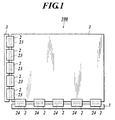
- FIG. 1 is a plan view showing an overall structure of a liquid crystal display apparatus of the embodiment of the present invention.
- FIG. 2A is a plan view showing details of an electrode portion of a liquid crystal panel and a COF electrode portion of a COF substrate.
- FIG. 2B is an enlarged view of a frame portion A of FIG. 2A .
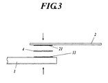
- FIG. 3 is a view for explaining an adhesion method applied to the COF substrate and the liquid crystal panel.
- FIG. 4A is a plan view showing the state in which the electrode portion of the liquid crystal panel and the COF electrode portion of the COF substrate are superposed, and
- FIG. 4B is an enlarged view of a framed portion B of FIG. 4A . Note that the scope of the present invention is not limited to the illustrated embodiment.
- a liquid crystal display apparatus 100 of the embodiment is composed of a liquid crystal panel 1 in which liquid crystal cells and transparent electrodes are formed on a glass substrate; COF substrates 2 on each of which a gate driver 23 or source driver 24 to drive the liquid crystal panel 1 is formed; and printed circuit boards (PCB) 3 on which circuits and wiring are formed for supplying electrical source voltages and various types of signals to the gate drivers 23 and the source drivers 24.
- PCB printed circuit boards
- the COF substrates 2 and the liquid crystal panel 1, and the COF substrates 2 and the printed circuit boards 3 are mechanically and electrically connected by adhering the electrodes thereof to each other with an anisotropic conductive film (ACF) 4 interposed therebetween.
- ACF anisotropic conductive film
- a plurality of electrode portions 10 where a plurality of vertically elongated fine electrodes 11 are formed, and the electrodes 11 are arrayed in a row at equal intervals a.
- a COF electrode portion 20 where a number of vertically elongated fine COF electrodes 21 are formed, and the COF electrodes 21 are arrayed in a row at equal intervals c.
- the electrodes 11 of the liquid crystal panel 1 and the COF electrodes 21 of the COF substrate 2 are disposed so as to be superposed on each other in a 1-to-1 arrangement when the COF substrate 2 and the liquid crystal panel 1 are connected to each other. Specifically, as shown in FIG. 3 , when connecting the liquid crystal panel 1 to the COF substrate 2, they are compression-bonded by aligning the electrodes 11 of the liquid crystal panel 1 and the COF electrodes 21 so as to face each other in a 1-to-1 arrangement, and then pushing the electrodes together while an anisotropic conductive film 4 is inserted therebetween.
- a length of the electrodes 11 of the liquid crystal panel 1 in a width direction (hereinafter the length in a width direction is referred to as the "electrode width") and the electrode width of the COF electrodes 21 are different, and in the embodiment, the electrode width d of the COF electrodes 21 is formed so as to be narrower than the electrode width b of the electrodes 11.
- two COF electrodes 21b disposed at both ends have the electrode widths d' which is wider than the electrode widths d of the COF electrodes (the other COF electrodes) 21a disposed on the center side of the COF electrode portion 20 by an amount equivalent to d' - d ((b - d)/2).
- the two COF electrodes 21 positioned at both ends of the COF electrode portion 20 are positioning electrodes to be collimating marks for positioning when superposition of the electrodes 11 of the liquid crystal panel 1 and the COF electrodes 21.
- these positioning electrodes 21b are dummy electrodes, and their use is limited to positioning.
- the widths d' of the positioning electrodes 21b, the widths d of the other COF electrodes 21, and the intervals c between the COF electrodes 21 (21a, 21b) described above respectively are set, according to the electrode widths b of the electrodes 11 of the liquid crystal panel 1 and the intervals a between the electrodes 11, so that when one end portion 211 in a width direction of the positioning electrodes 21b and one end portion 111 in a width direction of the one electrode 11 in the electrode portion 10 are aligned, the center in a width direction of the electrodes 11 of the liquid crystal panel 1 and the center in a width direction of the COF electrodes 21a (COF electrodes (other COF electrodes) other than positioning electrodes 21b disposed at both ends of the COF electrode portions 20) disposed on the center side of the COF electrode portions 20 are substantially align.
- any one end portion (for example, the one end portion 211 in the outward direction) in a width direction of the positioning electrodes 21b disposed at both ends of the COF electrode portion 20 is allowed to correspond to one end portion (for example, the one end portion 111 in the outward direction) in a width direction of the corresponding electrodes 11 in the electrode portion 10.
- the centers in a width direction of the COF electrodes 21a disposed on the center side of the COF electrode portion 20 are substantially superposed on the centers in a width direction of the electrodes 11 of the liquid crystal panel 1.
- the one end portion 211 outside in a width direction of the COF electrodes 21 disposed on both sides of the COF electrode portion 20 is disposed so as to be aligned with the one end portion 111 outside in a width direction of the electrodes 11 of the liquid crystal panel 1, then the electrodes 11 of the liquid crystal panel 1 and the COF electrodes 21 (21a and 21b) are correctly superposed in a 1-to-1 arrangement.
- the electrodes 11 of the liquid crystal panel 1 and the COF electrodes 21 are superposed, by confirming whether or not the one end portion (for example, the one end portion 211 in the outside direction) in a width direction of the other positioning electrode 21b and one end portion (for example, the one end portion 111 in the outside direction), in a width direction of the corresponding electrode 11 in the electrode portion 10 are aligned, it is possible to confirm reliably that superposition of the electrodes 11 of the liquid crystal panel 1 and the COF electrodes 21 has been correctly carried out.
- the apparatus 100 is equipped with the liquid crystal panel 1 including the electrode portion 10 where a plurality of the electrodes are arranged in a row; and the COF substrate 2 including the COF electrode portion 20 where a plurality of the COF electrodes 21 (21a and 21b) are arrayed in a row and have widths different from widths of the electrodes 11, and wherein the COF electrodes 21b in the COF electrode portion 20 are used as positioning electrodes when carrying out superposition of the electrodes 11 and the COF electrodes 21, and have a shape that is different from that of the other COF electrodes 21a.
- the widths of the positioning electrodes 21b and the intervals between the COF electrodes 21 are set such that the center in a width direction of the other COF electrodes 21 and the center in a width direction of the electrodes 11 are substantially superposed when the one end portion 211 in a width direction of a positioning electrode 21b and the one end portion 111 in a width direction of one electrode 11 in the electrode portion 10 are aligned.
- the positioning electrode is a COF electrode 21b at one end of the COF electrode portion 20
- the positioning electrode is disposed at the end, superposition of the electrodes 11 of the liquid crystal panel 1 and the COF electrodes 21 becomes even easier.
- the positioning electrodes are the COF electrodes 21b at both ends in the COF electrode portion 20
- the positioning electrodes 21b are dummy electrodes, even when the dimensions and properties of the positioning electrodes change due to the superposing step of the electrodes 11 of the liquid crystal panel 1 and the COF electrodes 21, this does not adversely influence the liquid crystal display apparatus.
- the electrode width of the COF electrodes 21 is narrower than the electrode width of the electrodes 11 of the liquid crystal panel 1.
- the electrode width of the COF electrodes 21 may be formed so as to be wider than the electrode width of the electrodes 11 of the liquid crystal panel 1.
- the electrode width d' of the positioning electrodes 21b is formed so as to be narrower than the electrode width b of the electrodes 11 of the liquid crystal panel 1.
- the electrode width of the positioning electrodes 21b and the electrode width of the electrodes 11 of the liquid crystal panel 1 can be made identical widths, and in the superposing step of the electrodes 11 of the liquid crystal panel 1 and the COF electrodes 21, positioning may be carried out by aligning both end portions in a width direction of the positioning electrodes and both end portions in a width direction of one electrode 11 in the liquid crystal panel 1. In this case, only the intervals between the positioning electrodes 21b and the adjacent COF electrode 21 are set so as to be smaller than the intervals between the other COF electrodes 21.
- the positioning electrodes 21b are dummy electrodes in the embodiment described above, the positioning electrodes 21b do not need to be dummy electrodes. In this case, the present invention can be formed without providing a new structure for the positioning.
- an arrangement may be provided in which two COF electrodes are connected and a slit is interposed therebetween, which slit has a width identical to the width between the electrodes 11 of the liquid crystal panel 1. Then, during the superposing step for the electrodes 11 of the liquid crystal 1 and the COF electrodes, when positioning is carried out such that the slit of the positioning electrode is disposed between the electrodes 11 of the liquid crystal panel 1, the center in a width direction of the other COF electrodes and the center in a width direction of the electrodes 11 are substantially superposed, and superposition can thereby be accurately carried out.
- a liquid crystal display apparatus including: a liquid crystal panel including an electrode portion where a plurality of electrodes are arranged in a row; and a COF substrate including a COF electrode portion where a plurality of COF electrodes are arranged in a row, which COF electrodes have widths different from widths of the electrodes, wherein at least one of the COF electrodes in the COF electrode portion is a positioning electrode for carrying out superposition of the electrodes and the COF electrodes, which positioning electrode has a shape different from shapes of other COF electrodes, and a width of the positioning electrode and an interval between the COF electrodes are set so that, when at least one end portion in a width direction of the positioning electrode and at least one end portion in a width direction of one electrode in the electrode portion are aligned, a center in a width direction of each of the other COF electrodes and a center in a width direction of each of the electrodes are substantially align.
- the positioning electrode is the COF electrode at one end of the COF electrode portion.
- the positioning electrodes are the COF electrodes at both ends of the COF electrode portion.
- the positioning electrode is a dummy electrode.
- a liquid crystal display apparatus including: a liquid crystal panel including an electrode portion where a plurality of electrodes are arranged in a row; and a COF substrate including a COF electrode portion where a plurality of COF electrodes are arranged in a row, which COF electrodes have widths different from widths of the electrodes, wherein the COF electrodes at both sides of the COF electrode portion are positioning electrodes for carrying out superposition of the electrodes and the COF electrodes, which positioning electrodes have shapes different from shapes of other COF electrodes, widths of the positioning electrodes and an interval between the COF electrodes are set so that, when at least one end portion in a width direction of the positioning electrodes and at least one end portion in a width direction of the one electrode in the electrode portion are aligned, a center in a width direction of each of the other COF electrodes and a center in a width direction of each of the electrodes are substantially align, and the positioning electrodes are
- a method for manufacturing the above liquid crystal display apparatus including a step of: carrying out positioning by allowing one end portion in a width direction of the positioning electrode positioned at one end of the COF electrode portion and one end portion in a width direction of one electrode in the electrode portion, which one electrode corresponds to the positioning electrode, to be align.
- the liquid crystal display apparatus is equipped with the liquid crystal panel including the electrode portion where a plurality of the electrodes are arranged in a row; and the COF substrate including the COF electrode portion where a plurality of the COF electrodes are arrayed in a row and have widths different from widths of the electrodes, and wherein at least one of the COF electrodes in the COF electrode portion is used as the positioning electrode when carrying out superposition of the electrodes and the COF electrodes, and have a shape different from that of the other COF electrodes.
- the width of the positioning electrode and the interval between the COF electrodes are set such that the center in a width direction of the other electrodes and the center in a width direction of the electrodes are substantially superposed when at least the one end portion in a width direction of a positioning electrode and at least the one end portion in a width direction of one electrode in the electrode portion are aligned.
Landscapes
- Physics & Mathematics (AREA)
- Nonlinear Science (AREA)
- Engineering & Computer Science (AREA)
- Mathematical Physics (AREA)
- Chemical & Material Sciences (AREA)
- Crystallography & Structural Chemistry (AREA)
- General Physics & Mathematics (AREA)
- Optics & Photonics (AREA)
- Manufacturing & Machinery (AREA)
- Microelectronics & Electronic Packaging (AREA)
- Liquid Crystal (AREA)
- Devices For Indicating Variable Information By Combining Individual Elements (AREA)
Applications Claiming Priority (1)
| Application Number | Priority Date | Filing Date | Title |
|---|---|---|---|
| JP2008122877A JP2009271383A (ja) | 2008-05-09 | 2008-05-09 | 液晶表示装置及び液晶表示装置の製造方法 |
Publications (1)
| Publication Number | Publication Date |
|---|---|
| EP2128685A1 true EP2128685A1 (de) | 2009-12-02 |
Family
ID=40799246
Family Applications (1)
| Application Number | Title | Priority Date | Filing Date |
|---|---|---|---|
| EP09159481A Withdrawn EP2128685A1 (de) | 2008-05-09 | 2009-05-06 | Flüssigkristallanzeigevorrichtung und Verfahren zur Herstellung der Flüssigkristallanzeigevorrichtung |
Country Status (3)
| Country | Link |
|---|---|
| US (1) | US20090279037A1 (de) |
| EP (1) | EP2128685A1 (de) |
| JP (1) | JP2009271383A (de) |
Families Citing this family (4)
| Publication number | Priority date | Publication date | Assignee | Title |
|---|---|---|---|---|
| KR20120063202A (ko) * | 2010-12-07 | 2012-06-15 | 삼성전자주식회사 | 반도체 패키지 및 이를 포함하는 디스플레이 패널 어셈블리 |
| CN106896592B (zh) * | 2017-02-14 | 2020-05-22 | 深圳市华星光电技术有限公司 | 液晶显示面板及显示装置 |
| US10522524B2 (en) * | 2017-06-30 | 2019-12-31 | Lg Display Co., Ltd. | Display device and method for fabricating the same |
| CN117631382A (zh) * | 2023-12-05 | 2024-03-01 | Tcl华星光电技术有限公司 | 显示装置 |
Citations (8)
| Publication number | Priority date | Publication date | Assignee | Title |
|---|---|---|---|---|
| JPH0521515A (ja) * | 1991-07-15 | 1993-01-29 | Seiko Epson Corp | 液晶表示デバイスとその製造方法 |
| EP0715201A2 (de) * | 1994-11-28 | 1996-06-05 | Canon Kabushiki Kaisha | Schaltungsanordnung und Verfahren zu deren Herstellung |
| US5982468A (en) * | 1996-03-21 | 1999-11-09 | Nec Corporation | Liquid crystal display apparatus having dummy lead and dummy land for alignment |
| JP2000111939A (ja) | 1998-08-03 | 2000-04-21 | Rohm Co Ltd | 液晶表示素子 |
| JP2000312070A (ja) | 1999-04-27 | 2000-11-07 | Optrex Corp | 電極端子の接続方法 |
| US20010020996A1 (en) * | 2000-03-09 | 2001-09-13 | Advanced Display Inc. | Liquid crystal display |
| JP2002026593A (ja) * | 2000-06-30 | 2002-01-25 | Shibaura Mechatronics Corp | 部品実装装置及び部品実装方法 |
| US6583845B1 (en) * | 2000-02-23 | 2003-06-24 | Lg.Philips Lcd Co., Ltd. | Liquid crystal display device and method of fabricating the same |
Family Cites Families (7)
| Publication number | Priority date | Publication date | Assignee | Title |
|---|---|---|---|---|
| JPH07283503A (ja) * | 1994-04-08 | 1995-10-27 | Seiko Instr Inc | 回路基板 |
| JPH0990398A (ja) * | 1995-09-26 | 1997-04-04 | Casio Comput Co Ltd | 電気配線基板の接続構造 |
| JPH10209581A (ja) * | 1997-01-24 | 1998-08-07 | Seiko Epson Corp | プリント配線板、液晶表示装置及び電子機器 |
| JP3734194B2 (ja) * | 1997-04-25 | 2006-01-11 | オプトレックス株式会社 | 液晶表示装置 |
| JP2001228806A (ja) * | 2000-02-21 | 2001-08-24 | Toshiba Corp | 平面表示装置 |
| JP4271435B2 (ja) * | 2002-12-09 | 2009-06-03 | シャープ株式会社 | 半導体装置 |
| JP2007234915A (ja) * | 2006-03-02 | 2007-09-13 | Sony Corp | 配線基板、配線ケーブル、電子機器および配線接続方法 |
-
2008
- 2008-05-09 JP JP2008122877A patent/JP2009271383A/ja active Pending
-
2009
- 2009-05-06 EP EP09159481A patent/EP2128685A1/de not_active Withdrawn
- 2009-05-06 US US12/436,509 patent/US20090279037A1/en not_active Abandoned
Patent Citations (9)
| Publication number | Priority date | Publication date | Assignee | Title |
|---|---|---|---|---|
| JPH0521515A (ja) * | 1991-07-15 | 1993-01-29 | Seiko Epson Corp | 液晶表示デバイスとその製造方法 |
| EP0715201A2 (de) * | 1994-11-28 | 1996-06-05 | Canon Kabushiki Kaisha | Schaltungsanordnung und Verfahren zu deren Herstellung |
| US5982468A (en) * | 1996-03-21 | 1999-11-09 | Nec Corporation | Liquid crystal display apparatus having dummy lead and dummy land for alignment |
| JP2000111939A (ja) | 1998-08-03 | 2000-04-21 | Rohm Co Ltd | 液晶表示素子 |
| JP2000312070A (ja) | 1999-04-27 | 2000-11-07 | Optrex Corp | 電極端子の接続方法 |
| US6583845B1 (en) * | 2000-02-23 | 2003-06-24 | Lg.Philips Lcd Co., Ltd. | Liquid crystal display device and method of fabricating the same |
| US20010020996A1 (en) * | 2000-03-09 | 2001-09-13 | Advanced Display Inc. | Liquid crystal display |
| JP2001255550A (ja) | 2000-03-09 | 2001-09-21 | Advanced Display Inc | 液晶表示素子 |
| JP2002026593A (ja) * | 2000-06-30 | 2002-01-25 | Shibaura Mechatronics Corp | 部品実装装置及び部品実装方法 |
Also Published As
| Publication number | Publication date |
|---|---|
| JP2009271383A (ja) | 2009-11-19 |
| US20090279037A1 (en) | 2009-11-12 |
Similar Documents
| Publication | Publication Date | Title |
|---|---|---|
| CN112435619B (zh) | 显示模组及显示模组的测试方法 | |
| KR101195688B1 (ko) | 플렉시블 기판 및 전기 회로 구조체 | |
| US20120262886A1 (en) | Display Device | |
| US7349054B2 (en) | Method of mounting flexible circuit boards, and display device | |
| KR100464066B1 (ko) | 플렉시블 인쇄회로 및 배선기판을 상호접속하기 위한 구조및 방법과, 액정표시장치, 및 그 제조방법 | |
| JP4059750B2 (ja) | 電子モジュールおよびその製造方法 | |
| US20100182293A1 (en) | Display module, liquid crystal display device and method for manufacturing display module | |
| US6300998B1 (en) | Probe for inspecting liquid crystal display panel, and apparatus and method for inspecting liquid crystal display panel | |
| US7656089B2 (en) | Tape carrier package on reel and plasma display device using the same | |
| US7420821B2 (en) | Electronic module and driving circuit board therefor | |
| US20040159930A1 (en) | Semiconductor device, method of manufacturing the same, and electronic device using the semiconductor device | |
| KR100574278B1 (ko) | 테이프 캐리어 패키지 및 이를 이용한 액정표시기모듈 | |
| US20090279037A1 (en) | Liquid Crystal Display Apparatus and Method for Manufacturing Liquid Crystal Display Apparatus | |
| KR20010088389A (ko) | 액정표시소자 | |
| US8203684B2 (en) | Liquid crystal module | |
| JP3645172B2 (ja) | 半導体集積回路装置搭載用基板 | |
| US8615871B2 (en) | Chip mounted wiring substrate | |
| JP2001056477A (ja) | 液晶表示装置及びその検査方法 | |
| JP2016207792A (ja) | フレキシブルプリント基板、および画像表示装置 | |
| JP2008130803A (ja) | 基板装置および基板 | |
| JP2006276115A (ja) | 液晶モジュール | |
| US8975756B2 (en) | Electric terminal device and method of connecting the same | |
| KR101020625B1 (ko) | 필름타입 프로브유닛 및 그의 제조방법 | |
| JPH07183634A (ja) | パネルの実装構造および実装方法並びにフレキシブル配線板並びに駆動ic交換方法 | |
| JP2001183692A (ja) | 液晶装置及びその位置合わせ方法 |
Legal Events
| Date | Code | Title | Description |
|---|---|---|---|
| PUAI | Public reference made under article 153(3) epc to a published international application that has entered the european phase |
Free format text: ORIGINAL CODE: 0009012 |
|
| AK | Designated contracting states |
Kind code of ref document: A1 Designated state(s): AT BE BG CH CY CZ DE DK EE ES FI FR GB GR HR HU IE IS IT LI LT LU LV MC MK MT NL NO PL PT RO SE SI SK TR |
|
| 17P | Request for examination filed |
Effective date: 20091007 |
|
| 17Q | First examination report despatched |
Effective date: 20140408 |
|
| STAA | Information on the status of an ep patent application or granted ep patent |
Free format text: STATUS: THE APPLICATION IS DEEMED TO BE WITHDRAWN |
|
| 18D | Application deemed to be withdrawn |
Effective date: 20140819 |