EP0715201A2 - Schaltungsanordnung und Verfahren zu deren Herstellung - Google Patents
Schaltungsanordnung und Verfahren zu deren Herstellung Download PDFInfo
- Publication number
- EP0715201A2 EP0715201A2 EP95308488A EP95308488A EP0715201A2 EP 0715201 A2 EP0715201 A2 EP 0715201A2 EP 95308488 A EP95308488 A EP 95308488A EP 95308488 A EP95308488 A EP 95308488A EP 0715201 A2 EP0715201 A2 EP 0715201A2
- Authority
- EP
- European Patent Office
- Prior art keywords
- substrate
- electrodes
- circuit assembly
- electrode
- assembly according
- Prior art date
- Legal status (The legal status is an assumption and is not a legal conclusion. Google has not performed a legal analysis and makes no representation as to the accuracy of the status listed.)
- Withdrawn
Links
Images


Classifications
-
- G—PHYSICS
- G02—OPTICS
- G02F—OPTICAL DEVICES OR ARRANGEMENTS FOR THE CONTROL OF LIGHT BY MODIFICATION OF THE OPTICAL PROPERTIES OF THE MEDIA OF THE ELEMENTS INVOLVED THEREIN; NON-LINEAR OPTICS; FREQUENCY-CHANGING OF LIGHT; OPTICAL LOGIC ELEMENTS; OPTICAL ANALOGUE/DIGITAL CONVERTERS
- G02F1/00—Devices or arrangements for the control of the intensity, colour, phase, polarisation or direction of light arriving from an independent light source, e.g. switching, gating or modulating; Non-linear optics
- G02F1/01—Devices or arrangements for the control of the intensity, colour, phase, polarisation or direction of light arriving from an independent light source, e.g. switching, gating or modulating; Non-linear optics for the control of the intensity, phase, polarisation or colour
- G02F1/13—Devices or arrangements for the control of the intensity, colour, phase, polarisation or direction of light arriving from an independent light source, e.g. switching, gating or modulating; Non-linear optics for the control of the intensity, phase, polarisation or colour based on liquid crystals, e.g. single liquid crystal display cells
- G02F1/133—Constructional arrangements; Operation of liquid crystal cells; Circuit arrangements
- G02F1/1333—Constructional arrangements; Manufacturing methods
- G02F1/1345—Conductors connecting electrodes to cell terminals
-
- H—ELECTRICITY
- H05—ELECTRIC TECHNIQUES NOT OTHERWISE PROVIDED FOR
- H05K—PRINTED CIRCUITS; CASINGS OR CONSTRUCTIONAL DETAILS OF ELECTRIC APPARATUS; MANUFACTURE OF ASSEMBLAGES OF ELECTRICAL COMPONENTS
- H05K3/00—Apparatus or processes for manufacturing printed circuits
- H05K3/36—Assembling printed circuits with other printed circuits
- H05K3/361—Assembling flexible printed circuits with other printed circuits
-
- G—PHYSICS
- G02—OPTICS
- G02F—OPTICAL DEVICES OR ARRANGEMENTS FOR THE CONTROL OF LIGHT BY MODIFICATION OF THE OPTICAL PROPERTIES OF THE MEDIA OF THE ELEMENTS INVOLVED THEREIN; NON-LINEAR OPTICS; FREQUENCY-CHANGING OF LIGHT; OPTICAL LOGIC ELEMENTS; OPTICAL ANALOGUE/DIGITAL CONVERTERS
- G02F1/00—Devices or arrangements for the control of the intensity, colour, phase, polarisation or direction of light arriving from an independent light source, e.g. switching, gating or modulating; Non-linear optics
- G02F1/01—Devices or arrangements for the control of the intensity, colour, phase, polarisation or direction of light arriving from an independent light source, e.g. switching, gating or modulating; Non-linear optics for the control of the intensity, phase, polarisation or colour
- G02F1/13—Devices or arrangements for the control of the intensity, colour, phase, polarisation or direction of light arriving from an independent light source, e.g. switching, gating or modulating; Non-linear optics for the control of the intensity, phase, polarisation or colour based on liquid crystals, e.g. single liquid crystal display cells
- G02F1/133—Constructional arrangements; Operation of liquid crystal cells; Circuit arrangements
- G02F1/1333—Constructional arrangements; Manufacturing methods
- G02F1/133354—Arrangements for aligning or assembling substrates
-
- G—PHYSICS
- G02—OPTICS
- G02F—OPTICAL DEVICES OR ARRANGEMENTS FOR THE CONTROL OF LIGHT BY MODIFICATION OF THE OPTICAL PROPERTIES OF THE MEDIA OF THE ELEMENTS INVOLVED THEREIN; NON-LINEAR OPTICS; FREQUENCY-CHANGING OF LIGHT; OPTICAL LOGIC ELEMENTS; OPTICAL ANALOGUE/DIGITAL CONVERTERS
- G02F2202/00—Materials and properties
- G02F2202/28—Adhesive materials or arrangements
-
- H—ELECTRICITY
- H05—ELECTRIC TECHNIQUES NOT OTHERWISE PROVIDED FOR
- H05K—PRINTED CIRCUITS; CASINGS OR CONSTRUCTIONAL DETAILS OF ELECTRIC APPARATUS; MANUFACTURE OF ASSEMBLAGES OF ELECTRICAL COMPONENTS
- H05K1/00—Printed circuits
- H05K1/02—Details
- H05K1/0266—Marks, test patterns or identification means
- H05K1/0269—Marks, test patterns or identification means for visual or optical inspection
-
- H—ELECTRICITY
- H05—ELECTRIC TECHNIQUES NOT OTHERWISE PROVIDED FOR
- H05K—PRINTED CIRCUITS; CASINGS OR CONSTRUCTIONAL DETAILS OF ELECTRIC APPARATUS; MANUFACTURE OF ASSEMBLAGES OF ELECTRICAL COMPONENTS
- H05K1/00—Printed circuits
- H05K1/02—Details
- H05K1/11—Printed elements for providing electric connections to or between printed circuits
- H05K1/117—Pads along the edge of rigid circuit boards, e.g. for pluggable connectors
-
- H—ELECTRICITY
- H05—ELECTRIC TECHNIQUES NOT OTHERWISE PROVIDED FOR
- H05K—PRINTED CIRCUITS; CASINGS OR CONSTRUCTIONAL DETAILS OF ELECTRIC APPARATUS; MANUFACTURE OF ASSEMBLAGES OF ELECTRICAL COMPONENTS
- H05K2201/00—Indexing scheme relating to printed circuits covered by H05K1/00
- H05K2201/01—Dielectrics
- H05K2201/0104—Properties and characteristics in general
- H05K2201/0108—Transparent
-
- H—ELECTRICITY
- H05—ELECTRIC TECHNIQUES NOT OTHERWISE PROVIDED FOR
- H05K—PRINTED CIRCUITS; CASINGS OR CONSTRUCTIONAL DETAILS OF ELECTRIC APPARATUS; MANUFACTURE OF ASSEMBLAGES OF ELECTRICAL COMPONENTS
- H05K2201/00—Indexing scheme relating to printed circuits covered by H05K1/00
- H05K2201/03—Conductive materials
- H05K2201/032—Materials
- H05K2201/0326—Inorganic, non-metallic conductor, e.g. indium-tin oxide [ITO]
-
- H—ELECTRICITY
- H05—ELECTRIC TECHNIQUES NOT OTHERWISE PROVIDED FOR
- H05K—PRINTED CIRCUITS; CASINGS OR CONSTRUCTIONAL DETAILS OF ELECTRIC APPARATUS; MANUFACTURE OF ASSEMBLAGES OF ELECTRICAL COMPONENTS
- H05K2201/00—Indexing scheme relating to printed circuits covered by H05K1/00
- H05K2201/09—Shape and layout
- H05K2201/09209—Shape and layout details of conductors
- H05K2201/09654—Shape and layout details of conductors covering at least two types of conductors provided for in H05K2201/09218 - H05K2201/095
- H05K2201/09781—Dummy conductors, i.e. not used for normal transport of current; Dummy electrodes of components
-
- H—ELECTRICITY
- H05—ELECTRIC TECHNIQUES NOT OTHERWISE PROVIDED FOR
- H05K—PRINTED CIRCUITS; CASINGS OR CONSTRUCTIONAL DETAILS OF ELECTRIC APPARATUS; MANUFACTURE OF ASSEMBLAGES OF ELECTRICAL COMPONENTS
- H05K2201/00—Indexing scheme relating to printed circuits covered by H05K1/00
- H05K2201/09—Shape and layout
- H05K2201/09818—Shape or layout details not covered by a single group of H05K2201/09009 - H05K2201/09809
- H05K2201/09918—Optically detected marks used for aligning tool relative to the PCB, e.g. for mounting of components
-
- H—ELECTRICITY
- H05—ELECTRIC TECHNIQUES NOT OTHERWISE PROVIDED FOR
- H05K—PRINTED CIRCUITS; CASINGS OR CONSTRUCTIONAL DETAILS OF ELECTRIC APPARATUS; MANUFACTURE OF ASSEMBLAGES OF ELECTRICAL COMPONENTS
- H05K2203/00—Indexing scheme relating to apparatus or processes for manufacturing printed circuits covered by H05K3/00
- H05K2203/16—Inspection; Monitoring; Aligning
- H05K2203/166—Alignment or registration; Control of registration
-
- H—ELECTRICITY
- H05—ELECTRIC TECHNIQUES NOT OTHERWISE PROVIDED FOR
- H05K—PRINTED CIRCUITS; CASINGS OR CONSTRUCTIONAL DETAILS OF ELECTRIC APPARATUS; MANUFACTURE OF ASSEMBLAGES OF ELECTRICAL COMPONENTS
- H05K3/00—Apparatus or processes for manufacturing printed circuits
- H05K3/30—Assembling printed circuits with electric components, e.g. with resistors
- H05K3/32—Assembling printed circuits with electric components, e.g. with resistors electrically connecting electric components or wires to printed circuits
- H05K3/321—Assembling printed circuits with electric components, e.g. with resistors electrically connecting electric components or wires to printed circuits by conductive adhesives
- H05K3/323—Assembling printed circuits with electric components, e.g. with resistors electrically connecting electric components or wires to printed circuits by conductive adhesives by applying an anisotropic conductive adhesive layer over an array of pads
Definitions
- the present invention relates to a circuit assembly for use in display apparatus, image sensors, recording heads, light-emitting device arrays, etc., and a process for production thereof.
- a circuit assembly is frequency used in many electrical apparatus or devices of almost all aspects, typical application examples of which may include display devices inclusive of a liquid crystal device, a plasma device, DMD, and a electrochromic device; image sensors, inclusive of a thin-film type sensor comprising amorphous silicon, and a multi-tip-type sensor provided with an arranged plurality of IC chips; recording heads, inclusive of a thermal head and an ink jet head; and light-emitting device arrays, inclusive of an LED array, and an electron discharge device array.
- display devices inclusive of a liquid crystal device, a plasma device, DMD, and a electrochromic device
- image sensors inclusive of a thin-film type sensor comprising amorphous silicon, and a multi-tip-type sensor provided with an arranged plurality of IC chips
- recording heads inclusive of a thermal head and an ink jet head
- light-emitting device arrays inclusive of an LED array, and an electron discharge device array.
- Figure 1 shows a liquid crystal display apparatus (as an example of circuit assembly) including a combination of a liquid crystal panel (first circuit substrate) P and TAB films for liquid crystal drive (second circuit substrates) 7 connected to the liquid crystal panel P.
- the liquid crystal display apparatus 1 includes a liquid crystal panel P, which comprises a glass substrate 2 on which data electrodes are disposed, and a glass substrate 3 on which scanning electrodes are disposed.
- the glass substrates 2 and 3 do not have the same shape, but the glass substrate 2 protrudes out of the other glass substrate 3 at both upper and lower edges, and the glass substrate 3 protrudes out of the glass substrate 2 at the left edge.
- One glass substrate 2 is provided with a large number of stripe-shaped data electrodes 5 disposed on one surface thereof, and the other glass substrate 3 is provided with a large number of similarly stripe-shaped scanning electrodes 6.
- Electrodes 5 and 6 are extended up to the edges of the substrates 2 and 3, so that the data electrodes 5 are exposed outside at the upper and lower peripheries of the glass substrate 2, and the scanning electrodes 6 are exposed outside at the left periphery of the glass substrate 3.
- the glass substrates 2 and 3 are disposed opposite to each other so as to sandwich a liquid crystal therebetween with their electrode-provided surfaces.
- FIGS. 2A - 2C are a top plan view, a bottom plan view and a thicknesswise sectional view, respectively, of such a TAB film 7.
- the liquid crystal-drive TAB film 7 comprises a soft base film 7a of, e.g., polyimide resin, etc., on which input terminals 7b and output terminals 7c are formed of, e.g., patterned copper foil electrodes, and a liquid crystal-device IC chip (drive semiconductor) 7d is mounted by TAB between and connected with the terminals 7b and 7c.
- Signals inputted to the input terminals 7b of the TAB film 7 are converted into signals of prescribed waveforms by a liquid crystal-drive IC chip 7d and then to the electrodes 5 and 6 of the liquid crystal panel P to drive the liquid crystal panel P for displaying various data.
- the base film 7a may be formed by stamping a film carrier tape as a flexible circuit substrate.
- the input terminals 7b and 7c may be formed by etching of a copper foil or film formed on the base film 7a into a prescribed pattern and further plating with Au or Sn. As shown in Figure 7C, a portion of the base film 7a may be removed to provide the input terminal 7b with a partially overhanging structure or separation from the base film 7a and generally further coverage with an elastomer or resin so that an external stress applied to the base film is prevented from being directly applied to the input terminal 7b. A similar overhang structure or separation from the base film 7b may also be given to the output terminal 7c.
- the above-mentioned liquid crystal-drive TAB film 7 and the liquid crystal panel P may be connected to each other in the following manner.
- the TAB film 7 and the panel P are respectively provided with an alignment mark for positional alignment therebetween.
- Figure 3 is a schematic side illustration for illustrating a manner of the positional alignment.
- an anisotropic electroconductive adhesive (member) 9 is used for the connection.
- the alignment apparatus includes a liquid crystal panel alignment unit 100 for carrying the liquid crystal panel P, and the unit 100 is arranged so as to be movable freely in three-dimensional directions.
- the apparatus further includes a TAB alignment unit 101 for carrying the liquid crystal drive TAB film 7, and the unit is also arranged so as to be freely movable three-dimensionally.
- the apparatus also includes a camera 10 for monitoring the positions of the liquid crystal panel P and the TAB film 7, so that the alignment mark on the liquid crystal panel P (hereinafter called “substrate-side mark” or "panel-side mark”) is observed under vertical falling illumination and the alignment mark on the TAB film 7 (hereinafter called "TAB-side mark”) is observed under illumination with side illumination light.
- the vertical falling illumination is a manner of illuminating an object through an objective lens while disposing a semitransparent mirror between the objective lens and an image forming position
- the illumination with side-illumination light is dark-field illumination of illuminating an object with illumination light obliquely incident to the object, both being well known in the field of an optical microscope (see, e.g., "Kogaku Gijutsu Handbook” (Optical Technology Handbook), page 852 (published from Asakura Shoten K.K.).
- the camera 10 is disposed on a backside of the liquid crystal panel P (opposite side of the liquid crystal-drive TAB film 7), so that the substrate-side mark is observed through the glass substrate 3 and the TAB-side mark is observed through the glass substrate 3 and transparent films (transparent conductor films and the anisotropic conductive adhesive, etc.) formed on the substrate.
- the liquid crystal panel P is loaded on the liquid crystal panel alignment unit 100, and the liquid crystal-drive TAB film 7 is loaded on the TAB alignment unit 101. Then, the TAB-side mark and the substrate-side mark are recognized by the camera 10 to calculate an amount of positional deviation between both marks. Based on the amount of the positional deviation, both or either one of the alignment units may be moved to effect a positional adjustment between the liquid crystal panel P and the TAB film 7, whereby the electrodes 5 and 6 of the liquid crystal panel P are positionally aligned with the output terminals 7c on the TAB film 7.
- the above-mentioned data electrodes 5 and the scanning electrodes 6 may be composed of transparent electrodes of ITO, etc., or metal electrodes.
- the substrate-side mark may also be formed of the same transparent electrode material.
- the contrast between substrate-side mark and the glass substrates 2 and 3 becomes small while it depends on the thickness of the transparent electrodes, so that the image recognition by the camera 10 is found to be very difficult.
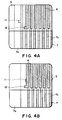
- FIGs 4A and 4B are schematic views showing images observed in the finder of the camera 10. In case where a TAB-side mark 11 is not aligned with an electrode 6 as shown in Figure 4A, the mark can be recognized. However, in case where the mark 11 is hidden by an electrode 6 as shown in Figure 4B, the image processing with the camera is hindered so that the positional alignment becomes impossible.
- a principal object of the present invention is to provide a circuit assembly having solved the above-mentioned problems and allowing an accurate positional alignment.
- Another object of the present invention is to provide a circuit assembly allowing an accurate positional alignment even in case of using an alignment mark of a simple structure.
- a further object of the present invention is to provide a process for producing such a circuit assembly.
- a circuit assembly comprising: a transparent first substrate having thereon a plurality of first electrodes, and a second substrate having thereon a plurality of second electrodes and at least partially superposed with the first substrate so that the mutually corresponding first and second electrodes are superposed and electrically connected with each other, wherein the first electrode has a light-transmissive layer and an opaque layer laminated with the light transmissive layer, and a portion of the first electrode superposed with the second substrate at least partially includes a light-transmissive portion, and the first or second substrate has an alignment mark at a position thereof corresponding to the light-transmissive portion of the first electrode.
- a process for producing a circuit assembly comprising the steps of: providing a light-transmissive first substrate having thereon a group of first electrodes including a first electrode having a light-transmissive portion and first electrodes having an opaque portion, providing a second substrate having thereon a group of second electrodes and an alignment mark, superposing the first and second substrates with an adhesive disposed therebetween, positionally aligning the first and second substrates by means of said alignment mark; and bonding the first and second substrates to each other.
- Figure 1 is a schematic plan view of a display apparatus including a circuit assembly.
- Figures 2A - 2C are a top plan view, a reversed plan view and a side sectional view of a TAB film used in a circuit assembly.
- Figure 3 is a schematic side view of a positional alignment apparatus for a circuit assembly.
- Figures 4A an 4B are views observed through a camera for positional alignment of a circuit assembly.
- Figure 5 is a schematic partial plan view of an embodiment of the carrier assembly according to the invention.
- Figure 6 is a schematic plan view of an example of substrate used in a circuit assembly according to the invention.
- Figure 7 is a schematic sectional view of an embodiment of the circuit assembly according to the invention.
- Figure 8 is a flow chart for describing an embodiment of the process for producing a circuit assembly according to the invention.
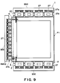
- Figure 9 is a schematic plan view of a liquid crystal display apparatus including a first embodiment of the circuit assembly according to the invention.
- Figure 10 is a schematic plan view of a first substrate used in the first embodiment of the circuit assembly.
- Figure 11 is a schematic plan view of a second substrate used in the first embodiment of the circuit assembly.
- Figure 12 is a partial schematic plan view of a circuit assembly before positional alignment.
- Figure 13 is a partial schematic plan view of a circuit assembly after positional alignment.
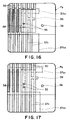
- Figure 14 is a schematic plan view from the reverse side of a first substrate used in the second embodiment of the circuit assembly.
- Figure 15 is a schematic plan view of a second substrate used in the second embodiment of the circuit assembly.
- Figure 16 is a partial schematic plan view of a circuit assembly before positional alignment.
- Figure 17 is a partial schematic plan view of a circuit assembly after positional alignment.
- Figure 5 is a schematic partial plan view of an embodiment of the circuit assembly according to the present invention.
- the circuit assembly includes a light-transmissive first substrate 203 on which first electrodes 200 are disposed.
- Each first electrode 200 has an opaque portion 201 and a transparent portion 202.
- the circuit assembly also includes a second substrate 207, on which second electrodes 217 and an alignment mark 209 are disposed.
- Figure 5 shows a transient state during a positional alignment step, so that a major portion of the mark 209 overlaps one of the first electrodes 202 but, if the first substrate 203 is moved in a direction X or the second substrate 207 is moved in a direction opposite to the direction X, such a positional relationship can be established that the corresponding first and second electrodes are respectively superposed with each other and the mark 209 is free from overlapping with any of the first electrodes. This is a suitable position for electrode connection.
- each first electrode 200 corresponding to the alignment mark 209 is light-transmissive, so that the mark 209 can be recognized through the light-transmissive portion even if the mark 209 and the first electrodes are superposed so that missing of the mark 209 during the alignment step can be avoided.
- the alignment mark 209 may be disposed in contact with the first electrode (i.e.,., one of the first electrodes) 200 as shown in Figure 5 or in separation from the first electrode. However, in the case of disposing a plurality (first or second) substrates for connection with the other type of substrate as shown in Figure 1, the mark 209 may preferably be disposed in contact with or in close proximity with the first electrode.
- the mark 209 on the first substrate 203 and the second electrodes 207 per se may be used also as an alignment mark for the second substrate 207.
- both the first and second substrates are provided with respective alignment marks exclusively used for that purpose as shown in a later-described embodiment.
- the two exclusive alignment marks are disposed so as not to overlap each other in a position aligned as suitable for electrical connection.
- All the first electrodes 200 need not be provided with a light-transmissive position but at least one first electrode preferably disposed at an extreme side may be provided with such a light-transmissive portion.
- the mark which can be disposed on the first substrate 203 may preferably be opaque and may preferably be disposed at a position discrete from the opaque portions 201 of the first electrodes 200.
- Figure 6 is a partial schematic plan view of an example of such a light-transmissive first substrate.
- FIG. 6 shows 4 arrays each composed of a number (n) of electrodes including a number (b) of light-transmissive electrodes on both sides B and a number (a) of opaque electrodes in a central region A.
- the number a is at least 1, preferably 2 or more, further preferably 4 or more, but the light-transmissive electrode in a region B need not necessarily be provided in a separate plurality if it is provided with a required area corresponding to such a plurality of electrodes.
- the electrodes in the region A are connected to functional elements, such as display pixels, photoelectric conversion elements and light-emitting elements.
- the electrodes in the region(s) B may also be connected to such functional elements but can be dummy electrodes not connected to such functional elements.
- Each region B may be provided in a width (i.e., length in a direction of disposition) PT1 which may be at most 1/10, preferably at most 1/20, further preferably at most 1/50, of a width PT2 of the region A.
- the adjacent arrays may be disposed with a spacing PT3 larger than PT1 so that one alignment mark 230 each is provided in two regions each having a width of a half of PT3 so as to allow a high-density disposition.
- Each electrode may have a width of 5 - 800 ⁇ m, preferably 20 - 250 ⁇ m and may be disposed with a spacing of 5 - 800 ⁇ m preferably 20 - 250 ⁇ m from each adjacent electrode.
- the above-mentioned electrode size, spacing and number of disposition thereof may suitably be applied to a circuit assembly as shown in Figure 1 or 6 wherein one substrate (2, 3 or 203) is connected with a plurality of other substrates (7) so as to allow easy assemblage.
- Figure 7 is a partial schematic sectional view of a circuit assembly according to an embodiment of the present invention which is in a state after positional alignment and before bonding (electrical connection).
- the structure may be understood as a sectional view taken along a dot-and-dash line Z-Z in Figure 6 when the substrate shown in Figure 6 is superposed with a substrate as shown in Figures 2A - 2C.
- the circuit assembly includes light-transmissive electrodes 212d in the region B, and functionally opaque electrodes including a non-light-transmissive conductor layer 211 and a light-transmissive conductor layer 212.
- Opaque electrodes 217 are disposed on an opposite second substrate 207, on which are further disposed opaque electrodes 217d and alignment marks 209 in a region corresponding to the region B.
- an anisotropic electroconductive adhesive 250 which comprises electroconductive fine particles 251 and an adhesive resin 252 which may be a curable-type resin, i.e., a thermosetting resin, photosetting resin or thermo-photosetting resin, or a non-curable type resin.
- an adhesive resin 252 which may be a curable-type resin, i.e., a thermosetting resin, photosetting resin or thermo-photosetting resin, or a non-curable type resin.
- the electrodes in the region B are dummy electrodes, even when a force for separating both substrate occurs due, e.g., to a thermal strain or a compression force, the force may be absorbed by the electrodes to stabilize the connection between the electrodes (211, 212) and the electrodes (217).
- the first substrate used in the present invention may be a light-transmissive substrate which is light-transmissive at least in a region required for positional alignment.
- the first substrate may comprise a substrate, generally a sheet, of a light-transmissive material such as glass, quartz, alumina or resin.
- the second substrate used in the present invention may be either light-transmissive or non-light-transmissive and either rigid or flexible.
- the rigid substrate may comprise a material similar to that of the first substrate, or ceramic or metal.
- the flexible substrate material may include polyimide, polyester and epoxy glass.
- the first electrode may preferably comprise a laminated structure including a light-transmissive layer and a non-light-transmissive layer which may be disposed in this order or in an opposite order.
- the light-transmissive layer may for example comprise tin oxide, indium oxide, or indium tin oxide (ITO).
- the non-transmissive layer may comprise a metal, such as aluminum, chromium, molybdenum, tungsten, titanium, copper, gold, silver, or platinum; or an alloy of these metals alone or with other metals optionally containing an appropriate amount of non-metallic elements, such as silicon, nitrogen and oxygen.
- light-transmissive or “transparent” used herein refers to a property of allowing a required level of transmission of light used for positional alignment
- non-light-transmissive or “opaque” refers to a property of interrupting the transmission of light used for positional alignment in a level for providing an appropriate level of contrast.
- a particularly preferred example of combination of light-transmissive and non-light-transmissive material may include a combination of a transparent metal oxide and a metal so as to provide a sufficient contrast between the light-transmissive electrodes and non-light-transmissive electrodes or alignment marks.
- Figure 8 is a flow chart representing an embodiment of the process for producing a circuit assembly according to the present invention.
- a first substrate is provided (S11), a light-transmissive conductor film is formed thereon (S12), and a non-light-transmissive conductor layer is formed thereon (S13). Then the light-transmissive and non-light-transmissive conductor films are selectively etched to provide an electrode pattern (S14, S15).
- a second substrate is provided (S21), and a non-light-transmissive conductor film is formed (S22) and patterned (S23) thereon.
- an anisotropic electroconductive adhesive is provided (S33), and the first and second substrates are superposed with each other with the adhesive on at least one thereof (S41) and subjected to a rough positional alignment therebetween by observation with eyes (S42).
- the electrodes on both substrates are press-bonded to each other while avoiding a positional deviation.
- the adhesive may be cured so as to ensure the reliability of the bonding.
- the camera used for the auto-alignment may preferably be of a type allowing the vertical falling illumination and the dark field illumination and may preferably be provided with a data process circuit for calculating a positional deviation of alignment marks and a drive unit for driving alignment units carrying the first and second substrates.
- Figure 9 is a schematic plan view of a liquid crystal display apparatus including a circuit assembly according to this embodiment.
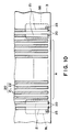
- FIG 10 is an enlarged partial view of a part (RMK2) of the liquid crystal display apparatus of Figure 9, showing an electrode pattern on a glass substrate 3 constituting the part (RMK2).
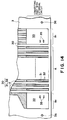
- FIG 11 is an enlarged partial view of a part (RMK2) of the apparatus of Figure 9, showing an electrode pattern on a TAB film 27.
- the liquid crystal display apparatus includes a liquid crystal panel P1, TAB films 27 carrying a drive IC chip, and bus substrates BSS, BSO and BSE.
- TAB films 27 are connected to the bus substrate BSO so that the IC chips 27d thereon are supplied with display data for odd-numbered data electrodes and drive signals for the IC chips 27d per se via the bus substrate BSO.
- the bus substrate BSE has a function of transferring display data for even-numbered data electrodes and drive signals for IC chips 27d connected thereto.
- the bus substrate BSS is connected with 11 TAB films 27 and has a function of transferring signals, such as clock pulses, address data and reference voltages so as to have the IC chips 27d on the TAB films 27 generate signals supplied to the scanning electrodes.
- the glass substrate 3 of the liquid crystal panel P1 is provided with a large number of scanning electrodes 20 each in the form of a stripe as shown in Figure 10.
- the scanning electrodes 20 in the central region A of the glass substrate 3 have a laminated structure of a transparent electrode 21 and a metal electrode 22, and a large number thereof extends up to the edge or periphery (exposed part) of the glass substrate 3.
- the scanning electrodes 20 on both outsides of the region A have such a laminated structure including a metal electrode up to their intermediate point and have a single layer structure of a transparent electrode 21 in peripheral side regions BR and BL.
- the metal electrodes 20 have a function of lowering the electric resistance of the electrodes 20 to provide an increased drive speed of the liquid crystal panel.
- the transparent electrodes 21 have the same width as the metal electrode 20 and their full width is coated by the metal electrodes 22.
- the liquid crystal panel P1 in this embodiment is designed to be driven by the electrodes 20 in the region A, and the electrodes 20 in the side regions BR and BL do not participate in the drive, thus constituting so-called dummy electrodes.
- the two side regions BR and BL are respectively provided with a panel-side mark (first alignment mark) 23.
- the panel-side marks 23 are formed outside of and in the proximity of the outermost electrodes 20 and respectively formed in an almost square pattern.
- Figure 10 shows only a structure regarding one glass-substrate 3, but actually the other glass substrate 2 are also provided with data electrodes and panel-side marks of similar shapes so as to form a circuit assembly together with TAB films connected to the data electrodes.
- the TAB film (second circuit substrate) 27 forming a circuit assembly together with the glass substrate 3 has a structure including TAB-side marks (second alignment marks) 29 as will be described with reference to Figure 11.
- the TAB film 27 has a structure almost similar to that of a conventional one and includes a base film (substrate) 27a, input terminals 27b (not shown in Figure 11), output terminals 27c and liquid crystal drive ICs 27d (not shown in Figure 11) mounted between the input and output terminals.
- the output terminals 27 each have a stripe-shape and are formed by coating a stripe of copper foil with Au or Sn plating.
- the number of the output terminals 27c and a spacing therebetween correspond to those of the electrodes 20 on the glass substrate 3.
- the outermost output terminals 27c are each provided with a TAB-side mark 20 formed in contact therewith.
- the TAB-side marks 29 are of the same material as the output terminals 27c.
- the marks 27 are left un-removed during etching for patterning of the output terminals 27c.
- the panel-side marks 23 and the TAB-side marks 29 are formed in such positions that they are not superposed with each other in an appropriately aligned and joined state of the liquid crystal panel P1 and the liquid crystal-drive TAB-film 27.
- the two TAB-side marks 29 are disposed with a spacing therebetween equal to that between the two panel-side marks 23 but the marks 29 and the marks 23 are deviated from each other in a longitudinal direction of the electrodes 20 in the normally joined position as shown in Figure 13.
- Figures 12 and 13 show a state wherein the glass substrate 3 of the panel P1 is superposed while directing its front surface downwards with an upwardly directed front surface of the TAB film 27 shown in Figure 11 as a view observed through a camera finder from the backside of the glass substrate 3 of the panel P1 so as to show a region including the region BR of the glass substrate 3 and the region CL of the TAB film 27.
- the liquid crystal panel P1 is mounted on the liquid crystal panel alignment unit and the TAB film 27 is mounted on the TAB alignment unit.
- the mounting operation may be performed automatically by using an apparatus therefor or may be performed manually by an operator. In this instance, it is necessary to roughly adjust the positions in X-directions of both alignment units so that the TAB-side alignment marks 29 are positioned outside the region A, more specifically further outside of the BR region or BL region, to be free from superposition with the metal electrodes 22.
- a rough positional adjustment is performed in Y-directions so as to superpose the region of the electrodes 20 and the regions of the electrodes 27c for connection.
- the TAB-side output terminal 27c and the glass substrate-side electrode 20 is still deviated (by d1) as shown in Figure 12.
- the TAB-side mark 29 disposed in a roughly appropriate position by the above-mentioned rough alignment is recognized by the camera through the transparent glass substrate 3, the anisotropic conductive adhesive 9 and the base film 27a, and the panel-side mark 23 is recognized through the glass substrate 3.
- the image recognition data by the camera are sent to a data process circuit (not shown), where a deviation (amount) between the marks 23 and 29 is calculated.
- the deviation is sent to an alignment drive unit, by which the fine positional adjustment of both alignment units is performed.
- the fine positional alignment may be performed by moving either one or both of the liquid crystal panel alignment unit and the TAB alignment unit.
- the marks 23 and 29 are placed at their normal positions which are distant from each other with a prescribed spacing in the longitudinal direction of the electrode 20 and free from deviation in the width direction of the electrode 20 as shown in Figure 13.
- the deviation d1 between the TAB-side output terminal 27c and the glass substrate-side electrode 20 is removed.
- the anisotropic conductive adhesive film may be applied or transferred onto at least one of the substrate 2 or 3, so that the glass substrate 2 or 3 and the TAB film 27 at their normal positions are thermally bonded to each other by a thermal press head (not shown) immediately after the positional alignment.
- the panel-side mark 21 is made of a metal and also the electrodes 20 in the region B are made transparent (i.e., not of metal electrodes), the panel-side mark 23 can be recognized at a larger contrast. Accordingly, even when the vertical fallingillumination is performed in image recognition with a camera, the image recognition accuracy is not affected by the transparent electrode thickness as in the conventional case, so that the accuracy of positional alignment between the liquid crystal panel P1 and the TAB film 27 is improved.
- the image recognition becomes impossible when the TAB-side mark 29 is superposed with an opaque member, such as metal electrodes.
- the glass substrates 2 and 3 are provided with a transparent region BR and BL, so that the TAB side marks 29 can be recognized as far as they are within the regions BR and BL, so that the above problem can be obviated.
- the panel-side mark 23 can be simply formed in the step of forming metal electrodes 22 so that an additional step for the formation thereof is not required, thereby obviating the increase in production cost of the liquid crystal panel P1 and complication of the production steps.
- the panel-side mark 23 and the TAB-side mark 29 are formed so as to have a prescribed spacing therebetween even in their normal connection position.
- the marks 23 and 29 are not designed to have a spacing in their normal position, the above state can be erroneously recognized to indicate the completion of positional alignment. Such a problem can be obviated in this embodiment.
- connection between the liquid crystal panel P1 and the TAB film 27 may be performed automatically to reduce the production cost.
- the liquid crystal display apparatus similarly as the first embodiment, has a structure as shown in Figure 9, including a liquid crystal panel and a number of TAB films.
- FIG. 14 shows a view from the reverse side opposite to the front surface on which the electrodes 30 are formed.
- the electrodes 30 are formed in stripes in a central region A and have a laminated structure of a transparent electrode 31 and a metal electrode 32.
- the electrodes 30 extend up to the edge or periphery (exposed portion) of the glass substrate 3.
- each electrode 30 has a laminated structure of the transparent electrode 31 and the metal electrode 32 only along its side regions and a single layer of transparent electrode 31 at its central elongated region.
- the metal electrode 32 and the transparent electrode 31 have the same width, and the whole width of the transparent electrode 31 is covered with the metal electrode 32.
- a large width portion 33 of transparent electrode is formed in a rectangular shape.
- Each large width portion 33 is provided with two panel-side eye observation marks 35 for alignment by eye observation.
- the panel-side eye observation marks 35 are formed in parallel with each other with a prescribed gap therebetween and formed of the same material as the metal electrode 32.
- a plurality (4 in Figure 14) of electrodes 30 each in a laminated structure, a transparent electrode 31 and a metal electrode 32 are formed similarly as in the region A.
- the transparent electrodes 31 of the electrodes 30 are electrically connected with the large width portion 33.
- only one electrode 30 having a laminated structure of a transparent electrode 31 and a metal electrode 32 is formed so as to be electrically connected with the large width portion 33.
- alignment marks (first alignment marks) 32 are respectively formed in circular spots with the same material as the metal electrode.
- the alignment marks 36 are used as objects for image recognition by the camera (and hereinafter called "panel-side auto-alignment marks" 36).
- Figure 14 shows a structure for only one panel substrate 3 but the other substrate 2 may also be provided with similar shapes of electrodes and panel-side marks.
- the liquid crystal panel is designed to be driven by the electrodes 30 in the region A, and the electrodes 30 in the regions B1 and B2 do not participate in the drive, thus being so-called dummy electrodes.
- TAB film (second circuit substrate) 31 is described with reference to Figure 15, particularly with respect to shapes and positions of output terminals (electrodes) 37c and alignment marks 38 and 39.
- the TAB film 37 has two base film portions 37a1 and 37a2 separated from each other with a spacing S in a longitudinal direction.
- the base film portions 37a1 and 37a2 are provided with output terminals (electrodes) 37c which are formed in strips in a number and with a spacing respectively equal to those of the electrodes 30 formed in the region A on the glass substrate 3.
- the output terminals 37c are bonded to the base film portions 37a1 and 37a2.
- a plurality (4 in Figure 15) of output terminals 37c are respectively formed.
- the terminals 37c are formed in the same manner and with the same spacing as the electrodes 30 in the corresponding region B1 of the glass substrate 3. Further, in each of the regions B1 and B2, between the third and fourth output terminals 37c counted from the right or left, respectively, an alignment mark for adjustment by eye observation (hereinafter called "TAB-side eye observation mark") 38 is formed. Further, at the first and second output terminals 37c, TAB-side auto-alignment marks 39 are respectively formed. In this embodiment, the region where these marks 38 and 39 are formed is not provided with a base film, but such a base film may be formed in such a region.
- the marks 38 and 39 are formed of the same material as the terminals 37c, e.g., copper foil plated with Au or Sn. More specifically, the marks 38 and 39 are left unremoved during etching for patterning of the output terminals 37c.
- the other structures are similar to those in the first embodiment.
- the output terminals are connected with a liquid crystal driver IC (not shown) mounted by TAB which is further connected with input terminals (not shown).
- the panel-side eye observation marks 35 are disposed at such a position that the TAB-side eye-observation mark 38 is put between the marks 35 without causing superposition of the marks 35 and 38 in a normally aligned state between the liquid crystal panel P2 and the TAB-film 37.
- the TAB-side auto-alignment marks 39 and the panel-side auto-alignment marks 36 are disposed in such positions not causing superposition therebetween in a normally aligned position.
- the liquid crystal panel P2 and the TAB film 37 are mounted on the panel alignment unit and the TAB-alignment unit, respectively. Then, the glass substrate (of the panel) and the TAB films are subjected to rough positional alignment while observing their entire shapes with eyes or by moving a glass substrate to a prescribed position by observing a panel-side mark and abutting and sliding the TAB film for rough alignment ( Figure 16).
- the rough alignment in this instance should be performed so that the TAB-side eye observation mark 38 and TAB-side auto-alignment mark 39 are in a region outside the region A (i.e., in the region B or in a region outside the region B) so as not to be superposed with the metal electrodes 32.
- the TAB-side auto-alignment mark 39 is recognized by the camera through the transparent glass substrate 3 and the anisotropic conductive adhesive 9, and the panel-side auto-alignment mark 36 is recognized through the transparent glass substrate 3.
- the image recognition data from the camera is sent to a prescribed data process unit, where a deviation between the marks 36 and 39 is calculated.
- the deviation is sent as a signal to an alignment drive unit (not shown), by which the fine positional adjustment of both alignment units is performed by moving either one or both of the liquid crystal panel alignment unit and the TAB alignment unit. Whether the fine positional alignment is accurately performed or not is checked by observing the relative positions of the eye-observation marks 35 and 38.
- the liquid crystal panel P2 and the TAB films 37 are thermally bonded to each other.
- alignment marks 36 and 39 on one side has been described with reference to Figures 16 and 17, but similar image recognition and positional alignment may be performed by using alignment marks 36 and 39 on the other side. By performing the image recognition and positional alignment by using alignment marks on both sides, an accurate positional alignment may be performed.
- the panel side marks 35 and 36 are made of a metal and the regions B close to these marks are free from metal electrodes, so that the panel-side marks 35 and 36 can be recognized at an increased contrast with the region B. Accordingly, even when the vertical fallingillumination is performed in image recognition with a camera, the image recognition accuracy is not affected by the transparent electrode thickness as in the conventional case, so that the accuracy of positional alignment between the liquid crystal panel P2 and the TAB film 37 is improved.
- the image recognition becomes impossible when the TAB-side mark 39 is superposed with an opaque member, such as metal electrodes.
- the glass substrates 2 and 3 are provided with transparent regions, so that the TAB-side marks 39 can be recognized as far as they are within the regions B, so that the above problem can be obviated.
- the panel-side marks 35 and 36 can be simply formed in the step of forming metal electrodes 32 so that an additional step for the formation thereof is not required, thereby obviating the increase in production cost of the liquid crystal panel P2 and complication of the production steps.
- the panel-side mark 36 and the TAB-side mark 39 are formed so as to have a prescribed spacing therebetween even in their normal connection position.
- the marks 36 and 39 are not designed to have a spacing in their normal position, the above state can be erroneously recognized to indicate the completion of positional alignment. Such a problem can be obviated in this embodiment.
- the eye observation marks 35 and 38 are provided so that the positional alignment and positional confirmation can be performed by eye observation. Accordingly, by performing the automatic positional alignment and the position confirmation by eye observation in combination, the positional alignment accuracy can be further improved. Further, even in case where the auto-alignment marks 36 and 36 cannot be satisfactorily recognized because of, e.g., an incomplete shape, the positional alignment can be performed by eye observation.
- connection between the liquid crystal panel P2 and the TAB-films 37 may be performed automatically, thereby reducing the production cost.
- the metal electrodes (particularly those outside the peripheral regions) have been described to have the same width as the transparent electrodes but this is not necessary. Instead, the metal electrodes may be formed in a smaller width so as to cover only a portion along an edge of the transparent electrodes. Further, the number of transparent electrodes free from coverage with metal electrodes can be different from those described in the above embodiments.
- the electrodes formed in the region B (BR and BL or B1 and B2) have been described as dummy electrodes but can be used for driving the (liquid crystal) panel. In such a case, however, it is desirable to lower the resistivity of the electrodes, e.g., by using plural electrodes as a set.
- the above embodiments have been described as an application to a liquid crystal display apparatus but, of course, this is not necessary.
- the present invention is generally applicable to a circuit assembly including a connection of a transparent substrate (first circuit substrate) and an external circuit substrate (second circuit substrate).
- an increased contrast is given between an first alignment mark and a region in proximity with the alignment mark on a first circuit substrate. Accordingly, a positional alignment between a first circuit substrate and a second circuit substrate can be performed automatically with easy image recognition and at a high accuracy even when the alignment mark is recognized under the vertical falling illumination.
- the contrast between the transparent region and the first alignment mark is further increased to further ensure the above effect, and a second alignment mark on a second circuit substrate can be recognized through the first circuit substrate, thereby further increasing positional alignment accuracy.
- the positional alignment and position confirmation by eye observation become easy.
- an auto-positional alignment and a position confirmation by eye observation can be performed in combination, to further increase the positional alignment accuracy between the circuit substrates.
- first and second alignment marks are formed in such positions that they are not superposed with each other in a state where the first and second circuit substrates are normally aligned and connected with each other, it becomes possible to easily confirm the normally aligned state of both circuit substrates for proper connection.
- the electrode resistivity can be lowered to provide an increased drive speed on the first circuit substrate.
- the electrodes in the vicinity of the first alignment marks are constituted by only transparent electrodes, an increased contrast is given between the alignment marks and the vicinity region, the above-mentioned effects are ensured.
- the above-mentioned first alignment marks can be made of the same material as the metal electrodes, whereby the alignment marks can be formed simultaneously with the production of the metal electrodes, thus requiring no additional step therefor and preventing the increase in production cost and complication of the production steps.
- the transparent electrode formed in the vicinity of the first alignment mark in ia larger width, the transparent electrode can have a low resistivity and be suitably used as a drive electrode similarly as a transparent electrode laminated with a metal electrode.
- the first circuit substrate for producing a liquid crystal display apparatus it is possible to provide a liquid crystal display apparatus having the above-mentioned advantageous effects.
- the production cost can be reduced.
Landscapes
- Physics & Mathematics (AREA)
- Nonlinear Science (AREA)
- Engineering & Computer Science (AREA)
- Optics & Photonics (AREA)
- Crystallography & Structural Chemistry (AREA)
- General Physics & Mathematics (AREA)
- Chemical & Material Sciences (AREA)
- Mathematical Physics (AREA)
- Manufacturing & Machinery (AREA)
- Microelectronics & Electronic Packaging (AREA)
- Liquid Crystal (AREA)
- Combinations Of Printed Boards (AREA)
- Structure Of Printed Boards (AREA)
- Wire Bonding (AREA)
- Devices For Indicating Variable Information By Combining Individual Elements (AREA)
Applications Claiming Priority (2)
| Application Number | Priority Date | Filing Date | Title |
|---|---|---|---|
| JP29350894A JP3256391B2 (ja) | 1994-11-28 | 1994-11-28 | 回路基板構造 |
| JP293508/94 | 1994-11-28 |
Publications (2)
| Publication Number | Publication Date |
|---|---|
| EP0715201A2 true EP0715201A2 (de) | 1996-06-05 |
| EP0715201A3 EP0715201A3 (de) | 1996-08-28 |
Family
ID=17795651
Family Applications (1)
| Application Number | Title | Priority Date | Filing Date |
|---|---|---|---|
| EP95308488A Withdrawn EP0715201A3 (de) | 1994-11-28 | 1995-11-27 | Schaltungsanordnung und Verfahren zu deren Herstellung |
Country Status (5)
| Country | Link |
|---|---|
| US (1) | US5729315A (de) |
| EP (1) | EP0715201A3 (de) |
| JP (1) | JP3256391B2 (de) |
| KR (1) | KR100193358B1 (de) |
| CN (1) | CN1064457C (de) |
Cited By (7)
| Publication number | Priority date | Publication date | Assignee | Title |
|---|---|---|---|---|
| EP0860280A3 (de) * | 1997-02-19 | 1998-10-21 | Canon Kabushiki Kaisha | Verfahren und Gerät für das Verbinden von Leiterplatten, Tintenstrahldruckkopf und Aufzeichnungsgerät |
| EP0825476A3 (de) * | 1996-08-21 | 1999-08-18 | Sony Corporation | Herstellungsverfahren eines Flüssigkristall-Anzeigetafel und Ausrichtungsverfahren |
| WO2001006819A1 (en) * | 1999-07-15 | 2001-01-25 | L.M. Bejtlich & Associates, L.L.C. | Optical radiation conducting zones and associated bonding and alignment systems |
| EP1477841A1 (de) * | 2002-06-06 | 2004-11-17 | Alps Electric Co., Ltd. | Flüssigkristallanzeigevorrichtung und Verfahren zu deren Herstellung |
| EP1691589A1 (de) * | 2005-02-09 | 2006-08-16 | Nitto Denko Corporation | Leiterplatte und Herstellungsverfahren dafür |
| EP0928016B1 (de) * | 1997-07-17 | 2008-01-02 | Rohm Co., Ltd. | Herstellungsverfahren für halbleiterscheiben, halbleiterbauelemente und chipkarten |
| EP2128685A1 (de) * | 2008-05-09 | 2009-12-02 | Funai Electric Co., Ltd. | Flüssigkristallanzeigevorrichtung und Verfahren zur Herstellung der Flüssigkristallanzeigevorrichtung |
Families Citing this family (40)
| Publication number | Priority date | Publication date | Assignee | Title |
|---|---|---|---|---|
| US6008072A (en) * | 1995-12-27 | 1999-12-28 | Industrial Technology Research Institute | Tape automated bonding method |
| EP0884623A4 (de) * | 1996-02-29 | 2000-07-26 | Citizen Watch Co Ltd | Elektrodenstruktur einer flussigkristallvorrichtung |
| JPH10278280A (ja) * | 1997-04-02 | 1998-10-20 | Brother Ind Ltd | インクジェットヘッドおよびその製造方法 |
| JPH11102932A (ja) * | 1997-07-30 | 1999-04-13 | Seiko Epson Corp | Ic実装構造、液晶装置及び電子機器 |
| US6172878B1 (en) | 1997-12-27 | 2001-01-09 | Canon Kabushiki Kaisha | Multi-element module and production process thereof |
| US6266119B1 (en) | 1998-01-13 | 2001-07-24 | Canon Kabushiki Kaisha | Liquid crystal apparatus and production process thereof |
| JP3343071B2 (ja) * | 1998-03-03 | 2002-11-11 | 富士写真フイルム株式会社 | 撮像素子の実装方法 |
| KR100574278B1 (ko) * | 1998-11-27 | 2006-09-22 | 삼성전자주식회사 | 테이프 캐리어 패키지 및 이를 이용한 액정표시기모듈 |
| JP2000347207A (ja) * | 1999-06-04 | 2000-12-15 | Nec Corp | 液晶表示装置及び液晶表示装置の製造方法 |
| JP2001144197A (ja) | 1999-11-11 | 2001-05-25 | Fujitsu Ltd | 半導体装置、半導体装置の製造方法及び試験方法 |
| US6384890B1 (en) * | 1999-11-15 | 2002-05-07 | National Semiconductor Corporation | Connection assembly for reflective liquid crystal projection with branched PCB display |
| KR20020044833A (ko) * | 2000-12-07 | 2002-06-19 | 박상규 | 유기발광소자 생산용 장비의 소자 정렬 |
| TW556016B (en) * | 2000-12-26 | 2003-10-01 | Hannstar Display Corp | Liquid crystal display and a method for detecting two connected pins thereof |
| TWI225175B (en) * | 2000-12-26 | 2004-12-11 | Hannstar Display Corp | Inspection method for a liquid crystal display and its pin connection |
| JP3914732B2 (ja) * | 2001-10-02 | 2007-05-16 | 鹿児島日本電気株式会社 | 回路基板の接続構造及び該接続構造を備えた液晶表示装置並びに液晶表示装置の実装方法 |
| JP3963843B2 (ja) * | 2002-03-22 | 2007-08-22 | シャープ株式会社 | 回路基板の接続構造およびその形成方法、ならびに回路基板の接続構造を有する表示装置 |
| CN1308747C (zh) * | 2003-04-23 | 2007-04-04 | 统宝光电股份有限公司 | 对位的结构与方法 |
| JP4336151B2 (ja) * | 2003-06-19 | 2009-09-30 | シャープ株式会社 | テープキャリア型の半導体装置 |
| KR100583252B1 (ko) * | 2003-12-29 | 2006-05-24 | 엘지.필립스 엘시디 주식회사 | 유기전계 발광소자와 그 제조방법 |
| JP4024773B2 (ja) * | 2004-03-30 | 2007-12-19 | シャープ株式会社 | 配線基板、半導体装置およびその製造方法並びに半導体モジュール装置 |
| US7449284B2 (en) * | 2004-05-11 | 2008-11-11 | Miradia Inc. | Method and structure for fabricating mechanical mirror structures using backside alignment techniques |
| JP2007335421A (ja) * | 2004-10-01 | 2007-12-27 | Sharp Corp | 回路基板の接続構造及び回路基板の製造方法 |
| KR101171178B1 (ko) * | 2005-01-04 | 2012-08-06 | 삼성전자주식회사 | 커팅 패턴이 형성된 가요성 인쇄회로기판용 원판 및 이를커팅한 가요성 인쇄회로기판을 구비한 평판표시장치 |
| JP2007042874A (ja) * | 2005-08-03 | 2007-02-15 | Fujikura Ltd | プリント回路基板、並びに前記プリント回路基板の位置合わせ方法及びその装置 |
| KR100660893B1 (ko) * | 2005-11-22 | 2006-12-26 | 삼성전자주식회사 | 정렬 마크막을 구비하는 반도체 소자 및 그 제조 방법 |
| JP2007234915A (ja) * | 2006-03-02 | 2007-09-13 | Sony Corp | 配線基板、配線ケーブル、電子機器および配線接続方法 |
| JP5247008B2 (ja) * | 2006-06-07 | 2013-07-24 | キヤノン株式会社 | 透過型の表示装置 |
| JP5002226B2 (ja) * | 2006-09-28 | 2012-08-15 | 株式会社フジクラ | プリント回路基板の位置合わせ装置 |
| JP5228869B2 (ja) * | 2007-12-12 | 2013-07-03 | 日立化成株式会社 | 回路接続用接着フィルム、及び回路部材の位置識別用のマークを認識する方法 |
| JP5233790B2 (ja) * | 2009-03-26 | 2013-07-10 | 船井電機株式会社 | 液晶モジュール |
| KR101097306B1 (ko) * | 2009-03-30 | 2011-12-23 | 삼성모바일디스플레이주식회사 | 얼라인 마크를 포함하는 디스플레이 장치 |
| CN103293740B (zh) * | 2013-03-29 | 2016-04-27 | 深超光电(深圳)有限公司 | 液晶显示面板 |
| JP6286911B2 (ja) | 2013-07-26 | 2018-03-07 | セイコーエプソン株式会社 | 実装構造、電気光学装置及び電子機器 |
| CN103631042B (zh) * | 2013-12-03 | 2016-04-13 | 合肥京东方光电科技有限公司 | 基板、显示屏以及检测基板上透明玻璃的方法 |
| CN104661430A (zh) * | 2015-03-17 | 2015-05-27 | 京东方科技集团股份有限公司 | 一种对位标识、电路板和显示装置 |
| JP2019139073A (ja) * | 2018-02-09 | 2019-08-22 | 株式会社ジャパンディスプレイ | 表示装置及び配線基板 |
| WO2020194595A1 (ja) * | 2019-03-27 | 2020-10-01 | シャープ株式会社 | フレキシブル表示基板の接続部の検査装置及びフレキシブル表示装置の製造方法 |
| KR102847847B1 (ko) * | 2019-09-04 | 2025-08-21 | 삼성디스플레이 주식회사 | 표시 장치 |
| CN110703479B (zh) * | 2019-09-24 | 2022-03-29 | 上海中航光电子有限公司 | 显示装置 |
| CN118692305A (zh) * | 2023-03-21 | 2024-09-24 | 群创光电股份有限公司 | 电子装置及其制造方法 |
Family Cites Families (13)
| Publication number | Priority date | Publication date | Assignee | Title |
|---|---|---|---|---|
| DE2807350C2 (de) * | 1977-03-02 | 1983-01-13 | Sharp K.K., Osaka | Flüssigkristall-Anzeigevorrichtung in Baueinheit mit einem integrierten Schaltkreis |
| FR2527385B1 (fr) * | 1982-04-13 | 1987-05-22 | Suwa Seikosha Kk | Transistor a couche mince et panneau d'affichage a cristaux liquides utilisant ce type de transistor |
| JPS60177323A (ja) * | 1984-02-23 | 1985-09-11 | Sharp Corp | 基板貼り合わせ精度のチエツク方法 |
| JPS60238817A (ja) * | 1984-05-12 | 1985-11-27 | Citizen Watch Co Ltd | 液晶表示装置 |
| JPS61123868A (ja) * | 1984-11-21 | 1986-06-11 | キヤノン株式会社 | パネル基板の位置合せ保証方法 |
| US4832455A (en) * | 1986-09-11 | 1989-05-23 | Kabushiki Kaisha Toshia | Liquid crystal apparatus having an anisotropic conductive layer between the lead electrodes of the liquid crystal device and the circuit board |
| JPH0831350B2 (ja) * | 1989-10-03 | 1996-03-27 | 日本黒鉛工業株式会社 | ファインピッチ用導電異方性ヒートシールコネクタ部材の製造法 |
| JP2808483B2 (ja) * | 1990-08-30 | 1998-10-08 | キヤノン株式会社 | 液晶素子 |
| JPH0540274A (ja) * | 1990-09-13 | 1993-02-19 | Canon Inc | 液晶装置 |
| JP2807336B2 (ja) * | 1990-11-21 | 1998-10-08 | 東芝メカトロニクス株式会社 | 部品実装装置 |
| US5386309A (en) * | 1990-12-20 | 1995-01-31 | Goldstar Co., Ltd. | Liquid crystal display module with positioning marks on circuit substrate and heat seal |
| JPH0527251A (ja) * | 1991-07-23 | 1993-02-05 | Ricoh Co Ltd | 液晶表示素子の電極接続装置 |
| JPH0643471A (ja) * | 1992-07-24 | 1994-02-18 | Sanyo Electric Co Ltd | 液晶表示装置 |
-
1994
- 1994-11-28 JP JP29350894A patent/JP3256391B2/ja not_active Expired - Fee Related
-
1995
- 1995-11-27 EP EP95308488A patent/EP0715201A3/de not_active Withdrawn
- 1995-11-28 CN CN95121795A patent/CN1064457C/zh not_active Expired - Fee Related
- 1995-11-28 US US08/563,827 patent/US5729315A/en not_active Expired - Lifetime
- 1995-11-28 KR KR1019950044156A patent/KR100193358B1/ko not_active Expired - Fee Related
Cited By (12)
| Publication number | Priority date | Publication date | Assignee | Title |
|---|---|---|---|---|
| EP0825476A3 (de) * | 1996-08-21 | 1999-08-18 | Sony Corporation | Herstellungsverfahren eines Flüssigkristall-Anzeigetafel und Ausrichtungsverfahren |
| EP0860280A3 (de) * | 1997-02-19 | 1998-10-21 | Canon Kabushiki Kaisha | Verfahren und Gerät für das Verbinden von Leiterplatten, Tintenstrahldruckkopf und Aufzeichnungsgerät |
| US6119334A (en) * | 1997-02-19 | 2000-09-19 | Canon Kabushiki Kaisha | Method and apparatus for connecting wiring boards and ink jet recording head and recording apparatus |
| EP0928016B1 (de) * | 1997-07-17 | 2008-01-02 | Rohm Co., Ltd. | Herstellungsverfahren für halbleiterscheiben, halbleiterbauelemente und chipkarten |
| WO2001006819A1 (en) * | 1999-07-15 | 2001-01-25 | L.M. Bejtlich & Associates, L.L.C. | Optical radiation conducting zones and associated bonding and alignment systems |
| US6299713B1 (en) | 1999-07-15 | 2001-10-09 | L. M. Bejtlich And Associates, Llc | Optical radiation conducting zones and associated bonding and alignment systems |
| EP1477841A1 (de) * | 2002-06-06 | 2004-11-17 | Alps Electric Co., Ltd. | Flüssigkristallanzeigevorrichtung und Verfahren zu deren Herstellung |
| EP1691589A1 (de) * | 2005-02-09 | 2006-08-16 | Nitto Denko Corporation | Leiterplatte und Herstellungsverfahren dafür |
| US7371971B2 (en) | 2005-02-09 | 2008-05-13 | Nitto Denko Corporation | Wired circuit board and producing method thereof |
| US7629540B2 (en) | 2005-02-09 | 2009-12-08 | Nitto Denko Corporation | Wired circuit board and production method thereof |
| US7971353B2 (en) | 2005-02-09 | 2011-07-05 | Nitto Denko Corporation | Production method of a wired circuit board |
| EP2128685A1 (de) * | 2008-05-09 | 2009-12-02 | Funai Electric Co., Ltd. | Flüssigkristallanzeigevorrichtung und Verfahren zur Herstellung der Flüssigkristallanzeigevorrichtung |
Also Published As
| Publication number | Publication date |
|---|---|
| JPH08152646A (ja) | 1996-06-11 |
| CN1131751A (zh) | 1996-09-25 |
| CN1064457C (zh) | 2001-04-11 |
| EP0715201A3 (de) | 1996-08-28 |
| KR960018724A (ko) | 1996-06-17 |
| KR100193358B1 (ko) | 1999-06-15 |
| US5729315A (en) | 1998-03-17 |
| JP3256391B2 (ja) | 2002-02-12 |
Similar Documents
| Publication | Publication Date | Title |
|---|---|---|
| US5729315A (en) | Circuit assembly and process for production thereof | |
| US6266119B1 (en) | Liquid crystal apparatus and production process thereof | |
| KR100391843B1 (ko) | 액정 표시 장치의 실장 방법 및 그 구조 | |
| US8446556B2 (en) | Flexible printed circuit and electric circuit structure | |
| EP0352636B1 (de) | Flüssigkristall-Anzeigevorrichtung | |
| KR100800330B1 (ko) | 라인 온 글래스형 신호라인 검사를 위한 액정표시패널 | |
| US7504723B2 (en) | Electrical connection pattern in an electronic panel | |
| NL8702508A (nl) | Electrodeplaat voor kleurenweergeefinrichting. | |
| JPH025375A (ja) | 電子部品の実装方法 | |
| KR100530393B1 (ko) | 전기 광학 장치 및 전자 기기 | |
| TW561302B (en) | Liquid crystal display device | |
| JPH09189916A (ja) | 回路集合体及びそれを作製する方法 | |
| EP1391922A2 (de) | Montageverfahren und Montagestruktur für eine Halbleitervorrichtung, elektro-optische Vorrichtung und sein Herstellungsverfahren und elektronisches Gerät | |
| EP0474508A2 (de) | Flüssigkristallanzeigevorrichtung und Befestigungseinrichtung | |
| JPH1138434A (ja) | 液晶表示装置 | |
| JPH0613724A (ja) | 電子装置の配線構造及びそれを用いた液晶表示装置及び電子印字装置及びプラズマ表示装置及びel表示装置 | |
| KR20070102048A (ko) | 액정표시장치 | |
| US20050230851A1 (en) | Display device | |
| JP2002344097A (ja) | 実装用基板及びこの基板を有する表示装置 | |
| JPH09113562A (ja) | 液晶マトリックス表示パネルの検査方法 | |
| KR100637058B1 (ko) | 액정표시장치 | |
| JP3480293B2 (ja) | 電子部品の実装装置、その実装方法および液晶パネルの製造方法 | |
| JP3554215B2 (ja) | 液晶装置 | |
| JP2004361443A (ja) | 表示装置および表示装置の製造方法 | |
| JP3228619B2 (ja) | 表示装置 |
Legal Events
| Date | Code | Title | Description |
|---|---|---|---|
| PUAI | Public reference made under article 153(3) epc to a published international application that has entered the european phase |
Free format text: ORIGINAL CODE: 0009012 |
|
| AK | Designated contracting states |
Kind code of ref document: A2 Designated state(s): DE FR GB IT NL |
|
| PUAL | Search report despatched |
Free format text: ORIGINAL CODE: 0009013 |
|
| AK | Designated contracting states |
Kind code of ref document: A3 Designated state(s): DE FR GB IT NL |
|
| 17P | Request for examination filed |
Effective date: 19970108 |
|
| 17Q | First examination report despatched |
Effective date: 19990531 |
|
| STAA | Information on the status of an ep patent application or granted ep patent |
Free format text: STATUS: THE APPLICATION IS DEEMED TO BE WITHDRAWN |
|
| 18D | Application deemed to be withdrawn |
Effective date: 19991212 |