EP2130055B1 - Integrierte schaltung mit empfängerjittertoleranzmessung - Google Patents
Integrierte schaltung mit empfängerjittertoleranzmessung Download PDFInfo
- Publication number
- EP2130055B1 EP2130055B1 EP08744054A EP08744054A EP2130055B1 EP 2130055 B1 EP2130055 B1 EP 2130055B1 EP 08744054 A EP08744054 A EP 08744054A EP 08744054 A EP08744054 A EP 08744054A EP 2130055 B1 EP2130055 B1 EP 2130055B1
- Authority
- EP
- European Patent Office
- Prior art keywords
- circuit
- signal
- jitter
- clock
- integrated circuit
- Prior art date
- Legal status (The legal status is an assumption and is not a legal conclusion. Google has not performed a legal analysis and makes no representation as to the accuracy of the status listed.)
- Active
Links
Images




Classifications
-
- G—PHYSICS
- G01—MEASURING; TESTING
- G01R—MEASURING ELECTRIC VARIABLES; MEASURING MAGNETIC VARIABLES
- G01R29/00—Arrangements for measuring or indicating electric quantities not covered by groups G01R19/00 - G01R27/00
- G01R29/26—Measuring noise figure; Measuring signal-to-noise ratio
-
- G—PHYSICS
- G01—MEASURING; TESTING
- G01R—MEASURING ELECTRIC VARIABLES; MEASURING MAGNETIC VARIABLES
- G01R31/00—Arrangements for testing electric properties; Arrangements for locating electric faults; Arrangements for electrical testing characterised by what is being tested not provided for elsewhere
- G01R31/28—Testing of electronic circuits, e.g. by signal tracer
- G01R31/317—Testing of digital circuits
- G01R31/31708—Analysis of signal quality
- G01R31/31709—Jitter measurements; Jitter generators
-
- G—PHYSICS
- G01—MEASURING; TESTING
- G01R—MEASURING ELECTRIC VARIABLES; MEASURING MAGNETIC VARIABLES
- G01R31/00—Arrangements for testing electric properties; Arrangements for locating electric faults; Arrangements for electrical testing characterised by what is being tested not provided for elsewhere
- G01R31/28—Testing of electronic circuits, e.g. by signal tracer
- G01R31/317—Testing of digital circuits
- G01R31/31725—Timing aspects, e.g. clock distribution, skew, propagation delay
Definitions
- the present invention generally relates to integrated circuits and/or high speed signaling of such circuits.
- An integrated circuit may be evaluated by its tolerance to noise or jitter in a received signal.
- An integrated circuit's, and or system's, performance may be measured by measuring a number of erroneous bits (or erroneous data values) that occur during the transfer of a particular number or bits. This performance metric is known as a Bit-Error-Ratio ("BER") value.
- BER Bit-Error-Ratio
- An integrated circuit's (or system's) BER value may be measured by an expensive specialized test system.
- the cost of the test system and the time required in testing performance of an integrated circuit under a variety of test conditions may significantly contribute to the overall cost of manufacturing the integrated circuit.
- Fig. 1 illustrates a test system 100 for testing a device under test (“DUT”) 140, such as a semiconductor integrated circuit ("IC").
- test system 100 may be used to obtain a BER value for DUT 140 when particular jitter signals are introduced.
- Test system 100 includes a BER test equipment 120, a signal generator 110, a random jitter (“RJ”) source 108, a sinusoidal jitter (“SJ”) source 109, a sum circuit 111 and a backplane 130.
- Signal generator 110, source 108 and source 109 may be included in BER test equipment 120.
- DUT 140 is coupled to BER test equipment 120.
- One or more receivers 142 of DUT 140 is coupled to one or more transmitters 120A of BER test equipment 120 by way of backplane 130.
- One or more transmitters 144 of DUT 140 are coupled to one or more receivers 120B of BERT 120 by way of an interconnect (such as a cable).
- Backplane 130 may provide a known deterministic jitter ("DJ") or noise to data signals transferred from BER test equipment 120 to DUT 140.
- Backplane 130 may introduce inter-symbol-interference ("ISI”) which DUT 140 may encounter in a system when receiving and/or transferring data signals.
- DJ deterministic jitter
- ISI inter-symbol-interference
- Sum circuit 111 sums random noise or an RJ signal and a sinusoidal signal or SJ signal from sources 108 and 109 and outputs a delay control signal.
- Signal generator 110 outputs a noisy clock signal (or transmit clock/frequency) to transmitter 120A that outputs a data signal in response to the data value provided by pseudo random bit sequence (“PRBS”) generator 120C.
- PRBS pseudo random bit sequence
- a "noisy" clock signal is provided to transmitter 120A (or a clock signal that has been modulated with one or more jitter signals) to observe the tolerance of the receivers 142 to jitter (RX JTOL) or BER performance of DUT 140.
- data signals are transmitted from BER test equipment 120 to DUT 140 in response to the noisy clock signal.
- DUT 140 receives the data and then retransmits the data values (the data values may be first stored in a storage circuit of DUT 140) back to the receiver 120B.
- a compare circuit 120D then outputs an error signal when the data value from receiver 120B does not match or equal the original transmitted data from PRBS generator 120C (PRBS generator 120C may also include a storage circuit to store data values that were output by transmitter 120A).
- a number of bit (data value) errors or error signals per number of data values transmitted/received by BER test equipment 120 equals a BER value corresponding to the RJ, SJ, and DJ that corrupt the data signal.
- a transmit timing generator for use in a transmit data path includes a high frequency clock generator such as a phase-locked loop or a delay-locked loop having an input for receiving an oscillator or reference clock input.
- a clock modulator receives both an existing low frequency modulation signal and a high frequency modulation signal.
- a high-speed modulated clock signal is generated to enable jitter testing by a downstream-coupled receiver.
- Fixed frequencies such as 3, 6, 125, 150, 250, 300, 750, or 1500 MHz are used for the high-speed modulation signal, but any high-speed modulation frequency can be used to generate the desired amount of jitter.
- the amplitude of the high frequency modulation signal can also be varied as desired.
- US-A-5,394,106 discloses a synthesized jitter generator employing a novel digital architecture.
- the apparatus provides period synthesis and controlled sinusoidal and non-sinusoidal jitter modulation functions of a square wave provided at its output.
- the architecture consists of a coupling of an N+M bit digital accumulator and an N bit synchronous counter to an N bit magnitude compare circuit
- the output of the magnitude compare strobes the accumulator when the two inputs are equal in magnitude causing the accumulator to increment synchronously,
- the output of the magnitude compare is also a digital waveform whose average period is precisely defined by the input word to the accumulator.
- the lower M bits of the accumulator which are not connected to the magnitude compare and which represent fractional clock periods, are connected to a programmable delay fine which provides a correction in time to the magnitude compare output so that both the instantaneous and the average periods of the digital waveform at the delay line output reflect the accumulator Input word.
- the input to the accumulator may be varied, creating a period modulated output from the apparatus.
- the modulation of the digital output of the accumulator by way of an adder placed between the accumulator and the magnitude compare allows direct time (jitter) modulation of the output waveform.
- US-B-6718497 provides a method for generating random jitter test patterns by generating a sequence of maximum-size asynchronous packets according to the P1394b standard and transmitting the sequence to the device under test.
- US-B-6718497 provides a method for generating jitter test patterns by disabling the transmitters data scrambler of the second device clearing the port_error register of the device under test; and sending a test pattern to said device under test.
- US-B-6718497 provides for a method for generating supply noise test patterns comprising: transmitting a test pattern to the DUT comprising a maximum length asynchronous packet containing alternate 0016 and FF16 bytes.
- JTOL The jitter tolerance (JTOL) of a receiver (RX) is an industry standard measure of how much unwanted timing noise (jitter) the RX can tolerate while achieving a target bit-error-ratio (BER).
- BER bit-error-ratio
- ISI inter-symbol interference
- Fig. 2 illustrates the effect of adding SJ 201 having peak-to-peak amplitude 203 to a data signal 200.
- SJ 201 shifts the edges of the data signal 200 with respect to where the edges would have occurred in time had SJ 201 not been added. How far the edges are disturbed is related to the amplitude of the SJ 201. How quickly this disturbance varies is related to the frequency of the SJ 201.
- "UI" denotes a 1 unit interval and may represent a nominal time period of a bit or an interval of time for receiving a data signal in an embodiment.
- Fig. 3 illustrates a JTOL graph 310.
- the peak-to-peak (“p2p") amplitude of the SJ is increased until the RX's measured BER degrades to a target BER.
- This target BER is typically 10 -12 or 10 -15 depending on product specification or industry standard.
- the frequency of the SJ is the x-axis of the graph 310 and the p2p amplitude at which the target BER occurs is recorded in the y-axis. This measurement repeats over various SJ frequencies and generates a curve 312. In this example, the amount of RJ is constant.
- curve 311 denotes a minimum SJ that the RX must tolerate before degrading to the target BER in order to pass the industry specification (e.g. XAUI).
- the measured curve 312 being above curve 311 would be characteristic of a good IC part.
- JTOL Mask denotes a minimum SJ that the RX must tolerate before degrading to the target BER in order to pass the industry specification (e.g. XAUI).
- Embodiments of the present disclosure include on-chip circuits that can generate SJ with variable amplitude and frequency and RJ with variable amplitude. Such on-chip circuits eliminate or reduce the need for expensive specialized test equipment and reduce the time required for manufacturing/testing an integrated circuit.
- An integrated circuit includes one or more jitter generator circuits to output at least one jitter signal so that at least one receive clock signal is adjusted (or is noisy).
- a jitter signal such as an SJ or RJ signal, may be input to a Clock and Data Recovery (“CDR") circuit coupled to one or more receivers that obtain data values and edge values from an input signal.
- CDR Clock and Data Recovery
- An input signal is sampled by a receiver circuit using the adjusted receive clock signal to obtain a received data value.
- a stored (or expected/predetermined) data value is input, along with the received data value, to a compare circuit that outputs an error signal when the received data value does not match or equal the stored expected data value.
- the stored data values may be output by a data generator circuit, such as a PRBS generator circuit.
- the error signals may be input to a counter that stores a count value that represents a performance metric/tolerance of the IC, such as a BER value, for a particular jitter signal.
- a control circuit may output control signals to initialize one or more jitter generator circuits and to synchronize the compare circuit.
- an IC operates in a first and second mode of operation.
- a jitter signal is generated in response to a control signal and used to adjust a receive clock signal. Received data values using the adjusted or noisy receive clock signal are then compared to predetermined data values so that a BER value may be obtained or jitter tolerance may be measured.
- the second mode of operation or typical/normal mode
- a jitter signal is not generated in response to the control signal and data values are sampled or received using a receive clock signal that does not include a jitter signal.
- jitter generator circuits include circuits that provide approximate SJ, SJ and RJ signals to a CDR circuit that in turn outputs adjusted (noisy) receive clock signals to receiver circuits.
- a circuit may also be included that provides a frequency offset to at least one receive clock signal.
- an IC includes a plurality of receiver circuits coupled to a CDR circuit and one or more jitter generator circuits.
- a first receiver circuit samples an input signal to obtain a data value in response to a data clock signal.
- a second receiver circuit samples the input signal to obtain an edge value in response to an edge clock signal.
- the CDR circuit includes a phase detector coupled to the first and second receiver circuits. The phase detector outputs an adjust signal (via a K i multiply circuit) to a frequency accumulator that outputs a frequency signal.
- a sum circuit outputs a sum of the frequency signal and the adjust signal (via a K p multiply circuit) to the phase accumulator that outputs a phase signal.
- a clock alignment circuit such as a phase lock loop (“PLL””) or delay lock loop (“DLL”), in the CDR circuit receives a reference clock signal so that a plurality of clock signals are output to a phase interpolator that generates the data and edge clock signals whose phase is responsive to the output of the phase accumulator.
- One or more jitter generator circuits such as a square wave generator circuit, binary counter and storage circuit or PRBS circuit, output jitter signals to the CDR circuit so that the receive clock signal is adjusted during a mode of operation that determines jitter tolerance.
- Fig. 4 illustrates a circuit 400 including data/edge receivers 410, clock and data recovery ("CDR") 420, control 470 and jitter generator 430, among other circuit components, according to embodiments.
- Jitter generator 430 outputs an SJ and/or RJ signal to CDR 420.
- jitter generator 430 outputs a jitter signal having controlled characteristics, such as a controlled predetermined wave shape, amplitude and/or frequency, singly or in combination.
- Figs. 5-8 illustrate embodiments of providing SJ and RJ signals to a CDR circuit as well as providing a frequency offset.
- CDR 420 outputs a clock signal that has been adjusted (or a noisy clock signal) in response to the jitter signal output from jitter generator 430. Accordingly, one or more of the receivers in data/edge receivers 410 sample data and/or edge values in response to one or more clock signals that have noise or jitter added.
- data/edge receivers 410 may be included in CDR 420.
- two data and two edge receivers sample an input signal to output two data and two edge values in response to two data and two edge clocks output from CDR 420.
- the four clock signals may be respectively offset by ninety degrees.
- More than one jitter generator 430 may be used to provide different types of jitter signals (DJ, RJ and SJ) at the same time.
- Data values from data/edge receivers 410 may be output to a PRBS error counter 450 which may be used in conjunction with another counter (not shown) to record the number of data values or bits received, from which BER can be calculated.
- an error signal and/or count values may be provided to a register interface (not shown).
- Data values are also output from data/edge receivers 410 to self-seeded PRBS generator 440 which outputs a set of expected or known data values to PRBS error counter 450 in response to the sampled data values. A number of erroneous bits (error count) is obtained by the PRBS error counter 450 comparing the sampled data values to the output of the self-seeded PRBS generator 440.
- the error count then may be divided by the total number of bits received to calculate a BER value.
- a number of total bits received may be calculated in software by multiplying a bit rate (bits/sec) with an observation time (in seconds).
- a general purpose-processing device that includes software, such as personal computer, may access the count and/or error values from the register interface (or counters) to calculate a BER value in embodiments.
- control 470 outputs control signals to jitter generator 430 in response to a mode (test/normal) signal.
- a mode signal indicates whether circuit 400 operates in a test/calibration/initialization mode or typical/normal mode of operation.
- a mode signal may be generated internally in response to a digital value indicating a mode of operation stored in a storage circuit, or register, or provided from an external source, such as from a programmable fuse or external bus/interconnect.
- a mode signal may be generated in response to values received from an input signal at data/edge receivers 410.
- control 470 provides constant values, reset signals and/or synchronization signals to circuit 400, including jitter generator 430 in response to the mode signal.
- control 470 may be external to circuit 400.
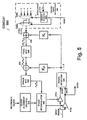
- Circuit 500 includes a CDR circuit that includes a phase detector 520, multiplier circuits K p and K i , sum circuits 530 and 550, a frequency ("freq") accumulator ("acc") 540, a phase acc 560, a clock alignment circuit 570 (such as a PLL/DLL circuit) and a phase interpolator 590.
- a square wave generator 580 that corresponds to jitter generator 430 outputs a jitter signal in the form of a square wave to sum circuit 530.
- Data and edge receivers 510a and 510b correspond to data/edge receivers 410.
- circuit 500 may be included in circuit 500, such as loop filters, equalizer circuits and de-serializer circuits.
- portions of circuit 500 are included in a digital circuit, such as a field programmable gate array ("FPGA") that outputs analog values by a digital-to-analog converter.
- FPGA field programmable gate array
- multiplier circuits K p and K i sum circuits 530 and 550, freq acc 540, phase acc 560, clock alignment circuit 570 and phase interpolator 590 may be included in a digital circuit.
- an input signal is sampled by data receiver 510a and edge receiver 510b, which output data and edge values in response to a data clock signal and an edge clock signal, respectively.
- Edge and data values are input to a phase detector 520 to determine the relative time/phase between the input signal and the receive clock signals and to output an up/down/hold signal to multiplier circuits K p and K i .
- an up/down/hold signal is a two bit digital signal represented as 1, -1, and 0 in 2's complement binary.
- Multiplier circuits K p and K i multiply the up/down/hold signals by respective constants (such as a proportional and integral constant) and outputs the products to inputs of sum circuits 550 and 530.
- Freq Acc 540 provides another input (a frequency signal) to sum circuit 550 that outputs a sum of the inputs to phase acc 560.
- Square wave generator 580 outputs a jitter signal to another input of sum circuit 530 that outputs a sum of the inputs to freq Acc 540.
- Phase acc 560 outputs a phase signal to phase interpolator circuit 590 in response to the output of sum circuit 550.
- Clock alignment circuit 570 may be a PLL or DLL circuit that provides a plurality of clock signals to a phase interpolator 590 in response to a reference clock signal.
- the reference clock signal may be provided external to circuit 500 or generated internally.
- Phase interpolator 590 outputs at least data and edge clock signals to data and edge receivers 510a-b in order to synchronize the sampling of the data and edge values. Inputting a jitter signal into sum circuit 530 enables at least one of the data and clock signals to be adjusted (or summed with a jitter signal) so that jitter tolerance may be measured.
- Square wave generator 580 outputs a jitter signal in the form of a square wave signal to sum circuit 530.
- This disturbance when passing through Freq acc 540 becomes a triangle wave.
- This triangle wave after passing through Phase acc 560 emulates approximately an SJ signal composed of parabolas.
- the receive clock signals are adjusted so that jitter tolerance may be measured.
- An amplitude and frequency of the approximate SJ signal may be determined by inputs to square wave generator 580.
- square wave generator 580 includes a binary counter 580a, a selector 580b, such as a multiplexer, and a multiplexer 580c for setting/disabling the test mode.
- Selector 580b outputs a selected constant value (C, -C, -C, C) as an input to sum circuit 530 in response to an output from binary counter 580a.
- Constant values (C, -C, -C, C) may be stored and output from a storage circuit or register in a control circuit, such as control 470.
- constant values (C, -C, -C, C) may be provided by an external source, such a controller or test equipment, during testing, initialization or during calibration mode of operation.
- the magnitude of C determines the amplitude of the SJ.
- An output of binary counter 580a is timed by a modulation clock..
- the relationship between the SJ frequency and the modulation clock frequency is determined by the 2 bits from the binary counter 580a that are used to control selector 580b. When the least significant two bits are used, the SJ frequency is 4 times slower than the modulation clock frequency. If an eight bit counter is used and the two most significant bits are used to control the selector 580b, then the SJ frequency is 1/256 times the modulation frequency.
- square wave generator 580 receives a reset signal from the control circuit in order to initiate the timing of the output of the jitter signal. For example, a reset signal may zero out or initialize binary counter 580a.
- This reset signal is used so as to avoid un-intentionally adding a frequency offset in addition to the SJ. Furthermore, the reset signal is input to multiplexer 580c to zero out the jitter input during normal operation. Accordingly, the constant values (C, -C, -C, C) determine the amplitude of the jitter signal and the binary counter output determines the frequency of the SJ signal caused by the square wave generator 580.
- Fig. 6 illustrates circuit 600 which is an exemplary embodiment of circuit 400.
- Circuit 600 includes similar circuits shown in Fig. 5 and operates similarly to circuit 500.
- circuit 600 includes a jitter circuit generator that includes binary counter 640, storage circuit 630, multiplier circuit A and sum circuit 610.
- Storage circuit 630 includes 2 N stored digital values representing a sinusoidal signal having predetermined amplitude. Digital sinusoidal values are output from storage circuit 630 in response to binary counter 640 that outputs the N bit address signal in response to a modulation clock.
- a decoder that uses the N bit address to select one entry from the storage at a time. How fast the digital values in storage circuit 630 are traversed (output) determines the frequency of the jitter signal (or SJ signal).
- An amplitude of the digital sinusoidal signal output from storage circuit 630 may be adjusted by applying a multiplier A whose output is modulo 1UI to the output of storage circuit 630.
- the amplitude or scalar of multiplier circuit A may be adjusted in response to a control signal from a control circuit, such as control 470 shown in Fig. 4 .
- Sum circuit 610 sums the output of multiplier circuit A and the output of phase acc 560 and provides a sum to clock alignment circuit 570. Accordingly, circuit 600 adjusts at least one of data and edge clock signals so that BER values for particular jitter signals having predetermined amplitude and frequency or tolerances may be measured.
- Circuits 500 and 600 are similar in that they can provide close to sinusoidal jitter signals having amplitudes of several UI that may be needed in tests that use low frequency SJ signals.
- circuit 600 generates other types of periodic jitter signals, such as square wave jitter, by only changing the contents of storage 630.
- Fig. 7 illustrates circuit 700 which is an exemplary embodiment of circuit 400.
- Circuit 700 includes similar circuits shown in Fig. 6 and operates similarly to circuit 600. However, circuit 700 includes a jitter circuit generator that outputs an RJ signal instead of an SJ signal.
- Circuit 700 includes a PRBS 710 instead of (or in addition to) the circuits that provide the SJ signal in circuits 500 and 600.
- An RJ signal is emulated by a PRBS 710 that outputs a predetermined random bit pattern/sequence (via sum circuit 610) to N least significant bits ("LSBs") of the output of phase acc 560.
- Sum circuit 610 outputs a sum of the output of phase acc 560 and the output of PRBS 710 (N LSBs) to phase interpolator 590.
- a number of LSBs (N) that will be modulated by the output of PRBS 710 may be determined by the intended amount of p2p RJ signal to be added.
- a control signal from a control circuit such as control 470, selects which N LSBs of the phase acc 560 the PRBS 710 output should be summed with.
- Fig. 8 illustrates circuit 800 which is an exemplary embodiment of circuit 400.
- Circuit 800 enables evaluation of the performance of an integrated circuit 801 including circuit 800 in the situation of a frequency offset between a transmitter 810 in another integrated circuit 802 and a receiver in integrated circuit 801 without actually causing such a frequency offset. In other words, the evaluation can be performed when the transmitter and the receiver of the input signal are using a same reference clock.
- Circuit 800 includes similar circuits shown in Fig. 7 and operates similarly to circuit 700. However, circuit 800 includes a constant C that forces a frequency offset at the input of phase acc 560 (via sum circuit 550) instead of an SJ and/or RJ signal.
- Circuit 700 includes a constant C instead of (or in addition to) the circuits that provide the SJ/RJ signals in circuits 500, 600 and 700.
- Constant C provides a selected frequency offset to an input of sum circuit 550 in response to a control signal that may be provided by a control circuit.
- the control signal may indicate the amount of frequency offset to be added.
- Fig. 9 illustrates a method 900 for evaluating an IC by adding jitter into at least one receive clock signal and/or measuring a BER value/jitter tolerance.
- logic blocks illustrated in Fig. 9 illustrate operations/functions of circuits, software or a user, singly or in combination.
- one or more circuits shown in Figs. 4-8 carry out method 900.
- Logic blocks that are not shown may be included in various embodiments; similarly, logic blocks that are shown may be excluded in various embodiments.
- method 900 is described in sequential logic blocks, logic blocks of method 900 may be completed concurrently in embodiments.
- Method 900 includes the steps of adding a controlled amount of jitter to at least one receive clock signal (901), sampling an input signal to generate sampled data values in response to the at least one receive clock signal (902), and evaluating the IC based on the sampled data values (903). In one embodiment, evaluating the IC includes computing a bit error ratio corresponding to the controlled amount of jitter. Method 900 may further include varying the amount of jitter (904) and repeating steps 901-903 with the varied amount of jitter.
- the IC includes a clock circuit for generating the at least one receive clock signal and the step of adding includes generating at least one jitter signal, and injecting the at least one jitter signal into a clock circuit.
- the at least one jitter signal may be one or more of a substantially square-wave signal, a substantially triangular wave signal, a digital/substantially sinusoidal signal, an emulated random jitter signal, a constant C signal, and any other suitable jitter signal.
- Each jitter signal has a controllable frequency and/or controllable amplitude, which may be varied in step 904.
- Integrated circuits described herein may be included in various systems or subsystems such as personal computers, graphics cards, set-top boxes, cable modems, cellular telephones, game consoles, digital television sets (for example, high definition television (“HDTV”)), fax machines, cable modems, digital versatile disc (“DVD”) players or network routers.
- Integrated circuits described herein may be housed in a variety of different types of packages having different types of external contacts.
- conductive paths described herein may include one or a plurality of wires and/or metal traces/regions/signal lines. Multiple conductive paths may replace a single conductive path illustrated in the figures and a single conductive path may replace multiple conductive paths illustrated in the figures.
- circuits disclosed herein may be described using computer aided design tools and expressed (or represented) as data and/or instructions embodied in various computer-readable media, in terms of their behavior, register transfer, logic component, transistor, layout geometries, and/or other characteristics.
- Formats of files and other objects in which such circuit expressions may be implemented include, but are not limited to: formats supporting behavioral languages such as C, Verilog, and HLDL; formats supporting register level description languages like RTL; formats supporting geometry description languages such as GDSII, GDSIII, GDSIV, CIF, MEBES; and any other suitable formats and languages.
- Computer-readable media in which such formatted data and/or instructions may be embodied include, but are not limited to, non-volatile storage media in various forms (e.g., optical, magnetic or semiconductor storage media) and carrier waves that may be used to transfer such formatted data and/or instructions through wireless, optical, or wired signaling media or any combination thereof.
- Examples of transfers of such formatted data and/or instructions by carrier waves include, but are not limited to, transfers (uploads, downloads, e-mail, etc.) over the Internet and/or other computer networks via one or more data transfer protocols (e.g., HTTP, FTP, SMTP, etc.).
- Such data and/or instruction-based expressions of the above described circuits may be processed by a processing entity (e.g., one or more processors) within the computer system in conjunction with execution of one or more other computer programs including, without limitation, netlist generation programs, place and route programs and the like, to generate a representation or image of a physical manifestation of such circuits.
- a processing entity e.g., one or more processors
- Such representation or image may thereafter be used in device fabrication, for example, by enabling generation of one or more masks that are used to form various components of the circuits in a device fabrication process.
Landscapes
- Physics & Mathematics (AREA)
- General Physics & Mathematics (AREA)
- Engineering & Computer Science (AREA)
- General Engineering & Computer Science (AREA)
- Nonlinear Science (AREA)
- Dc Digital Transmission (AREA)
- Manipulation Of Pulses (AREA)
- Tests Of Electronic Circuits (AREA)
Claims (15)
- Integrierte Schaltung (400), umfassend:eine Jittergeneratorschaltung (430), die ein Jittersignal erzeugt, das in mindestens ein Taktsignal eingefügt wird, wobei das Jitter-Signal kontrollierte Charakteristika hat; undeine Empfangsschaltung (410), die ein Eingangssignal gemäß des mindestens einen Taktsignals abtastet, wobei das Eingangssignal in die integrierte Schaltung (400) eingegeben wird und die Empfangsschaltung (410) abgetastete Datenwerte ausgibt, die zum Bestimmen einer Bitfehlerrate genutzt werden.
- Integrierte Schaltung (400) nach Anspruch 1, wobei das mindestens eine Taktsignal mindestens ein Datentaktsignal und mindestens ein Flankentaktsignal enthält, und wobei die Empfangsschaltung (410) umfasst:mindestens einen ersten Empfänger, der das Eingangssignal als Reaktion auf das mindestens eine Datentaktsignal abtastet; undmindestens einen zweiten Empfänger, der das Eingangssignal als Reaktion auf das mindestens eine Flankentaktsignal abtastet.
- Integrierte Schaltung (400) nach Anspruch 1, wobei die Jittergeneratorschaltung (430) das Jittersignal bereitstellt, indem es zumindest ein Jittersignal als Reaktion auf ein Kontrollsignal ausgibt, welches einen ersten Operationsmodus der integrierten Schaltung (400) vorgibt, wobei das mindestens eine Jittersignal jeweils eine oder eine Kombination aus einer vorgegebenen Frequenz, einer vorgegebenen Amplitude und einer vorgegebenen Wellenform hat, und
wobei die Jittergeneratorschaltung (430) die Ausgabe des mindestens einen Jittersignals als Reaktion auf ein Kontrollsignal stoppt, welches einen zweiten Operationsmodus der integrierten Schaltung (400) vorgibt. - Integrierte Schaltung (400) nach Anspruch 3, wobei das mindestens eine Jittersignal eines oder mehrere aus der folgenden Gruppe beinhaltet, die Gruppe bestehend aus: Einem im Wesentlichen rechteckwellenförmigen Signal, einem im Wesentlichen dreieckwellenförmigen Signal, einem im Wesentlichen sinusförmigen Signal, einem emulierten Zufallsjittersignal und einem Signal mit konstantem Frequenzversatz.
- Integrierte Schaltung (400) nach Anspruch 1, weiter umfassend eine Takt- und Datenrückgewinnungsschaltung (420), die zwischen die Jittergeneratorschaltung (430) und die Empfangsschaltung (410) gekoppelt ist, wobei die Takt- und Datenrückgewinnungsschaltung (420) das mindestens eine Taktsignal an die Empfangsschaltung (410) ausgibt.
- Integrierte Schaltung (400) nach Anspruch 5, wobei die Takt- und Datenrückgewinnungsschaltung (420) umfasst:einen Phasendetektor (520), der an die Empfangsschaltung (410) gekoppelt ist;einen Frequenzakkumulator (540), der an den Phasendetektor (520) gekoppelt ist; undeinen Phasenakkumulator (560), der an den Frequenzakkumulator (540) und den Phasendetektor (520) gekoppelt ist.
- Integrierte Schaltung (400) nach Anspruch 6, wobei die Takt- und Datenrückgewinnungsschaltung (420) eines oder mehrere aus der folgenden Gruppe beinhaltet, die Gruppe bestehen aus: Einem ersten Eingang zwischen dem Frequenzakkumulator (540) und dem Phasendetektor (520), einem zweiten Eingang zwischen dem Phasenakkumulator (560) und dem Frequenzakkumulator (540), und einem dritten Eingang zwischen dem Phasenakkumulator (560) und der Empfangsschaltung (410), und wobei die Jittergeneratorschaltung (430) das Jittersignal erzeugt, indem sie ein oder mehrere Jittersignale mit jeweils einer vorgegebenen Amplitude und einer vorgegebenen Frequenz in einen oder mehrere der ersten, zweiten und dritten Eingänge ausgibt, wodurch das Jittersignal in das mindestens eine Taktsignal eingefügt wird.
- Integrierte Schaltung (400) nach Anspruch 7, wobei die Takt- und Datenrückgewinnungsschaltung (420) eine oder mehrere einer ersten Summenschaltung, einer zweiten Summenschaltung und einer dritten Summenschaltung enthält, und wobei die ersten, zweiten und dritten Eingänge Eingänge der jeweiligen Schaltungen der ersten, zweiten und dritten Summenschaltungen sind.
- Integrierte Schaltung (400) nach Anspruch 1, weiter umfassend:einen Fehlerzähler, der mit der Empfangsschaltung (410) gekoppelt ist und einen Fehlerzählwert ausgibt, indem eine erwartete Menge an Datenwerten mit den abgetasteten Datenwerten verglichen wird, wobei der Fehlerzählerwert zum Berechnen der Bitfehlerrate benutzt wird.
- Integrierte Schaltung (500) nach Anspruch 1, weiter umfassend:eine Takt- und Datenrückgewinnungsschaltung (420), die abgetastete Datenwerte von der Empfangsschaltung (410) erhält und das mindestens eine Taktsignal ausgibt; undwobei die Jittergeneratorschaltung (430) das mindestens eine Jittersignal an die Takt- und Datenrückgewinnungsschaltung (420) ausgibt, so dass das mindestens eine Taktsignal einen kontrollierten Betrag an Jitter hat.
- Integrierte Schaltung (500) nach Anspruch 10, wobei die Takt- und Datenrückgewinnungsschaltung (420) einen Phasendetektor (520), einen Frequenzakkumulator (540) und eine Summenschaltung, welche einen ersten Eingang, der mit dem Phasendetektor (520) gekoppelt ist, einen Ausgang, der mit dem Frequenzakkumulator (540) gekoppelt ist und einen zweiten Eingang hat, enthält, und wobei die Jittergeneratorschaltung (430) umfasst:eine Rechtecksignalgeneratorschaltung, die dem zweiten Eingang der Summenschaltung ein Rechtecksignal bereitstellt.
- Integrierte Schaltung (500) nach Anspruch 10, wobei die Jittergeneratorschaltung (430) umfasst:einen Binärzähler, der einen Zählwert ausgibt;eine Speicherschaltung, die mindestens einen Wert als Reaktion auf den Zählwert ausgibt: undeine Multiplikationsschaltung, die ein Produktsignal, das auf dem mindestens einen Wert und einem konstanten Wert basiert, ausgibt.
- Integrierte Schaltung (500) nach Anspruch 10, wobei die Takt- und Datenrückgewinnungsschaltung (420) einen Phasenakkumulator (560) mit einem Ausgang enthält und die Jittergeneratorschaltung (430) umfasst:eine Pseudozufallsbitsequenz-Schaltung, die ein zufälliges Jittersignal, das aus N Bits besteht, ausgibt, welches zu den niederwertigsten Bits der Ausgabe des Phasenakkumulators (560) addiert wird.
- Verfahren zur Evaluierung einer integrierten Schaltung (400), umfassend:Addieren eines kontrollierten Betrags an Jitter zu mindestens einem Empfangstaktsignal, wobei der kontrollierte Betrag an Jitter on-chip generiert wird;Abtasten eines Eingangssignals, so dass abgetastete Datenwerte generiert werden, als Reaktion auf das mindestens eine Empfangstaktsignal, wobei das Eingangssignal in die integrierte Schaltung (400) eingegeben wird; undBerechnen einer Bitfehlerrate auf Basis der abgetasteten Datenwerte und einer erwarteten Menge an Datenwerten.
- Verfahren nach Anspruch 14, wobei der kontrollierte Betrag an Jitter von mindestens einem ersten Jittersignal abgeleitet ist, das zumindest eine kontrollierbare Frequenz oder eine kontrollierte Amplitude besitzt, wobei das Verfahren weiter das Verändern zumindest der kontrollierten Frequenz oder der kontrollierten Amplitude des mindestens einen Jittersignals umfasst.
Priority Applications (1)
| Application Number | Priority Date | Filing Date | Title |
|---|---|---|---|
| EP11165959A EP2360488B1 (de) | 2007-03-20 | 2008-03-19 | Integrierte Schaltung mit Empfängerjittertoleranzmessung |
Applications Claiming Priority (2)
| Application Number | Priority Date | Filing Date | Title |
|---|---|---|---|
| US89586007P | 2007-03-20 | 2007-03-20 | |
| PCT/US2008/057455 WO2008115968A1 (en) | 2007-03-20 | 2008-03-19 | Integrated circuit having receiver jitter tolerance ('jtol') measurement |
Publications (2)
| Publication Number | Publication Date |
|---|---|
| EP2130055A1 EP2130055A1 (de) | 2009-12-09 |
| EP2130055B1 true EP2130055B1 (de) | 2011-05-18 |
Family
ID=39589250
Family Applications (2)
| Application Number | Title | Priority Date | Filing Date |
|---|---|---|---|
| EP08744054A Active EP2130055B1 (de) | 2007-03-20 | 2008-03-19 | Integrierte schaltung mit empfängerjittertoleranzmessung |
| EP11165959A Active EP2360488B1 (de) | 2007-03-20 | 2008-03-19 | Integrierte Schaltung mit Empfängerjittertoleranzmessung |
Family Applications After (1)
| Application Number | Title | Priority Date | Filing Date |
|---|---|---|---|
| EP11165959A Active EP2360488B1 (de) | 2007-03-20 | 2008-03-19 | Integrierte Schaltung mit Empfängerjittertoleranzmessung |
Country Status (5)
| Country | Link |
|---|---|
| US (6) | US8289032B2 (de) |
| EP (2) | EP2130055B1 (de) |
| JP (1) | JP5432730B2 (de) |
| AT (1) | ATE510225T1 (de) |
| WO (1) | WO2008115968A1 (de) |
Families Citing this family (49)
| Publication number | Priority date | Publication date | Assignee | Title |
|---|---|---|---|---|
| US20050071707A1 (en) | 2003-09-30 | 2005-03-31 | Hampel Craig E. | Integrated circuit with bi-modal data strobe |
| ATE510225T1 (de) | 2007-03-20 | 2011-06-15 | Rambus Inc | Integrierte schaltung mit empfängerjittertoleranzmessung |
| US8509295B1 (en) * | 2008-09-04 | 2013-08-13 | Marvell Israel (M.I.S.L) Ltd. | Bit error rate prediction |
| WO2010059331A1 (en) * | 2008-11-20 | 2010-05-27 | Rambus Inc. | Jitter correction in high speed data link |
| US8804888B2 (en) * | 2010-07-12 | 2014-08-12 | Ensphere Solutions, Inc. | Wide band clock data recovery |
| US9222972B1 (en) * | 2010-09-17 | 2015-12-29 | Altera Corporation | On-die jitter generator |
| US8634509B2 (en) * | 2011-02-15 | 2014-01-21 | Cavium, Inc. | Synchronized clock phase interpolator |
| TWI444636B (zh) * | 2011-02-18 | 2014-07-11 | Realtek Semiconductor Corp | 內建抖動測試功能之時脈與資料回復電路及其方法 |
| US8760188B2 (en) * | 2011-06-30 | 2014-06-24 | Silicon Image, Inc. | Configurable multi-dimensional driver and receiver |
| US9071243B2 (en) | 2011-06-30 | 2015-06-30 | Silicon Image, Inc. | Single ended configurable multi-mode driver |
| US8687755B1 (en) * | 2012-01-31 | 2014-04-01 | Altera Corporation | Interpolator-based clock and data recovery with reduced quantization error |
| WO2013137863A1 (en) | 2012-03-13 | 2013-09-19 | Rambus Inc. | Clock and data recovery having shared clock generator |
| JP5809590B2 (ja) | 2012-03-21 | 2015-11-11 | 株式会社アドバンテスト | 信号発生装置および信号発生方法 |
| US9071407B2 (en) | 2012-05-02 | 2015-06-30 | Ramnus Inc. | Receiver clock test circuitry and related methods and apparatuses |
| US8923375B2 (en) | 2012-06-29 | 2014-12-30 | Parade Technologies, Inc. | On die jitter tolerance test |
| US9952276B2 (en) | 2013-02-21 | 2018-04-24 | Advantest Corporation | Tester with mixed protocol engine in a FPGA block |
| US10161993B2 (en) * | 2013-02-21 | 2018-12-25 | Advantest Corporation | Tester with acceleration on memory and acceleration for automatic pattern generation within a FPGA block |
| US10162007B2 (en) | 2013-02-21 | 2018-12-25 | Advantest Corporation | Test architecture having multiple FPGA based hardware accelerator blocks for testing multiple DUTs independently |
| US11009550B2 (en) | 2013-02-21 | 2021-05-18 | Advantest Corporation | Test architecture with an FPGA based test board to simulate a DUT or end-point |
| JP2014174131A (ja) * | 2013-03-13 | 2014-09-22 | Fujitsu Semiconductor Ltd | 受信回路、半導体集積回路及び試験方法 |
| JP6032080B2 (ja) * | 2013-03-22 | 2016-11-24 | 富士通株式会社 | 受信回路及び受信回路の制御方法 |
| JP6127635B2 (ja) * | 2013-03-25 | 2017-05-17 | 富士通株式会社 | 受信回路および通信回路 |
| JP6149594B2 (ja) * | 2013-08-09 | 2017-06-21 | 富士通株式会社 | 受信回路 |
| US9065653B2 (en) * | 2013-11-01 | 2015-06-23 | Korea Advanced Institute Of Science & Technology | Internal jitter tolerance tester with an internal jitter generator |
| EP3080675A4 (de) * | 2013-12-13 | 2017-09-27 | Intel Corporation | Datenempfängerschaltung mit probennehmern mit versetzten kanten |
| US9088399B1 (en) * | 2014-02-03 | 2015-07-21 | Xilinx, Inc. | Circuit and method for testing jitter tolerance |
| KR101518172B1 (ko) * | 2014-05-16 | 2015-05-11 | 인하대학교 산학협력단 | Cdr 성능 평가를 위한 온 칩 지터톨러런스 측정 방법 및 장치 |
| US9898565B2 (en) | 2015-11-25 | 2018-02-20 | Synopsys, Inc. | Clock jitter emulation |
| US9590640B1 (en) * | 2015-12-16 | 2017-03-07 | Realtek Semiconductor Corporation | Clock and data recovery apparatus and method of the same |
| JP6839359B2 (ja) * | 2017-04-28 | 2021-03-10 | 富士通株式会社 | ジッタ測定回路 |
| US10038545B1 (en) * | 2017-07-26 | 2018-07-31 | Xilinx, Inc. | Systems and methods for clock and data recovery |
| KR102410014B1 (ko) * | 2017-08-03 | 2022-06-21 | 삼성전자주식회사 | 클락 지터 측정 회로 및 이를 포함하는 반도체 장치 |
| US10802074B2 (en) * | 2018-01-02 | 2020-10-13 | Jitterlabs Llc | Method and apparatus for analyzing phase noise in a signal from an electronic device |
| US11714127B2 (en) | 2018-06-12 | 2023-08-01 | International Business Machines Corporation | On-chip spread spectrum characterization |
| US10693589B2 (en) | 2018-06-18 | 2020-06-23 | Huawei Technologies Co., Ltd. | Serdes with jitter injection self stress mechanism |
| KR102691396B1 (ko) | 2018-11-22 | 2024-08-06 | 삼성전자주식회사 | 데이터를 복원하기 위한 샘플링 타이밍을 조절하도록 구성되는 전자 회로 |
| US10897275B2 (en) * | 2018-12-27 | 2021-01-19 | Intel Corporation | Polar modulation systems and methods |
| JP7217204B2 (ja) * | 2019-06-28 | 2023-02-02 | 株式会社アドバンテスト | 信号処理装置および信号処理方法 |
| US11146307B1 (en) * | 2020-04-13 | 2021-10-12 | International Business Machines Corporation | Detecting distortion in spread spectrum signals |
| KR20220091880A (ko) | 2020-12-24 | 2022-07-01 | 삼성전자주식회사 | 위상 보간 기반의 클럭 데이터 복원 회로 및 이를 포함하는 통신 장치 |
| US11784856B2 (en) * | 2021-01-22 | 2023-10-10 | Macom Technology Solutions Holdings, Inc. | Area efficient high-speed sequence generator and error checker |
| US11948621B2 (en) * | 2021-07-28 | 2024-04-02 | Samsung Electronics Co., Ltd. | Memory devices, memory systems having the same, and operating methods thereof |
| KR102833443B1 (ko) | 2021-09-13 | 2025-07-10 | 삼성전자주식회사 | 패턴 생성기 및 이를 포함하는 내장 자체 시험 장치 |
| US11693446B2 (en) | 2021-10-20 | 2023-07-04 | International Business Machines Corporation | On-chip spread spectrum synchronization between spread spectrum sources |
| US11803437B1 (en) * | 2022-06-30 | 2023-10-31 | Advanced Micro Devices, Inc. | Write hardware training acceleration |
| US12235318B2 (en) | 2022-07-12 | 2025-02-25 | Samsung Electronics Co., Ltd. | Methods for determining and calibrating non-linearity in a Phase Interpolator and related devices and systems |
| US12160494B2 (en) * | 2023-05-01 | 2024-12-03 | Bae Systems Information And Electronic Systems Integration Inc. | Non-integer interpolation for signal sampling at asynchronous clock rates |
| CN119339751A (zh) * | 2023-07-19 | 2025-01-21 | 美光科技公司 | 基于错误率的电压缩放 |
| US12596148B1 (en) * | 2024-10-09 | 2026-04-07 | Nvidia Corporation | Jitter injection generator for measuring phase noise and jitter transfer function |
Family Cites Families (34)
| Publication number | Priority date | Publication date | Assignee | Title |
|---|---|---|---|---|
| US5394106A (en) * | 1993-08-31 | 1995-02-28 | Gadzoox Microsystems | Apparatus and method for synthesis of signals with programmable periods |
| US5481563A (en) * | 1994-03-14 | 1996-01-02 | Network Systems Corporation | Jitter measurement using a statistically locked loop |
| US5654657A (en) * | 1995-08-01 | 1997-08-05 | Schlumberger Technologies Inc. | Accurate alignment of clocks in mixed-signal tester |
| US5793822A (en) * | 1995-10-16 | 1998-08-11 | Symbios, Inc. | Bist jitter tolerance measurement technique |
| FR2775789B1 (fr) * | 1998-03-09 | 2001-10-12 | Sgs Thomson Microelectronics | Test numerique de signal periodique |
| US6285726B1 (en) * | 1998-05-18 | 2001-09-04 | National Semiconductor Corporation | 10/100 mb clock recovery architecture for switches, repeaters and multi-physical layer ports |
| US6760389B1 (en) * | 1998-06-01 | 2004-07-06 | Agere Systems Inc. | Data recovery for non-uniformly spaced edges |
| DE19913722C1 (de) * | 1999-03-26 | 2000-10-26 | Wandel & Goltermann Management | Verfahren und Vorrichtung zum Prüfen eines Jittergenerators |
| US6718497B1 (en) | 2000-04-21 | 2004-04-06 | Apple Computer, Inc. | Method and apparatus for generating jitter test patterns on a high performance serial bus |
| US7642566B2 (en) * | 2006-06-12 | 2010-01-05 | Dsm Solutions, Inc. | Scalable process and structure of JFET for small and decreasing line widths |
| US6874107B2 (en) * | 2001-07-24 | 2005-03-29 | Xilinx, Inc. | Integrated testing of serializer/deserializer in FPGA |
| WO2003073115A1 (fr) * | 2002-02-26 | 2003-09-04 | Advantest Corporation | Instrument et procede de mesure |
| WO2003073280A1 (en) * | 2002-02-26 | 2003-09-04 | Advantest Corporation | Measuring apparatus and measuring method |
| WO2003076959A1 (fr) * | 2002-03-08 | 2003-09-18 | Advantest Corporation | Dispositif testeur a semi-conducteur et procede de mesure de synchronisation pour ce dispositif |
| JP4006260B2 (ja) * | 2002-04-26 | 2007-11-14 | 株式会社アドバンテスト | 半導体試験装置 |
| US7397848B2 (en) * | 2003-04-09 | 2008-07-08 | Rambus Inc. | Partial response receiver |
| US7092472B2 (en) * | 2003-09-16 | 2006-08-15 | Rambus Inc. | Data-level clock recovery |
| US7230981B2 (en) * | 2003-05-09 | 2007-06-12 | Stmicroelectronics, Inc. | Integrated data jitter generator for the testing of high-speed serial interfaces |
| US7136773B2 (en) * | 2003-12-16 | 2006-11-14 | Advantest Corporation | Testing apparatus and testing method |
| JP2005233933A (ja) | 2004-01-19 | 2005-09-02 | Nec Electronics Corp | 組合せ試験方法及び試験装置 |
| US20050193290A1 (en) * | 2004-02-25 | 2005-09-01 | Cho James B. | Built-in self test method and apparatus for jitter transfer, jitter tolerance, and FIFO data buffer |
| US7246274B2 (en) * | 2004-09-10 | 2007-07-17 | Rambus Inc. | Method and apparatus for estimating random jitter (RJ) and deterministic jitter (DJ) from bit error rate (BER) |
| JP4621050B2 (ja) * | 2005-03-28 | 2011-01-26 | 株式会社アドバンテスト | クロック乗替装置、及び試験装置 |
| US20060247906A1 (en) * | 2005-04-27 | 2006-11-02 | International Business Machines Corporation | Method for estimating clock jitter for static timing measurements of modeled circuits |
| US7562271B2 (en) | 2005-09-26 | 2009-07-14 | Rambus Inc. | Memory system topologies including a buffer device and an integrated circuit memory device |
| US7596173B2 (en) * | 2005-10-28 | 2009-09-29 | Advantest Corporation | Test apparatus, clock generator and electronic device |
| US7668235B2 (en) * | 2005-11-10 | 2010-02-23 | Teradyne | Jitter measurement algorithm using locally in-order strobes |
| FR2899404A1 (fr) * | 2006-03-28 | 2007-10-05 | St Microelectronics Sa | Estimation de gigue d'un signal d'horloge |
| US8570881B2 (en) * | 2006-03-28 | 2013-10-29 | Advanced Micro Devices, Inc. | Transmitter voltage and receiver time margining |
| JPWO2008032701A1 (ja) * | 2006-09-13 | 2010-01-28 | 日本電気株式会社 | クロック調整回路と半導体集積回路装置 |
| US7952516B2 (en) * | 2006-09-26 | 2011-05-31 | Lockheed Martin Corporation | System and method for coherent frequency switching in DDS architectures |
| CN101207472B (zh) * | 2006-12-20 | 2012-03-14 | 国际商业机器公司 | 同步时钟信道和数据信道信号的通信系统及接收器和方法 |
| US8045605B2 (en) * | 2006-12-25 | 2011-10-25 | Advantest Corporation | Jitter amplifier circuit, signal generation circuit, semiconductor chip, and test apparatus |
| ATE510225T1 (de) * | 2007-03-20 | 2011-06-15 | Rambus Inc | Integrierte schaltung mit empfängerjittertoleranzmessung |
-
2008
- 2008-03-19 AT AT08744054T patent/ATE510225T1/de not_active IP Right Cessation
- 2008-03-19 EP EP08744054A patent/EP2130055B1/de active Active
- 2008-03-19 EP EP11165959A patent/EP2360488B1/de active Active
- 2008-03-19 WO PCT/US2008/057455 patent/WO2008115968A1/en not_active Ceased
- 2008-03-19 JP JP2009554706A patent/JP5432730B2/ja active Active
- 2008-03-19 US US12/529,320 patent/US8289032B2/en not_active Expired - Fee Related
-
2012
- 2012-09-17 US US13/621,783 patent/US9423441B2/en active Active
-
2016
- 2016-07-13 US US15/209,494 patent/US9791492B2/en active Active
-
2017
- 2017-09-08 US US15/699,874 patent/US10466289B2/en active Active
-
2019
- 2019-10-28 US US16/665,179 patent/US11022639B2/en active Active
-
2021
- 2021-04-27 US US17/241,660 patent/US11525854B2/en active Active
Also Published As
| Publication number | Publication date |
|---|---|
| US9791492B2 (en) | 2017-10-17 |
| US8289032B2 (en) | 2012-10-16 |
| JP5432730B2 (ja) | 2014-03-05 |
| US20130093433A1 (en) | 2013-04-18 |
| EP2130055A1 (de) | 2009-12-09 |
| US20200124652A1 (en) | 2020-04-23 |
| US20180052194A1 (en) | 2018-02-22 |
| US20170052221A1 (en) | 2017-02-23 |
| US11022639B2 (en) | 2021-06-01 |
| US11525854B2 (en) | 2022-12-13 |
| EP2360488B1 (de) | 2013-01-23 |
| US10466289B2 (en) | 2019-11-05 |
| EP2360488A1 (de) | 2011-08-24 |
| ATE510225T1 (de) | 2011-06-15 |
| US20100097071A1 (en) | 2010-04-22 |
| WO2008115968A1 (en) | 2008-09-25 |
| JP2010522331A (ja) | 2010-07-01 |
| US20210318371A1 (en) | 2021-10-14 |
| US9423441B2 (en) | 2016-08-23 |
Similar Documents
| Publication | Publication Date | Title |
|---|---|---|
| EP2130055B1 (de) | Integrierte schaltung mit empfängerjittertoleranzmessung | |
| US7363563B1 (en) | Systems and methods for a built in test circuit for asynchronous testing of high-speed transceivers | |
| US8504882B2 (en) | Circuitry on an integrated circuit for performing or facilitating oscilloscope, jitter, and/or bit-error-rate tester operations | |
| WO2007099918A1 (ja) | 測定装置、試験装置、及び電子デバイス | |
| EP1815262B1 (de) | System und verfahren zur jitter-einspeisung auf dem chip | |
| EP1730539A2 (de) | Verfahren und vorrichtung für eingebaute selbstprüfung für jitter-transfer, jitter-toleranz und fifo-datenpuffer | |
| US8514920B2 (en) | Methods and apparatus for pseudo asynchronous testing of receive path in serializer/deserializer devices | |
| EP2603805A2 (de) | Schaltung in einem integrierten schaltkreis zur durchführung oder erleichterung des betriebs eines oszilloskops, eines jitters und/oder eines bitfehlerraten-testers | |
| US20230184828A1 (en) | Method and Apparatus for Analyzing Phase Noise in a Signal from an Electronic Device | |
| JP6346212B2 (ja) | 誤り率測定装置及び該装置を用いた自動位相調整方法 | |
| TWI400460B (zh) | 傳輸延遲與顫動量測方法 | |
| JP5410454B2 (ja) | パルスパターン発生装置及び該装置を用いた誤り率測定システム並びにパルスパターン発生方法 | |
| TW202440030A (zh) | 眼距測試方法及基於此方法進行測試操作的電子設備 | |
| JP2005181325A (ja) | 試験装置、及び試験方法 | |
| Damm | Jitter–An Introduction | |
| Hong | Efficient test methodologies for high-speed serial links | |
| Werner et al. | Modeling, simulation, and design of a multi-mode 2-10 Gb/sec fully adaptive serial link system | |
| DiCecco et al. | Test considerations for jitter tolerance of wireline receivers | |
| Kamm et al. | SerDes interoperability and optimization | |
| Jin et al. | A 4Gb/s/link Differential Bidirectional Serial Interface with Self-Diagnosis |
Legal Events
| Date | Code | Title | Description |
|---|---|---|---|
| PUAI | Public reference made under article 153(3) epc to a published international application that has entered the european phase |
Free format text: ORIGINAL CODE: 0009012 |
|
| 17P | Request for examination filed |
Effective date: 20091020 |
|
| AK | Designated contracting states |
Kind code of ref document: A1 Designated state(s): AT BE BG CH CY CZ DE DK EE ES FI FR GB GR HR HU IE IS IT LI LT LU LV MC MT NL NO PL PT RO SE SI SK TR |
|
| 17Q | First examination report despatched |
Effective date: 20100217 |
|
| DAX | Request for extension of the european patent (deleted) | ||
| GRAP | Despatch of communication of intention to grant a patent |
Free format text: ORIGINAL CODE: EPIDOSNIGR1 |
|
| RAP1 | Party data changed (applicant data changed or rights of an application transferred) |
Owner name: RAMBUS INC. |
|
| GRAS | Grant fee paid |
Free format text: ORIGINAL CODE: EPIDOSNIGR3 |
|
| GRAA | (expected) grant |
Free format text: ORIGINAL CODE: 0009210 |
|
| REG | Reference to a national code |
Ref country code: GB Ref legal event code: FG4D |
|
| REG | Reference to a national code |
Ref country code: CH Ref legal event code: EP |
|
| REG | Reference to a national code |
Ref country code: IE Ref legal event code: FG4D |
|
| REG | Reference to a national code |
Ref country code: DE Ref legal event code: R096 Ref document number: 602008007017 Country of ref document: DE Effective date: 20110630 |
|
| REG | Reference to a national code |
Ref country code: NL Ref legal event code: VDEP Effective date: 20110518 |
|
| PG25 | Lapsed in a contracting state [announced via postgrant information from national office to epo] |
Ref country code: HR Free format text: LAPSE BECAUSE OF FAILURE TO SUBMIT A TRANSLATION OF THE DESCRIPTION OR TO PAY THE FEE WITHIN THE PRESCRIBED TIME-LIMIT Effective date: 20110518 Ref country code: PT Free format text: LAPSE BECAUSE OF FAILURE TO SUBMIT A TRANSLATION OF THE DESCRIPTION OR TO PAY THE FEE WITHIN THE PRESCRIBED TIME-LIMIT Effective date: 20110919 Ref country code: SE Free format text: LAPSE BECAUSE OF FAILURE TO SUBMIT A TRANSLATION OF THE DESCRIPTION OR TO PAY THE FEE WITHIN THE PRESCRIBED TIME-LIMIT Effective date: 20110518 Ref country code: LT Free format text: LAPSE BECAUSE OF FAILURE TO SUBMIT A TRANSLATION OF THE DESCRIPTION OR TO PAY THE FEE WITHIN THE PRESCRIBED TIME-LIMIT Effective date: 20110518 Ref country code: NO Free format text: LAPSE BECAUSE OF FAILURE TO SUBMIT A TRANSLATION OF THE DESCRIPTION OR TO PAY THE FEE WITHIN THE PRESCRIBED TIME-LIMIT Effective date: 20110818 |
|
| PG25 | Lapsed in a contracting state [announced via postgrant information from national office to epo] |
Ref country code: LV Free format text: LAPSE BECAUSE OF FAILURE TO SUBMIT A TRANSLATION OF THE DESCRIPTION OR TO PAY THE FEE WITHIN THE PRESCRIBED TIME-LIMIT Effective date: 20110518 Ref country code: BE Free format text: LAPSE BECAUSE OF FAILURE TO SUBMIT A TRANSLATION OF THE DESCRIPTION OR TO PAY THE FEE WITHIN THE PRESCRIBED TIME-LIMIT Effective date: 20110518 Ref country code: ES Free format text: LAPSE BECAUSE OF FAILURE TO SUBMIT A TRANSLATION OF THE DESCRIPTION OR TO PAY THE FEE WITHIN THE PRESCRIBED TIME-LIMIT Effective date: 20110829 Ref country code: IS Free format text: LAPSE BECAUSE OF FAILURE TO SUBMIT A TRANSLATION OF THE DESCRIPTION OR TO PAY THE FEE WITHIN THE PRESCRIBED TIME-LIMIT Effective date: 20110918 Ref country code: FI Free format text: LAPSE BECAUSE OF FAILURE TO SUBMIT A TRANSLATION OF THE DESCRIPTION OR TO PAY THE FEE WITHIN THE PRESCRIBED TIME-LIMIT Effective date: 20110518 Ref country code: GR Free format text: LAPSE BECAUSE OF FAILURE TO SUBMIT A TRANSLATION OF THE DESCRIPTION OR TO PAY THE FEE WITHIN THE PRESCRIBED TIME-LIMIT Effective date: 20110819 Ref country code: SI Free format text: LAPSE BECAUSE OF FAILURE TO SUBMIT A TRANSLATION OF THE DESCRIPTION OR TO PAY THE FEE WITHIN THE PRESCRIBED TIME-LIMIT Effective date: 20110518 Ref country code: AT Free format text: LAPSE BECAUSE OF FAILURE TO SUBMIT A TRANSLATION OF THE DESCRIPTION OR TO PAY THE FEE WITHIN THE PRESCRIBED TIME-LIMIT Effective date: 20110518 Ref country code: CY Free format text: LAPSE BECAUSE OF FAILURE TO SUBMIT A TRANSLATION OF THE DESCRIPTION OR TO PAY THE FEE WITHIN THE PRESCRIBED TIME-LIMIT Effective date: 20110518 |
|
| PG25 | Lapsed in a contracting state [announced via postgrant information from national office to epo] |
Ref country code: NL Free format text: LAPSE BECAUSE OF FAILURE TO SUBMIT A TRANSLATION OF THE DESCRIPTION OR TO PAY THE FEE WITHIN THE PRESCRIBED TIME-LIMIT Effective date: 20110518 |
|
| PG25 | Lapsed in a contracting state [announced via postgrant information from national office to epo] |
Ref country code: CZ Free format text: LAPSE BECAUSE OF FAILURE TO SUBMIT A TRANSLATION OF THE DESCRIPTION OR TO PAY THE FEE WITHIN THE PRESCRIBED TIME-LIMIT Effective date: 20110518 Ref country code: EE Free format text: LAPSE BECAUSE OF FAILURE TO SUBMIT A TRANSLATION OF THE DESCRIPTION OR TO PAY THE FEE WITHIN THE PRESCRIBED TIME-LIMIT Effective date: 20110518 |
|
| PG25 | Lapsed in a contracting state [announced via postgrant information from national office to epo] |
Ref country code: RO Free format text: LAPSE BECAUSE OF FAILURE TO SUBMIT A TRANSLATION OF THE DESCRIPTION OR TO PAY THE FEE WITHIN THE PRESCRIBED TIME-LIMIT Effective date: 20110518 Ref country code: PL Free format text: LAPSE BECAUSE OF FAILURE TO SUBMIT A TRANSLATION OF THE DESCRIPTION OR TO PAY THE FEE WITHIN THE PRESCRIBED TIME-LIMIT Effective date: 20110518 Ref country code: DK Free format text: LAPSE BECAUSE OF FAILURE TO SUBMIT A TRANSLATION OF THE DESCRIPTION OR TO PAY THE FEE WITHIN THE PRESCRIBED TIME-LIMIT Effective date: 20110518 Ref country code: SK Free format text: LAPSE BECAUSE OF FAILURE TO SUBMIT A TRANSLATION OF THE DESCRIPTION OR TO PAY THE FEE WITHIN THE PRESCRIBED TIME-LIMIT Effective date: 20110518 |
|
| PLBE | No opposition filed within time limit |
Free format text: ORIGINAL CODE: 0009261 |
|
| STAA | Information on the status of an ep patent application or granted ep patent |
Free format text: STATUS: NO OPPOSITION FILED WITHIN TIME LIMIT |
|
| 26N | No opposition filed |
Effective date: 20120221 |
|
| PG25 | Lapsed in a contracting state [announced via postgrant information from national office to epo] |
Ref country code: IT Free format text: LAPSE BECAUSE OF FAILURE TO SUBMIT A TRANSLATION OF THE DESCRIPTION OR TO PAY THE FEE WITHIN THE PRESCRIBED TIME-LIMIT Effective date: 20110518 |
|
| REG | Reference to a national code |
Ref country code: DE Ref legal event code: R097 Ref document number: 602008007017 Country of ref document: DE Effective date: 20120221 |
|
| PG25 | Lapsed in a contracting state [announced via postgrant information from national office to epo] |
Ref country code: MC Free format text: LAPSE BECAUSE OF NON-PAYMENT OF DUE FEES Effective date: 20120331 |
|
| REG | Reference to a national code |
Ref country code: CH Ref legal event code: PL |
|
| REG | Reference to a national code |
Ref country code: IE Ref legal event code: MM4A |
|
| PG25 | Lapsed in a contracting state [announced via postgrant information from national office to epo] |
Ref country code: IE Free format text: LAPSE BECAUSE OF NON-PAYMENT OF DUE FEES Effective date: 20120319 Ref country code: CH Free format text: LAPSE BECAUSE OF NON-PAYMENT OF DUE FEES Effective date: 20120331 Ref country code: LI Free format text: LAPSE BECAUSE OF NON-PAYMENT OF DUE FEES Effective date: 20120331 |
|
| PG25 | Lapsed in a contracting state [announced via postgrant information from national office to epo] |
Ref country code: BG Free format text: LAPSE BECAUSE OF FAILURE TO SUBMIT A TRANSLATION OF THE DESCRIPTION OR TO PAY THE FEE WITHIN THE PRESCRIBED TIME-LIMIT Effective date: 20110818 |
|
| PG25 | Lapsed in a contracting state [announced via postgrant information from national office to epo] |
Ref country code: MT Free format text: LAPSE BECAUSE OF FAILURE TO SUBMIT A TRANSLATION OF THE DESCRIPTION OR TO PAY THE FEE WITHIN THE PRESCRIBED TIME-LIMIT Effective date: 20110518 |
|
| PG25 | Lapsed in a contracting state [announced via postgrant information from national office to epo] |
Ref country code: TR Free format text: LAPSE BECAUSE OF FAILURE TO SUBMIT A TRANSLATION OF THE DESCRIPTION OR TO PAY THE FEE WITHIN THE PRESCRIBED TIME-LIMIT Effective date: 20110518 |
|
| PG25 | Lapsed in a contracting state [announced via postgrant information from national office to epo] |
Ref country code: LU Free format text: LAPSE BECAUSE OF NON-PAYMENT OF DUE FEES Effective date: 20120319 |
|
| PGFP | Annual fee paid to national office [announced via postgrant information from national office to epo] |
Ref country code: FR Payment date: 20140317 Year of fee payment: 7 |
|
| PG25 | Lapsed in a contracting state [announced via postgrant information from national office to epo] |
Ref country code: HU Free format text: LAPSE BECAUSE OF FAILURE TO SUBMIT A TRANSLATION OF THE DESCRIPTION OR TO PAY THE FEE WITHIN THE PRESCRIBED TIME-LIMIT Effective date: 20080319 |
|
| REG | Reference to a national code |
Ref country code: FR Ref legal event code: ST Effective date: 20151130 |
|
| PG25 | Lapsed in a contracting state [announced via postgrant information from national office to epo] |
Ref country code: FR Free format text: LAPSE BECAUSE OF NON-PAYMENT OF DUE FEES Effective date: 20150331 |
|
| REG | Reference to a national code |
Ref country code: DE Ref legal event code: R082 Ref document number: 602008007017 Country of ref document: DE Representative=s name: EISENFUEHR SPEISER PATENTANWAELTE RECHTSANWAEL, DE Ref country code: DE Ref legal event code: R081 Ref document number: 602008007017 Country of ref document: DE Owner name: RAMBUS INC. (N.D.GES. DES STAATES DELAWARE), S, US Free format text: FORMER OWNER: RAMBUS INC., SUNNYVALE, CALIF., US |
|
| PGFP | Annual fee paid to national office [announced via postgrant information from national office to epo] |
Ref country code: GB Payment date: 20260327 Year of fee payment: 19 |
|
| PGFP | Annual fee paid to national office [announced via postgrant information from national office to epo] |
Ref country code: DE Payment date: 20260327 Year of fee payment: 19 |