EP2141741A2 - Elektronischer Schaltkreis mit einem MOS-Transistor in Diodenschaltung mit verbessertem Wirkungsgrad - Google Patents
Elektronischer Schaltkreis mit einem MOS-Transistor in Diodenschaltung mit verbessertem Wirkungsgrad Download PDFInfo
- Publication number
- EP2141741A2 EP2141741A2 EP09164596A EP09164596A EP2141741A2 EP 2141741 A2 EP2141741 A2 EP 2141741A2 EP 09164596 A EP09164596 A EP 09164596A EP 09164596 A EP09164596 A EP 09164596A EP 2141741 A2 EP2141741 A2 EP 2141741A2
- Authority
- EP
- European Patent Office
- Prior art keywords
- transistor
- diode
- power terminal
- source
- mos transistor
- Prior art date
- Legal status (The legal status is an assumption and is not a legal conclusion. Google has not performed a legal analysis and makes no representation as to the accuracy of the status listed.)
- Withdrawn
Links
Images


Classifications
-
- H—ELECTRICITY
- H10—SEMICONDUCTOR DEVICES; ELECTRIC SOLID-STATE DEVICES NOT OTHERWISE PROVIDED FOR
- H10D—INORGANIC ELECTRIC SEMICONDUCTOR DEVICES
- H10D84/00—Integrated devices formed in or on semiconductor substrates that comprise only semiconducting layers, e.g. on Si wafers or on GaAs-on-Si wafers
- H10D84/201—Integrated devices formed in or on semiconductor substrates that comprise only semiconducting layers, e.g. on Si wafers or on GaAs-on-Si wafers characterised by the integration of only components covered by H10D1/00 or H10D8/00, e.g. RLC circuits
- H10D84/204—Integrated devices formed in or on semiconductor substrates that comprise only semiconducting layers, e.g. on Si wafers or on GaAs-on-Si wafers characterised by the integration of only components covered by H10D1/00 or H10D8/00, e.g. RLC circuits of combinations of diodes or capacitors or resistors
- H10D84/212—Integrated devices formed in or on semiconductor substrates that comprise only semiconducting layers, e.g. on Si wafers or on GaAs-on-Si wafers characterised by the integration of only components covered by H10D1/00 or H10D8/00, e.g. RLC circuits of combinations of diodes or capacitors or resistors of only capacitors
- H10D84/217—Integrated devices formed in or on semiconductor substrates that comprise only semiconducting layers, e.g. on Si wafers or on GaAs-on-Si wafers characterised by the integration of only components covered by H10D1/00 or H10D8/00, e.g. RLC circuits of combinations of diodes or capacitors or resistors of only capacitors of only conductor-insulator-semiconductor capacitors
-
- H—ELECTRICITY
- H02—GENERATION; CONVERSION OR DISTRIBUTION OF ELECTRIC POWER
- H02M—APPARATUS FOR CONVERSION BETWEEN AC AND AC, BETWEEN AC AND DC, OR BETWEEN DC AND DC, AND FOR USE WITH MAINS OR SIMILAR POWER SUPPLY SYSTEMS; CONVERSION OF DC OR AC INPUT POWER INTO SURGE OUTPUT POWER; CONTROL OR REGULATION THEREOF
- H02M3/00—Conversion of DC power input into DC power output
- H02M3/02—Conversion of DC power input into DC power output without intermediate conversion into AC
- H02M3/04—Conversion of DC power input into DC power output without intermediate conversion into AC by static converters
- H02M3/06—Conversion of DC power input into DC power output without intermediate conversion into AC by static converters using resistors or capacitors, e.g. potential divider
- H02M3/07—Conversion of DC power input into DC power output without intermediate conversion into AC by static converters using resistors or capacitors, e.g. potential divider using capacitors charged and discharged alternately by semiconductor devices with control electrode, e.g. charge pumps
-
- H—ELECTRICITY
- H10—SEMICONDUCTOR DEVICES; ELECTRIC SOLID-STATE DEVICES NOT OTHERWISE PROVIDED FOR
- H10D—INORGANIC ELECTRIC SEMICONDUCTOR DEVICES
- H10D30/00—Field-effect transistors [FET]
- H10D30/60—Insulated-gate field-effect transistors [IGFET]
- H10D30/721—Insulated-gate field-effect transistors [IGFET] having a gate-to-body connection, i.e. bulk dynamic threshold voltage IGFET
-
- H—ELECTRICITY
- H10—SEMICONDUCTOR DEVICES; ELECTRIC SOLID-STATE DEVICES NOT OTHERWISE PROVIDED FOR
- H10D—INORGANIC ELECTRIC SEMICONDUCTOR DEVICES
- H10D8/00—Diodes
-
- H—ELECTRICITY
- H10—SEMICONDUCTOR DEVICES; ELECTRIC SOLID-STATE DEVICES NOT OTHERWISE PROVIDED FOR
- H10D—INORGANIC ELECTRIC SEMICONDUCTOR DEVICES
- H10D84/00—Integrated devices formed in or on semiconductor substrates that comprise only semiconducting layers, e.g. on Si wafers or on GaAs-on-Si wafers
- H10D84/80—Integrated devices formed in or on semiconductor substrates that comprise only semiconducting layers, e.g. on Si wafers or on GaAs-on-Si wafers characterised by the integration of at least one component covered by groups H10D12/00 or H10D30/00, e.g. integration of IGFETs
- H10D84/811—Combinations of field-effect devices and one or more diodes, capacitors or resistors
Definitions
- the present invention relates to an electronic circuit comprising a MOSFET (metal oxide semiconductor field effect transistor) or diode-mounted MOS transistor, one of whose power terminals receives an oscillating signal, for example of an alternating signal.
- MOSFET metal oxide semiconductor field effect transistor
- diode-mounted MOS transistor one of whose power terminals receives an oscillating signal, for example of an alternating signal.
- the single-wave rectifier circuit consists of a recovery stage, followed by a filtering stage.
- the rectifying stage may comprise a diode which makes it possible to retain, for example, only the positive half-waves of the input signal.
- the filter stage may comprise a capacitor and provide a substantially continuous signal from the positive half cycles.
- the diode is usually replaced by a MOS transistor, mounted diode, that is to say whose gate is connected to the drain.
- MOS transistor mounted diode
- the bulk of the energy losses of the rectifier circuit realized integrally from the transistor when it is passing and depend on the product between the current flowing through the transistor and the drain-source voltage of the transistor.
- the channel current of the transistor varies according to the gate-source voltage, that is to say the drain-source voltage.
- the threshold voltage of the transistor it is necessary that the drain-source voltage remains as low as possible when the transistor is on. It is therefore desirable for the threshold voltage of the transistor to be as low as possible.
- the MOS transistor is formed in and on a layer of semiconductor material polarized by a source of a reference potential, for example ground.
- a source of a reference potential for example ground.
- it is difficult to significantly reduce the threshold voltage of the transistor.
- additional losses are observed because of the leakage current of the MOS transistor in the off state and the conduction of parasitic diodes of the transistor.
- the present invention relates to an electronic circuit comprising a diode-mounted MOS transistor, one of whose power terminals receives an oscillating signal, for example an alternating signal, having reduced losses when the transistor is on.
- the invention aims at reducing the losses due to the leakage current of the transistor when the transistor is off.
- the present invention aims to reduce the losses due to the conduction of parasitic diodes during the evolution of the oscillating signal while the transistor is blocked.
- an embodiment of the present invention provides an integrated circuit having a semiconductor layer; and a MOS transistor comprising first and second power terminals and a substrate isolated from the semiconductor layer, the first power terminal being for receiving an oscillating signal, the gate of the transistor and the substrate being connected to the first power terminal.
- the substrate corresponds to a portion of the semiconductor layer isolated from the remainder of the semiconductor layer by a doped region, the doped region being connected to the second power terminal.
- the doped region is of a first type of conductivity
- the first and second power terminals comprising additional doped regions of the first type of conductivity
- the semiconductor layer being undoped or doped with a second type of conductivity, said portion of the semiconductor layer extending at least between the additional doped regions.
- the circuit comprises a filter connected to the second power terminal.
- the MOS transistor is an N-channel MOS transistor.
- An aspect of the present invention is an electronic circuit comprising an integrated circuit as defined above; and a source of a reference potential connected to the semiconductor layer.
- the electronic circuit further comprises a first capacitor comprising a first armature connected to the first power terminal; a second capacitor comprising a second armature connected to the second power terminal and a third armature connected to the source of the reference potential; and an additional diode-mounted MOS transistor comprising a third power terminal connected to the first power terminal and a fourth power terminal connected to the source of the reference potential.
- the electronic circuit further comprises a first capacitor comprising a first armature connected to the second power terminal and a second armature; a second capacitor comprising a third armature connected to the second armature and a third armature connected to the source of the reference potential; and an additional diode-mounted MOS transistor comprising a third power terminal connected to the first power terminal and a fourth power terminal connected to the source of the reference potential.
- the electronic circuit further comprises a power source; an inductor connecting the power source to the first power terminal; an additional MOS transistor comprising a third power terminal connected to the first power terminal and a fourth power terminal connected to the source of the reference potential; a source of a succession of voltage pulses at the gate of the additional MOS transistor; and a capacitor comprising a first armature connected to the second power terminal and a second armature connected to the source of the reference potential.
- an oscillating signal is a signal that alternately passes from an extreme high value to an extreme low value.
- the extreme high and low values may be of opposite signs.
- the signal is then called alternative. He then successively understands a positive alternation, a negative alternation, a positive alternation, a negative alternation, etc.
- the oscillating signal may be periodic.
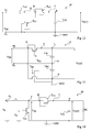
- the figure 1 schematically represents a single-phase rectifier circuit with a capacitor filter.
- the circuit 10 comprises two input terminals N 1 and N 2 between which is applied an oscillating voltage V IN , for example an alternating voltage.
- the AC voltage V IN is a sinusoidal voltage.
- the voltage V IN can be provided from a radiofrequency signal picked up by an antenna.
- the AC voltage V IN is a periodic voltage, comprising, for each period, a positive half cycle and a negative half cycle.
- the input terminal N 2 is connected to a source of a reference potential, for example the ground GND.
- the circuit 10 comprises a diode diode whose anode is connected to the input terminal N 1 and whose cathode is connected to a node E.
- a capacitor C is arranged between the node E and a node F connected to the ground GND .
- a resistor R is arranged in parallel across the capacitor C.
- the reference V OUT denotes the voltage between the nodes E and F.
- the function performed by the diode diode of the circuit 10 is performed by a diode-mounted MOS transistor.
- the figure 2 represents an example of a conventional structure of a diode-mounted MOS transistor M formed at a layer 12 of a semiconductor material, for example P-type doped monocrystalline silicon, having an upper surface 13.
- the transistor M is an N-channel transistor.
- the MOS transistor comprises an insulating portion 14, for example made of silicon oxide, covering the layer 12.
- Regions N-type dopants 18, 20 are provided in the layer 12 on either side of the insulating portion 14.
- the regions 18 and 20 extend optionally partially under the insulating portion 14.
- a P-type doped region 22 extends in the layer 12 from the surface 13.
- the region 22 is more heavily doped than the layer 12.
- the insulating portion 14 constitutes the gate insulator of the transistor M and the portion 16 constitutes the gate of the transistor M.
- the region 18 constitutes the source region of the transistor M and the region 20 constitutes the drain region of the transistor M.
- the connections of the elements of the transistor M are made by conductive tracks and vias not shown in detail.
- a terminal G connected to the portion 16, a terminal S connected to the source region 18 and a terminal D connected to the drain region.
- a terminal B is connected to the region 22 and makes it possible to polarize the layer 12.
- gate 16 of transistor M is indifferently referred to as the portion 16 or terminal G
- source of transistor M is region 18 or terminal S
- drain of the transistor M the region 20 or the terminal D.
- the transistor M being diode-mounted, the gate G is connected to the drain D.
- a first parasitic diode Diode BS corresponds to the junction between the layer 12 and the source region 18.
- a second parasitic diode Diode BD corresponds to the junction between the layer 12 and the region of drain 20.
- the figure 3 represents a rectifying circuit 25 similar to the circuit 10 of the figure 1 wherein the function filled by the diode diode is made from the diode-mounted transistor M of the figure 2 .
- the drain D of the transistor M is connected to the input terminal N 1 .
- the source S of the transistor M is connected to the node E.
- the substrate B of the transistor M is biased to ground GND.
- V DS is the voltage between the drain D and the source S of the transistor M
- V GS the voltage between the gate G and the source S of the transistor M
- I N1 is the current at the input terminal N 1 .
- the rectifier circuit 25 is intended to be connected to other circuits at the nodes E and F.
- the losses of the circuit 25 due to the conduction of the transistor M are proportional to the product of the voltage V DS , equal to the voltage V GS , and the current I DS . These losses occur, in steady state, when the voltage V GS is greater than the threshold voltage V t0 .
- the threshold voltage V t0 of the transistor M it is desirable for the threshold voltage V t0 of the transistor M to be as low as possible.
- the relation (1) shows that the threshold voltage V t0 is directly imposed by the value of the voltage V OUT which is generally fixed by the intended application of the rectifier circuit 25. It is therefore difficult to reduce the threshold voltage V t0 .
- the transistor M has a leakage current in the off state, in particular during the negative half-waves of the voltage V IN , which increases the losses of the circuit 25.
- the higher the threshold voltage of a MOS transistor is low the higher the leakage current is important. It is therefore not possible with the circuit 25 to simultaneously reduce the threshold voltage V t0 and the leakage current of the MOS transistor.
- the figure 4 represents the rectifier circuit 25 of the figure 3 in which the parasitic diode diodes BS and diode BD of the transistor M have been represented.
- the parasitic diode Diode BD extends between the terminals N 1 and N 2 , the anode of the diode Diode BD being connected to the input terminal N 2 .
- the parasitic diode Diode BS extends between the nodes E and F, the anode of the diode Diode BS being connected to the node F.
- the diode diode BD diode can become busy. This increases the losses of the circuit 25.
- the input impedance of the circuit 25 is high.
- the input impedance of the circuit 25 drops, which can be detrimental for certain applications. It may therefore be necessary to limit the amplitude of the voltage V IN to prevent the fall of the input impedance of the circuit 25.
- the figure 5 represents the structure of a diode-connected transistor M 'according to an exemplary embodiment of the invention.
- the transistor M ' comprises a substrate isolation structure 30 which delimits a portion 32 of the semiconductor layer 12 around the source and drain regions 18, 20 of the transistor M'.
- the portion 32, electrically isolated from the remainder of the layer 12, is called substrate 32 (in English bulk or body) of the transistor M 'in the following description.
- the doping of the region 32 is chosen to be sufficiently small so that the threshold voltage of the MOS transistor is substantially less than 0.6 V, preferably between 0.1 and 0.3 V.
- the substrate isolation structure 30 comprises a buried N type buried region 34 lying in the layer 12 and extending under the regions 18, 20 and 22.
- the substrate isolation structure 30 further comprises a side wall 36 corresponding to a region of the type N extending from the surface 13 of the layer 12 to the buried region 34 and surrounding the regions 18, 20 and 22.
- a region 38, N-type, more strongly doped than the region 36 extends in the region 36.
- An AC bias terminal of the substrate isolation structure 30 is connected to the region 38.
- a P-type doped region 39 extends in the layer 12 from the surface 13 outside the the substrate isolation structure.
- a terminal W is connected to the region 39 and makes it possible to polarize the remainder of the layer 12. Since the transistor M 'is diode-mounted, the gate G is connected to the In addition, the bias terminal B of the substrate 32 is connected to the drain D and the bias AC terminal of the substrate isolation structure 30 is connected to the source S.
- the polarization terminal W of the layer 12 is connected to the source of the reference potential GND.
- the intrinsic parasitic diodes of the transistor M ' corresponds to the junction between the substrate 32 of the transistor M 'and the source region 18.
- the diode Diode BD corresponds to the junction between the substrate 32 of the transistor M' and the drain region 20.
- the diode W diode corresponds to the junction between the substrate isolation structure 30 and the portion of the layer 12 outside the substrate isolation structure 30.
- the diode ISO diode corresponds to the junction between the substrate 32 of the transistor M 'and the substrate isolation structure 30.
- the figure 6 represents a rectifier circuit 40 similar to the rectifier circuit 25 of the figure 3 in which the transistor M 'is used.
- the diodes Diode ISO and Diode BS extend between the drain D and the node E, the anodes of the diodes Diode ISO and Diode BS being connected to the drain D.
- the diode Diode W extends between the nodes E and F, the anode of the diode diode W being connected to the node F.
- the substrate B being connected to the drain D of the transistor M ', the junction between the substrate 32 and the drain region 20 is short-circuited so that the diode diode BS does not intervene.
- the threshold voltage V t1 therefore varies as a function of the voltage V GS , that is to say as a function of the voltage V DS .
- V t1 decreases when the voltage V GS is positive and increases.
- the threshold voltage V t1 for which the transistor M ' turns on during a positive half cycle of the voltage V IN is lower than the threshold voltage V t0 defined by the relation (1).
- This threshold voltage of the MOS transistor is in any case significantly lower than the direct conduction voltage of a bipolar diode (about 0.6 V).
- the figure 7 represents curves 41, 42 of evolution of the current I DS as a function of the voltage V DS .
- Curve 41 corresponds to circuit 25 of the figure 4 for V OUT equal to 1 V and the curve 42 corresponds to the circuit 40 of the figure 6 .
- the threshold voltage V t1 of the transistor M ' according to the present embodiment of the invention being lower than the threshold voltage V t0 of the transistor M, for the same current I DS , the voltage V DS of the circuit of the figure 6 is less than that of the circuit of the figure 4 .
- the conduction losses of the circuit 40 are thus reduced with respect to the circuit 25.
- the figure 8 represents evolution curves 44, 46 of the leakage current respectively of the transistors M and M 'during a negative alternation of the voltage V IN .
- the threshold voltage V t0 of the transistor M does not vary substantially during a negative half-wave of the voltage V IN (relation (1)). Throughout the negative half cycle, the voltage V GS is negative and greater, in absolute value, than V OUT . The voltage V t1 is therefore greater than the threshold voltage V t0 throughout the negative half cycle. As the leakage current of a MOS transistor decreases as the threshold voltage of the transistor increases, the leakage current of the transistor M 'is smaller than the leakage current of the transistor M by at least a factor of 2 over most of the transistor. negative alternation.
- the figure 9 represents curves 48, 50 of evolution of the current I N1 to the input terminal N 1 as a function of the voltage V IN during a negative half-wave of the voltage V IN .
- Curve 48 corresponds to circuit 25 of figure 4 and the curve 50 corresponds to circuit 40 of the figure 6 .
- the curve 48 comprises a first part 51 which is strongly increasing followed by a second part 52 which is very slightly increasing.
- Curve 50 comprises only a very weakly increasing part.
- the parasitic diode Diode BD tends to be conducting which results in a negative current I N1 which increases strongly, in absolute value, when the negative voltage V IN increases, as a value. absolute (part 51 of curve 48).
- the current I N1 corresponds to the leakage current of the transistor M during the negative half cycle (part 52 of the curve 48).
- the circuit 40 there is no parasitic diode between the input terminals N 1 and N 2 .
- the curve 50 reflects the fact that the current I D is only equal to the leakage current of the transistor M 'throughout the negative half cycle which is lower than the leakage current of the transistor M. The additional losses during an alternation negative of the voltage V IN are therefore reduced for the circuit 40 with respect to the circuit 25.
- the figure 10 represents another example of a diode-mounted MOS transistor structure M "according to the invention, the structure of the transistor M" is similar to that of the transistor M 'of the figure 5 with the difference that the terminal CA is connected to the drain D and not to the source S.
- the terminal W is, as for the transistor M ', connected to the ground GND.
- the expression of the threshold voltage of the transistor M " is given by the relation (2): The same advantages as for the reduction of the threshold voltage are found as for the embodiment described above in relation to the figure 5 .
- the figure 11 represents a circuit 55 similar to the circuit 40 of the figure 6 With the difference that the transistor M 'is replaced by the transistor M ", the parasitic diode Diode W is then situated between the input terminals N 1 and N 2, and the disadvantages of the circuit 10 of the figure 4 with losses due to the conduction of the diode diode W diode during negative halfwaves of the voltage V 1N .
- MOS transistor M ' according to the present embodiment of the invention has been described for a rectifier circuit 40, the transistor M' or M "may be used for other types of electronic circuits implementing a MOS transistor. diode mounted whose drain receives an oscillating signal.
- FIGS 12 to 14 represent other examples of electronic circuits in which the MOS transistor M 'or M "according to the embodiments of the invention described above can be used.
- the figure 12 represents an example of a charge pump energy recovery circuit 60.
- the circuit 60 comprises input terminals A 1 and A 2 receiving the AC voltage V 1N .
- Terminal A 2 is connected to ground GND.
- the terminal A 1 is connected to an armature of a capacitor C A1 whose other armature is connected to a node H.
- a diode-connected transistor T A1 is provided between the node H and the input terminal A 2 .
- the substrate, the gate and the source of transistor T A1 are connected to ground GND.
- the transistor T A1 may have the structure of the transistor M of the figure 2 .
- a diode-connected transistor T A2 is arranged between the node H and a node K.
- the transistor T A2 corresponds to the transistor M 'or M "according to the embodiments of the invention described above.
- the drain of the transistor T A2 are connected to the node H.
- the terminal CA, not shown, and the source of the transistor T A1 are connected to the node K.
- a capacitor C A2 is provided between the node K and the ground GND. OUT is the voltage between node K and ground GND.
- the figure 13 represents an example of a differential input energy recovery circuit 62.
- the circuit 62 comprises input terminals B 1 and B 2 receiving the AC voltage V 1N .
- a diode-connected transistor T B1 is provided between the input terminal B 2 and a node L.
- the transistor T B1 corresponds to the transistor M 'or M "according to the embodiments of the invention described above.
- gate and the drain of the transistor T B1 are connected to the terminal B 1.
- the terminal CA, not shown, and the source of the transistor T A1 are connected to the node L.
- a capacitor C B1 is arranged between the node L and a node O connected to the input terminal B 2.
- a capacitor C B2 is disposed between the node O and a node N.
- the node N is connected to the ground GND
- a diode-connected transistor T B2 is provided between the input terminal B 1 and the node N.
- the substrate, the gate and the drain of the transistor T B2 are connected to the ground GND
- the transistor T B2 can have the structure of the transistor M of the figure 2 .
- the voltage V OUT is taken between the nodes L and N.
- the figure 14 represents an example of an elevator chopper circuit 64.
- the circuit 64 comprises an input terminal E 1 receiving a voltage V E , for example a DC voltage.
- the terminal E 1 is connected to a node P by an inductance L.
- a transistor T C1 is provided between the node P and the ground GND.
- the gate of transistor T C1 receives a succession of voltage pulses V C whose frequency depends on the desired voltage V OUT .
- the oscillating voltage V 1N is the voltage between the node P and the ground GND.
- a diode-connected transistor T C2 is disposed between the node P and a node Q.
- the transistor T C2 corresponds to the transistor M 'or M "according to the embodiments of the invention described above.
- the drain of the transistor T C2 are connected to the node P.
- the terminal CA, not shown, and the source of the transistor T C2 are connected to the node Q.
- a capacitor C1 is arranged between the node Q and the ground GND. is provided across the capacitor C C1.
- the voltage V OUT corresponds to the voltage across the capacitor C C1.
- the operation of the circuit 64 during a cycle of control of transistor T C1 is schematically the following.
- the transistor T C1 When the transistor T C1 is conducting, the voltage V IN is substantially zero.
- Transistor T C2 is then blocked. At the moment when the transistor T C1 goes from the on state to the off state, the voltage V IN rises sharply temporarily due to the inductance L.
- the transistor T C2 becomes conducting resulting in the charge of the capacitor C
- the voltage V IN then decreases to V E causing the blocking of the transistor T C2 .
- the present invention also applies to a P-channel MOS transistor.
- the MOS transistor is, for example, made in a box.
- type N provided at a p-type doped layer.
- the N-type well forms the substrate of the transistor.
- P-type doped regions are provided in the N-type well and form the source and drain regions of the MOS transistor.
- the gate and the substrate are connected to the drain of the transistor.
Landscapes
- Engineering & Computer Science (AREA)
- Power Engineering (AREA)
- Metal-Oxide And Bipolar Metal-Oxide Semiconductor Integrated Circuits (AREA)
- Semiconductor Integrated Circuits (AREA)
Applications Claiming Priority (1)
| Application Number | Priority Date | Filing Date | Title |
|---|---|---|---|
| FR0854555 | 2008-07-04 |
Publications (2)
| Publication Number | Publication Date |
|---|---|
| EP2141741A2 true EP2141741A2 (de) | 2010-01-06 |
| EP2141741A3 EP2141741A3 (de) | 2012-08-15 |
Family
ID=40263168
Family Applications (1)
| Application Number | Title | Priority Date | Filing Date |
|---|---|---|---|
| EP09164596A Withdrawn EP2141741A3 (de) | 2008-07-04 | 2009-07-03 | Elektronischer Schaltkreis mit einem MOS-Transistor in Diodenschaltung mit verbessertem Wirkungsgrad |
Country Status (2)
| Country | Link |
|---|---|
| US (1) | US8445947B2 (de) |
| EP (1) | EP2141741A3 (de) |
Cited By (1)
| Publication number | Priority date | Publication date | Assignee | Title |
|---|---|---|---|---|
| FR3041838A1 (fr) * | 2015-09-28 | 2017-03-31 | Commissariat Energie Atomique | Circuit electronique elementaire pour etage d'amplification ou de recopie de signaux analogiques |
Families Citing this family (8)
| Publication number | Priority date | Publication date | Assignee | Title |
|---|---|---|---|---|
| WO2010080855A2 (en) | 2009-01-06 | 2010-07-15 | Lakota Technologies Inc. | Self-bootstrapping field effect diode structures and methods |
| JP2011138214A (ja) * | 2009-12-25 | 2011-07-14 | Toshiba Corp | 半導体集積回路装置 |
| WO2011108374A1 (en) * | 2010-03-05 | 2011-09-09 | Semiconductor Energy Laboratory Co., Ltd. | Semiconductor device and method for manufacturing semiconductor device |
| JP5587135B2 (ja) * | 2010-10-28 | 2014-09-10 | ルネサスエレクトロニクス株式会社 | 無線通信用半導体装置 |
| DE102010062677A1 (de) * | 2010-12-09 | 2012-06-14 | Robert Bosch Gmbh | Generatorvorrichtung zur Spannungsversorgung eines Kraftfahrzeugs |
| US9553087B1 (en) * | 2015-11-02 | 2017-01-24 | Taiwan Semiconductor Manufacturing Company Ltd. | Semiconductor device |
| US20200194459A1 (en) * | 2018-12-18 | 2020-06-18 | Vanguard International Semiconductor Corporation | Semiconductor devices and methods for fabricating the same |
| CN112421969A (zh) * | 2020-06-22 | 2021-02-26 | 杭州炬华科技股份有限公司 | 一种增强型阻容电源电路 |
Family Cites Families (30)
| Publication number | Priority date | Publication date | Assignee | Title |
|---|---|---|---|---|
| US5240865A (en) * | 1990-07-30 | 1993-08-31 | Texas Instruments Incorporated | Method of forming a thyristor on an SOI substrate |
| JP2771729B2 (ja) * | 1992-04-16 | 1998-07-02 | 三菱電機株式会社 | チャージポンプ回路 |
| US5801420A (en) * | 1994-09-08 | 1998-09-01 | Fuji Electric Co. Ltd. | Lateral semiconductor arrangement for power ICS |
| US6285240B1 (en) * | 1999-01-14 | 2001-09-04 | Macronix International Co., Ltd. | Low threshold MOS two phase negative charge pump |
| TW419806B (en) * | 1999-01-25 | 2001-01-21 | Winbond Electronics Corp | Electrostatic discharge device for circuit with an operating voltage larger than the supplied voltage |
| JP4617527B2 (ja) * | 1999-04-08 | 2011-01-26 | 株式会社デンソー | 回路装置 |
| TW451423B (en) * | 2000-02-01 | 2001-08-21 | Ind Tech Res Inst | Latch-up structure for improving CMOS processing using latch-up ion implantation and the manufacturing method thereof |
| US6492208B1 (en) * | 2000-09-28 | 2002-12-10 | Taiwan Semiconductor Manufacturing Company | Embedded SCR protection device for output and input pad |
| US6455902B1 (en) * | 2000-12-06 | 2002-09-24 | International Business Machines Corporation | BiCMOS ESD circuit with subcollector/trench-isolated body mosfet for mixed signal analog/digital RF applications |
| US6537921B2 (en) * | 2001-05-23 | 2003-03-25 | Vram Technologies, Llc | Vertical metal oxide silicon field effect semiconductor diodes |
| JP4124981B2 (ja) * | 2001-06-04 | 2008-07-23 | 株式会社ルネサステクノロジ | 電力用半導体装置および電源回路 |
| US6900091B2 (en) * | 2002-08-14 | 2005-05-31 | Advanced Analogic Technologies, Inc. | Isolated complementary MOS devices in epi-less substrate |
| US6934171B2 (en) * | 2003-09-26 | 2005-08-23 | Lsi Logic Corporation | Semiconductor integrated circuit having voltage-down circuit regulator and charge sharing |
| WO2005057628A2 (en) * | 2003-12-08 | 2005-06-23 | University Of South Florida | A method and apparatus for reducing leakage in integrated circuits |
| FR2864343A1 (fr) * | 2003-12-19 | 2005-06-24 | St Microelectronics Sa | Triac fonctionnant dans les quadrants q1 et q4 |
| US7304354B2 (en) * | 2004-02-17 | 2007-12-04 | Silicon Space Technology Corp. | Buried guard ring and radiation hardened isolation structures and fabrication methods |
| JP4593126B2 (ja) * | 2004-02-18 | 2010-12-08 | 三菱電機株式会社 | 半導体装置 |
| US7127216B2 (en) * | 2004-07-06 | 2006-10-24 | Avago Technologies Wireless Ip (Singapore) Pte. Ltd. | Integrated circuit and method for receiving and transmitting signals of different frequency bands |
| JP4566692B2 (ja) * | 2004-10-28 | 2010-10-20 | シャープ株式会社 | 発光ダイオード駆動装置及びそれを備えた光伝送装置 |
| JP4703196B2 (ja) * | 2005-01-18 | 2011-06-15 | 株式会社東芝 | 半導体装置 |
| WO2006087822A1 (ja) | 2005-02-16 | 2006-08-24 | Hitachi, Ltd. | 電子タグチップ |
| US7500118B2 (en) * | 2005-03-28 | 2009-03-03 | Akros Silicon Inc. | Network device with power potential rectifier |
| KR100724563B1 (ko) * | 2005-04-29 | 2007-06-04 | 삼성전자주식회사 | 다중 일함수 금속 질화물 게이트 전극을 갖는 모스트랜지스터들, 이를 채택하는 씨모스 집적회로 소자들 및그 제조방법들 |
| US7317229B2 (en) * | 2005-07-20 | 2008-01-08 | Applied Materials, Inc. | Gate electrode structures and methods of manufacture |
| KR100639231B1 (ko) * | 2005-12-30 | 2006-11-01 | 주식회사 하이닉스반도체 | 정전기 방전 보호 회로 |
| JP2007220755A (ja) * | 2006-02-14 | 2007-08-30 | Toshiba Corp | 半導体装置及びその製造方法 |
| US20070228425A1 (en) * | 2006-04-04 | 2007-10-04 | Miller Gayle W | Method and manufacturing low leakage MOSFETs and FinFETs |
| EP1944801A1 (de) * | 2007-01-10 | 2008-07-16 | Interuniversitair Microelektronica Centrum | Verfahren zur Herstellung einer CMOS-Vorrichtung mit dualer Austrittsarbeit |
| JP4989309B2 (ja) * | 2007-05-18 | 2012-08-01 | 株式会社半導体エネルギー研究所 | 液晶表示装置 |
| US7745292B2 (en) * | 2007-10-15 | 2010-06-29 | Infineon Technologies Ag | Method for fabricating a semiconductor gate structure |
-
2009
- 2009-07-02 US US12/497,210 patent/US8445947B2/en active Active
- 2009-07-03 EP EP09164596A patent/EP2141741A3/de not_active Withdrawn
Cited By (3)
| Publication number | Priority date | Publication date | Assignee | Title |
|---|---|---|---|---|
| FR3041838A1 (fr) * | 2015-09-28 | 2017-03-31 | Commissariat Energie Atomique | Circuit electronique elementaire pour etage d'amplification ou de recopie de signaux analogiques |
| WO2017055709A1 (fr) * | 2015-09-28 | 2017-04-06 | Commissariat A L'energie Atomique Et Aux Energies Alternatives | Circuit electronique elementaire pour etage d'amplification ou de recopie de signaux analogiques |
| US10644690B2 (en) | 2015-09-28 | 2020-05-05 | Commissariat à l'énergie atomique et aux énergies alternatives | Elementary electronic circuit for stage of amplification or repeat of analog signals |
Also Published As
| Publication number | Publication date |
|---|---|
| EP2141741A3 (de) | 2012-08-15 |
| US20100034000A1 (en) | 2010-02-11 |
| US8445947B2 (en) | 2013-05-21 |
Similar Documents
| Publication | Publication Date | Title |
|---|---|---|
| EP2141741A2 (de) | Elektronischer Schaltkreis mit einem MOS-Transistor in Diodenschaltung mit verbessertem Wirkungsgrad | |
| FR2615656A1 (fr) | Dispositif semi-conducteur monolithique integre a conduction bidirectionnelle et procede de fabrication | |
| FR2987496A1 (fr) | Circuit de protection contre les decharges electrostatiques | |
| WO1998024172A2 (fr) | Dispositif de redressement de tension a composants integres | |
| FR3033938A1 (fr) | Diode zener a tension de claquage ajustable | |
| FR2858493A1 (fr) | Circuit d'attaque a autoelevation | |
| FR2993401A1 (fr) | Transistor mos sur soi protege contre des surtensions | |
| EP4456362A1 (de) | Überspannungsschutzschaltung | |
| EP2913849A1 (de) | Elektronische Vorrichtung mit in Gegenrichtung vorgespanntem HEMT-Transistor | |
| FR2477338A1 (fr) | Circuit de sortie empeche de se bloquer du fait d'impulsions de tension produites par une charge inductive | |
| FR3106941A1 (fr) | Protection contre des surtensions | |
| EP2966687B1 (de) | Cmos-bilderfassungssensor | |
| EP0881682B1 (de) | Hochspannungsschutzanordnung für einen integrierten MOS-Leistungstransistor | |
| FR2737065A1 (fr) | Dispositif semiconducteur incluant un amplificateur de puissance et appareil de telecommunication mobile incluant un tel dispositif semiconducteur | |
| EP4102701A1 (de) | Leistungswandler | |
| FR3131981A1 (fr) | Dispositif de protection contre les décharges électrostatiques | |
| EP3032729A1 (de) | Gleichstrom-gleichstrom-wandler mit kaltstart | |
| EP0128062A1 (de) | Feldeffekttransistor vom Anreicherungs-Typ | |
| EP4086973A1 (de) | Unidirektionale vorrichtung zur unterdrückung von transienten spannungen ohne direktleitung | |
| EP0635886B1 (de) | Monolitisches Bauelement mit einer Schutzdiode, die mit einer Vielzahl von seriell geschalteten Diodenpaaren parallelgeschaltet ist, und dessen Verwendungen | |
| EP4344065A1 (de) | Transistorsteuerschaltung | |
| EP0820135B1 (de) | Statischer selbsthaltender Mikroschalter | |
| FR3011121A1 (fr) | Assemblage de puces de circuits integres comprenant un composant de protection contre les surtensions | |
| FR3033937A1 (fr) | Diode zener a faible tension de claquage ajustable | |
| EP0800131B1 (de) | Integrierte Stromquellenschaltung |
Legal Events
| Date | Code | Title | Description |
|---|---|---|---|
| PUAI | Public reference made under article 153(3) epc to a published international application that has entered the european phase |
Free format text: ORIGINAL CODE: 0009012 |
|
| AK | Designated contracting states |
Kind code of ref document: A2 Designated state(s): AT BE BG CH CY CZ DE DK EE ES FI FR GB GR HR HU IE IS IT LI LT LU LV MC MK MT NL NO PL PT RO SE SI SK SM TR |
|
| PUAL | Search report despatched |
Free format text: ORIGINAL CODE: 0009013 |
|
| AK | Designated contracting states |
Kind code of ref document: A3 Designated state(s): AT BE BG CH CY CZ DE DK EE ES FI FR GB GR HR HU IE IS IT LI LT LU LV MC MK MT NL NO PL PT RO SE SI SK SM TR |
|
| AX | Request for extension of the european patent |
Extension state: AL BA RS |
|
| RIC1 | Information provided on ipc code assigned before grant |
Ipc: H01L 27/08 20060101AFI20120710BHEP Ipc: H01L 21/761 20060101ALI20120710BHEP Ipc: H01L 29/78 20060101ALI20120710BHEP Ipc: H02M 7/217 20060101ALI20120710BHEP Ipc: H02M 3/07 20060101ALI20120710BHEP Ipc: H01L 29/861 20060101ALI20120710BHEP |
|
| 17P | Request for examination filed |
Effective date: 20121220 |
|
| 17Q | First examination report despatched |
Effective date: 20130205 |
|
| STAA | Information on the status of an ep patent application or granted ep patent |
Free format text: STATUS: THE APPLICATION HAS BEEN WITHDRAWN |
|
| 18W | Application withdrawn |
Effective date: 20150529 |