EP2144109B1 - Ecran à cristaux liquides et procédé de fabrication d'un écran à cristaux liquides - Google Patents
Ecran à cristaux liquides et procédé de fabrication d'un écran à cristaux liquides Download PDFInfo
- Publication number
- EP2144109B1 EP2144109B1 EP07860369A EP07860369A EP2144109B1 EP 2144109 B1 EP2144109 B1 EP 2144109B1 EP 07860369 A EP07860369 A EP 07860369A EP 07860369 A EP07860369 A EP 07860369A EP 2144109 B1 EP2144109 B1 EP 2144109B1
- Authority
- EP
- European Patent Office
- Prior art keywords
- electrode
- liquid crystal
- layer
- crystal display
- display device
- Prior art date
- Legal status (The legal status is an assumption and is not a legal conclusion. Google has not performed a legal analysis and makes no representation as to the accuracy of the status listed.)
- Not-in-force
Links
- 239000004973 liquid crystal related substance Substances 0.000 title claims abstract description 150
- 238000004519 manufacturing process Methods 0.000 title claims abstract description 70
- 239000000758 substrate Substances 0.000 claims abstract description 178
- 229910052751 metal Inorganic materials 0.000 claims abstract description 132
- 239000002184 metal Substances 0.000 claims abstract description 132
- 239000000463 material Substances 0.000 claims abstract description 21
- 239000004065 semiconductor Substances 0.000 claims description 79
- 239000010410 layer Substances 0.000 description 341
- 239000010408 film Substances 0.000 description 69
- 238000000034 method Methods 0.000 description 59
- 239000011229 interlayer Substances 0.000 description 35
- 238000000206 photolithography Methods 0.000 description 34
- 238000010276 construction Methods 0.000 description 27
- 238000004544 sputter deposition Methods 0.000 description 22
- 238000010586 diagram Methods 0.000 description 14
- 230000005540 biological transmission Effects 0.000 description 12
- 239000011347 resin Substances 0.000 description 10
- 229920005989 resin Polymers 0.000 description 10
- 229910021417 amorphous silicon Inorganic materials 0.000 description 8
- 239000004925 Acrylic resin Substances 0.000 description 7
- 229920000178 Acrylic resin Polymers 0.000 description 7
- 239000000470 constituent Substances 0.000 description 7
- 230000000694 effects Effects 0.000 description 7
- 238000004528 spin coating Methods 0.000 description 7
- 229910052715 tantalum Inorganic materials 0.000 description 7
- GUVRBAGPIYLISA-UHFFFAOYSA-N tantalum atom Chemical compound [Ta] GUVRBAGPIYLISA-UHFFFAOYSA-N 0.000 description 7
- VYPSYNLAJGMNEJ-UHFFFAOYSA-N Silicium dioxide Chemical compound O=[Si]=O VYPSYNLAJGMNEJ-UHFFFAOYSA-N 0.000 description 5
- 239000011159 matrix material Substances 0.000 description 4
- 238000007493 shaping process Methods 0.000 description 4
- 230000005684 electric field Effects 0.000 description 3
- 238000005530 etching Methods 0.000 description 3
- OAICVXFJPJFONN-UHFFFAOYSA-N Phosphorus Chemical compound [P] OAICVXFJPJFONN-UHFFFAOYSA-N 0.000 description 2
- 229910052581 Si3N4 Inorganic materials 0.000 description 2
- 239000011651 chromium Substances 0.000 description 2
- 229910052681 coesite Inorganic materials 0.000 description 2
- 229910052906 cristobalite Inorganic materials 0.000 description 2
- 238000001312 dry etching Methods 0.000 description 2
- 229910052698 phosphorus Inorganic materials 0.000 description 2
- 239000011574 phosphorus Substances 0.000 description 2
- 239000000377 silicon dioxide Substances 0.000 description 2
- HQVNEWCFYHHQES-UHFFFAOYSA-N silicon nitride Chemical compound N12[Si]34N5[Si]62N3[Si]51N64 HQVNEWCFYHHQES-UHFFFAOYSA-N 0.000 description 2
- 229910052682 stishovite Inorganic materials 0.000 description 2
- 239000010409 thin film Substances 0.000 description 2
- 239000010936 titanium Substances 0.000 description 2
- 229910052905 tridymite Inorganic materials 0.000 description 2
- 238000001039 wet etching Methods 0.000 description 2
- VYZAMTAEIAYCRO-UHFFFAOYSA-N Chromium Chemical compound [Cr] VYZAMTAEIAYCRO-UHFFFAOYSA-N 0.000 description 1
- ZOKXTWBITQBERF-UHFFFAOYSA-N Molybdenum Chemical compound [Mo] ZOKXTWBITQBERF-UHFFFAOYSA-N 0.000 description 1
- 229910004205 SiNX Inorganic materials 0.000 description 1
- BLRPTPMANUNPDV-UHFFFAOYSA-N Silane Chemical compound [SiH4] BLRPTPMANUNPDV-UHFFFAOYSA-N 0.000 description 1
- RTAQQCXQSZGOHL-UHFFFAOYSA-N Titanium Chemical compound [Ti] RTAQQCXQSZGOHL-UHFFFAOYSA-N 0.000 description 1
- 239000000956 alloy Substances 0.000 description 1
- 229910045601 alloy Inorganic materials 0.000 description 1
- 229910052782 aluminium Inorganic materials 0.000 description 1
- XAGFODPZIPBFFR-UHFFFAOYSA-N aluminium Chemical compound [Al] XAGFODPZIPBFFR-UHFFFAOYSA-N 0.000 description 1
- PNEYBMLMFCGWSK-UHFFFAOYSA-N aluminium oxide Inorganic materials [O-2].[O-2].[O-2].[Al+3].[Al+3] PNEYBMLMFCGWSK-UHFFFAOYSA-N 0.000 description 1
- 230000015572 biosynthetic process Effects 0.000 description 1
- 239000003990 capacitor Substances 0.000 description 1
- 229910052804 chromium Inorganic materials 0.000 description 1
- 229910052593 corundum Inorganic materials 0.000 description 1
- 239000008246 gaseous mixture Substances 0.000 description 1
- 239000011521 glass Substances 0.000 description 1
- 229910052750 molybdenum Inorganic materials 0.000 description 1
- 239000011733 molybdenum Substances 0.000 description 1
- 150000004767 nitrides Chemical class 0.000 description 1
- 230000003287 optical effect Effects 0.000 description 1
- 239000012788 optical film Substances 0.000 description 1
- TWNQGVIAIRXVLR-UHFFFAOYSA-N oxo(oxoalumanyloxy)alumane Chemical compound O=[Al]O[Al]=O TWNQGVIAIRXVLR-UHFFFAOYSA-N 0.000 description 1
- BPUBBGLMJRNUCC-UHFFFAOYSA-N oxygen(2-);tantalum(5+) Chemical compound [O-2].[O-2].[O-2].[O-2].[O-2].[Ta+5].[Ta+5] BPUBBGLMJRNUCC-UHFFFAOYSA-N 0.000 description 1
- 229910052814 silicon oxide Inorganic materials 0.000 description 1
- 229910001936 tantalum oxide Inorganic materials 0.000 description 1
- PBCFLUZVCVVTBY-UHFFFAOYSA-N tantalum pentoxide Inorganic materials O=[Ta](=O)O[Ta](=O)=O PBCFLUZVCVVTBY-UHFFFAOYSA-N 0.000 description 1
- 229910052719 titanium Inorganic materials 0.000 description 1
- WFKWXMTUELFFGS-UHFFFAOYSA-N tungsten Chemical compound [W] WFKWXMTUELFFGS-UHFFFAOYSA-N 0.000 description 1
- 229910052721 tungsten Inorganic materials 0.000 description 1
- 239000010937 tungsten Substances 0.000 description 1
- 229910001845 yogo sapphire Inorganic materials 0.000 description 1
Images


Classifications
-
- G—PHYSICS
- G02—OPTICS
- G02F—OPTICAL DEVICES OR ARRANGEMENTS FOR THE CONTROL OF LIGHT BY MODIFICATION OF THE OPTICAL PROPERTIES OF THE MEDIA OF THE ELEMENTS INVOLVED THEREIN; NON-LINEAR OPTICS; FREQUENCY-CHANGING OF LIGHT; OPTICAL LOGIC ELEMENTS; OPTICAL ANALOGUE/DIGITAL CONVERTERS
- G02F1/00—Devices or arrangements for the control of the intensity, colour, phase, polarisation or direction of light arriving from an independent light source, e.g. switching, gating or modulating; Non-linear optics
- G02F1/01—Devices or arrangements for the control of the intensity, colour, phase, polarisation or direction of light arriving from an independent light source, e.g. switching, gating or modulating; Non-linear optics for the control of the intensity, phase, polarisation or colour
- G02F1/13—Devices or arrangements for the control of the intensity, colour, phase, polarisation or direction of light arriving from an independent light source, e.g. switching, gating or modulating; Non-linear optics for the control of the intensity, phase, polarisation or colour based on liquid crystals, e.g. single liquid crystal display cells
- G02F1/133—Constructional arrangements; Operation of liquid crystal cells; Circuit arrangements
- G02F1/1333—Constructional arrangements; Manufacturing methods
- G02F1/1335—Structural association of cells with optical devices, e.g. polarisers or reflectors
- G02F1/133553—Reflecting elements
- G02F1/133555—Transflectors
-
- G—PHYSICS
- G02—OPTICS
- G02F—OPTICAL DEVICES OR ARRANGEMENTS FOR THE CONTROL OF LIGHT BY MODIFICATION OF THE OPTICAL PROPERTIES OF THE MEDIA OF THE ELEMENTS INVOLVED THEREIN; NON-LINEAR OPTICS; FREQUENCY-CHANGING OF LIGHT; OPTICAL LOGIC ELEMENTS; OPTICAL ANALOGUE/DIGITAL CONVERTERS
- G02F1/00—Devices or arrangements for the control of the intensity, colour, phase, polarisation or direction of light arriving from an independent light source, e.g. switching, gating or modulating; Non-linear optics
- G02F1/01—Devices or arrangements for the control of the intensity, colour, phase, polarisation or direction of light arriving from an independent light source, e.g. switching, gating or modulating; Non-linear optics for the control of the intensity, phase, polarisation or colour
- G02F1/13—Devices or arrangements for the control of the intensity, colour, phase, polarisation or direction of light arriving from an independent light source, e.g. switching, gating or modulating; Non-linear optics for the control of the intensity, phase, polarisation or colour based on liquid crystals, e.g. single liquid crystal display cells
- G02F1/133—Constructional arrangements; Operation of liquid crystal cells; Circuit arrangements
- G02F1/1333—Constructional arrangements; Manufacturing methods
- G02F1/1335—Structural association of cells with optical devices, e.g. polarisers or reflectors
- G02F1/133553—Reflecting elements
-
- G—PHYSICS
- G02—OPTICS
- G02F—OPTICAL DEVICES OR ARRANGEMENTS FOR THE CONTROL OF LIGHT BY MODIFICATION OF THE OPTICAL PROPERTIES OF THE MEDIA OF THE ELEMENTS INVOLVED THEREIN; NON-LINEAR OPTICS; FREQUENCY-CHANGING OF LIGHT; OPTICAL LOGIC ELEMENTS; OPTICAL ANALOGUE/DIGITAL CONVERTERS
- G02F1/00—Devices or arrangements for the control of the intensity, colour, phase, polarisation or direction of light arriving from an independent light source, e.g. switching, gating or modulating; Non-linear optics
- G02F1/01—Devices or arrangements for the control of the intensity, colour, phase, polarisation or direction of light arriving from an independent light source, e.g. switching, gating or modulating; Non-linear optics for the control of the intensity, phase, polarisation or colour
- G02F1/13—Devices or arrangements for the control of the intensity, colour, phase, polarisation or direction of light arriving from an independent light source, e.g. switching, gating or modulating; Non-linear optics for the control of the intensity, phase, polarisation or colour based on liquid crystals, e.g. single liquid crystal display cells
- G02F1/133—Constructional arrangements; Operation of liquid crystal cells; Circuit arrangements
- G02F1/1333—Constructional arrangements; Manufacturing methods
- G02F1/1343—Electrodes
- G02F1/134309—Electrodes characterised by their geometrical arrangement
- G02F1/134372—Electrodes characterised by their geometrical arrangement for fringe field switching [FFS] where the common electrode is not patterned
-
- G—PHYSICS
- G02—OPTICS
- G02F—OPTICAL DEVICES OR ARRANGEMENTS FOR THE CONTROL OF LIGHT BY MODIFICATION OF THE OPTICAL PROPERTIES OF THE MEDIA OF THE ELEMENTS INVOLVED THEREIN; NON-LINEAR OPTICS; FREQUENCY-CHANGING OF LIGHT; OPTICAL LOGIC ELEMENTS; OPTICAL ANALOGUE/DIGITAL CONVERTERS
- G02F1/00—Devices or arrangements for the control of the intensity, colour, phase, polarisation or direction of light arriving from an independent light source, e.g. switching, gating or modulating; Non-linear optics
- G02F1/01—Devices or arrangements for the control of the intensity, colour, phase, polarisation or direction of light arriving from an independent light source, e.g. switching, gating or modulating; Non-linear optics for the control of the intensity, phase, polarisation or colour
- G02F1/13—Devices or arrangements for the control of the intensity, colour, phase, polarisation or direction of light arriving from an independent light source, e.g. switching, gating or modulating; Non-linear optics for the control of the intensity, phase, polarisation or colour based on liquid crystals, e.g. single liquid crystal display cells
- G02F1/133—Constructional arrangements; Operation of liquid crystal cells; Circuit arrangements
- G02F1/136—Liquid crystal cells structurally associated with a semi-conducting layer or substrate, e.g. cells forming part of an integrated circuit
- G02F1/1362—Active matrix addressed cells
- G02F1/136227—Through-hole connection of the pixel electrode to the active element through an insulation layer
-
- G—PHYSICS
- G02—OPTICS
- G02F—OPTICAL DEVICES OR ARRANGEMENTS FOR THE CONTROL OF LIGHT BY MODIFICATION OF THE OPTICAL PROPERTIES OF THE MEDIA OF THE ELEMENTS INVOLVED THEREIN; NON-LINEAR OPTICS; FREQUENCY-CHANGING OF LIGHT; OPTICAL LOGIC ELEMENTS; OPTICAL ANALOGUE/DIGITAL CONVERTERS
- G02F1/00—Devices or arrangements for the control of the intensity, colour, phase, polarisation or direction of light arriving from an independent light source, e.g. switching, gating or modulating; Non-linear optics
- G02F1/01—Devices or arrangements for the control of the intensity, colour, phase, polarisation or direction of light arriving from an independent light source, e.g. switching, gating or modulating; Non-linear optics for the control of the intensity, phase, polarisation or colour
- G02F1/13—Devices or arrangements for the control of the intensity, colour, phase, polarisation or direction of light arriving from an independent light source, e.g. switching, gating or modulating; Non-linear optics for the control of the intensity, phase, polarisation or colour based on liquid crystals, e.g. single liquid crystal display cells
- G02F1/133—Constructional arrangements; Operation of liquid crystal cells; Circuit arrangements
- G02F1/136—Liquid crystal cells structurally associated with a semi-conducting layer or substrate, e.g. cells forming part of an integrated circuit
- G02F1/1362—Active matrix addressed cells
- G02F1/136231—Active matrix addressed cells for reducing the number of lithographic steps
- G02F1/136236—Active matrix addressed cells for reducing the number of lithographic steps using a grey or half tone lithographic process
-
- G—PHYSICS
- G02—OPTICS
- G02F—OPTICAL DEVICES OR ARRANGEMENTS FOR THE CONTROL OF LIGHT BY MODIFICATION OF THE OPTICAL PROPERTIES OF THE MEDIA OF THE ELEMENTS INVOLVED THEREIN; NON-LINEAR OPTICS; FREQUENCY-CHANGING OF LIGHT; OPTICAL LOGIC ELEMENTS; OPTICAL ANALOGUE/DIGITAL CONVERTERS
- G02F1/00—Devices or arrangements for the control of the intensity, colour, phase, polarisation or direction of light arriving from an independent light source, e.g. switching, gating or modulating; Non-linear optics
- G02F1/01—Devices or arrangements for the control of the intensity, colour, phase, polarisation or direction of light arriving from an independent light source, e.g. switching, gating or modulating; Non-linear optics for the control of the intensity, phase, polarisation or colour
- G02F1/13—Devices or arrangements for the control of the intensity, colour, phase, polarisation or direction of light arriving from an independent light source, e.g. switching, gating or modulating; Non-linear optics for the control of the intensity, phase, polarisation or colour based on liquid crystals, e.g. single liquid crystal display cells
- G02F1/133—Constructional arrangements; Operation of liquid crystal cells; Circuit arrangements
- G02F1/136—Liquid crystal cells structurally associated with a semi-conducting layer or substrate, e.g. cells forming part of an integrated circuit
- G02F1/1362—Active matrix addressed cells
- G02F1/136286—Wiring, e.g. gate line, drain line
Definitions
- the present invention relates to a reflection-type or transflective-type liquid crystal display device capable of performing display by utilizing reflected light.
- Liquid crystal display devices include: the TN (Twisted Nematic) mode liquid crystal display device, in which a pixel electrode (picture element electrode) is provided on one of a pair of substrates (an upper substrate and a lower substrate) between which a liquid crystal layer is interposed, and a counter electrode on the other, such that displaying is performed by controlling the orientation of liquid crystal within a plane which is perpendicular to the substrate plane in accordance with an electric field occurring between both electrodes; and the FFS (Fringe-Field Switching) mode liquid crystal display device and the IPS (In-Plane Switching) mode liquid crystal display device, in which a pixel electrode and a counter electrode (lower electrode) are provided on one of a pair of opposing substrates, such that displaying is performed by controlling the orientation of liquid crystal within a plane which is substantially parallel to the substrate plane.
- the TN Transmission Nematic
- a pixel electrode picture element electrode
- IPS In-Plane Switching
- liquid crystal display devices include: the transmission-type liquid crystal display device which utilizes backlight from behind the display panel as a light source for displaying; the reflection-type liquid crystal display device which utilizes reflected light of external light; and the transflective-type liquid crystal display device (reflection/transmission-type liquid crystal display device) which utilizes both reflected light of external light and backlight.
- the reflection-type liquid crystal display device and the transflective-type liquid crystal display device are characterized in that they have smaller power consumptions than that of the transmission-type liquid crystal display device, and their displayed images are easy to see in a bright place.
- the transflective-type liquid crystal display device is characterized in that its screen is easier to see than that of the reflection-type liquid crystal display device, even in a dark place.
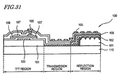
- FIG. 31 is a cross-sectional view showing the construction of a lower substrate 100 of a conventional FFS mode transflective-type liquid crystal display device which is described in Patent Document 1.
- the lower substrate 100 includes a TFT region, a transmission region, and a reflection region.
- a gate electrode 103, an active layer 106, a source/drain electrode 107, and the like are formed on an organic resin film 101.
- a counter electrode 102, a pixel electrode 105, and the like are formed in the transmission region and the reflection region.
- a plurality of slits are formed in the pixel electrode 105, such that the orientation of liquid crystal (not shown) which is disposed on the lower substrate 100 is controlled in accordance with a voltage or an electric field which is applied between electrode portions interposed between slits and the counter electrode 102.
- a reflector 109 for reflecting incident light is provided.
- the counter electrode 102 is provided in contact with the substrate 110; however, in the reflection region, the counter electrode 102 is formed on the organic resin film 101 disposed on the substrate 110.
- An emboss pattern is formed by etching on an upper face of the organic resin film 101 in the reflection region, and a plurality of protrusions (or recesses) are formed on the counter electrode 102 so as to conform to the shape of this upper face.
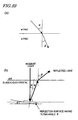
- the reflection-type liquid crystal display device or the transflective-type liquid crystal display device in order to perform bright displaying by utilizing reflected light, it is necessary to allow incident light entering at various azimuths to be more uniformly and efficiently reflected by the reflection surface of the reflective layer across the entire display surface. For this purpose, it is better if the reflection surface has moderate ruggednesses rather than being a complete plane.
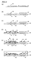
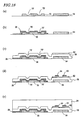
- FIG. 32 is a diagram showing a relationship between the tilt of a reflection surface and reflected light.
- FIG. 32(a) shows a relationship between an incident angle a and an outgoing angle 13 when light enters a medium b having a refractive index Nb from a medium a having a refractive index Na.
- Nb a refractive index
- Na * sin ⁇ Nb * sin ⁇
- FIG. 32(b) is a diagram showing a relationship between incident light and reflected light when incident light perpendicularly entering the display surface of a liquid crystal display device is reflected from a reflection surface which is tilted by ⁇ with respect to the display surface (or the substrate). As shown in the figure, the incident light perpendicularly entering the display surface is reflected from the reflection surface which is tilted by angle ⁇ with respect to the display surface, and goes out in a direction of an outgoing angle ⁇ .
- FIG. 3 1 it is described that, in the reflection region of the lower substrate 100, ruggednesses are formed on the counter electrode 102 in accordance with the emboss pattern which is provided on the surface of the organic resin film 101, but no consideration is given as to adjusting the tilting angle of the reflector 109 in order to efficiently utilize reflected light, or ensuring that the tilt of the surface of the reflector 109 is 20 degrees or less.
- the present invention has been made in view of the above problems, and an objective thereof is to provide with a good production efficiency a reflection-type liquid crystal display device and a transflective-type liquid crystal display device having a high image quality and being capable of efficiently utilizing reflected light.
- a liquid crystal display device is a liquid crystal display device comprising the features of claim 1.
- the second electrode includes a protrusion, a recess, or an aperture
- the reflective layer includes a protrusion, a recess, or a level difference which is formed in accordance with the protrusion, recess, or aperture of the second electrode.
- One embodiment comprises, under the reflective layer, a semiconductor layer made of a same material as a semiconductor portion of the transistor, the semiconductor layer including a protrusion, a recess, or an aperture, wherein, the reflective layer includes a protrusion, a recess, or a level difference which is formed in accordance with the protrusion, recess, or aperture of the semiconductor layer.
- the reflective layer is made of a same material as that of a source electrode or a drain electrode of the transistor.
- an insulating layer is formed between the metal layer and the second electrode; and a contact hole electrically connecting the metal layer and the second electrode is formed in the insulating layer.
- the reflective layer includes an aperture.
- the second electrode is formed over the metal layer, and includes a protrusion, a recess, or a level difference which is formed in accordance with the protrusion, recess, or aperture of the metal layer.
- the second electrode is formed under the metal layer, and includes a protrusion, a recess, or an aperture; and the metal layer includes a protrusion, a recess, or a level difference which is formed in accordance with the protrusion, recess, or aperture of the second electrode.
- the first electrode is a pixel electrode
- the second electrode is a counter electrode formed under the first electrode
- the first electrode is a pixel electrode
- the second electrode is a counter electrode formed on a same plane as the first electrode
- Another liquid crystal display device representing background art to the present invention is a liquid crystal display device comprising: a first substrate and a second substrate between which liquid crystal is interposed; a first electrode and a second electrode formed of the first substrate for applying a voltage for controlling an orientation of the liquid crystal; a transistor having an electrode which is electrically connected to the first electrode; a metal layer formed on the first substrate for reflecting incident light toward a display surface, the metal layer including a protrusion, a recess, or an aperture, wherein, the metal layer is made of a same material as that of a gate electrode of the transistor.
- the first electrode is a pixel electrode; and the second electrode is a counter electrode formed over the metal layer.
- the first electrode is a pixel electrode
- the second electrode is a counter electrode being formed under the metal layer and including a protrusion, a recess, or an aperture
- the metal layer includes a protrusion, a recess, or a level difference which is formed in accordance with the protrusion, recess, or aperture of the second electrode.
- the first electrode is a pixel electrode
- the second electrode is a counter electrode formed on a same plane as the first electrode
- Another liquid crystal display device representing background art to the present invention is a liquid crystal display device having: a reflection region including a reflective layer for reflecting incident light toward a display surface; and a TFT region, the liquid crystal display device comprising: a first substrate and a second substrate between which liquid crystal is interposed; a first electrode and a second electrode formed on the first substrate for applying a voltage for controlling an orientation of the liquid crystal; and a transistor being formed in the TFT region and having a gate layer, a semiconductor layer, a source electrode, and a drain electrode, wherein, in the reflection region, a layer is formed which is made of a same material as that of the gate layer, the semiconductor layer, the source electrode, or the drain electrode of the transistor, the layer including a protrusion, a recess, or an aperture.
- the reflective layer is made of a same material as that of the gate layer, the source electrode, or the drain electrode of the transistor, and includes a protrusion, a recess, an aperture, or a level difference.
- a production method for a liquid crystal display device is a production method for a liquid crystal display device including the features of claim 11.
- the first metal layer or the second metal layer constitutes the reflective layer.
- a semiconductor layer including a protrusion, a recess, or an aperture is formed from a same material as that of the semiconductor layer in the TFT region.
- a layer which is made of the same material as that of a layer composing a transistoror, or a layer which is stacked in the same step as that of a layer composing a transistor is formed, and in accordance with the shape of this layer, a protrusion, a recess, or a level difference is formed in a reflective layer (including any layer having the function as a reflective layer). Therefore, a reflection-type liquid crystal display device and a transflective-type liquid crystal display device having a high image quality and being capable of efficiently utilizing reflected light can be provided with a good production efficiency.
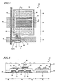
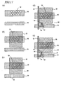
- FIG. 1 is a diagram schematically showing a cross-sectional shape of a liquid crystal display device 10 of the present embodiment, which is a cross-sectional view showing the construction of one pixel among a plurality of pixels which are disposed in a matrix shape in the liquid crystal display device 10.
- the liquid crystal display device 10 of the present embodiment is an FFS mode transflective-type liquid crystal display device adopting an active matrix method. As shown in FIG. 1 , the liquid crystal display device 10 includes a TFT (Thin Film Transistor) substrate (first substrate) 12, a counter substrate (second substrate) 14 including color filters (CFs) and the like, and a liquid crystal layer 18 containing liquid crystal 16 which is sealed between the TFT substrate 12 and the counter substrate 14.
- TFT Thin Film Transistor
- the TFT substrate 12 includes a transparent substrate 22, an interlayer insulating layer (PAS) 24, a pixel electrode (first electrode) 26, and a counter electrode (common.electrode or lower electrode) 28 disposed below the pixel electrode 26, and has a reflection section 30 and a TFT section 32.
- the pixel electrode 26 is electrically connected to a drain electrode of a TFT which is formed in the TFT section 32, and as a voltage or electric field is applied to the liquid crystal 16 by the pixel electrode 26 and the counter electrode 28, the orientation of the liquid crystal 16 is controlled with respect to each pixel, thereby performing display.
- gate lines scanning lines
- source lines signal lines
- Cs lines storage capacitor electrode lines
- the counter substrate 14 includes a transparent substrate 34, a CF layer (color filter layer) 36, and the like.
- the upper face of the transparent substrate 34 serves as a display surface 40 of the liquid crystal display device.
- the TFT substrate 12 and the counter substrate 14 each include optical film layers such as an alignment film and a polarizer, those are omitted from illustration herein.
- a region where the reflection section 30 is formed is referred to as a reflection region 42
- a region where the TFT section 32 is formed is referred to as a TFT region 44.
- the reflection region 42 light entering from the display surface 40 is reflected by the reflective layer in the reflection section 30, and travels through the liquid crystal layer 18 and the counter substrate 14 so as to go out from the display surface 40 as reflected light 43.
- the liquid crystal display device 10 has transmission regions 46 which are formed in regions other than the reflection regions 42 and the TFT region 44. In the transmission regions 46, light which is emitted from a light source 48 in the liquid crystal display device 10 travels through the TFT substrate 12, the liquid crystal layer 18, and the counter substrate 14 so as to go out from the display surface 40 as transmitted light 49.
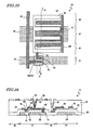
- FIG. 2 is a plan view schematically showing the construction of the TFT substrate 12 in one pixel among the plurality of pixels which are disposed in a matrix shape in the liquid crystal display device 10.
- a pixel 50 includes the reflection region 42, the TFT region 44, and the transmission region 46 mentioned above.
- source lines 52 extend along the column direction (up-down direction in the figure) of the plurality of pixels disposed in a matrix shape
- gate lines (gate metal layers) 54 extend along the row direction (right-left direction in the figure).
- a Cs line also referred to as a metal layer or a Cs metal layer
- Cs metal layer also referred to as a metal layer or a Cs metal layer
- a TFT 60 is formed in the TFT section 32 of the TFT region 44, whereas the counter electrode 28, the pixel electrode 26, and the like are formed in the transmission region 46.
- the Cs line 56, the counter electrode 28, the reflective layer 61, the pixel electrode 26, and the like, which are the elements of the reflection section 30 as shown in FIG. 1 are formed.
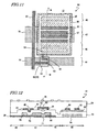
- FIG. 3 is a cross-sectional view schematically showing an A-A' cross section of the TFT substrate 12 shown in FIG. 2 .
- an insulating layer 58 is formed on the gate line (gate electrode) 54, and a semiconductor layer 62 is formed on the insulating layer 58.
- the semiconductor layer 62 is composed of an intrinsic amorphous silicon layer (Si(i)layer) and an n + amorphous silicon layer (Si (n + ) layer) doped with phosphorus, for example.
- a source electrode 63 and a drain electrode 64 are formed on the semiconductor layer 62, such that, as shown in FIG. 2 , the source electrode 63 is electrically connected to the source line 52, whereas the drain electrode 64 is electrically connected to the pixel electrode 26 via a contact hole 65 formed in the interlayer insulating layer 24.
- the Cs metal layer (also referred to as metal layer or Cs line) 56 is formed from the same member as the gate line (gate electrode) 54.
- the insulating layer 58, the counter electrode 28, the semiconductor layer 62, the reflective layer 61, the interlayer insulating layer 24, and the pixel electrode 26 are stacked.
- the Cs metal layer 56 is formed concurrently with and from the same member as the gate electrode 54 of the TFT 60; the semiconductor layer 62 as the semiconductor layer 62 of the TFT 60; and the reflective layer 61 as the source electrode 63 and drain electrode 64 of the TFT 60 .
- the Cs metal layer 56 has apertures 70
- the counter electrode 28 has apertures 71
- the semiconductor layer 62 is formed in an island shape from above an aperture 70 to inside the aperture 71.
- recesses 80, recesses 81, and protrusions 82 are formed so as to conform to the shapes of the apertures 70, the apertures 71, and the semiconductor layer 62, respectively. Because the semiconductor layer 62 is formed inside the apertures 71, level differences 83 are formed in the reflective layer 61.
- a contact hole 75 is formed in the insulating layer 58, such that the counter electrode 28 is electrically connected to the Cs metal layer 56 via the contact hole 75.
- protrusions or recesses may be formed on or in the Cs metal layer 56, and the Cs metal layer 56 may be formed in island shapes (it is assumed that each island portion of the Cs metal layer 56 also qualifies as "a protrusion of the Cs metal layer 56 ").
- protrusions or recesses may be formed on or in the counter electrode 28, and the counter electrode 28 may be formed in island shapes (it is assumed that each island portion of the counter electrode 28 qualifies as a "protrusion of the counter electrode 28" ).
- the semiconductor layer 62 may be formed as a layer having apertures, protrusions, or recesses. In either case, protrusions, recesses, or level differences are formed on or in the reflective layer 61 in accordance with the protrusions, recesses, and apertures of the Cs metal layer 56, the counter electrode 28, and the semiconductor layer 62.
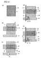
- FIG. 4 is a diagram schematically showing the shape of the reflective layer 61 as viewed from the display surface 40 side.
- the recesses 80 which are formed in accordance with the apertures 70 in the Cs metal layer 56, the recesses 81 which are formed in accordance with the apertures 71 in the counter electrode 28, the protrusions 82 which are formed in accordance with the protrusions of the semiconductor layer 62 (island shapes of the semiconductor layer 62 ), and the recesse 85 which is formed in accordance with the contact hole 75 in the insulating layer 58 are formed in the reflective layer 61.
- a level difference 83 is formed at each portion where a recess 81 and a protrusion 82 overlap.
- each of the recesses 80, recesses 81, and protrusions 82 are illustrated for ease of understanding the construction, the numbers of the recesses 80, recesses 81, and protrusions 82 are not limited to the illustrated numbers; more of them may be formed.
- a plurality of recesses, protrusions, or level differences are formed in or on the reflective layer 61. Since the corner portions and slopes of such recesses or the like include many faces whose angles with respect to the substrate are 20 degrees or less (effective reflection surfaces), reflected light can be effectively utilized. Moreover, since a multitude of faces having respectively different tilting angles are formed in the corner portions of the recesses or the like, reflected light is prevented from heading only in a fixed direction. Therefore, by forming more recesses or the like, it becomes possible to obtain reflected light which expands in a broader range.
- the reflective layer 61 is formed so as to conform to the shapes of the plurality of layers which are located below the reflective layer 61, more recesses or the like can be easily formed in the reflective layer 61, and shapes can be easily formed in which a plurality of recesses or the like overlap. Therefore, more effective reflection surfaces can be easily formed on the surface of the reflective layer 61.
- the reflective layer 61 is formed so as to conform to the shapes of a layer which are formed concurrently with and from the same material of a layer composing the TFT 60, there is no need to separately add a stacking step, a photolithography step, or the like in order to form the recesses or the like. Therefore, it is possible to provide a liquid crystal display device having a good reflection efficiency with a good production efficiency and at low cost. Moreover, since the shapes, depths, and slope tilting angles of the recesses or the like can be easily adjusted when shaping the respective layers composing the TFT 60, more effective reflection surfaces can be easily formed on the surface of the reflective layer 61.
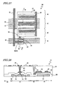
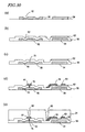
- FIG. 5 is plan views showing a production method for the TFT substrate 12, schematically showing the production steps of the portion illustrated in FIG. 2 .
- FIG. 6 is cross-sectional views for describing the production method for the TFT substrate 12, schematically showing the production steps of the portion illustrated in FIG. 3 .
- a thin metal film of Ta (tantalum) is formed on the transparent substrate having been cleaned.
- this thin metal film may be formed by using Al (aluminum), Ti (titanium), Cr (chromium), Mo (molybdenum), W (tungsten), or an alloy thereof, etc., or formed from a multilayer body of a layer of such materials and a nitride film.
- a resist film is formed on the thin metal film, and after forming a resist pattern through an exposure-development step, a dry etching is performed to form the gate electrode 54 and the Cs metal layer (first metal layer) 56.
- the thickness of the gate electrode 54 is 50 to 1000 nm, for example. Note that wet etching may be employed as the etching.
- a plurality of apertures 70 are formed in the Cs metal layer 56. In the case of forming the apertures 70, it is possible to adjust the tilting angle of the side face of each aperture 70 by using halftone exposure. Moreover, recesses (dents) may be formed instead of the apertures 70.
- the gate line 54 and the Cs line 56 shown in FIG. 2 are also formed concurrently from the same metal.
- the insulating layer 58 composed of SiN (silicon nitride) is formed on the entire substrate surface.
- the insulating layer 58 may also be composed of SiO 2 (silicon oxide), Ta 2 O 5 (tantalum oxide), Al 2 O 3 (aluminum oxide), or the like.
- the thickness of the insulating layer 58 is 100 to 600 nm, for example.
- an intrinsic amorphous silicon (a-Si) film (Si(i) film) and an n + a-Si film (Si(n + ) film) obtained by doping amorphous silicon with phosphorus (P) are formed.
- the thickness of the a-Si film is 20 to 300 nm, for example, and the thickness of the n + a-Si film is 20 to 100 nm, for example.
- these films are shaped by Photolithography technique, whereby the semiconductor layer 62 is formed.
- a plurality of annular shapes of semiconductor layer 62 are formed in island shapes, at positions overlapping the apertures 70 in the Cs metal layer 56.
- the contact hole 75 reaching the Cs metal layer 56 is formed in the insulating layer 58 by photolithography technique.
- a transparent electrode film of ITO, IZO, or the like is formed on the insulating layer 58 and the semiconductor layer 62 by sputtering technique or the like, and the resultant transparent electrode film is pattern-shaped by photolithography technique, whereby the counter electrode 28 is formed in the reflection region 42 and the transmission region 46.
- a plurality of apertures 71 are formed in the counter electrode 28. At least some of the plurality of apertures 71 are formed in positions overlapping the apertures 70 in the Cs metal layer 56 and the semiconductor layer 62, whereby recesses, protrusions, and level differences are formed on the surface of the counter electrode 28.
- a recess in accordance with the contact hole 75 is also formed in the counter electrode 28.
- a thin metal film of Al or the like is formed on the entire substrate surface by sputtering technique or the like, and a photolithography technique is employed to form the source electrode 63, the source line 52, the drain electrode 64, and the reflective layer (second metal layer) 61.
- the reflective layer 61 the recesses 80, the recesses 81, the protrusions 82, the level differences 83, and the recess 85 are formed, which conform to the shapes of the apertures 70 in the Cs metal layer 56, the semiconductor layer 62, the contact holes 75 in the insulating layer 58, and the apertures 71 in the counter electrode 28.
- the materials listed above as the materials for the gate electrode 54 can be used as the thin metal film.
- the thickness of the reflective layer 61 is 30 to 1000 nm, for example.
- a photosensitive acrylic resin is applied onto the substrate by spin-coating, whereby the interlayer insulating layer 24 is formed.
- the thickness of the interlayer insulating layer 24 is 0.3 to 5 ⁇ m, for example.
- the contact hole 65 is formed in the interlayer insulating layer 24 over the drain electrode 64.
- a thin film of SiN x , SiO 2 , or the like may be formed by P-CVD technique as a protection layer under the interlayer insulating layer 24, such is omitted from illustration herein.
- the thickness of the protection film is 50 to 1000 nm, for example.
- the pixel electrode 26 is formed on the interlayer insulating layer 24, whereby the TFT substrate 12 shown in FIG. 2 and FIG. 3 is completed.
- the pixel electrode 26 is obtained by stacking a transparent electrode film of ITO, IZO, or the like by sputtering technique or the like, and pattern-shaping the stacked transparent electrode film by photolithography technique.
- the pixel electrode 26 and the drain electrode 64 are electrically connected via the contact hole 65.
- apertures 70 in the Cs metal layer 56 are formed on the reflection surface, within the limitations of the masks and photoexposure during the production steps.
- the preferable sizes of the apertures 70, the apertures 71, and the island shapes of semiconductor layer 62 are defined by diameters of 2 to 10 ⁇ m.
- the liquid crystal display device of the present embodiment differs from the Embodiment 1 only with respect to a portion of the construction of the TFT substrate 12, and is identical to Embodiment 1 including the production method, effects, and the like, except for what is described below. Constituent elements which are identical to those of Embodiment 1 will be denoted by like reference numerals, and detailed descriptions thereof will be omitted.
- FIG. 7 is a plan view schematically showing the construction of the TFT substrate 12 corresponding to one pixel 50 of the liquid crystal display device 10 shown in FIG. 1 .
- FIG. 8 is a cross-sectional view schematically showing an A-A' cross section of the TFT substrate 12 shown in FIG. 7 .
- the counter electrode 28 is stacked on the Cs metal layer 56 so as to be in contact with the Cs metal layer 56.
- the insulating layer 58, the semiconductor layer 62, and the reflective layer 61 are stacked in this order.
- An aperture (gap or slit) 87 is formed in the reflective layer 61, such that the reflective layer 61 is divided into two portions because of the aperture 87.
- recesses 80 conforming to the apertures 70 in the Cs metal layer 56, recesses 81 conforming to the apertures 71 in the counter electrode 28, and protrusions 82 conforming to the island shapes of semiconductor layer 62 are formed in the reflective layer 61.
- the aperture 87 is formed also in the reflective layer 61 itself. This makes it possible to form a multitude of corner portions on the surface of the reflective layer 61. Note that a recess or protrusion may be formed instead of the aperture 87 in the reflective layer 61.
- FIG. 9 is plan views for describing a production method for the TFT substrate 12, schematically showing production steps for the portion shown in FIG. 7 .
- FIG. 10 is cross-sectional views for describing a production method for the TFT substrate 12, schematically showing production steps for the portion shown in FIG. 8 .
- a thin metal film of Ta (tantalum) or the like is formed on a transparent substrate having been cleaned.
- the Cs metal layer 56 having the gate electrode 54 and the apertures 70 is formed by photolithography technique.
- the gate line 54 and the Cs line 56 shown in FIG. 7 are also formed concurrently from the same metal.
- a transparent electrode film of ITO, IZO, or the like is formed on the substrate including the gate electrode 54 and the Cs metal layer 56 by sputtering technique or the like, and the transparent electrode film having been stacked is pattern-shaped by photolithography technique, whereby the counter electrode 28 is formed. At this time, a plurality of apertures 71 are formed in the counter electrode 28.
- a thin metal film of Al or the like is formed on the entire substrate surface by sputtering technique or the like, and a photolithography technique is employed to form the source electrode 63, the source line 52, the drain electrode 64, and the reflective layer 61.
- the reflective layer 61 the recess 80, the recess 81, and the protrusion 82 are formed so as to conform to the shapes of the apertures 70 in the Cs metal layer 56, the apertures 71 in the counter electrode 28, and the semiconductor layer 62.
- the aperture 87 is formed also in the reflective layer 61 itself.
- a photosensitive acrylic resin is applied onto the substrate by spin-coating, whereby the interlayer insulating layer 24 is formed.
- the contact hole 65 is formed in the interlayer insulating layer 24 over the drain electrode 64.
- the pixel electrode 26 is formed on the interlayer insulating layer 24, whereby the TFT substrate 12 shown in FIG. 7 and FIG. 8 is completed.
- the liquid crystal display device of the present embodiment differs from the Embodiment 1 only with respect to a portion of the construction of the TFT substrate 12, and is identical to Embodiment 1 including the production method, effects, and the like, except for what is described below.
- Constituent elements which are identical to those of Embodiment 1 will be denoted by like reference numerals, and detailed descriptions thereof will be omitted.
- FIG. 11 is a plan view schematically showing the construction of the TFT substrate 12 corresponding to one pixel 50 of the liquid crystal display device 10 shown in FIG. 1 .
- FIG. 12 is a cross-sectional view schematically showing an A-A' cross section of the TFT substrate 12 shown in FIG. 11 .
- the Cs metal layer 56 is stacked on the counter electrode 28 so as to be in contact with the counter electrode 28, the insulating layer 58 is stacked on the Cs metal layer 56, and the semiconductor layer 62 and the reflective layer 61 are stacked on the insulating layer 58.
- An aperture (gap or slit) 87 is formed in the reflective layer 61, such that the reflective layer 61 is divided into two portions because of the aperture 87.
- recesses 80 conforming to the apertures 70 in the Cs metal layer 56, recess 81 conforming to the apertures 71 in the counter electrode 28, and protrusions 82 conforming to the island shapes of semiconductor layer 62 are formed in the reflective layer 61.
- the aperture 87 is formed also in the reflective layer 61 itself. This makes it possible to form a multitude of corner portions on the surface of the reflective layer 61. Note that a recess or protrusion may be formed instead of the aperture 87 in the reflective layer 61.
- FIG. 13 is plan views for describing a production method for the TFT substrate 12, schematically showing production steps for the portion shown in FIG. 11 .
- FIG. 14 is cross-sectional views for describing a production method for the TFT substrate 12, schematically showing production steps for the portion shown in FIG. 12 .
- a transparent electrode film of ITO, IZO, or the like is stacked on a transparent substrate by sputtering technique or the like, and the transparent electrode film having been stacked is pattern-shaped by photolithography technique, whereby the counter electrode 28 is formed. At this time, a plurality of apertures 71 are formed in the counter electrode 28.
- a thin metal film of Ta (tantalum) or the like is formed by a method such as sputtering, and the Cs metal layer 56 having the gate electrode 54 and the apertures 70 is formed by photolithography technique. At this time, recesses conforming to the apertures 71 in the counter electrode 28 are formed in the Cs metal layer 56. Note that, in this step, the gate line 54 and the Cs line 56 shown in FIG. 11 are also formed concurrently from the same metal.
- the insulating layer 58 is stacked on the entire substrate surface, and after a semiconductor film is stacked thereupon, the stacked semiconductor film is shaped by photolithography technique, thereby forming the semiconductor layer 62.
- a thin metal film of Al or the like is formed on the entire substrate surface by sputtering technique or the like, and a photolithography technique is employed to form the source electrode 63, the source line 52, the drain electrode 64, and the reflective layer 61.
- the recesses 80, the recesses 81, and the protrusions 82 are formed so as to conform to the shapes of the apertures 70 in the Cs metal layer 56, the apertures 71 in the counter electrode 28, and the semiconductor layer 62.
- the aperture 87 is formed also in the reflective layer 61 itself.
- a photosensitive acrylic resin is applied onto the substrate by spin-coating, whereby the interlayer insulating layer 24 is formed.
- the contact hole 65 is formed in the interlayer insulating layer 24 over the drain electrode 64.
- the pixel electrode 26 is formed on the interlayer insulating layer 24, whereby the TFT substrate 12 shown in FIG. 11 and FIG. 12 is completed.
- the liquid crystal display device of the present embodiment differs from the Embodiment 1 only with respect to a portion of the construction of the TFT substrate 12, and is identical to Embodiment 1 including the production method, effects, and the like, except for what is described below. Constituent elements which are identical to those of Embodiment 1 will be denoted by like reference numerals, and detailed descriptions thereof will be omitted.
- FIG. 15 is a plan view schematically showing the construction of the TFT substrate 12 corresponding to one pixel 50 of the liquid crystal display device 10 shown in FIG. 1 .
- FIG. 16 is a cross-sectional view schematically showing an A-A' cross section of the TFT substrate 12 shown in FIG. 15 .
- the counter electrode 28 is stacked on the Cs metal layer 56 so as to be in contact with the Cs metal layer 56, and the insulating layer 58 is stacked on the counter electrode 28, but the semiconductor layer 62 and the reflective layer 61 are not stacked here (in the TFT region 44, similarly to Embodiment 1, the semiconductor layer 62, the source electrode 63 and the drain electrode 64 are formed).
- the Cs metal layer 56 functions as a reflective layer. Therefore, rather than apertures 70, recesses 70' are formed in the Cs metal layer 56, whereby a plurality of corner portions and slopes are formed in the surface of the Cs metal layer 56, thus improving the efficiency of utility of reflected light.
- FIG. 17 is plan views for describing a production method for the TFT substrate 12, schematically showing production steps for the portion shown in FIG. 15 .
- FIG. 18 is cross-sectional views for describing a production method for the TFT substrate 12, schematically showing production steps for the portion shown in FIG. 16 .
- a thin metal film of Ta (tantalum) or the like is formed, and the Cs metal layer 56 having the gate electrode 54 and the recesses 70' is formed by photolithography technique.
- the gate line 54 and the Cs line 56 shown in FIG. 15 are also formed concurrently from the same metal.
- a transparent electrode film of ITO, IZO, or the like is stacked by sputtering technique or the like, and the transparent electrode film having been stacked is pattern-shaped by photolithography technique, whereby the counter electrode 28 is formed. At this time, recesses conforming to the recesses 70' are formed in the counter electrode 28.
- the insulating layer 58 is stacked on the entire substrate surface, and a semiconductor film is stacked thereupon. Thereafter, the stacked semiconductor film is shaped by photolithography technique to form the semiconductor layer 62. However, herein, the semiconductor layer 62 is only formed in the TFT region 44.
- a thin metal film of Al or the like is stacked on the entire substrate surface by sputtering technique or the like, and a photolithography technique is employed to form the source electrode 63, the drain electrode 64, and the source line 52. At this time, any thin metal film that has been stacked on the reflection region 42 and the transmission region 46 is removed.
- a photosensitive acrylic resin is applied onto the substrate by spin-coating, whereby the interlayer insulating layer 24 is formed.
- the contact hole 65 is formed in the interlayer insulating layer 24 over the drain electrode 64.
- the pixel electrode 26 is formed on the interlayer insulating layer 24, whereby the TFT substrate 12 shown in FIG. 15 and FIG. 16 is completed.
- the liquid crystal display device of the present embodiment differs from the Embodiment 1 only with respect to a portion of the construction of the TFT substrate 12, and is identical to Embodiment 1 including the production method, effects, and the like, except for what is described below. Constituent elements which are identical to those of Embodiment 1 will be denoted by like reference numerals, and detailed descriptions thereof will be omitted.
- FIG. 19 is a plan view schematically showing the construction of the TFT substrate 12 corresponding to one pixel 50 of the liquid crystal display device 10 shown in FIG. 1 .
- FIG. 20 is a cross-sectional view schematically showing an A-A' cross section of the TFT substrate 12 shown in FIG. 19 .
- the Cs metal layer 56 is stacked on the counter electrode 28 so as to in contact with the counter electrode 28, and the insulating layer 58 is stacked on the Cs metal layer 56, but the semiconductor layer 62 and the reflective layer 61 are not stacked here (in the TFT region 44, similarly to Embodiment 1, the semiconductor layer 62, the source electrode 63, and the drain electrode 64 are formed).
- the Cs metal layer 56 functions as a reflective layer. Therefore, rather than apertures 70, recesses 70' are formed in the Cs metal layer 56. Moreover, apertures 71 are formed in the counter electrode 28. Therefore, recesses conforming to the apertures 71 are formed in addition to the recesses 70', so that a plurality of corner portions and slopes are formed on the surface of the Cs metal layer 56, thus improving the efficiency of utility of reflected light. Note that, herein, the Cs metal layer 56 also has the function of a counter electrode because the Cs metal layer 56 is in electrical contact with the counter electrode 28.
- FIG. 21 is plan views for describing a production method for the TFT substrate 12, schematically showing production steps for the portion shown in FIG. 19 .
- FIG. 22 is cross-sectional views for describing a production method for the TFT substrate 12, schematically showing production steps for the portion shown in FIG. 20 .
- a transparent electrode film of ITO, IZO, or the like is stacked by sputtering technique or the like, and the transparent electrode film having been stacked is pattern-shaped by photolithography technique, whereby the counter electrode 28 is formed.
- the apertures 71 are formed in the counter electrode 28.
- a thin metal film of Ta (tantalum) or the like is formed by a method such as sputtering, and the gate electrode 54 and the Cs metal layer 56 are formed by photolithography technique.
- the recesses 70' are formed in the Cs metal layer 56.
- recesses conforming to the apertures 71 in the counter electrode 28 are also formed in the Cs metal layer 56.
- the gate line 54 and the Cs line 56 shown in FIG. 19 are also formed concurrently from the same metal.
- the insulating layer 58 is stacked on the entire substrate surface, and a semiconductor film is stacked thereupon. Thereafter, the stacked semiconductor film is shaped by photolithography technique to form the semiconductor layer 62. However, herein, the semiconductor layer 62 is only formed in the TFT region 44.
- a thin metal film of Al or the like is stacked on the entire substrate surface by sputtering technique or the like, and a photolithography technique is employed to form the source electrode 63, the drain electrode 64, and the source line 52. At this time, any thin metal film that has been stacked on the reflection region 42 and the transmission region 46 is removed.
- a photosensitive acrylic resin is applied onto the substrate by spin-coating, whereby the interlayer insulating layer 24 is formed.
- the contact hole 65 is formed in the interlayer insulating layer 24 over the drain electrode 64.
- the pixel electrode 26 is formed on the interlayer insulating layer 24, whereby the TFT substrate 12 shown in FIG. 19 and FIG. 20 is completed.
- the liquid crystal display device of the present embodiment is an IPS mode transflective-type liquid crystal display device, whose overall construction is basically the same as that shown in FIG. 1 .
- it is different from the liquid crystal display device of Embodiment 1 in terms of the construction of the TFT substrate 12. Therefore, those constituents of the TFT substrate 12 which are different from of Embodiment 1 will be mainly described below, and the descriptions of any portion that is identical to Embodiment 1 will be omitted, including the production method, effects, and the like.
- constituent elements which are identical to those of Embodiment 1 will be denoted by like reference numerals, and descriptions thereof will be omitted.
- FIG. 23 is a plan view schematically showing the construction of the TFT substrate 12 corresponding to one pixel 50 of the liquid crystal display device of the present embodiment.
- FIG. 24 is a cross-sectional view schematically showing an A-A' cross section of the TFT substrate 12 shown in FIG. 23 .
- a pixel electrode 26 and a counter electrode 28' in interdigitated shapes each having a plurality of projections are formed, and orientation control of the liquid crystal is performed in accordance with a voltage which is applied between the projections of the pixel electrode 26 and the projections of the counter electrode 28'.
- the pixel electrode 26 is electrically connected to the drain electrode 64 of the TFT 60 via the contact hole 65 formed in the interlayer insulating layer 24, whereas the counter electrode 28' is electrically connected to the reflective layer 61 formed in the reflection region 42 via a contact hole 65' which is formed in the interlayer insulating layer 24.
- the Cs metal layer 56 having the apertures 70, the insulating layer 58, and the island shapes of semiconductor layer 62 are formed in this order from the bottom.
- the reflective layer 61 is electrically connected to the Cs metal layer 56 via the contact hole 75 which is formed in the insulating layer 58.
- the reflective layer 61 has recesses 80 which are formed in accordance with the apertures 70 in the Cs metal layer 56, protrusions 82 which are formed in accordance with the island shapes of semiconductor layer 62, level differences 83 which are formed in accordance with the apertures 70 and the semiconductor layer 62, and a recess 85 which is formed in accordance with the contact hole 75 in the interlayer insulating layer 24.
- recesses 80 which are formed in accordance with the apertures 70 in the Cs metal layer 56
- protrusions 82 which are formed in accordance with the island shapes of semiconductor layer 62
- level differences 83 which are formed in accordance with the apertures 70 and the semiconductor layer 62
- a recess 85 which is formed in accordance with the contact hole 75 in the interlayer insulating layer 24.
- FIG. 25 is plan views for describing a production method for the TFT substrate 12, schematically showing production steps for the portion shown in FIG. 23 .
- FIG. 26 is cross-sectional views for describing a production method for the TFT substrate 12, schematically showing production steps for the portion shown in. FIG. 24 .
- a thin metal film of Ta (tantalum) or the like is formed, and the gate electrode 54 and the Cs metal layer 56 are formed by photolithography technique. At this time, the apertures 70 are formed in the Cs metal layer 56. Note that, in this step, the gate line 54 and the Cs line 56 shown in FIG. 23 are also formed concurrently from the same metal.
- the insulating layer 58 is stacked on the entire substrate surface, and a semiconductor film is stacked thereupon. Thereafter, the stacked semiconductor film is shaped by photolithography technique to form the semiconductor layer 62.
- a plurality of island shapes of semiconductor layer 62 are formed in the reflection region 42, at least some of which overlap the apertures 70.
- the contact hole 75 is formed in the insulating layer 58 by photolithography technique or the like.
- a thin metal film of Al or the like is stacked on the entire substrate surface by sputtering technique or the like, and a photolithography technique is employed to form the source electrode 63, the drain electrode 64, the reflective layer 61, and the source line 52.
- the reflective layer 61 the recesses 80 conforming to the shapes of the apertures 70 in the Cs metal layer 56, the protrusions 82 conforming to the shapes of the island shapes of semiconductor layer 62, the level differences 83 conforming to the shapes of the apertures 70 and the semiconductor layer 62, and the recess 85 conforming to the shapes of the contact hole 75 in the interlayer insulating layer 24 are formed.
- a photosensitive acrylic resin is applied onto the substrate by spin-coating, whereby the interlayer insulating layer 24 is formed.
- the interlayer insulating layer 24 by photolithography technique or the like, the contact hole 65 is formed over the drain electrode 64, and the contact hole 65' is formed over the reflective layer 61.
- the transparent electrode film is pattern-shaped by photolithography technique to form the pixel electrode 26 and the counter electrode 28', whereby the TFT substrate 12 shown in FIG. 23 and FIG. 24 is completed.
- the liquid crystal display device of the present embodiment is an IPS mode transflective-type liquid crystal display device, and its construction is basically the same as that shown in FIG. 1 , except for the TFT substrate 12. Therefore, the construction of the TFT substrate 12 will be mainly described below, and the descriptions of any portion that is identical to Embodiment 1 will be omitted, including the production method, effects, and the like. Moreover, constituent elements which are identical to those of Embodiment 1 will be denoted by like reference numerals, and descriptions thereof will be omitted.
- FIG. 27 is a plan view schematically showing the construction of the TFT substrate 12 corresponding to one pixel 50 of the liquid crystal display device of the present embodiment.
- FIG. 28 is a cross-sectional view schematically showing an A-A' cross section of the TFT substrate 12 shown in FIG. 27 .
- a pixel electrode 26 and a counter electrode 28' in interdigitated shapes each having a plurality of projections are formed, and orientation control of the liquid crystal is performed in accordance with a voltage which is applied between the projections of the pixel electrode 26 and the projections of the counter electrode 28'.
- the pixel electrode 26 is electrically connected to the drain electrode 64 of the TFT 60 via a contact hole 65 which is formed in the interlayer insulating layer 24, whereas the counter electrode 28' is electrically connected to the reflective layer 61 formed in the reflection region 42 via a contact hole 65' which is formed in the interlayer insulating layer 24.
- the reflective layer 61 is formed only under a portion of the counter electrode 28 in Embodiment 7, a reflective layer's function of reflecting incident light toward the display surface pertains to the Cs metal layer 56 herein.
- the Cs metal layer 56 and the insulating layer 58 are formed in this order from the bottom.
- the semiconductor layer 62 is not formed in the reflection region 42.
- the reflective layer 61 is electrically connected to the Cs metal layer 56 via a contact hole 75 which is formed in the insulating layer 58. Therefore, the counter electrode 28' is electrically connected to the Cs metal layer 56 via the contact hole 65', the reflective layer 61, and the contact hole 75.
- the Cs metal layer 56 has a function as a reflective layer, recesses 70' are formed in the Cs metal layer 56, rather than apertures. Since the recesses 70 'are formed, a plurality of corner portion and slopes are formed on the surface of the reflective layer 61, thus improving the efficiency of utility of reflected light.
- FIG. 29 is plan views for describing a production method for the TFT substrate 12, schematically showing production steps for the portion shown in FIG. 27 .
- FIG. 30 is cross-sectional views for describing a production method for the TFT substrate 12, schematically showing production steps for the portion shown in FIG. 28 .
- a thin metal film of Ta (tantalum) or the like is formed, and the gate electrode 54 and the Cs metal layer 56 are formed by photolithography technique. At this time, the recesses 70' are formed in the Cs metal layer 56. Note that, in this step, the gate line 54 and the Cs line 56 shown in FIG. 27 are also formed concurrently from the same metal.
- the insulating layer 58 is stacked on the entire substrate surface, and a semiconductor film is stacked thereupon. Thereafter, the stacked semiconductor film is shaped by photolithography technique to form the semiconductor layer 62.
- any semiconductor film that has been stacked in the reflection region 42 is removed, and no semiconductor layer 62 is formed in the reflection region 42.
- the contact hole 75 is formed in the insulating layer 58 by photolithography technique or the like.
- a thin metal film of Al or the like is stacked on the entire substrate surface by sputtering technique or the like, and a photolithography technique is employed to form the source electrode 63, the drain electrode 64, the reflective layer 61, and the source line 52.
- the reflective layer 61 is formed only over the contact hole 75 so as to cover the contact hole 75.
- a photosensitive acrylic resin is applied onto the substrate by spin-coating, whereby the interlayer insulating layer 24 is formed.
- the interlayer insulating layer 24 by photolithography technique or the like, the contact hole 65 is formed over the drain electrode 64, and the contact hole 65' is formed over the reflective layer 61.
- the transparent electrode film is pattern-shaped by photolithography technique to form the pixel electrode 26 and the counter electrode 28', whereby the TFT substrate 12 shown in FIG. 27 and the FIG. 28 is completed.
- the plurality of apertures and recesses that are formed in the Cs metal layer 56 in the reflection region 42 are all circular as viewed perpendicularly to the substrate, some or all of these apertures and recesses may be formed in other shapes, e.g., ellipses or rectangles. Although it has been illustrated that a plurality of circular-island shapes of semiconductor layer 62 are formed in the reflection region 42, some or all of these may be formed in other shapes, e.g., ellipses or rectangles.
- apertures, recesses, protrusion, and the like may be formed by employing halftone exposure during the shaping of these layers.
- halftone exposure it becomes possible to easily adjust the tilting angles of the side faces of the apertures and the like to desired angles, and it becomes easy to provide more level differences inside the apertures and the like.
- slopes having more corner portions and desired tilting angles are formed in the reflective layer 61, thus improving the efficiency of utility of reflected light.
- the apertures and the like to be formed in the respective layers may be disposed in a manner of overlapping concentric circles, but more preferably, they may be disposed so that the edges of the apertures and the like overlap. In the case where the edges of the apertures and the like overlap, more complicated rugged structures are formed on the surface of the reflective layer 61, thus allowing the reflected light to be uniformly reflected in a broader range.
- the reflective layer 61 It is preferable that as many recesses, protrusions, and level differences as possible are formed in the reflective layer 61.
- sizes and shapes of the recesses or the like are not limited to those described above, but they may be formed into various shapes such as polygons other than rectangles, recesses or the like with sawtoothed edges, or combines thereof.
- a liquid crystal display device includes a large number of level differences and corner portions on the surface of a reflective layer, as well as a multitude of slopes with a tilting angle of 20 degrees or less, and therefore acquires reflection regions with broad effective reflection surfaces and excellent scattering characteristics.
- the level differences and corner portions on the reflection surface are formed based on layers which are shaped concurrently with the shaping of a gate layer of TFTs, a semiconductor layer, a source electrode, or a drain electrode, a reflection region having excellent reflection characteristics can be easily obtained without increasing the production steps. Therefore, a liquid crystal display device that is capable of uniform and high-brightness displaying can be inexpensively provided with a good production efficiency.
- the liquid crystal display device according to the present invention is formed by the above-described production method, it can be produced with the substantially the same material and steps as those of a transmission-type liquid crystal display device. Therefore, a liquid crystal display device with an excellent reflection efficiency can be provided at low cost.
- the liquid crystal display device encompasses display apparatuses, television sets, mobile phones, etc., in which a liquid crystal panel is utilized.
- a liquid crystal panel is utilized.
- the present embodiments employ transflective-type liquid crystal display devices as examples, a reflection-type liquid crystal display device or the like having a configuration similar to the aforementioned reflection section is also encompassed as an embodiment of the present invention.
- a transflective-type liquid crystal display device and a reflection-type liquid crystal display device of the FFS mode and the IPS mode having a high image quality can be provided at low cost.
- Liquid crystal display devices according to the present invention are suitably used for various liquid crystal display devices, and are suitably used for transflective-type liquid crystal display devices and reflection-type liquid crystal display devices which perform display by utilizing reflected light, e.g., mobile phones, onboard display devices such as car navigation systems, display devices of ATMs and vending machines, etc., portable display devices, laptop PCs, and the like.
Landscapes
- Physics & Mathematics (AREA)
- Nonlinear Science (AREA)
- Mathematical Physics (AREA)
- Chemical & Material Sciences (AREA)
- Crystallography & Structural Chemistry (AREA)
- General Physics & Mathematics (AREA)
- Optics & Photonics (AREA)
- Liquid Crystal (AREA)
Abstract
Claims (13)
- Dispositif d'affichage à cristaux liquides (10) comprenant :un premier substrat (12) et un second substrat (14) entre lesquels des cristaux liquides sont interposés ;une première électrode (26) et une seconde électrode (28) formées sur le premier substrat (12) pour appliquer une tension pour commander une orientation des cristaux liquides ;un transistor (60) comportant une électrode qui est électriquement reliée à la première électrode (26) ;une couche de métal (56) formée sur le premier substrat (12), la couche de métal (56) comportant une protubérance, une partie en retrait, ou une ouverture (70) ; etune couche réfléchissante (61) formée au-dessus de la couche de métal (56) dans le premier substrat (12), la couche réfléchissante (61) reflétant une lumière incidente vers une surface d'affichage (40), caractérisé en ce quela couche de métal (56) est faite d'une même matière que celle d'une électrode de grille (54) du transistor (60) ; etla couche réfléchissante (61) comporte une protubérance, une partie en retrait (80), ou une différence de niveau (83) qui est provoquée par la protubérance, la partie en retrait, ou l'ouverture (70) de la couche de métal (56).
- Dispositif d'affichage à cristaux liquides (10) selon la revendication 1, dans lequel,
la seconde électrode (28) comporte une protubérance, une partie en retrait, ou une ouverture (71) ; et
la couche réfléchissante (61) comporte une protubérance, une partie en retrait (81), ou une différence de niveau qui est provoquée par la protubérance, la partie en retrait, ou l'ouverture (71) de la seconde électrode (28). - Dispositif d'affichage à cristaux liquides (10) selon la revendication 1 ou 2, comprenant
sous la couche réfléchissante (61), une couche semi-conductrice (62) faite d'une même matière qu'une partie semi-conductrice (62) du transistor (60), la couche semi-conductrice (62) comportant une protubérance, une partie en retrait, ou une ouverture, dans lequel,
la couche réfléchissante (61) comporte une protubérance (82), une partie en retrait, ou une différence de niveau qui est provoquée par la protubérance, la partie en retrait, ou l'ouverture de la couche semi-conductrice (62). - Dispositif d'affichage à cristaux liquides (10) selon l'une quelconque des revendications 1 à 3, dans lequel la couche réfléchissante (61) est faite d'une même matière que celle d'une électrode de source (63) ou d'une électrode de drain (64) du transistor (60).
- Dispositif d'affichage à cristaux liquides (10) selon l'une quelconque des revendications 1 à 4, dans lequel une couche d'isolation (58) est formée entre la couche de métal (56) et la seconde électrode (28') ; et
un trou de contact (75) reliant électriquement la couche de métal (56) et la seconde électrode (28') est formé dans la couche d'Isolation (58). - Dispositif d'affichage à cristaux liquides (10) selon l'une quelconque des revendications 1 à 4, dans lequel la couche réfléchissante (61) comporte une ouverture (87).
- Dispositif d'affichage à cristaux liquides (10) selon l'une quelconque des revendications 1 à 5, dans lequel la seconde électrode (28) est formée au-dessus de la couche de métal (56), et comporte une protubérance, une partie en retrait, ou une différence de niveau qui est provoquée par la protubérance, la partie en retrait, ou l'ouverture de la couche de métal (56).
- Dispositif d'affichage à cristaux liquides (10) selon l'une quelconque des revendications 1 à 4, dans lequel,
la seconde électrode (28) est formée sous la couche de métal (56), et comporte une protubérance, une partie en retrait, ou une ouverture ; et
la couche de métal (56) comporte une protubérance, une partie en retrait, ou une différence de niveau qui est provoquée par la protubérance, la partie en retrait, ou l'ouverture de la seconde électrode (28). - Dispositif d'affichage à cristaux liquides (10) selon l'une quelconque des revendications 1 à 8, dans lequel la première électrode (26) est une électrode de pixel, et la seconde électrode (28) est une contre-électrode formée sous la première électrode (26).
- Dispositif d'affichage à cristaux liquides (10) selon la revendication 1, dans lequel la première électrode (26) est une électrode de pixel et la seconde électrode (28) est une contre-électrode formée sur un même plan que la première électrode (26).
- Procédé de production pour un dispositif d'affichage à cristaux liquides (10) comportant un premier substrat (12) et un second substrat (14) entre lesquels des cristaux liquides sont interposés et une première électrode (26) et une seconde électrode (28) pour appliquer une tension pour commander une orientation des cristaux liquides, le dispositif d'affichage à cristaux liquides comportant : une zone de réflexion (42) comportant une couche réfléchissante (61) pour refléter une lumière incidente vers une surface d'affichage (40) ; et une zone de TFT (44), le procédé de production comprenant les étapes de :(a) formation d'une couche de grille (54) dans la zone de TFT (44) ;(b) formation d'une couche semi-conductrice (62) au-dessus de la couche de grille (54) dans la zone de TFT (44) ; et(c) formation d'une électrode de source (63) et d'une électrode de drain (64) au-dessus de la couche semi-conductrice (62) dans la zone de TFT (44), dans lequel,à l'étape (a), une première couche de métal (56) comportant une protubérance, une partie en retrait, ou une ouverture (70) est formée dans la zone de réflexion (42), à partir d'une même matière que celle de la couche de grille (54) de la zone de TFT (44), et
à l'étape (c), une seconde couche de métal (61) comportant une protubérance, une partie en retrait, ou une ouverture est formée dans la zone de réflexion, d'une même matière que celle de l'électrode de source (63) ou de l'électrode de drain (64) dans la zone de TFT, et dans lequel
à l'étape (c), dans la seconde couche de métal (61), une protubérance, une partie en retrait (80), ou une différence de niveau, qui est provoquée par la protubérance, la partie en retrait, ou l'ouverture (70) de la première couche de métal (56), est formée. - Procédé de production pour un dispositif d'affichage à cristaux liquides selon la revendication 11, dans lequel la première couche de métal (56) ou la seconde couche de métal (61) constitue la couche réfléchissante.
- Procédé de production selon la revendication 11 ou 12, dans lequel, à l'étape (b), dans la zone de réflexion, une couche semi-conductrice (62) comportant une protubérance, une partie en retrait, ou une ouverture est formée d'une même matière que celle de la couche semi-conductrice (62) dans la zone de TFT (44).
Applications Claiming Priority (2)
| Application Number | Priority Date | Filing Date | Title |
|---|---|---|---|
| JP2007105996 | 2007-04-13 | ||
| PCT/JP2007/075147 WO2008129748A1 (fr) | 2007-04-13 | 2007-12-27 | Ecran à cristaux liquides et procédé de fabrication d'un écran à cristaux liquides |
Publications (3)
| Publication Number | Publication Date |
|---|---|
| EP2144109A1 EP2144109A1 (fr) | 2010-01-13 |
| EP2144109A4 EP2144109A4 (fr) | 2011-01-19 |
| EP2144109B1 true EP2144109B1 (fr) | 2012-05-23 |
Family
ID=39875286
Family Applications (1)
| Application Number | Title | Priority Date | Filing Date |
|---|---|---|---|
| EP07860369A Not-in-force EP2144109B1 (fr) | 2007-04-13 | 2007-12-27 | Ecran à cristaux liquides et procédé de fabrication d'un écran à cristaux liquides |
Country Status (5)
| Country | Link |
|---|---|
| US (1) | US8659726B2 (fr) |
| EP (1) | EP2144109B1 (fr) |
| JP (1) | JP5184517B2 (fr) |
| CN (1) | CN101663612B (fr) |
| WO (1) | WO2008129748A1 (fr) |
Families Citing this family (21)
| Publication number | Priority date | Publication date | Assignee | Title |
|---|---|---|---|---|
| WO2007015458A1 (fr) * | 2005-08-03 | 2007-02-08 | Sharp Kabushiki Kaisha | Dispositif d’affichage à cristaux liquides et dispositif électronique l’utilisant |
| CN101395525B (zh) * | 2006-03-23 | 2010-11-10 | 夏普株式会社 | 液晶显示装置 |
| US20090195741A1 (en) * | 2006-06-30 | 2009-08-06 | Yoshihito Hara | Liquid crystal display and method for manufacturing liquid crystal display |
| US8111356B2 (en) | 2006-09-12 | 2012-02-07 | Sharp Kabushiki Kaisha | Liquid crystal display panel provided with microlens array, method for manufacturing the liquid crystal display panel, and liquid crystal display device |
| CN101529318B (zh) * | 2006-10-18 | 2011-10-12 | 夏普株式会社 | 液晶显示装置和液晶显示装置的制造方法 |
| EP2085814A4 (fr) * | 2006-10-18 | 2010-05-19 | Sharp Kk | Écran à cristaux liquides et procédé de fabrication associé |
| CN101558350B (zh) * | 2006-12-14 | 2011-08-03 | 夏普株式会社 | 液晶显示装置和液晶显示装置的制造方法 |
| CN101589331B (zh) * | 2007-01-24 | 2011-06-22 | 夏普株式会社 | 液晶显示装置 |
| JP5048688B2 (ja) * | 2007-01-31 | 2012-10-17 | シャープ株式会社 | 液晶表示装置 |
| WO2009001508A1 (fr) * | 2007-06-26 | 2008-12-31 | Sharp Kabushiki Kaisha | Dispositif d'affichage à cristaux liquides et procédé de fabrication des dispositifs d'affichage à cristaux liquides |
| US8872180B2 (en) * | 2008-05-13 | 2014-10-28 | Sharp Kabushiki Kaisha | Liquid crystal display device and method for manufacturing liquid crystal display device |
| CN102637630B (zh) * | 2011-05-20 | 2014-02-19 | 京东方科技集团股份有限公司 | 阵列基板及其制造方法 |
| CN102650780B (zh) | 2011-05-30 | 2014-11-19 | 京东方科技集团股份有限公司 | 一种像素结构、液晶显示面板及制作方法 |
| US9075271B2 (en) | 2011-09-06 | 2015-07-07 | Japan Display Inc. | Liquid crystal display device |
| JP5824301B2 (ja) * | 2011-09-06 | 2015-11-25 | 株式会社ジャパンディスプレイ | 液晶表示装置 |
| JP5938181B2 (ja) * | 2011-09-06 | 2016-06-22 | 株式会社ジャパンディスプレイ | 液晶表示装置 |
| JP5816496B2 (ja) * | 2011-09-08 | 2015-11-18 | 株式会社ジャパンディスプレイ | 液晶表示装置 |
| US9250486B2 (en) | 2011-09-08 | 2016-02-02 | Japan Display Inc. | Liquid crystal display device |
| KR102004397B1 (ko) * | 2012-09-19 | 2019-07-29 | 삼성디스플레이 주식회사 | 표시 패널 |
| KR102343277B1 (ko) * | 2015-03-26 | 2021-12-24 | 삼성디스플레이 주식회사 | 반사층을 포함하는 표시 장치 |
| US10224407B2 (en) | 2017-02-28 | 2019-03-05 | Sandisk Technologies Llc | High voltage field effect transistor with laterally extended gate dielectric and method of making thereof |
Family Cites Families (98)
| Publication number | Priority date | Publication date | Assignee | Title |
|---|---|---|---|---|
| JPS5691277A (en) | 1979-12-25 | 1981-07-24 | Citizen Watch Co Ltd | Liquiddcrystal display panel |
| JPS58125084A (ja) | 1982-01-21 | 1983-07-25 | 株式会社東芝 | 液晶表示装置およびその製造方法 |
| JPS63296004A (ja) | 1987-05-28 | 1988-12-02 | Konica Corp | 光学フィルタ及び光学フィルタを内蔵したカラ−プル−フ作成装置 |
| JP2638630B2 (ja) | 1988-11-30 | 1997-08-06 | 富士写真フイルム株式会社 | ネガフィルム測定装置および自動カラー写真焼付装置 |
| JPH04372934A (ja) | 1991-06-24 | 1992-12-25 | Toshiba Corp | 液晶表示装置用アレイ基板の製造方法 |
| EP0536898B1 (fr) * | 1991-09-10 | 1997-07-02 | Sharp Kabushiki Kaisha | Dispositif d'affichage à cristal liquide de type de réflexion et procédé de fabrication |
| TW540747U (en) * | 1992-02-19 | 2003-07-01 | Sharp Kk | A reflective substrate and a liquid crystal display device using the same |
| JP3198625B2 (ja) | 1992-05-29 | 2001-08-13 | オムロン株式会社 | マイクロレンズアレイ基板とその製造方法及び同基板を用いた画像表示装置 |
| JPH06258637A (ja) * | 1993-03-04 | 1994-09-16 | Sony Corp | 液晶表示装置 |
| JPH06331831A (ja) | 1993-05-25 | 1994-12-02 | Sekisui Chem Co Ltd | 光制御シートおよびこれを備えた面状発光装置 |
| JPH08190089A (ja) | 1995-01-10 | 1996-07-23 | Rohm Co Ltd | 液晶表示装置 |
| JP2990046B2 (ja) | 1995-08-16 | 1999-12-13 | 日本電気株式会社 | 反射型液晶表示装置及びその製造方法 |
| JPH0964366A (ja) | 1995-08-23 | 1997-03-07 | Toshiba Corp | 薄膜トランジスタ |
| JP3149793B2 (ja) * | 1996-07-22 | 2001-03-26 | 日本電気株式会社 | 反射型液晶表示装置及びその製造方法 |
| KR100392909B1 (ko) | 1997-08-26 | 2004-03-22 | 엘지.필립스 엘시디 주식회사 | 박막트랜지스터및그의제조방법 |
| JP3666181B2 (ja) | 1997-03-21 | 2005-06-29 | ソニー株式会社 | 反射型兼透過型表示装置 |
| TW509808B (en) | 1997-06-12 | 2002-11-11 | Sharp Kk | Liquid crystal display device |
| US6330047B1 (en) * | 1997-07-28 | 2001-12-11 | Sharp Kabushiki Kaisha | Liquid crystal display device and method for fabricating the same |
| JPH11109390A (ja) | 1997-09-30 | 1999-04-23 | Toshiba Corp | 液晶表示装置 |
| JP4044187B2 (ja) * | 1997-10-20 | 2008-02-06 | 株式会社半導体エネルギー研究所 | アクティブマトリクス型表示装置およびその作製方法 |
| JPH11133399A (ja) * | 1997-10-27 | 1999-05-21 | Hitachi Ltd | 反射型液晶表示装置とその製造方法 |
| JPH11237625A (ja) | 1998-02-23 | 1999-08-31 | Alps Electric Co Ltd | フォトマスクおよびこれを用いた凹凸体の製造方法 |
| JP3019831B2 (ja) * | 1998-03-11 | 2000-03-13 | 日本電気株式会社 | 反射型液晶表示装置及びその製造方法 |
| JP3700387B2 (ja) | 1998-04-15 | 2005-09-28 | セイコーエプソン株式会社 | 液晶表示装置、液晶表示装置の駆動方法及び電子機器 |
| US6839108B1 (en) | 1998-05-16 | 2005-01-04 | Semiconductor Energy Laboratory Co., Ltd. | Liquid crystal display device and method of manufacturing the same |
| JPH11337961A (ja) * | 1998-05-26 | 1999-12-10 | Sharp Corp | 反射型液晶表示装置およびその製造方法 |
| JP2000010124A (ja) | 1998-06-22 | 2000-01-14 | Ricoh Co Ltd | 反射型液晶表示装置およびその製造方法 |
| JP2000047200A (ja) * | 1998-07-31 | 2000-02-18 | Hitachi Ltd | 拡散反射板とそれを用いた液晶表示装置およびその製法 |
| US6992718B1 (en) * | 1998-08-31 | 2006-01-31 | Matsushita Electric Industrial Co., Ltd. | Illuminating apparatus, display panel, view finder, video display apparatus, and video camera mounting the elements |
| US6287899B1 (en) | 1998-12-31 | 2001-09-11 | Samsung Electronics Co., Ltd. | Thin film transistor array panels for a liquid crystal display and a method for manufacturing the same |
| JP3916334B2 (ja) | 1999-01-13 | 2007-05-16 | シャープ株式会社 | 薄膜トランジスタ |
| JP2000329906A (ja) | 1999-05-21 | 2000-11-30 | Seiko Epson Corp | マイクロレンズアレイ基板とその製造方法 |
| CN1254710C (zh) * | 1999-07-07 | 2006-05-03 | 松下电器产业株式会社 | 半透射型液晶显示装置 |
| KR100407413B1 (ko) * | 1999-07-19 | 2003-11-28 | 마쯔시다덴기산교 가부시키가이샤 | 반사판 및 그 제조방법, 및 반사판을 구비한 반사형표시소자 및 그 제조방법 |
| US6909481B2 (en) | 2000-11-07 | 2005-06-21 | Seiko Epson Corporation | Liquid crystal display and electronic appliance |
| TW578028B (en) | 1999-12-16 | 2004-03-01 | Sharp Kk | Liquid crystal display and manufacturing method thereof |
| JP4372934B2 (ja) | 2000-01-18 | 2009-11-25 | 三菱化工機株式会社 | バスケット型遠心濾過装置及び遠心濾過方法 |
| JP2001201619A (ja) | 2000-01-21 | 2001-07-27 | Matsushita Electric Ind Co Ltd | 反射板及び反射型液晶表示パネル、並びにその製造方法。 |
| JP2001281698A (ja) | 2000-03-30 | 2001-10-10 | Advanced Display Inc | 電気光学素子の製法 |
| US6873384B2 (en) | 2000-04-17 | 2005-03-29 | Matsushita Electric Industrial Co., Ltd. | Reflection board, reflection tyre liquid crystal display unit and production method therefor, optical member, display unit, illuminating device, display board, and undulatory member |
| US6747289B2 (en) * | 2000-04-27 | 2004-06-08 | Semiconductor Energy Laboratory Co., Ltd. | Semiconductor device and method of fabricating thereof |
| US6900084B1 (en) * | 2000-05-09 | 2005-05-31 | Semiconductor Energy Laboratory Co., Ltd. | Semiconductor device having a display device |
| JP2001337323A (ja) | 2000-05-29 | 2001-12-07 | Mitsubishi Electric Corp | 反射型液晶表示装置とその製造方法、およびそれを用いた携帯機器 |
| WO2002010806A1 (fr) * | 2000-07-28 | 2002-02-07 | Matsushita Electric Industrial Co., Ltd. | Feuille reflechissante, son procede de fabrication et unite d'affichage y faisant appel |
| JP3712637B2 (ja) | 2000-08-11 | 2005-11-02 | シャープ株式会社 | 液晶表示装置およびその欠陥修正方法 |
| JP2002062665A (ja) | 2000-08-16 | 2002-02-28 | Koninkl Philips Electronics Nv | 金属膜の製造方法、該金属膜を有する薄膜デバイス、及び該薄膜デバイスを備えた液晶表示装置 |
| JP3904828B2 (ja) * | 2000-12-07 | 2007-04-11 | 株式会社日立製作所 | 液晶表示装置 |
| TW571165B (en) | 2000-12-15 | 2004-01-11 | Nec Lcd Technologies Ltd | Liquid crystal display device |
| JP2002184908A (ja) * | 2000-12-19 | 2002-06-28 | Sony Corp | 電子回路装置 |
| JP3875125B2 (ja) | 2001-04-11 | 2007-01-31 | シャープ株式会社 | 液晶表示装置 |
| JP2002323705A (ja) * | 2001-04-25 | 2002-11-08 | Seiko Epson Corp | 電気光学装置および電子機器 |
| JP5093709B2 (ja) * | 2001-08-22 | 2012-12-12 | Nltテクノロジー株式会社 | 液晶表示装置 |
| JP4111785B2 (ja) | 2001-09-18 | 2008-07-02 | シャープ株式会社 | 液晶表示装置 |
| TW517393B (en) | 2001-11-09 | 2003-01-11 | Prime View Int Co Ltd | TFT LCD structure with protrusion structure and its manufacturing method |
| JP2002236283A (ja) | 2001-12-03 | 2002-08-23 | Omron Corp | 画像表示装置とその製造方法、及びマイクロレンズアレイ基板とその製造方法 |
| TWI292849B (fr) | 2001-12-31 | 2008-01-21 | Prime View Int Corp Ltd | |
| JP2003222854A (ja) | 2002-01-31 | 2003-08-08 | Casio Comput Co Ltd | 液晶表示装置およびその製造方法 |
| JP4009776B2 (ja) | 2002-02-06 | 2007-11-21 | カシオ計算機株式会社 | 液晶表示装置およびその製造方法 |
| JP3900975B2 (ja) | 2002-03-06 | 2007-04-04 | オムロン株式会社 | 反射板、反射型表示装置および電子機器並びに光反射方法および画像表示方法 |
| JP4004835B2 (ja) | 2002-04-02 | 2007-11-07 | 株式会社アドバンスト・ディスプレイ | 薄膜トランジスタアレイ基板の製造方法 |
| JP4029663B2 (ja) | 2002-05-22 | 2008-01-09 | セイコーエプソン株式会社 | 半透過反射型液晶装置、およびそれを用いた電子機器 |
| JP4117148B2 (ja) * | 2002-05-24 | 2008-07-16 | 日本電気株式会社 | 半透過型液晶表示装置 |
| JP4133088B2 (ja) | 2002-08-01 | 2008-08-13 | Nec液晶テクノロジー株式会社 | 液晶表示装置 |
| JP2004258366A (ja) | 2003-02-26 | 2004-09-16 | Seiko Epson Corp | 電気光学装置、電気光学装置の製造方法および電子機器 |
| JP2004264653A (ja) | 2003-03-03 | 2004-09-24 | Seiko Epson Corp | 電気光学基板及びその製造方法、電気光学装置、電子機器 |
| JP2004325503A (ja) | 2003-04-21 | 2004-11-18 | Sharp Corp | 液晶表示装置 |
| CN1302322C (zh) * | 2003-11-24 | 2007-02-28 | 友达光电股份有限公司 | 具有多域垂直配向模式的晶体管液晶显示器 |
| JP2005157105A (ja) | 2003-11-27 | 2005-06-16 | Sanyo Electric Co Ltd | 半透過型液晶表示装置 |
| JP2005173037A (ja) | 2003-12-09 | 2005-06-30 | Fujitsu Display Technologies Corp | 液晶表示装置及びその製造方法 |
| JP4338511B2 (ja) | 2003-12-24 | 2009-10-07 | シャープ株式会社 | 液晶表示装置 |
| JP4401221B2 (ja) | 2003-12-25 | 2010-01-20 | シャープ株式会社 | 液晶表示装置の製造方法 |
| JP2005195733A (ja) | 2004-01-05 | 2005-07-21 | Hitachi Maxell Ltd | マイクロレンズアレイを有する透明基板及び液晶表示装置 |
| SG114747A1 (en) | 2004-02-25 | 2005-09-28 | Mitsubishi Gas Chemical Co | Etching composition for laminated film including reflective electrode and method for forming laminated wiring structure |
| JP4499481B2 (ja) * | 2004-06-03 | 2010-07-07 | 富士通株式会社 | 液晶表示装置及びその製造方法 |
| JP4606822B2 (ja) | 2004-09-10 | 2011-01-05 | シャープ株式会社 | 半透過型液晶表示装置の製造方法 |
| JP2006098525A (ja) | 2004-09-28 | 2006-04-13 | Hitachi Maxell Ltd | 光学部品及びその製造方法並びに当該方法で製造された光学部品を有する液晶表示装置 |
| JP4578958B2 (ja) * | 2004-12-16 | 2010-11-10 | シャープ株式会社 | 液晶表示装置 |
| JP2006184673A (ja) | 2004-12-28 | 2006-07-13 | Seiko Epson Corp | 液晶装置及び電子機器 |
| JP4138759B2 (ja) * | 2005-02-03 | 2008-08-27 | セイコーエプソン株式会社 | 液晶表示装置および電子機器 |
| JP2006220711A (ja) | 2005-02-08 | 2006-08-24 | Seiko Epson Corp | 液晶装置、液晶装置用基板及び電子機器 |
| JP2006220922A (ja) | 2005-02-10 | 2006-08-24 | Sony Corp | 表示装置およびその製造方法 |
| JP4440150B2 (ja) | 2005-03-16 | 2010-03-24 | シャープ株式会社 | 液晶表示装置及びその製造方法 |
| JP4446307B2 (ja) | 2005-04-08 | 2010-04-07 | シャープ株式会社 | 積層フィルムの製造方法、積層フィルム、および表示装置の製造方法 |
| KR100648223B1 (ko) * | 2005-05-11 | 2006-11-24 | 비오이 하이디스 테크놀로지 주식회사 | 반투과형 프린지 필드 스위칭 모드 액정표시장치 |
| US7705937B2 (en) * | 2005-06-30 | 2010-04-27 | Nec Lcd Technologies, Ltd. | Transflective liquid crystal display device |
| JP4039444B2 (ja) | 2005-07-15 | 2008-01-30 | エプソンイメージングデバイス株式会社 | 液晶表示装置及び電子機器 |
| JP4919644B2 (ja) | 2005-10-04 | 2012-04-18 | 三菱電機株式会社 | 液晶表示装置 |
| CN102331638B (zh) * | 2005-12-05 | 2015-11-25 | 株式会社半导体能源研究所 | 液晶显示器 |
| JP4637815B2 (ja) * | 2005-12-05 | 2011-02-23 | 株式会社半導体エネルギー研究所 | 液晶表示装置及び電子機器 |
| WO2007129518A1 (fr) * | 2006-05-01 | 2007-11-15 | Sharp Kabushiki Kaisha | Dispositif d'affichage à cristaux liquides et procédé de fabrication du dispositif d'affichage à cristaux liquides |
| US8294854B2 (en) * | 2006-05-01 | 2012-10-23 | Sharp Kabushiki Kaisha | Liquid crystal display comprising a reflection region having first, second and third recesses and method for manufacturing the same |
| US7847904B2 (en) * | 2006-06-02 | 2010-12-07 | Semiconductor Energy Laboratory Co., Ltd. | Liquid crystal display device and electronic appliance |
| JP2008009425A (ja) * | 2006-06-02 | 2008-01-17 | Semiconductor Energy Lab Co Ltd | 液晶表示装置及び電子機器 |
| JP2007329099A (ja) | 2006-06-09 | 2007-12-20 | Sharp Corp | 面光源装置および液晶表示装置 |
| CN101529318B (zh) * | 2006-10-18 | 2011-10-12 | 夏普株式会社 | 液晶显示装置和液晶显示装置的制造方法 |
| JP2008242307A (ja) | 2007-03-28 | 2008-10-09 | Sharp Corp | マイクロレンズアレイ付き液晶表示パネル |
| WO2009001508A1 (fr) * | 2007-06-26 | 2008-12-31 | Sharp Kabushiki Kaisha | Dispositif d'affichage à cristaux liquides et procédé de fabrication des dispositifs d'affichage à cristaux liquides |
| JP5333328B2 (ja) | 2010-04-12 | 2013-11-06 | 日立電線株式会社 | コネクタ |
-
2007
- 2007-12-27 JP JP2009510745A patent/JP5184517B2/ja not_active Expired - Fee Related
- 2007-12-27 EP EP07860369A patent/EP2144109B1/fr not_active Not-in-force
- 2007-12-27 CN CN2007800525741A patent/CN101663612B/zh not_active Expired - Fee Related
- 2007-12-27 WO PCT/JP2007/075147 patent/WO2008129748A1/fr not_active Ceased
- 2007-12-27 US US12/595,782 patent/US8659726B2/en not_active Expired - Fee Related
Also Published As
| Publication number | Publication date |
|---|---|
| EP2144109A4 (fr) | 2011-01-19 |
| JP5184517B2 (ja) | 2013-04-17 |
| CN101663612B (zh) | 2011-07-27 |
| US8659726B2 (en) | 2014-02-25 |
| US20100053517A1 (en) | 2010-03-04 |
| JPWO2008129748A1 (ja) | 2010-07-22 |
| CN101663612A (zh) | 2010-03-03 |
| WO2008129748A1 (fr) | 2008-10-30 |
| EP2144109A1 (fr) | 2010-01-13 |
Similar Documents
| Publication | Publication Date | Title |
|---|---|---|
| EP2144109B1 (fr) | Ecran à cristaux liquides et procédé de fabrication d'un écran à cristaux liquides | |
| EP2124094A1 (fr) | Dispositif d'affichage à cristaux liquides | |
| US8384860B2 (en) | Liquid crystal display device and method of manufacturing liquid crystal display device | |
| EP2128690B1 (fr) | Dispositif d'affichage à cristaux liquides | |
| US7528911B2 (en) | Liquid crystal display device and method of manufacturing the same | |
| US8300186B2 (en) | Liquid crystal display device comprising a reflection region having tilted first and second recesses and method for manufacturing the same | |
| US8421967B2 (en) | Liquid crystal display device and process for producing liquid crystal display device | |
| US7944535B2 (en) | Liquid crystal display and a method for manufacturing the same | |
| US20050219186A1 (en) | Liquid crystal display device | |
| US8294854B2 (en) | Liquid crystal display comprising a reflection region having first, second and third recesses and method for manufacturing the same | |
| US20130153906A1 (en) | Thin film transistor array panel having improved storage capacitance and manufacturing method thereof | |
| US8243236B2 (en) | Liquid crystal display and method for manufacturing liquid crystal display | |
| US20090195741A1 (en) | Liquid crystal display and method for manufacturing liquid crystal display | |
| JP2004151459A (ja) | 液晶表示装置用基板及びそれを備えた液晶表示装置 | |
| US7139043B2 (en) | Thin film transistor array panel | |
| JP2009139853A (ja) | 液晶表示装置 | |
| US7663716B2 (en) | Liquid crystal display device and electronic apparatus | |
| US7995167B2 (en) | Liquid crystal display device and method for manufacturing liquid crystal display device | |
| US8755014B2 (en) | Liquid crystal display and a display panel therefor | |
| JP5291913B2 (ja) | 半透過型液晶表示パネルの製造方法 | |
| JP2006011400A (ja) | 液晶表示装置 | |
| JP2007011410A (ja) | 液晶表示装置及び電子機器 | |
| JP2007018014A (ja) | 液晶表示装置及び電子機器 | |
| JP2007052453A (ja) | 液晶表示装置及び電子機器 |
Legal Events
| Date | Code | Title | Description |
|---|---|---|---|
| PUAI | Public reference made under article 153(3) epc to a published international application that has entered the european phase |
Free format text: ORIGINAL CODE: 0009012 |
|
| 17P | Request for examination filed |
Effective date: 20091022 |
|
| AK | Designated contracting states |
Kind code of ref document: A1 Designated state(s): AT BE BG CH CY CZ DE DK EE ES FI FR GB GR HU IE IS IT LI LT LU LV MC MT NL PL PT RO SE SI SK TR |
|
| DAX | Request for extension of the european patent (deleted) | ||
| A4 | Supplementary search report drawn up and despatched |
Effective date: 20101217 |
|
| RIC1 | Information provided on ipc code assigned before grant |
Ipc: G02F 1/1335 20060101AFI20081112BHEP Ipc: G02F 1/1362 20060101ALI20101213BHEP |
|
| RIC1 | Information provided on ipc code assigned before grant |
Ipc: G02F 1/1335 20060101AFI20111017BHEP Ipc: G02F 1/1362 20060101ALI20111017BHEP |
|
| GRAP | Despatch of communication of intention to grant a patent |
Free format text: ORIGINAL CODE: EPIDOSNIGR1 |
|
| RIN1 | Information on inventor provided before grant (corrected) |
Inventor name: KIKUCHI, TETSUO Inventor name: KITAGAWA, HIDEKI Inventor name: KATAOKA, YOSHIHARU Inventor name: SHIMADA, JUNYA Inventor name: HARA, YOSHIHITO Inventor name: IMADE, MITSUNORI Inventor name: IMAI, HAJIME |
|
| GRAS | Grant fee paid |
Free format text: ORIGINAL CODE: EPIDOSNIGR3 |
|
| GRAA | (expected) grant |
Free format text: ORIGINAL CODE: 0009210 |
|
| AK | Designated contracting states |
Kind code of ref document: B1 Designated state(s): AT BE BG CH CY CZ DE DK EE ES FI FR GB GR HU IE IS IT LI LT LU LV MC MT NL PL PT RO SE SI SK TR |
|
| REG | Reference to a national code |
Ref country code: GB Ref legal event code: FG4D |
|
| REG | Reference to a national code |
Ref country code: CH Ref legal event code: EP |
|
| REG | Reference to a national code |
Ref country code: AT Ref legal event code: REF Ref document number: 559334 Country of ref document: AT Kind code of ref document: T Effective date: 20120615 |
|
| REG | Reference to a national code |
Ref country code: IE Ref legal event code: FG4D |
|
| REG | Reference to a national code |
Ref country code: NL Ref legal event code: T3 |
|
| REG | Reference to a national code |
Ref country code: DE Ref legal event code: R096 Ref document number: 602007022903 Country of ref document: DE Effective date: 20120719 |
|
| REG | Reference to a national code |
Ref country code: NL Ref legal event code: T3 |
|
| REG | Reference to a national code |
Ref country code: LT Ref legal event code: MG4D Effective date: 20120523 |
|
| PG25 | Lapsed in a contracting state [announced via postgrant information from national office to epo] |
Ref country code: IS Free format text: LAPSE BECAUSE OF FAILURE TO SUBMIT A TRANSLATION OF THE DESCRIPTION OR TO PAY THE FEE WITHIN THE PRESCRIBED TIME-LIMIT Effective date: 20120923 Ref country code: SE Free format text: LAPSE BECAUSE OF FAILURE TO SUBMIT A TRANSLATION OF THE DESCRIPTION OR TO PAY THE FEE WITHIN THE PRESCRIBED TIME-LIMIT Effective date: 20120523 Ref country code: FI Free format text: LAPSE BECAUSE OF FAILURE TO SUBMIT A TRANSLATION OF THE DESCRIPTION OR TO PAY THE FEE WITHIN THE PRESCRIBED TIME-LIMIT Effective date: 20120523 Ref country code: LT Free format text: LAPSE BECAUSE OF FAILURE TO SUBMIT A TRANSLATION OF THE DESCRIPTION OR TO PAY THE FEE WITHIN THE PRESCRIBED TIME-LIMIT Effective date: 20120523 Ref country code: CY Free format text: LAPSE BECAUSE OF FAILURE TO SUBMIT A TRANSLATION OF THE DESCRIPTION OR TO PAY THE FEE WITHIN THE PRESCRIBED TIME-LIMIT Effective date: 20120523 |
|
| REG | Reference to a national code |
Ref country code: AT Ref legal event code: MK05 Ref document number: 559334 Country of ref document: AT Kind code of ref document: T Effective date: 20120523 |
|
| PG25 | Lapsed in a contracting state [announced via postgrant information from national office to epo] |
Ref country code: PT Free format text: LAPSE BECAUSE OF FAILURE TO SUBMIT A TRANSLATION OF THE DESCRIPTION OR TO PAY THE FEE WITHIN THE PRESCRIBED TIME-LIMIT Effective date: 20120924 Ref country code: GR Free format text: LAPSE BECAUSE OF FAILURE TO SUBMIT A TRANSLATION OF THE DESCRIPTION OR TO PAY THE FEE WITHIN THE PRESCRIBED TIME-LIMIT Effective date: 20120824 Ref country code: SI Free format text: LAPSE BECAUSE OF FAILURE TO SUBMIT A TRANSLATION OF THE DESCRIPTION OR TO PAY THE FEE WITHIN THE PRESCRIBED TIME-LIMIT Effective date: 20120523 Ref country code: LV Free format text: LAPSE BECAUSE OF FAILURE TO SUBMIT A TRANSLATION OF THE DESCRIPTION OR TO PAY THE FEE WITHIN THE PRESCRIBED TIME-LIMIT Effective date: 20120523 |
|
| PG25 | Lapsed in a contracting state [announced via postgrant information from national office to epo] |
Ref country code: BE Free format text: LAPSE BECAUSE OF FAILURE TO SUBMIT A TRANSLATION OF THE DESCRIPTION OR TO PAY THE FEE WITHIN THE PRESCRIBED TIME-LIMIT Effective date: 20120523 |
|
| PG25 | Lapsed in a contracting state [announced via postgrant information from national office to epo] |
Ref country code: DK Free format text: LAPSE BECAUSE OF FAILURE TO SUBMIT A TRANSLATION OF THE DESCRIPTION OR TO PAY THE FEE WITHIN THE PRESCRIBED TIME-LIMIT Effective date: 20120523 Ref country code: CZ Free format text: LAPSE BECAUSE OF FAILURE TO SUBMIT A TRANSLATION OF THE DESCRIPTION OR TO PAY THE FEE WITHIN THE PRESCRIBED TIME-LIMIT Effective date: 20120523 Ref country code: SK Free format text: LAPSE BECAUSE OF FAILURE TO SUBMIT A TRANSLATION OF THE DESCRIPTION OR TO PAY THE FEE WITHIN THE PRESCRIBED TIME-LIMIT Effective date: 20120523 Ref country code: RO Free format text: LAPSE BECAUSE OF FAILURE TO SUBMIT A TRANSLATION OF THE DESCRIPTION OR TO PAY THE FEE WITHIN THE PRESCRIBED TIME-LIMIT Effective date: 20120523 Ref country code: AT Free format text: LAPSE BECAUSE OF FAILURE TO SUBMIT A TRANSLATION OF THE DESCRIPTION OR TO PAY THE FEE WITHIN THE PRESCRIBED TIME-LIMIT Effective date: 20120523 Ref country code: EE Free format text: LAPSE BECAUSE OF FAILURE TO SUBMIT A TRANSLATION OF THE DESCRIPTION OR TO PAY THE FEE WITHIN THE PRESCRIBED TIME-LIMIT Effective date: 20120523 |
|
| PG25 | Lapsed in a contracting state [announced via postgrant information from national office to epo] |
Ref country code: PL Free format text: LAPSE BECAUSE OF FAILURE TO SUBMIT A TRANSLATION OF THE DESCRIPTION OR TO PAY THE FEE WITHIN THE PRESCRIBED TIME-LIMIT Effective date: 20120523 Ref country code: IT Free format text: LAPSE BECAUSE OF FAILURE TO SUBMIT A TRANSLATION OF THE DESCRIPTION OR TO PAY THE FEE WITHIN THE PRESCRIBED TIME-LIMIT Effective date: 20120523 |
|
| PLBE | No opposition filed within time limit |
Free format text: ORIGINAL CODE: 0009261 |
|
| STAA | Information on the status of an ep patent application or granted ep patent |
Free format text: STATUS: NO OPPOSITION FILED WITHIN TIME LIMIT |
|
| PG25 | Lapsed in a contracting state [announced via postgrant information from national office to epo] |
Ref country code: ES Free format text: LAPSE BECAUSE OF FAILURE TO SUBMIT A TRANSLATION OF THE DESCRIPTION OR TO PAY THE FEE WITHIN THE PRESCRIBED TIME-LIMIT Effective date: 20120903 |
|
| 26N | No opposition filed |
Effective date: 20130226 |
|
| REG | Reference to a national code |
Ref country code: DE Ref legal event code: R097 Ref document number: 602007022903 Country of ref document: DE Effective date: 20130226 |
|
| PG25 | Lapsed in a contracting state [announced via postgrant information from national office to epo] |
Ref country code: BG Free format text: LAPSE BECAUSE OF FAILURE TO SUBMIT A TRANSLATION OF THE DESCRIPTION OR TO PAY THE FEE WITHIN THE PRESCRIBED TIME-LIMIT Effective date: 20120823 Ref country code: MC Free format text: LAPSE BECAUSE OF NON-PAYMENT OF DUE FEES Effective date: 20121231 |
|
| REG | Reference to a national code |
Ref country code: CH Ref legal event code: PL |
|
| REG | Reference to a national code |
Ref country code: IE Ref legal event code: MM4A |
|
| REG | Reference to a national code |
Ref country code: FR Ref legal event code: ST Effective date: 20130830 |
|
| PG25 | Lapsed in a contracting state [announced via postgrant information from national office to epo] |
Ref country code: IE Free format text: LAPSE BECAUSE OF NON-PAYMENT OF DUE FEES Effective date: 20121227 Ref country code: LI Free format text: LAPSE BECAUSE OF NON-PAYMENT OF DUE FEES Effective date: 20121231 Ref country code: CH Free format text: LAPSE BECAUSE OF NON-PAYMENT OF DUE FEES Effective date: 20121231 |
|
| PG25 | Lapsed in a contracting state [announced via postgrant information from national office to epo] |
Ref country code: FR Free format text: LAPSE BECAUSE OF NON-PAYMENT OF DUE FEES Effective date: 20130102 Ref country code: MT Free format text: LAPSE BECAUSE OF FAILURE TO SUBMIT A TRANSLATION OF THE DESCRIPTION OR TO PAY THE FEE WITHIN THE PRESCRIBED TIME-LIMIT Effective date: 20120523 |
|
| PG25 | Lapsed in a contracting state [announced via postgrant information from national office to epo] |
Ref country code: TR Free format text: LAPSE BECAUSE OF FAILURE TO SUBMIT A TRANSLATION OF THE DESCRIPTION OR TO PAY THE FEE WITHIN THE PRESCRIBED TIME-LIMIT Effective date: 20120523 |
|
| PG25 | Lapsed in a contracting state [announced via postgrant information from national office to epo] |
Ref country code: LU Free format text: LAPSE BECAUSE OF NON-PAYMENT OF DUE FEES Effective date: 20121227 |
|
| PG25 | Lapsed in a contracting state [announced via postgrant information from national office to epo] |
Ref country code: HU Free format text: LAPSE BECAUSE OF FAILURE TO SUBMIT A TRANSLATION OF THE DESCRIPTION OR TO PAY THE FEE WITHIN THE PRESCRIBED TIME-LIMIT Effective date: 20071227 |
|
| PGFP | Annual fee paid to national office [announced via postgrant information from national office to epo] |
Ref country code: DE Payment date: 20181210 Year of fee payment: 12 Ref country code: NL Payment date: 20181219 Year of fee payment: 12 |
|
| PGFP | Annual fee paid to national office [announced via postgrant information from national office to epo] |
Ref country code: GB Payment date: 20181218 Year of fee payment: 12 |
|
| REG | Reference to a national code |
Ref country code: DE Ref legal event code: R119 Ref document number: 602007022903 Country of ref document: DE |
|
| REG | Reference to a national code |
Ref country code: NL Ref legal event code: MM Effective date: 20200101 |
|
| GBPC | Gb: european patent ceased through non-payment of renewal fee |
Effective date: 20191227 |
|
| PG25 | Lapsed in a contracting state [announced via postgrant information from national office to epo] |
Ref country code: NL Free format text: LAPSE BECAUSE OF NON-PAYMENT OF DUE FEES Effective date: 20200101 |
|
| PG25 | Lapsed in a contracting state [announced via postgrant information from national office to epo] |
Ref country code: GB Free format text: LAPSE BECAUSE OF NON-PAYMENT OF DUE FEES Effective date: 20191227 Ref country code: DE Free format text: LAPSE BECAUSE OF NON-PAYMENT OF DUE FEES Effective date: 20200701 |