EP2175286A1 - Sonde SPM dotée d'une aide à l'alignement installée à l'opposé de la pointe de balayage et son procédé de fabrication - Google Patents
Sonde SPM dotée d'une aide à l'alignement installée à l'opposé de la pointe de balayage et son procédé de fabrication Download PDFInfo
- Publication number
- EP2175286A1 EP2175286A1 EP08017867A EP08017867A EP2175286A1 EP 2175286 A1 EP2175286 A1 EP 2175286A1 EP 08017867 A EP08017867 A EP 08017867A EP 08017867 A EP08017867 A EP 08017867A EP 2175286 A1 EP2175286 A1 EP 2175286A1
- Authority
- EP
- European Patent Office
- Prior art keywords
- cantilever
- scanning tip
- silicon wafer
- spm probe
- etching
- Prior art date
- Legal status (The legal status is an assumption and is not a legal conclusion. Google has not performed a legal analysis and makes no representation as to the accuracy of the status listed.)
- Granted
Links
Images


Classifications
-
- G—PHYSICS
- G01—MEASURING; TESTING
- G01Q—SCANNING-PROBE TECHNIQUES OR APPARATUS; APPLICATIONS OF SCANNING-PROBE TECHNIQUES, e.g. SCANNING PROBE MICROSCOPY [SPM]
- G01Q70/00—General aspects of SPM probes, their manufacture or their related instrumentation, insofar as they are not specially adapted to a single SPM technique covered by group G01Q60/00
- G01Q70/16—Probe manufacture
-
- G—PHYSICS
- G01—MEASURING; TESTING
- G01Q—SCANNING-PROBE TECHNIQUES OR APPARATUS; APPLICATIONS OF SCANNING-PROBE TECHNIQUES, e.g. SCANNING PROBE MICROSCOPY [SPM]
- G01Q70/00—General aspects of SPM probes, their manufacture or their related instrumentation, insofar as they are not specially adapted to a single SPM technique covered by group G01Q60/00
- G01Q70/08—Probe characteristics
Definitions
- the invention relates to an SPM probe, with a holding element, a spring bar and a scanning tip and a method for their preparation.
- SPM probes are well known in a variety of different embodiments and are used in conjunction with scanning probe microscopes to scan the surface of high resolution probes.
- Conventional SPM probes have a cantilever, at one end of which a holding element for fixing the SPM probe to a holding device of the scanning probe microscope is arranged, and from the other end, on the underside associated with the sample, emerges a fine scanning tip for scanning the sample.
- Scanning Probe Microscopy the scanning tip is brought so close to the surface of the sample to be examined, until the probe interacts with the surface to be examined. Due to the forces acting between the scanning tip and the surface, the spring bar of the SPM probe is deflected and the deflection is detected.
- Scanning Probe Microscopy has become a developed, among other things, a mapping of surface topographies with a resolution of a few nanometers or even into the atomic range into it.
- An essential core element of this technique is the scanning probe, which contains a micromechanical spring beam with integrated scanning tip.
- the nature and quality of the probes significantly contributes to the achievable resolution of the surface analysis.
- the resolution is essentially determined by the geometry of the cantilever and the scanning tip formed on the holding element.
- different methods have been established, which are based either on the etching of monocrystalline silicon or on thin layers, preferably of silicon nitride.
- the scanning tip at the free end of the cantilever the shape and radius of curvature contributes significantly to the quality of the image is usually realized by etching of a solid starting material (usually single-crystal silicon) or by molding techniques (silicon nitride), the higher quality the scanning tip (small radius of curvature, high aspect ratio, large peak height) is achieved by means of etching techniques.
- focused charged particle beams are also used to optimize the scanning tip shape for the particular application.
- focused ion beams focussed ion beam - FIB
- EBID electron beam induced deposition
- the SPM probe tip may become worn or damaged as the sample surface is scanned, leaving the SPM probe must be replaced.
- the stylus tip must be positioned exactly at the location of the damaged stylus tip so that the interrupted measurement can be resumed immediately where it was aborted. Therefore, a high accuracy in aligning the newly inserted probe is necessary.
- the exact alignment of the cantilever with the scanning tip attached thereto is complicated by the fact that the scanning tip is covered by the cantilever.
- a marker on the top of the cantilever, which is located exactly opposite the hidden scanning tip, would be helpful as an adjustment aid for the exact alignment of the cantilever, in particular the scanning tip and therefore desirable.
- the technique for producing scanning tips by means of etching of monocrystalline silicon and the technique for generating scanning tips by means of local material deposition offer considerable advantages over the thin-film technique-based impression technique, as used, for example, in US Pat DE 41 26 151 C2 is described. Due to the monocrystalline structure of scanning tip and cantilever in the etching technique intrinsic material stresses and resulting bending of the cantilever are excluded. Such stresses can never be completely avoided in deposited thin films, and minimizing the resulting canting is the biggest difficulty of the molding technology. In addition, the aspect ratio of the etched silicon sensing tips is typically larger and thus better than that of the molded probe tips.
- the etching technique also offers advantages. Since the lithographically defined masking is under-etched in this technique, smaller scanning peaks can be realized with limited resolution of the lithography than in the impression technique, in which the resolution of the lithography limits the base size of the scanning tip and thus its minimum size.
- the advantage of the monocrystalline and hence stress-free cantilever also applies to SPM probes with scanning tips deposited by means of focused particle beams, if monocrystalline silicon cantilevers are used as the basis.
- this method has particular advantages in the realization of very small cantilevers, which are required for a future generation of scanning probe microscopes with a significantly increased scanning speed and have a cantilever length of less than 50 .mu.m, typically even less than 10 .mu.m. Since the mass of the Abtastspitze must be well below the mass of the actual cantilever even in these cantons, so as not to adversely affect the vibration properties, an adapted, small Abttspitzen Love necessary whose realization and exact positioning on the cantilever bar with conventional methods is hardly achievable.
- focused particle beams make it possible to realize structures of the order of 10 nanometers, whereby controlled, electrical and magnetic deflection of the particle beam can achieve a positioning accuracy of a few nanometers.
- the object of the invention is to propose an SPM probe which is not made by molding, in particular with a cantilever length of less than 50 ⁇ m, with a marking which is exactly aligned with the scanning tip on the upper side of the cantilever which is visible in the SPM probe installed in the scanning probe microscope, and an associated one Production method.
- the SPM probe according to the invention has on the cantilever on the opposite side of the scanning a mark that uniquely identifies the position of the consisting of a solid material scanning tip.
- the marking can be designed as an increase or depression of the cantilever. Suitable forms for marking for visualization of Scanning tip position on the back of the cantilever are, among other things, crosses, concentric circles or round discs.
- the cantilever and the scanning tip are made of monocrystalline silicon while the marker is made of a different material.
- the marking can be applied by material deposition by means of focused particle beams or a material application by means of a photolithographic process or consist of a depression in the silicon, which has arisen by material removal.
- the spring bar is made of a first material, preferably silicon, and the scanning tip is produced by material deposition of a second material by means of focused particle beams.
- the marker advantageously has the same material as the scanning tip and is also deposited by material deposition by means of focused particle beams.
- the scanning tip and the marking are advantageously made self-adjusting in a common process step.
- the invention relates to SPM probes, preferably AFM probes, which are not produced by impression technology and which therefore have no hollow tips open towards the back of the bar, but solid probing tips of solid material, which are either etched out of the starting material or grown by means of local deposition.
- the marking on the back of the cantilever can be realized either by an additional lithographic plane which is aligned exactly to the lithography plane of the scanning tip or by means of ion or electron steel induced deposition or etching are applied directly to the back of the cantilever.
- the SPM probes according to the invention described above can be easily prepared by means of three methods according to the invention described below.
- the first and the second production method each describe a manufacturing process for an SPM probe according to the invention with a spring beam and a scanning tip of monocrystalline silicon.
- the first manufacturing process is used as a mark a depression in the silicon by a
- the marking is produced as a local coating by means of a photographic process.
- a silicon wafer is used, on both sides of which an etching masking layer, preferably of silicon dioxide or silicon nitride, is applied.
- the etching masking layer on the front surface is patterned by photolithographic techniques so as to remain local masking suitable for the generation of the scanning tips.
- the etching masking layer on the back remains unaffected.
- the scanning tip is generated by undercutting the masking.
- the front side of the silicon wafer is covered with a new etch masking layer, which also protects the scanning tip.
- the etching masking layer is patterned on the back side by lithographic processes and the holding element is preferably machined out of the silicon wafer by an anisotropic deep etching method and the material in the etched areas is thinned down to the intended thickness of the cantilever, thereby forming a thin silicon membrane.
- the following is an additional etching masking layer applied to the silicon wafer backside.
- the position of the scanning tip is transferred to the etching masking layer and a marking is produced by etching in the silicon membrane.
- the correspondingly structured etching masking layer itself can serve as a marking, wherein the etching step for structure transfer into the silicon is omitted.
- the shape of the cantilever is transferred to the etching masking layer on the wafer front side and the spring bar is etched out of the silicon membrane. Finally, the remnants of the etch mask layers are removed, or in the case of using the mask material for the mark, the etch mask layers must be selectively removed.
- a probe consisting of holding element and spring bar is first realized by means of conventional methods.
- a particle beam preferably an electron beam
- Beam power and focal plane are chosen so that a local layer growth induced by scattered secondary particles from the gas phase preferably takes place at the back of the cantilever and forms a mark.
- the beam power and focus plane are changed such that the deposition preferably takes place on the front side of the cantilever and forms a suitable scanning tip.
- FIGS. 1, 2 show inventive SPM probes 1, with a holding element 2, a cantilever 3 and a Abtastspitze 4.
- the Abtastspitze 4 is disposed at the free end 5 of the cantilever 3 on a bottom 6, which is associated with a sample not shown in the drawing.
- a respective mark 8 is formed, the position of which exactly matches the position of the scanning tip 4.
- the mark 8 is a recess 8 ', which is introduced by material removal in the top 7 of the cantilever 3 by means of an etching process.
- the mark 8 is an elevation 8 ", which is applied by gas-induced material deposition by means of a focused particle beam Figures 3 . 4 show the main stages of production in the FIGS. 1 or 2 shown inventive SPM probes. 1
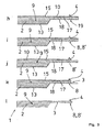
- FIG. 3 is in the FIGS. 3a to 3I the sequence of the inventive method for producing an SPM probe 1 according to the invention shown, in which the holding element 2, the spring bar 3 and the scanning tip 4 are made of monocrystalline silicon and the mark 8 is formed as a recess 8 'in the silicon.
- SPM probe 1 is assumed to start from a silicon wafer 9, which, like the FIG. 3a shows, on the front side 10 with a first etching masking layer 12 and on the back 11 is provided with a second ⁇ tzmask réelles slaughter 13.
- the etch-marking layer 12 on the front side 10 is structured by means of a photolithographic process in such a way that a locally limited masking 14 suitable for the generation of the scanning tip 4 remains.
- the FIG. 3b shows the silicon wafer 9 with the unchanged ⁇ tzmask réellestik 13 on the back 11 and the local masking 14 on the front side 10.
- the front side 10 of the silicon wafer 9 is etched away a bit, the masking 14 is undercut laterally, so that in the Figure 3c shown scanning tip 4 is formed.
- the silicon wafer 9 is thinned from the back 11 forth by means of an anisotropic deep etching in the region of the etching window 16 to the desired spring bar thickness, wherein the holding member 2 is machined out of the silicon wafer 9 with.
- 3f shows the silicon wafer 9 with the silicon membrane 17, from the later of the spring bar 3 is worked out. Then according to FIG. 3g an additional fourth ⁇ tzmasktechniks slaughter 18 introduced into the etching window 16, which there covers the silicon membrane 17 on the back side and the holding element 2 side.
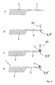
- FIG. 4 is in the FIGS. 4a to 4d the sequence of the inventive method for the preparation of in the FIG. 2 shown inventive SPM probe 1, in which the holding element 2 and the cantilever 3 are made of a first material, such as silicon, and the scanning tip 4 and 8 "designed as a mark 8 are formed by gas-induced material deposition by means of a focused particle beam.
- the first material or another second suitable material can be used for the scanning tip and the marking 8.
- the SPM probe 1 In the preparation of the SPM probe 1, one starts from an SPM probe 1 produced by a known method according to the FIG. 4a from, which has only one holding element 2 and a spring bar 3.
- the production of the scanning tip 4 on the underside 6 of the cantilever 3 and the raised mark 8 on the top 7 of the cantilever 3 is carried out by particle beam-induced material deposition, based on a gas-induced process.
- the particle beam 20, as in the Figures 4b, 4c shown directed to the bottom 6 of the cantilever 3 and focused.
- the focal plane and the beam power are selected such that a preferred local layer growth from the gas phase, such as FIG. 4b can be removed, induced by backscattered secondary particles induced on the top 7 of the cantilever 3 and so the mark 8 is formed as an increase 8 "first.
- the beam power and the beam energy is changed so that the material deposition, such as Figure 4c shows, preferably on the bottom 6 of the cantilever 3 by forward scattered secondary particles and thus the scanning tip 4 is constructed.
- the orientation of the particle beam 20 is not changed, so that the position of the marker 8 and the scanning tip 4 exactly at the in the FIG. 4d match finished SPM probe 1 shown.
Landscapes
- Physics & Mathematics (AREA)
- Health & Medical Sciences (AREA)
- General Health & Medical Sciences (AREA)
- General Physics & Mathematics (AREA)
- Nuclear Medicine, Radiotherapy & Molecular Imaging (AREA)
- Radiology & Medical Imaging (AREA)
- Length Measuring Devices With Unspecified Measuring Means (AREA)
Priority Applications (3)
| Application Number | Priority Date | Filing Date | Title |
|---|---|---|---|
| EP20080017867 EP2175286B1 (fr) | 2008-10-11 | 2008-10-11 | Procédé de fabrication d'une sonde SPM dotée d'une pointe de balayage et d'une aide à l'alignement installée à l'opposé de la pointe de balayage |
| US12/576,326 US8209768B2 (en) | 2008-10-11 | 2009-10-09 | Method of manufacturing an SPM probe with a scanning tip and with an alignment aid located opposite the scanning tip |
| JP2009236323A JP5032546B2 (ja) | 2008-10-11 | 2009-10-13 | 走査尖端部及びその裏面に位置合せ用目印を有する走査型微小センサの製造方法 |
Applications Claiming Priority (1)
| Application Number | Priority Date | Filing Date | Title |
|---|---|---|---|
| EP20080017867 EP2175286B1 (fr) | 2008-10-11 | 2008-10-11 | Procédé de fabrication d'une sonde SPM dotée d'une pointe de balayage et d'une aide à l'alignement installée à l'opposé de la pointe de balayage |
Publications (2)
| Publication Number | Publication Date |
|---|---|
| EP2175286A1 true EP2175286A1 (fr) | 2010-04-14 |
| EP2175286B1 EP2175286B1 (fr) | 2015-04-08 |
Family
ID=40394006
Family Applications (1)
| Application Number | Title | Priority Date | Filing Date |
|---|---|---|---|
| EP20080017867 Active EP2175286B1 (fr) | 2008-10-11 | 2008-10-11 | Procédé de fabrication d'une sonde SPM dotée d'une pointe de balayage et d'une aide à l'alignement installée à l'opposé de la pointe de balayage |
Country Status (3)
| Country | Link |
|---|---|
| US (1) | US8209768B2 (fr) |
| EP (1) | EP2175286B1 (fr) |
| JP (1) | JP5032546B2 (fr) |
Families Citing this family (2)
| Publication number | Priority date | Publication date | Assignee | Title |
|---|---|---|---|---|
| CN102474307B (zh) | 2010-04-12 | 2014-04-16 | 松下电器产业株式会社 | 阻抗稳定化装置 |
| TWI856828B (zh) * | 2023-09-23 | 2024-09-21 | 國立政治大學 | 影像掃描定位輔助系統 |
Citations (6)
| Publication number | Priority date | Publication date | Assignee | Title |
|---|---|---|---|---|
| EP0394962A2 (fr) | 1989-04-24 | 1990-10-31 | Olympus Optical Co., Ltd. | Microscope à forces atomiques |
| DE4126151A1 (de) * | 1990-08-31 | 1992-03-05 | Olympus Optical Co | Ausleger fuer ein scansondenmikroskop und ein verfahren zu dessen herstellung |
| JPH09204898A (ja) | 1996-01-24 | 1997-08-05 | Nikon Corp | カンチレバー及びそれを用いた粒子線アライメント支援機構 |
| JPH10123154A (ja) | 1996-10-18 | 1998-05-15 | Kagaku Gijutsu Shinko Jigyodan | 走査型プローブ顕微鏡用のプローブおよびその製造方法 |
| US5883387A (en) | 1994-11-15 | 1999-03-16 | Olympus Optical Co., Ltd. | SPM cantilever and a method for manufacturing the same |
| JP2003315238A (ja) | 2002-04-26 | 2003-11-06 | Jeol Ltd | 測定位置合わせ方法、カンチレバ及び走査形プローブ顕微鏡 |
Family Cites Families (5)
| Publication number | Priority date | Publication date | Assignee | Title |
|---|---|---|---|---|
| JPH03102209A (ja) * | 1989-09-16 | 1991-04-26 | Olympus Optical Co Ltd | 原子間力顕微鏡 |
| JPH07311207A (ja) * | 1994-03-23 | 1995-11-28 | Olympus Optical Co Ltd | Spmカンチレバー及びその製造方法 |
| JP4521482B2 (ja) * | 2004-04-26 | 2010-08-11 | オリンパス株式会社 | Spmカンチレバー及びその製造方法 |
| US7170048B2 (en) * | 2004-06-08 | 2007-01-30 | Olympus Corporation | Compound scanning probe microscope |
| US7808628B1 (en) * | 2005-03-08 | 2010-10-05 | California Institute Of Technology | Method for nanoscale spatial registration of scanning probes with substrates and surfaces |
-
2008
- 2008-10-11 EP EP20080017867 patent/EP2175286B1/fr active Active
-
2009
- 2009-10-09 US US12/576,326 patent/US8209768B2/en active Active
- 2009-10-13 JP JP2009236323A patent/JP5032546B2/ja active Active
Patent Citations (7)
| Publication number | Priority date | Publication date | Assignee | Title |
|---|---|---|---|---|
| EP0394962A2 (fr) | 1989-04-24 | 1990-10-31 | Olympus Optical Co., Ltd. | Microscope à forces atomiques |
| DE4126151A1 (de) * | 1990-08-31 | 1992-03-05 | Olympus Optical Co | Ausleger fuer ein scansondenmikroskop und ein verfahren zu dessen herstellung |
| DE4126151C2 (de) | 1990-08-31 | 2001-07-19 | Olympus Optical Co | Ausleger für ein Scansondenmikroskop und ein Verfahren zu dessen Herstellung |
| US5883387A (en) | 1994-11-15 | 1999-03-16 | Olympus Optical Co., Ltd. | SPM cantilever and a method for manufacturing the same |
| JPH09204898A (ja) | 1996-01-24 | 1997-08-05 | Nikon Corp | カンチレバー及びそれを用いた粒子線アライメント支援機構 |
| JPH10123154A (ja) | 1996-10-18 | 1998-05-15 | Kagaku Gijutsu Shinko Jigyodan | 走査型プローブ顕微鏡用のプローブおよびその製造方法 |
| JP2003315238A (ja) | 2002-04-26 | 2003-11-06 | Jeol Ltd | 測定位置合わせ方法、カンチレバ及び走査形プローブ顕微鏡 |
Non-Patent Citations (1)
| Title |
|---|
| GERHARD WAHRIG: "DEUTSCHES WÖRTERBUCH", 1997, BERTELSMANN LEXIKON VERLAG GMBH, GÜTERSLOH, ISBN: 3-577-10677-8, XP002526308 * |
Also Published As
| Publication number | Publication date |
|---|---|
| US8209768B2 (en) | 2012-06-26 |
| US20100095409A1 (en) | 2010-04-15 |
| JP5032546B2 (ja) | 2012-09-26 |
| EP2175286B1 (fr) | 2015-04-08 |
| JP2010091571A (ja) | 2010-04-22 |
Similar Documents
| Publication | Publication Date | Title |
|---|---|---|
| DE4126151C2 (de) | Ausleger für ein Scansondenmikroskop und ein Verfahren zu dessen Herstellung | |
| DE102016205941B4 (de) | Vorrichtung und Verfahren zum Analysieren eines Defekts einer fotolithographischen Maske oder eines Wafers | |
| DE69012555T2 (de) | Methode zur Herstellung von mikromechanischen Sensoren für AFM/STM/MFM-Profilometrie und mikromechanischer AFM/STM/MFM-Sensorkopf. | |
| DE69413373T2 (de) | Methode zur Herstellung von Faser-Tastspitzen unter Benutzung von strukturiertem reaktiven Ionenätzen | |
| DE102007052610A1 (de) | Nanosondenspitze für fortschrittliche Rastersondenmikroskopie mit einem Schichtsondenmaterial, das durch Lithographie und/oder durch lonenstrahltechniken strukturiert ist | |
| DE102011004214A1 (de) | Vorrichtung und Verfahren zum Analysieren und Verändern einer Probenoberfläche | |
| DE102019108116A1 (de) | Vorrichtung mit geladenem Partikelstrahl | |
| DE102014212563B4 (de) | Messvorrichtung und Verfahren zum Bestimmen einer Positionsänderung eines Teilchenstrahls eines Rasterteilchenmikroskops | |
| EP1359593B1 (fr) | Capteur pour la SPM et procedé pour sa fabrication | |
| EP2175286A1 (fr) | Sonde SPM dotée d'une aide à l'alignement installée à l'opposé de la pointe de balayage et son procédé de fabrication | |
| EP1113980B1 (fr) | Ouverture pratiquee dans un materiau semi-conducteur et realisation de cette ouverture et son utilisation | |
| DE60211672T2 (de) | Ionenstrahlerzeugungsvorrichtung | |
| EP2104111A1 (fr) | Sonde pour SPM avec un porte-à-faux raccourci | |
| DE4314301C1 (de) | Abtastvorrichtung zur Untersuchung von Oberflächenstrukturen mit Auflösung im submicron-Bereich und Verfahren zu deren Herstellung | |
| DE4445177C2 (de) | Verfahren zur Herstellung mikromechanischer Bauelemente mit freistehenden Mikrostrukturen | |
| DE69817452T2 (de) | Verfahren zur Herstellung einer micromechanischen Messsonde, insbesondere eines Rasterkraftmikroskops | |
| DE10303961B4 (de) | Sonde für ein optisches Nahfeldmikroskop und Verfahren zu deren Herstellung | |
| EP1359388B1 (fr) | Capteur du type SPM et son procédé de fabrication | |
| DE102007055540A1 (de) | Verfahren zum Korrigieren von Photomaskendefekten | |
| EP1347264B1 (fr) | Procédé de fabrication d'une sonde pour SPM | |
| DE19509903A1 (de) | Verfahren zur Herstellung einer Abtastvorrichtung zur kombinierten Untersuchung von verschiedenen Oberflächeneigenschaften mit Auflösung im Nanometerbereich | |
| DE19923444C2 (de) | Verfahren zur Herstellung einer lichttransparenten Sondenspitze | |
| EP1672648B1 (fr) | Sonde pour SPM avec une pointe deposée per EBD. | |
| DE69936221T2 (de) | Optischer ausleger für rastermikroskop und dessen herstellungsverfahren | |
| DE19926601B4 (de) | Apertur in einem Halbleitermaterial sowie Herstellung der Apertur und Verwendung |
Legal Events
| Date | Code | Title | Description |
|---|---|---|---|
| PUAI | Public reference made under article 153(3) epc to a published international application that has entered the european phase |
Free format text: ORIGINAL CODE: 0009012 |
|
| 17P | Request for examination filed |
Effective date: 20091006 |
|
| AK | Designated contracting states |
Kind code of ref document: A1 Designated state(s): AT BE BG CH CY CZ DE DK EE ES FI FR GB GR HR HU IE IS IT LI LT LU LV MC MT NL NO PL PT RO SE SI SK TR |
|
| AX | Request for extension of the european patent |
Extension state: AL BA MK RS |
|
| AKX | Designation fees paid |
Designated state(s): CH DE EE FR GB LI |
|
| 17Q | First examination report despatched |
Effective date: 20110217 |
|
| R17C | First examination report despatched (corrected) |
Effective date: 20110212 |
|
| GRAP | Despatch of communication of intention to grant a patent |
Free format text: ORIGINAL CODE: EPIDOSNIGR1 |
|
| INTG | Intention to grant announced |
Effective date: 20140915 |
|
| RIN1 | Information on inventor provided before grant (corrected) |
Inventor name: KRAUSE, OLIVER Inventor name: SULZBACH, THOMAS Inventor name: IRMER, BERND Inventor name: BURRI, MATHIEU Inventor name: DETTERBECK, MANFRED Inventor name: PENZKOFER, CHRISTIAN |
|
| GRAS | Grant fee paid |
Free format text: ORIGINAL CODE: EPIDOSNIGR3 |
|
| GRAP | Despatch of communication of intention to grant a patent |
Free format text: ORIGINAL CODE: EPIDOSNIGR1 |
|
| RIC1 | Information provided on ipc code assigned before grant |
Ipc: G01Q 70/16 20100101ALI20150130BHEP Ipc: G01Q 70/08 20100101AFI20150130BHEP |
|
| GRAA | (expected) grant |
Free format text: ORIGINAL CODE: 0009210 |
|
| INTG | Intention to grant announced |
Effective date: 20150216 |
|
| AK | Designated contracting states |
Kind code of ref document: B1 Designated state(s): CH DE EE FR GB LI |
|
| REG | Reference to a national code |
Ref country code: GB Ref legal event code: FG4D Free format text: NOT ENGLISH |
|
| REG | Reference to a national code |
Ref country code: CH Ref legal event code: EP |
|
| REG | Reference to a national code |
Ref country code: CH Ref legal event code: NV Representative=s name: ABACUS PATENTANWAELTE KLOCKE SPAETH BARTH, CH |
|
| REG | Reference to a national code |
Ref country code: DE Ref legal event code: R096 Ref document number: 502008012852 Country of ref document: DE Effective date: 20150521 |
|
| RIN2 | Information on inventor provided after grant (corrected) |
Inventor name: SULZBACH, THOMAS Inventor name: KRAUSE, OLIVER Inventor name: DETTERBECK, MANFRED Inventor name: IRMER, BERND Inventor name: PENZKOFER, CHRISTIAN Inventor name: BURRI, MATHIEU |
|
| REG | Reference to a national code |
Ref country code: FR Ref legal event code: PLFP Year of fee payment: 8 |
|
| REG | Reference to a national code |
Ref country code: DE Ref legal event code: R097 Ref document number: 502008012852 Country of ref document: DE |
|
| PG25 | Lapsed in a contracting state [announced via postgrant information from national office to epo] |
Ref country code: EE Free format text: LAPSE BECAUSE OF FAILURE TO SUBMIT A TRANSLATION OF THE DESCRIPTION OR TO PAY THE FEE WITHIN THE PRESCRIBED TIME-LIMIT Effective date: 20150408 |
|
| PLBE | No opposition filed within time limit |
Free format text: ORIGINAL CODE: 0009261 |
|
| STAA | Information on the status of an ep patent application or granted ep patent |
Free format text: STATUS: NO OPPOSITION FILED WITHIN TIME LIMIT |
|
| 26N | No opposition filed |
Effective date: 20160111 |
|
| REG | Reference to a national code |
Ref country code: FR Ref legal event code: PLFP Year of fee payment: 9 |
|
| REG | Reference to a national code |
Ref country code: FR Ref legal event code: PLFP Year of fee payment: 10 |
|
| REG | Reference to a national code |
Ref country code: FR Ref legal event code: PLFP Year of fee payment: 11 |
|
| REG | Reference to a national code |
Ref country code: DE Ref legal event code: R082 Ref document number: 502008012852 Country of ref document: DE Representative=s name: WITTE, WELLER & PARTNER PATENTANWAELTE MBB, DE |
|
| REG | Reference to a national code |
Ref country code: CH Ref legal event code: U11 Free format text: ST27 STATUS EVENT CODE: U-0-0-U10-U11 (AS PROVIDED BY THE NATIONAL OFFICE) Effective date: 20251101 |
|
| PGFP | Annual fee paid to national office [announced via postgrant information from national office to epo] |
Ref country code: DE Payment date: 20251028 Year of fee payment: 18 |
|
| PGFP | Annual fee paid to national office [announced via postgrant information from national office to epo] |
Ref country code: GB Payment date: 20251022 Year of fee payment: 18 |
|
| PGFP | Annual fee paid to national office [announced via postgrant information from national office to epo] |
Ref country code: FR Payment date: 20251029 Year of fee payment: 18 |
|
| PGFP | Annual fee paid to national office [announced via postgrant information from national office to epo] |
Ref country code: CH Payment date: 20251101 Year of fee payment: 18 |