EP2178121A1 - Verfahren zum Schutz und zur Dissipation von elektrostatischen Entladungen auf einen integrierten Schaltkreis - Google Patents
Verfahren zum Schutz und zur Dissipation von elektrostatischen Entladungen auf einen integrierten Schaltkreis Download PDFInfo
- Publication number
- EP2178121A1 EP2178121A1 EP09172773A EP09172773A EP2178121A1 EP 2178121 A1 EP2178121 A1 EP 2178121A1 EP 09172773 A EP09172773 A EP 09172773A EP 09172773 A EP09172773 A EP 09172773A EP 2178121 A1 EP2178121 A1 EP 2178121A1
- Authority
- EP
- European Patent Office
- Prior art keywords
- solid electrolyte
- electrode
- integrated circuit
- protection device
- electrically connected
- Prior art date
- Legal status (The legal status is an assumption and is not a legal conclusion. Google has not performed a legal analysis and makes no representation as to the accuracy of the status listed.)
- Withdrawn
Links
- 238000000034 method Methods 0.000 title claims abstract description 10
- 239000007784 solid electrolyte Substances 0.000 claims abstract description 93
- 229910052751 metal Inorganic materials 0.000 claims abstract description 90
- 239000002184 metal Substances 0.000 claims abstract description 90
- 229910021645 metal ion Inorganic materials 0.000 claims abstract description 36
- 150000004770 chalcogenides Chemical class 0.000 claims abstract description 7
- 239000000463 material Substances 0.000 claims description 48
- 150000002500 ions Chemical class 0.000 claims description 25
- 238000009792 diffusion process Methods 0.000 claims description 20
- 230000001681 protective effect Effects 0.000 claims description 16
- 230000004888 barrier function Effects 0.000 claims description 10
- PXHVJJICTQNCMI-UHFFFAOYSA-N Nickel Chemical compound [Ni] PXHVJJICTQNCMI-UHFFFAOYSA-N 0.000 claims description 8
- WFKWXMTUELFFGS-UHFFFAOYSA-N tungsten Chemical compound [W] WFKWXMTUELFFGS-UHFFFAOYSA-N 0.000 claims description 5
- 229910052721 tungsten Inorganic materials 0.000 claims description 5
- 239000010937 tungsten Substances 0.000 claims description 5
- RYGMFSIKBFXOCR-UHFFFAOYSA-N Copper Chemical compound [Cu] RYGMFSIKBFXOCR-UHFFFAOYSA-N 0.000 claims description 4
- 229910052802 copper Inorganic materials 0.000 claims description 4
- 239000010949 copper Substances 0.000 claims description 4
- 229910052759 nickel Inorganic materials 0.000 claims description 4
- 229910052709 silver Inorganic materials 0.000 claims description 3
- 239000004332 silver Substances 0.000 claims description 3
- 239000012777 electrically insulating material Substances 0.000 claims description 2
- 150000001455 metallic ions Chemical class 0.000 abstract 2
- 238000000151 deposition Methods 0.000 description 10
- 230000006378 damage Effects 0.000 description 9
- 230000008021 deposition Effects 0.000 description 6
- 239000003792 electrolyte Substances 0.000 description 6
- 239000000758 substrate Substances 0.000 description 6
- 238000005229 chemical vapour deposition Methods 0.000 description 5
- 239000004020 conductor Substances 0.000 description 5
- 239000002019 doping agent Substances 0.000 description 5
- -1 des ions Chemical class 0.000 description 4
- 238000010438 heat treatment Methods 0.000 description 4
- 230000005012 migration Effects 0.000 description 4
- 238000013508 migration Methods 0.000 description 4
- 239000004065 semiconductor Substances 0.000 description 4
- 238000011144 upstream manufacturing Methods 0.000 description 4
- 229910005866 GeSe Inorganic materials 0.000 description 3
- 230000015556 catabolic process Effects 0.000 description 3
- 230000003071 parasitic effect Effects 0.000 description 3
- 230000005855 radiation Effects 0.000 description 3
- 238000004544 sputter deposition Methods 0.000 description 3
- 241000861223 Issus Species 0.000 description 2
- FOIXSVOLVBLSDH-UHFFFAOYSA-N Silver ion Chemical compound [Ag+] FOIXSVOLVBLSDH-UHFFFAOYSA-N 0.000 description 2
- 230000008878 coupling Effects 0.000 description 2
- 238000010168 coupling process Methods 0.000 description 2
- 238000005859 coupling reaction Methods 0.000 description 2
- 239000006185 dispersion Substances 0.000 description 2
- 235000021183 entrée Nutrition 0.000 description 2
- 230000008020 evaporation Effects 0.000 description 2
- 238000001704 evaporation Methods 0.000 description 2
- 230000000670 limiting effect Effects 0.000 description 2
- 230000002269 spontaneous effect Effects 0.000 description 2
- 230000007704 transition Effects 0.000 description 2
- JBRZTFJDHDCESZ-UHFFFAOYSA-N AsGa Chemical compound [As]#[Ga] JBRZTFJDHDCESZ-UHFFFAOYSA-N 0.000 description 1
- 229910017214 AsGa Inorganic materials 0.000 description 1
- 229910004298 SiO 2 Inorganic materials 0.000 description 1
- XUIMIQQOPSSXEZ-UHFFFAOYSA-N Silicon Chemical compound [Si] XUIMIQQOPSSXEZ-UHFFFAOYSA-N 0.000 description 1
- ATJFFYVFTNAWJD-UHFFFAOYSA-N Tin Chemical compound [Sn] ATJFFYVFTNAWJD-UHFFFAOYSA-N 0.000 description 1
- 239000011149 active material Substances 0.000 description 1
- 230000001066 destructive effect Effects 0.000 description 1
- 239000003989 dielectric material Substances 0.000 description 1
- 238000007599 discharging Methods 0.000 description 1
- 238000004090 dissolution Methods 0.000 description 1
- 238000005530 etching Methods 0.000 description 1
- 229910052732 germanium Inorganic materials 0.000 description 1
- GNPVGFCGXDBREM-UHFFFAOYSA-N germanium atom Chemical compound [Ge] GNPVGFCGXDBREM-UHFFFAOYSA-N 0.000 description 1
- 238000004519 manufacturing process Methods 0.000 description 1
- 229910044991 metal oxide Inorganic materials 0.000 description 1
- 150000004706 metal oxides Chemical class 0.000 description 1
- 239000011368 organic material Substances 0.000 description 1
- 230000002093 peripheral effect Effects 0.000 description 1
- 238000000623 plasma-assisted chemical vapour deposition Methods 0.000 description 1
- 230000010287 polarization Effects 0.000 description 1
- 230000008569 process Effects 0.000 description 1
- 230000002829 reductive effect Effects 0.000 description 1
- 230000002441 reversible effect Effects 0.000 description 1
- 230000035945 sensitivity Effects 0.000 description 1
- 229910052710 silicon Inorganic materials 0.000 description 1
- 239000010703 silicon Substances 0.000 description 1
- 230000003068 static effect Effects 0.000 description 1
- 239000000126 substance Substances 0.000 description 1
- 229910052714 tellurium Inorganic materials 0.000 description 1
- PORWMNRCUJJQNO-UHFFFAOYSA-N tellurium atom Chemical compound [Te] PORWMNRCUJJQNO-UHFFFAOYSA-N 0.000 description 1
- 230000001960 triggered effect Effects 0.000 description 1
Images

Classifications
-
- H—ELECTRICITY
- H10—SEMICONDUCTOR DEVICES; ELECTRIC SOLID-STATE DEVICES NOT OTHERWISE PROVIDED FOR
- H10D—INORGANIC ELECTRIC SEMICONDUCTOR DEVICES
- H10D89/00—Aspects of integrated devices not covered by groups H10D84/00 - H10D88/00
- H10D89/60—Integrated devices comprising arrangements for electrical or thermal protection, e.g. protection circuits against electrostatic discharge [ESD]
-
- H—ELECTRICITY
- H10—SEMICONDUCTOR DEVICES; ELECTRIC SOLID-STATE DEVICES NOT OTHERWISE PROVIDED FOR
- H10N—ELECTRIC SOLID-STATE DEVICES NOT OTHERWISE PROVIDED FOR
- H10N70/00—Solid-state devices having no potential barriers, and specially adapted for rectifying, amplifying, oscillating or switching
Definitions
- the invention relates to the field of integrated circuits, and more particularly that of the protection of these integrated circuits against electrostatic discharges (ESD for "Electro Static Discharge”) may appear on connection lines of these integrated circuits.
- ESD Electrostatic Discharge
- MOS transistors Metal-Oxide Semiconductor
- ESD electrostatic discharge voltages
- the figure 1 represents an exemplary configuration in which an ESD protection device 10 is arranged between the inputs / outputs of an integrated circuit 16 comprising for example CMOS components, these inputs / outputs being represented by an input / output electrical line 12, and a ground 14.
- the ESD protection device 10 makes it possible to evacuate the electrostatic discharges or overvoltages appearing on the input / output electrical line 12 directly to the ground 14 without these discharges passing through the integrated circuit 16, protecting it as well as these surges.
- Such integrated ESD protection devices generally comprise an assembly of numerous components (diodes, MOS & bipolar transistors, resistors, etc.).
- the document US 7,242,558 B2 describes for example such an ESD protection device.
- this protection device Given the large number of components required for its implementation, this protection device is bulky, which is a major drawback when it must be integrated circuit that you want to protect.
- such an ESD protection device comprising a large number of components has the disadvantage of having a large parasitic capacitance limiting the bandwidth of the integrated circuit to be protected.
- this protection device operates only if the integrated circuit to be protected is live, given the need to supply at least the transistors of this device.
- An object of the present invention is to provide a protection device which is not bulky, requiring few components and / or having a less complex architecture than those of the devices of the prior art, making it possible to protect an integrated circuit when this it is powered on or off, and has a very low parasitic capacitance vis-à-vis the integrated circuit to protect.
- Such a protection device effectively protects an integrated circuit against electrostatic discharges and does not require peripheral polarization components.
- This protection device is also not bulky: typically, the diameter of the protection device may be equal to about 300 nm, and less than about 100 nm thick with respect to the ionizable metal portion and the solid electrolyte.
- Such a device allows for example to dissipate a current equal to about 10 mA for a period of time equal to about 1 second.
- This protection device also has a very low parasitic capacitance to the protected integrated circuit (for example less than about 100 fF), and therefore has a small impact on the operating bandwidth of the protected integrated circuit.
- the protective device when it is not subjected to an electrostatic discharge, it has a very high impedance (R> 10 9 ohms), thus not involving leakage currents or very low leakage currents.
- the protection device may further comprise a second electrode electrically connected to the ionizable metal portion.
- the portion of ionizable metal may be based on copper and / or silver, and / or the solid electrolyte may be based on a chalcogenide, and / or the electrode or electrodes may be based on nickel and / or tungsten.
- the thickness of the electrode or electrodes may be between about 100 nm and 300 nm, and / or the thickness of the solid electrolyte may be between about 10 nm and 100 nm, and / or the thickness of the portion ionizable metal may be between about 5 nm and 100 nm.
- the ionizable metal layer also performs the role of the electrode (the second electrode is in this case formed by the portion of ionizable metal itself), it may have a thickness less than about 500 nm, and for example equal to about 300 nm, or between about 300 nm and 500 nm.
- the protection device may furthermore comprise, when the material of the one or more electrodes is capable of diffusing ions in the solid electrolyte, a portion of ion diffusion preventing material, forming an ion diffusion barrier, arranged between the one or more electrodes and the solid electrolyte.
- the protection device may further comprise a portion of resistive material of conductivity lower than that of the material of the electrode or electrodes, disposed between the electrode and the ionizable metal portion, or between the electrodes. Such a portion of material makes it possible to limit the maximum current that can pass through the protection device.
- the protective device may further comprise, when the material of said portion of resistive material is capable of diffusing ions in the solid electrolyte, an ion diffusion barrier disposed between said portion of material and the solid electrolyte.
- the elements of the protection device may be surrounded by portions of electrically insulating material.
- the invention also relates to a method for protecting at least one integrated circuit against an electrostatic discharge, comprising at least the electrical connection of at least one protection device as described above, to an electrical input line and / or output of the integrated circuit, one of the electrode or the ionizable metal portion of the protection device being electrically connected to the input and / or output electrical line of the integrated circuit, the other being electrically connected to a mass.
- the electrode or the portion of ionizable metal electrically connected to ground may be connected directly to ground, or be connected to ground via at least one electronic device such as a filter, a power supply, a transformer or a coupler.
- the protection device comprises a second electrode electrically connected to the ionizable metal portion
- the ionizable metal portion may be electrically connected to the input and / or output electrical line of the integrated circuit or to ground via of the second electrode.
- the method may further comprise the connection and / or the electrical coupling of at least one second protection device as described above at the input and / or output electrical line of the integrated circuit, and wherein, when the ionizable metal portion of the first protection device is electrically connected to the input power line and / or output of the integrated circuit, the electrode of the second protection device can be electrically connected to the input and / or output electrical line of the integrated circuit and the ionizable metal portion of the second protection device can be connected electrically to the ground, and when the ionizable metal portion of the first protection device is electrically connected to ground, the ionizable metal portion of the second protection device can be electrically connected to the input and / or output electrical line of the integrated circuit and the electrode of the second protective device can be electrically connected to ground.
- the second protection device comprises a second electrode electrically connected to the ionizable metal portion of the second protection device
- the ionizable metal portion of the second protection device can be electrically connected to the input power line and / or output of the integrated circuit or ground through the second electrode.
- the resistivity of the assembly formed by the ionizable metal portion and the solid electrolyte can be lowered from an R HI value of greater than about 10 9 ohms to an R BI value of less than about 10. 3 ohms.
- the dissipation process may furthermore comprise, after the step of discharging the current resulting from the electrostatic discharge, a step of dispersing the metal ions having previously migrated into the solid electrolyte, which can increase the resistivity of the assembly formed by the ionizable metal portion and the solid electrolyte.
- the resistivity of the assembly formed by the ionizable metal portion and the solid electrolyte is increased from an R BI value of less than about 10 3 ohms to a higher R HI value. at about 10 9 ohms.
- FIG 2 represents a protection device 100 according to a first embodiment used for the protection of an integrated circuit against electrostatic discharges.
- This device 100 comprises a lower electrode 102 based on a conductive material, for example based on an inert metal such as tungsten and / or nickel, on which is disposed a solid electrolyte 104, for example based on chalcogenide , doped or not, such as GeSe, and / or GeS and / or WO x and / or based on tellurium.
- the lower electrode 102 has for example a thickness between about 100 nm and 300 nm.
- the solid electrolyte 104 has for example a thickness between about 10 nm and 100 nm.
- a diffusion barrier Ionic diffusion can be arranged between the lower electrode 102 and the solid electrolyte 104.
- Such an ion diffusion barrier is for example formed by a portion of Wn and / or TiN and / or any other material adapted to prevent a diffusion of ions in the solid electrolyte 104 from the lower electrode 102.
- the thickness of this ionic barrier is for example between about 10 nm and 20 nm.
- This metal is described as ionizable because when it is deposited on the solid electrolyte 104 or a step of thermal diffusion or radiation, this metal diffuses metal ions in the solid electrolyte 104.
- a diffusion barrier for example similar to that described above, can be arranged between the upper electrode 108 and the portion of ionizable metal 106.
- the solid electrolyte 104 comprises metal ions of a similar nature to the metal of the ionizable metal portion 106, originating from the ionizable metal portion 106. These metal ions have migrated since the portion of ionizable metal 106 in the solid electrolyte 104 during the deposition of the ionizable metal portion 106 on the solid electrolyte 104, and / or possibly after a subsequent diffusion step (for example by a heat treatment or by UV radiation ). In a variant, the metal ions can be integrated in the solid electrolyte 104 directly during the deposition of this solid electrolyte 104, for example by co-sputtering the solid electrolyte 104 and the ionizable metal 106.
- the concentration of metal ions in the solid electrolyte 104 is less than the metal ion saturation concentration of the solid electrolyte material 104 and is generally, for example, between about 5% and 50%.
- the value of the saturation concentration of metal ions in the solid electrolyte 104 is a function of the nature of the metal ions, as well as the nature of the solid electrolyte material. For example, in the case of a solid electrolyte 104 based on GeSe and an ionizable metal portion 106 based on Ag, the saturation concentration of silver ion in the solid electrolyte 104 is equal to about 30% . Thus, a silver ion concentration in the GeSe of less than about 30% will be chosen.
- the lower electrode 102, the assembly formed by the solid electrolyte 104 and the ionizable metal portion 106, and the upper electrode 108 are respectively surrounded by dielectric portions 110, 114 and 116 intended to thermally and electrically isolate the device. 100.
- These Dielectric portions are for example based on SiO 2 and / or Si 3 N 4 .
- Such a device 100 has small dimensions: for example, the total thickness of the solid electrolyte 104 and the ionizable metal portion 106 may be equal to about 65 nm, forming a protection device 100 of thickness equal to about 265 nm when the electrodes each have a thickness of about 100 nm.
- the diameter of the protection device 100 is for example equal to about 300 nm.
- the figure 3 represents the protection device 100 according to a second embodiment.
- the protection device 100 according to the second embodiment further comprises a portion of resistive material 112 disposed between the lower electrode 102 and the solid electrolyte 104.
- this portion of resistive material 112 could also be disposed between the upper electrode 108 and the ionizable metal portion 106.
- the resistive material of this portion 112 is chosen such that it has a lower conductivity than the material of the lower electrode 102 and / or the upper electrode 108, thus forming a series resistance inside the device 100 between the lower electrode 102 and the upper electrode 108, and making it possible to limit the current flowing through the device protection 100 between the electrodes 102 and 108 and thus to protect the device 100 from a eventual destruction if it was subjected to excessive ESD discharge.
- the dimensions of this portion of resistive material 112 are chosen as a function of the desired resistance and the resistivity of the material of this resistive portion 112.
- the maximum current that the protection device 100 can withstand is determined experimentally and the resistance intended to be presented by the protection device 100 is calculated from the value of this maximum current and the parameters related to the device to be protected, such as the maximum duration during which the device to be protected can be traversed by the current, or the maximum peak voltage tolerable by the device to be protected.
- the material of this resistive portion 112 may be chosen so that it does not diffuse ions in the solid electrolyte 104. In the case where the material of this portion 112 is capable of diffusing ions in the solid electrolyte 104, a diffusion barrier, for example similar to those previously described, may be disposed between this portion of resistive material 112 and the solid electrolyte 104.
- the device 100 has, between its two electrodes 102 and 108, a conductivity whose value is globally defined by the conductivity of the assembly formed by the solid electrolyte 104 and the ionizable metal portion 106, and possibly the resistive portion 112
- the conductivity of this assembly depends on the voltage applied across its terminals, that is to say on the voltage applied between the electrodes 102 and 108.
- the figure 4 graphically represents the variation of this conductivity (in ohms) as a function of the value of the voltage (in volts) applied between the electrodes 102 and 108.
- the device 100 has a first high impedance stable state R HI (with for example R HI > 10 9 ohms, or else 10 6 ⁇ R HI ⁇ 10 9 ohms), and a second low impedance state R BI (with for example R BI ⁇ 10 3 ohms, or else 10 ⁇ R BI ⁇ 10 3 ohms) triggered when the voltage between the electrodes 102, 108 exceeds a threshold voltage V thon , for example between about 500 mV and 5 V.
- V thon for example between about 500 mV and 5 V.
- V thon threshold voltage approaching as close as possible to the breakdown voltage limit of the materials used in the protection device 100.
- the return of the low impedance state R BI to the high impedance state R HI is done automatically when the value of the voltage between the electrodes 102, 108 goes back below one threshold V thoff , for example between about 2 00 mV and 2V, and of value less than the value of the threshold voltage V tuna .
- V thoff is lower than that of V tuna , forming a hysteresis dV th .
- the voltage across the electrodes 102 and 108 of the device 100 exceeds the threshold voltage V tuna .
- the metal ions in the solid electrolyte 104 then form a path of conduction in the electrolyte 104 by a migration phenomenon, causing the passage of the conductivity of the device 100 of the first high impedance state R HI to the second low impedance state R BI .
- the ESD discharge can thus be evacuated through the protective device 100.
- the voltage between the electrodes 102, 108 drops, going back to the V thoff threshold and causing the removal of the conduction path previously formed in the electrolyte 104 by the dispersion of the metal ions having previously migrated into the electrolyte 104.
- the protection device 100 then automatically returns to the high impedance stable state R HI .
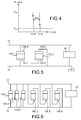
- the figure 5 represents an exemplary configuration in which an integrated circuit 16 is protected from electrostatic discharges.
- the integrated circuit 16 to be protected comprises an input and / or output line 12 and a line 14 connected to ground.
- a first protection device 100.1 as previously described according to the first or second embodiment is connected in parallel to the integrated circuit 16, between the input / output line 12 and the 14, upstream of the integrated circuit 16.
- a second protection device 100.2 is also connected in parallel to the integrated circuit 16, between the input / output line 12 and the ground 14, and also upstream of the integrated circuit 16.
- L upper electrode 108.1 of the first protection device 100.1 is electrically connected to the input / output line 12, the lower electrode 102.1 of the first protection device 100.1 being electrically connected to the ground 14.
- the upper electrode 108.2 of the second protection device 100.2 is electrically connected to the ground 14 and the lower electrode 102.2 of the second protection device 100.2 is electrically connected to the input / output line 12.
- each of the protection devices 100.1 and 100.2 has a unipolar operation (transition from the high impedance state R HI to the low impedance state R BI in the presence of a positive voltage between the lower electrode 102 and the upper electrode 108), this coupling makes it possible to provide a bipolar protection of the integrated circuit 16, protecting it from ESD discharges of indifferently positive or negative value appearing on the input / output line 12.
- the protection device will be connected as the first device 100.1 or as the second device 100.2 depending on the type of device. electrostatic discharges to be protected by the integrated circuit 16.
- the figure 6 represents an example of such a configuration in which six protection devices 100.1 to 100.6 are connected in parallel to the integrated circuit 16, between the input / output line 12 and the ground 14, upstream of the integrated circuit 16.
- the first three protection devices 100.1 to 100.3 comprise their upper electrodes connected to the input / output line 12 and their lower electrodes connected to ground 14, three second protection devices 100.4 to 100.6 comprising their electrodes.
- CMOS device 16 a bipolar protection of the CMOS device 16 is obtained by six protection devices 100, thus making it possible to withstand high electrostatic discharge currents, the discharge current being evenly distributed between three of the protection devices 100 according to the e sign of electrostatic surge.
- figure 6 can be generalized: an integrated circuit 16 can be protected by N protection devices 100, with N strictly positive integer. Moreover, in the case of a bipolar protection, part of the N protection devices can be connected in reverse to the integrated circuit 16 with respect to the other protection devices, in a manner analogous to the configuration previously described in connection with the figure 6 . In addition, the number of protective devices inversely connected between the input / output line and the ground is not necessarily equal to the number of non-inverted protective devices connected between the input / output line and the ground. the mass.
- the lower electrode 102 is first made by depositing a layer of conductive material for forming this lower electrode 102, for example by sputtering, CVD (Chemical Vapor Deposition), PECVD (Chemical Vapor Deposition) assisted by plasma), evaporation or any other suitable deposition technique, on a semiconductor substrate, for example based on silicon, germanium, or AsGa, or of the SOI type, not shown.
- This substrate may also be based on an organic material, the substrate being in this case electrically insulating. It is also possible that this conductive material is deposited on a metal layer itself disposed on the substrate and intended to form an electrical connection with other elements made on the substrate and / or the connection lines of the integrated circuit or circuits to be protected.
- the layer of conductive material deposited is then etched to form the lower electrode 102 according to the desired size and shape.
- the dimensions of the section of the lower electrode 102 which is to be traversed by the currents of the electrostatic discharges will be chosen as a function of the value of the maximum current intended to pass through the protection device 100.
- This lower electrode may for example have sides of dimensions equal to about 1 micron, and a thickness of about 300 nm.
- the dielectric portions 114 are then formed around the lower electrode 102 by deposition of a dielectric material and planarization with a stop on the lower electrode 102.
- a layer of resistive material is then deposited on the lower electrode 102 and on the dielectric portions 114, and then etched to form the resistive portion 112. In the case of the first embodiment, these steps of producing the resistive portion 112 are omitted.
- a layer of material intended to form the solid electrolyte 104 is then deposited on the resistive portion 112 or on the lower electrode 102, as well as on the dielectric portions.
- a layer of the ionizable metal for example based on copper and / or tungsten, intended for forming the ionizable metal portion 106 is then deposited on the solid electrolyte material layer 104.
- Metal ions from the ionizable metal layer 106 diffuse into the layer of chalcogenide material to form the solid electrolyte 104 during the deposition of the ionizable metal 106 on the solid electrolyte layer 104.
- These layers are then etched according to the dimensions desired to form the solid electrolyte 104 and the ionizable metal portion 106. If some of the materials used (except the active material 106) are capable of diffusing ions in the solid electrolyte 104, it is possible to implement steps for producing diffusion barriers between the electrolyte 104 and these materials, for example by depositing layers of suitable materials between the electrodes in question and the solid electrolyte 104 and engraving them to the desired dimensions.
- solid electrolyte 104 it is also possible to implement a step of doping the solid electrolyte 104, for example when this material is not intrinsically doped, for example by a thermal diffusion of dopants from a layer of dopants previously deposited on the substrate. solid electrolyte 104 and whose dopants self-diffuse during deposition, or by UV insolation or additional heat treatment.
- an additional diffusion step which may consist of a heat treatment or UV radiation produced on the ionizable metal portion 106 and the solid electrolyte 104.
- Dielectric portions 110 are then made by deposition and planarization around the elements 112, 104 and 106. Finally, the upper electrode 108 and the dielectric portions 116 are made, for example in a similar manner to the lower electrode 102 and the portions dielectric 114.
- the materials used to produce the various elements of the protection device 100 may be deposited by sputtering, CVD (chemical vapor deposition), evaporation or any other suitable deposition technique, and etching and / or planarization for example mechanical-chemical (CMP).
- CVD chemical vapor deposition
- evaporation evaporation or any other suitable deposition technique
- CMP mechanical-chemical
- the thickness of the ionizable metal portion 106 is determined as a function of the material of the electrodes 102, 108, of the type of dissolution in the electrolyte (spontaneous diffusion and / or diffusion stimulated by UV doping or heat treatment of the ionizable metal). ), the desired switching voltage V thon and the thickness of the solid electrolyte 104.
- the thickness of the ionizable metal portion 106 may for example be between about 5 nm and 100 nm.
- the concentration of metal ions from the ionizable metal portion 106 in the solid electrolyte 104 can be adjusted to achieve the desired switching voltage.
- This switching voltage is preferably chosen to be less than a saturation voltage to guarantee a return to the high spontaneous impedance state. This adjustment can be obtained by choosing an adequate thickness of the ionizable metal portion 106, this optimum thickness being able to be determined by different experimental tests.
- the lower electrode 102 and the upper electrode 108 have dimensions greater than those of the elements 112, 104 and 106 in a plane (x, y) (along the x, y and z axes represented on the Figures 2 and 3 ).
- the surface of the active zone of the protection device 100 (this surface corresponding to that which a current traverses during the dissipation of electrostatic discharges) is defined by the surface of the solid electrolyte 104 in the (x, y) plane. ), this surface being similar to the surface of the ionizable metal portion 106 in this same plane. This surface is for example between about 700 nm 2 to 0.07 micrometers 2 .
Landscapes
- Semiconductor Integrated Circuits (AREA)
Applications Claiming Priority (1)
| Application Number | Priority Date | Filing Date | Title |
|---|---|---|---|
| FR0857033A FR2937462B1 (fr) | 2008-10-16 | 2008-10-16 | Procede de protection et de dissipation de decharges electrostatiques sur un circuit integre |
Publications (1)
| Publication Number | Publication Date |
|---|---|
| EP2178121A1 true EP2178121A1 (de) | 2010-04-21 |
Family
ID=40577892
Family Applications (1)
| Application Number | Title | Priority Date | Filing Date |
|---|---|---|---|
| EP09172773A Withdrawn EP2178121A1 (de) | 2008-10-16 | 2009-10-12 | Verfahren zum Schutz und zur Dissipation von elektrostatischen Entladungen auf einen integrierten Schaltkreis |
Country Status (4)
| Country | Link |
|---|---|
| US (1) | US20100097735A1 (de) |
| EP (1) | EP2178121A1 (de) |
| JP (1) | JP2010098316A (de) |
| FR (1) | FR2937462B1 (de) |
Families Citing this family (5)
| Publication number | Priority date | Publication date | Assignee | Title |
|---|---|---|---|---|
| FR2934711B1 (fr) * | 2008-07-29 | 2011-03-11 | Commissariat Energie Atomique | Dispositif memoire et memoire cbram a fiablilite amelioree. |
| JP5544621B2 (ja) * | 2010-09-22 | 2014-07-09 | 独立行政法人物質・材料研究機構 | 電気化学トランジスタ |
| JPWO2013103122A1 (ja) * | 2012-01-05 | 2015-05-11 | 日本電気株式会社 | スイッチング素子及びその製造方法 |
| WO2013146986A1 (ja) | 2012-03-29 | 2013-10-03 | 宇部興産株式会社 | 水性ポリウレタン樹脂分散体 |
| US9019769B2 (en) * | 2012-12-11 | 2015-04-28 | Macronix International Co., Ltd. | Semiconductor device and manufacturing method and operating method for the same |
Citations (6)
| Publication number | Priority date | Publication date | Assignee | Title |
|---|---|---|---|---|
| US3343085A (en) * | 1966-09-20 | 1967-09-19 | Energy Conversion Devices Inc | Overvoltage protection of a.c. measuring devices |
| EP0261938A2 (de) * | 1986-09-26 | 1988-03-30 | Raychem Limited | Schaltungsschutzeinrichtung |
| US7164566B2 (en) | 2004-03-19 | 2007-01-16 | Freescale Semiconductor, Inc. | Electrostatic discharge protection device and method therefore |
| US7242558B2 (en) | 2004-06-01 | 2007-07-10 | Taiwan Semiconductor Co., Ltd. | ESD protection module triggered by BJT punch-through |
| US20070200155A1 (en) * | 2006-02-28 | 2007-08-30 | Infineon Technologies Ag | Method of fabricating an integrated electronic circuit with programmable resistance cells |
| EP1873758A2 (de) * | 2006-06-27 | 2008-01-02 | Hitachi Global Storage Technologies Netherlands B.V. | Magnetoresistiver Sensor mit Struktur zur Aktivierung und Deaktivierung einer Schaltung zur Vermeidung elektrostatischer Entladung |
Family Cites Families (1)
| Publication number | Priority date | Publication date | Assignee | Title |
|---|---|---|---|---|
| US7751163B2 (en) * | 2006-09-29 | 2010-07-06 | Qimonda Ag | Electric device protection circuit and method for protecting an electric device |
-
2008
- 2008-10-16 FR FR0857033A patent/FR2937462B1/fr not_active Expired - Fee Related
-
2009
- 2009-09-01 US US12/551,853 patent/US20100097735A1/en not_active Abandoned
- 2009-10-12 EP EP09172773A patent/EP2178121A1/de not_active Withdrawn
- 2009-10-15 JP JP2009238271A patent/JP2010098316A/ja active Pending
Patent Citations (6)
| Publication number | Priority date | Publication date | Assignee | Title |
|---|---|---|---|---|
| US3343085A (en) * | 1966-09-20 | 1967-09-19 | Energy Conversion Devices Inc | Overvoltage protection of a.c. measuring devices |
| EP0261938A2 (de) * | 1986-09-26 | 1988-03-30 | Raychem Limited | Schaltungsschutzeinrichtung |
| US7164566B2 (en) | 2004-03-19 | 2007-01-16 | Freescale Semiconductor, Inc. | Electrostatic discharge protection device and method therefore |
| US7242558B2 (en) | 2004-06-01 | 2007-07-10 | Taiwan Semiconductor Co., Ltd. | ESD protection module triggered by BJT punch-through |
| US20070200155A1 (en) * | 2006-02-28 | 2007-08-30 | Infineon Technologies Ag | Method of fabricating an integrated electronic circuit with programmable resistance cells |
| EP1873758A2 (de) * | 2006-06-27 | 2008-01-02 | Hitachi Global Storage Technologies Netherlands B.V. | Magnetoresistiver Sensor mit Struktur zur Aktivierung und Deaktivierung einer Schaltung zur Vermeidung elektrostatischer Entladung |
Non-Patent Citations (1)
| Title |
|---|
| KOZICKI M N ET AL: "Mass transport in chalcogenide electrolyte films - materials and applications", JOURNAL OF NON-CRYSTALLINE SOLIDS, NORTH-HOLLAND PHYSICS PUBLISHING. AMSTERDAM, NL, vol. 352, no. 6-7, 15 May 2006 (2006-05-15), pages 567 - 577, XP025187128, ISSN: 0022-3093, [retrieved on 20060515] * |
Also Published As
| Publication number | Publication date |
|---|---|
| JP2010098316A (ja) | 2010-04-30 |
| FR2937462B1 (fr) | 2010-12-24 |
| US20100097735A1 (en) | 2010-04-22 |
| FR2937462A1 (fr) | 2010-04-23 |
Similar Documents
| Publication | Publication Date | Title |
|---|---|---|
| WO2011089179A1 (fr) | Dispositif electronique, en particulier de protection contre les décharges électrostatistiques, et procédé de protection d'un composant contre des décharges électrostatiques | |
| EP2178121A1 (de) | Verfahren zum Schutz und zur Dissipation von elektrostatischen Entladungen auf einen integrierten Schaltkreis | |
| EP3577683A1 (de) | Struktur für funkfrequenzanwendungen | |
| EP2290691A1 (de) | Schutzvorrichtung für einen integrierten Schaltkreis gegen elektrostatische Entladungen | |
| FR2691839A1 (fr) | Capteur à Effet Hall. | |
| EP0200599A1 (de) | Verfahren zur Herstellung von nichtlinearen Steuerelementen für elektrooptische Anzeigeschirmplatte und eine nach diesem Verfahren hergestellte Schirmplatte | |
| FR3030115A1 (fr) | Condensateur a capacite variable comprenant une couche de materiau a changement d'etat et un procede de variation d'une capacite d'un condensateur | |
| FR2513032A1 (fr) | Dispositif de protection integre contre les surtensions d'un circuit electronique, et circuit electronique protege par ce dispositif | |
| EP0664564A1 (de) | Integrierte Schaltung, die ein Schutzanordnung gegen elektrostatische Entladungen enthält | |
| EP0202150A1 (de) | Nichtlineares Steuerelement für elektrooptische Anzeigeschirmplatte und Verfahren zu dessen Herstellung | |
| EP3712908B1 (de) | Schutzvorrichtung gegen überspannungen | |
| EP0624943B1 (de) | Seriengeschaltetes Strombegrenzerbauelement | |
| FR2934713A1 (fr) | Substrat de type semi-conducteur sur isolant a couches de diamant intrinseque et dope | |
| EP1147559A1 (de) | Schutzbauteil gegen elektrostatische entladungen für mikroelektronische komponenten auf soi-substrat | |
| EP0554195B1 (de) | Selbsttätig geschütztes Halbleiterschutzelement | |
| FR2794898A1 (fr) | Dispositif semi-conducteur a tension de seuil compensee et procede de fabrication | |
| EP1400887A1 (de) | Schutzgerät für einen elektronischen Chip, der vertaulichen Informationen enthält | |
| EP2685497A1 (de) | Integrierter SOI-Schaltkreis, der eine seitliche Diode zum Schutz gegen elektrostatische Entladungen umfasst | |
| EP3942577B1 (de) | Überspannungsschutz | |
| FR3066310A1 (fr) | Cellule memoire de type ram resistive | |
| FR2766984A1 (fr) | Dispositif de protection d'une charge electrique et circuit d'alimentation comportant un tel dispositif | |
| EP0269475A1 (de) | Schutz einer elektropyrotechnischen Vorrichtung gegen elektrostatische Entladungen | |
| EP4142451B1 (de) | Verfahren zur herstellung von resistiven speicherzellen | |
| EP2648335B1 (de) | Hyperfrequenz-Leistungsbegrenzer mit kapazitiven Funkfrequenz-MEMS-Schaltern | |
| WO2023148196A1 (fr) | Transistor non-volatil à effet de champ à base de gaz bidimensionnel d'électrons |
Legal Events
| Date | Code | Title | Description |
|---|---|---|---|
| PUAI | Public reference made under article 153(3) epc to a published international application that has entered the european phase |
Free format text: ORIGINAL CODE: 0009012 |
|
| AK | Designated contracting states |
Kind code of ref document: A1 Designated state(s): AT BE BG CH CY CZ DE DK EE ES FI FR GB GR HR HU IE IS IT LI LT LU LV MC MK MT NL NO PL PT RO SE SI SK SM TR |
|
| AX | Request for extension of the european patent |
Extension state: AL BA RS |
|
| RAP1 | Party data changed (applicant data changed or rights of an application transferred) |
Owner name: COMMISSARIAT A L'ENERGIE ATOMIQUE ET AUX ENERGIES |
|
| 17P | Request for examination filed |
Effective date: 20101015 |
|
| STAA | Information on the status of an ep patent application or granted ep patent |
Free format text: STATUS: THE APPLICATION IS DEEMED TO BE WITHDRAWN |
|
| 18D | Application deemed to be withdrawn |
Effective date: 20120503 |