EP2180504B1 - Herstellungsverfahren einer Halbeiteranordnung - Google Patents
Herstellungsverfahren einer Halbeiteranordnung Download PDFInfo
- Publication number
- EP2180504B1 EP2180504B1 EP20100153752 EP10153752A EP2180504B1 EP 2180504 B1 EP2180504 B1 EP 2180504B1 EP 20100153752 EP20100153752 EP 20100153752 EP 10153752 A EP10153752 A EP 10153752A EP 2180504 B1 EP2180504 B1 EP 2180504B1
- Authority
- EP
- European Patent Office
- Prior art keywords
- layer
- sidewall spacer
- region
- forming
- semiconductor body
- Prior art date
- Legal status (The legal status is an assumption and is not a legal conclusion. Google has not performed a legal analysis and makes no representation as to the accuracy of the status listed.)
- Ceased
Links
Images




Classifications
-
- H—ELECTRICITY
- H10—SEMICONDUCTOR DEVICES; ELECTRIC SOLID-STATE DEVICES NOT OTHERWISE PROVIDED FOR
- H10D—INORGANIC ELECTRIC SEMICONDUCTOR DEVICES
- H10D30/00—Field-effect transistors [FET]
- H10D30/60—Insulated-gate field-effect transistors [IGFET]
- H10D30/791—Arrangements for exerting mechanical stress on the crystal lattice of the channel regions
- H10D30/797—Arrangements for exerting mechanical stress on the crystal lattice of the channel regions being in source or drain regions, e.g. SiGe source or drain
-
- H—ELECTRICITY
- H10—SEMICONDUCTOR DEVICES; ELECTRIC SOLID-STATE DEVICES NOT OTHERWISE PROVIDED FOR
- H10D—INORGANIC ELECTRIC SEMICONDUCTOR DEVICES
- H10D30/00—Field-effect transistors [FET]
- H10D30/01—Manufacture or treatment
- H10D30/021—Manufacture or treatment of FETs having insulated gates [IGFET]
-
- H—ELECTRICITY
- H10—SEMICONDUCTOR DEVICES; ELECTRIC SOLID-STATE DEVICES NOT OTHERWISE PROVIDED FOR
- H10D—INORGANIC ELECTRIC SEMICONDUCTOR DEVICES
- H10D30/00—Field-effect transistors [FET]
- H10D30/60—Insulated-gate field-effect transistors [IGFET]
- H10D30/601—Insulated-gate field-effect transistors [IGFET] having lightly-doped drain or source extensions, e.g. LDD IGFETs or DDD IGFETs
- H10D30/608—Insulated-gate field-effect transistors [IGFET] having lightly-doped drain or source extensions, e.g. LDD IGFETs or DDD IGFETs having non-planar bodies, e.g. having recessed gate electrodes
-
- H—ELECTRICITY
- H10—SEMICONDUCTOR DEVICES; ELECTRIC SOLID-STATE DEVICES NOT OTHERWISE PROVIDED FOR
- H10D—INORGANIC ELECTRIC SEMICONDUCTOR DEVICES
- H10D62/00—Semiconductor bodies, or regions thereof, of devices having potential barriers
- H10D62/01—Manufacture or treatment
- H10D62/021—Forming source or drain recesses by etching e.g. recessing by etching and then refilling
-
- H—ELECTRICITY
- H10—SEMICONDUCTOR DEVICES; ELECTRIC SOLID-STATE DEVICES NOT OTHERWISE PROVIDED FOR
- H10D—INORGANIC ELECTRIC SEMICONDUCTOR DEVICES
- H10D64/00—Electrodes of devices having potential barriers
- H10D64/01—Manufacture or treatment
- H10D64/015—Manufacture or treatment removing at least parts of gate spacers, e.g. disposable spacers
-
- H—ELECTRICITY
- H10—SEMICONDUCTOR DEVICES; ELECTRIC SOLID-STATE DEVICES NOT OTHERWISE PROVIDED FOR
- H10D—INORGANIC ELECTRIC SEMICONDUCTOR DEVICES
- H10D84/00—Integrated devices formed in or on semiconductor substrates that comprise only semiconducting layers, e.g. on Si wafers or on GaAs-on-Si wafers
- H10D84/01—Manufacture or treatment
- H10D84/0123—Integrating together multiple components covered by H10D12/00 or H10D30/00, e.g. integrating multiple IGBTs
- H10D84/0126—Integrating together multiple components covered by H10D12/00 or H10D30/00, e.g. integrating multiple IGBTs the components including insulated gates, e.g. IGFETs
- H10D84/0165—Integrating together multiple components covered by H10D12/00 or H10D30/00, e.g. integrating multiple IGBTs the components including insulated gates, e.g. IGFETs the components including complementary IGFETs, e.g. CMOS devices
- H10D84/0167—Manufacturing their channels
-
- H—ELECTRICITY
- H10—SEMICONDUCTOR DEVICES; ELECTRIC SOLID-STATE DEVICES NOT OTHERWISE PROVIDED FOR
- H10D—INORGANIC ELECTRIC SEMICONDUCTOR DEVICES
- H10D84/00—Integrated devices formed in or on semiconductor substrates that comprise only semiconducting layers, e.g. on Si wafers or on GaAs-on-Si wafers
- H10D84/01—Manufacture or treatment
- H10D84/0123—Integrating together multiple components covered by H10D12/00 or H10D30/00, e.g. integrating multiple IGBTs
- H10D84/0126—Integrating together multiple components covered by H10D12/00 or H10D30/00, e.g. integrating multiple IGBTs the components including insulated gates, e.g. IGFETs
- H10D84/0165—Integrating together multiple components covered by H10D12/00 or H10D30/00, e.g. integrating multiple IGBTs the components including insulated gates, e.g. IGFETs the components including complementary IGFETs, e.g. CMOS devices
- H10D84/017—Manufacturing their source or drain regions, e.g. silicided source or drain regions
-
- H—ELECTRICITY
- H10—SEMICONDUCTOR DEVICES; ELECTRIC SOLID-STATE DEVICES NOT OTHERWISE PROVIDED FOR
- H10D—INORGANIC ELECTRIC SEMICONDUCTOR DEVICES
- H10D84/00—Integrated devices formed in or on semiconductor substrates that comprise only semiconducting layers, e.g. on Si wafers or on GaAs-on-Si wafers
- H10D84/01—Manufacture or treatment
- H10D84/0123—Integrating together multiple components covered by H10D12/00 or H10D30/00, e.g. integrating multiple IGBTs
- H10D84/0126—Integrating together multiple components covered by H10D12/00 or H10D30/00, e.g. integrating multiple IGBTs the components including insulated gates, e.g. IGFETs
- H10D84/0165—Integrating together multiple components covered by H10D12/00 or H10D30/00, e.g. integrating multiple IGBTs the components including insulated gates, e.g. IGFETs the components including complementary IGFETs, e.g. CMOS devices
- H10D84/0184—Manufacturing their gate sidewall spacers
-
- H—ELECTRICITY
- H10—SEMICONDUCTOR DEVICES; ELECTRIC SOLID-STATE DEVICES NOT OTHERWISE PROVIDED FOR
- H10D—INORGANIC ELECTRIC SEMICONDUCTOR DEVICES
- H10D84/00—Integrated devices formed in or on semiconductor substrates that comprise only semiconducting layers, e.g. on Si wafers or on GaAs-on-Si wafers
- H10D84/01—Manufacture or treatment
- H10D84/02—Manufacture or treatment characterised by using material-based technologies
- H10D84/03—Manufacture or treatment characterised by using material-based technologies using Group IV technology, e.g. silicon technology or silicon-carbide [SiC] technology
- H10D84/038—Manufacture or treatment characterised by using material-based technologies using Group IV technology, e.g. silicon technology or silicon-carbide [SiC] technology using silicon technology, e.g. SiGe
-
- H—ELECTRICITY
- H10—SEMICONDUCTOR DEVICES; ELECTRIC SOLID-STATE DEVICES NOT OTHERWISE PROVIDED FOR
- H10D—INORGANIC ELECTRIC SEMICONDUCTOR DEVICES
- H10D84/00—Integrated devices formed in or on semiconductor substrates that comprise only semiconducting layers, e.g. on Si wafers or on GaAs-on-Si wafers
- H10D84/80—Integrated devices formed in or on semiconductor substrates that comprise only semiconducting layers, e.g. on Si wafers or on GaAs-on-Si wafers characterised by the integration of at least one component covered by groups H10D12/00 or H10D30/00, e.g. integration of IGFETs
- H10D84/82—Integrated devices formed in or on semiconductor substrates that comprise only semiconducting layers, e.g. on Si wafers or on GaAs-on-Si wafers characterised by the integration of at least one component covered by groups H10D12/00 or H10D30/00, e.g. integration of IGFETs of only field-effect components
- H10D84/83—Integrated devices formed in or on semiconductor substrates that comprise only semiconducting layers, e.g. on Si wafers or on GaAs-on-Si wafers characterised by the integration of at least one component covered by groups H10D12/00 or H10D30/00, e.g. integration of IGFETs of only field-effect components of only insulated-gate FETs [IGFET]
-
- H—ELECTRICITY
- H10—SEMICONDUCTOR DEVICES; ELECTRIC SOLID-STATE DEVICES NOT OTHERWISE PROVIDED FOR
- H10D—INORGANIC ELECTRIC SEMICONDUCTOR DEVICES
- H10D86/00—Integrated devices formed in or on insulating or conducting substrates, e.g. formed in silicon-on-insulator [SOI] substrates or on stainless steel or glass substrates
- H10D86/201—Integrated devices formed in or on insulating or conducting substrates, e.g. formed in silicon-on-insulator [SOI] substrates or on stainless steel or glass substrates the substrates comprising an insulating layer on a semiconductor body, e.g. SOI
Definitions
- This invention relates to a method of fabricating a semiconductor device.
- Semiconductor devices are used in a large number of electronic devices such as computers, cell phones and others.
- One of the goals of the semiconductor industry is to continue shrinking the size and increasing the speed of individual devices. Smaller devices can operate at higher speeds since the physical distance between components is smaller.
- higher conductivity materials such as copper are replacing lower conductivity materials such as aluminum.
- One other challenge is to increase the mobility of semiconductor carriers such as electrons and holes.
- One technique to improve transistor performance is to mechanically strain (i.e., distort) the semiconductor crystal lattice near the charge-carrier channel region.
- Transistors built on strained silicon for example, have greater charge-carrier mobility than those fabricated using conventional substrates.
- One way to create strain is to provide a stress layer over the transistor.
- Variants of stress layers can be used for mobility and performance boost of devices.
- stress can be provided by a contact etch stop layer (CESL), single layers, dual layers, stress memory transfer layers, and STI liners.
- CTL contact etch stop layer
- Most of these techniques use nitride layers to provide tensile or compressive stresses; however, other materials can be used in other applications, e.g., HDP oxide layers.
- Another technique to strain silicon is to provide a layer of germanium or silicon germanium.
- a thin layer of silicon may be grown over the germanium-containing layer. Since the germanium crystal lattice constant is larger than the silicon lattice constant, the germanium-containing layer creates a lattice mismatch stress in adjacent layers. Due to the different lattice structures, the SiGe will impart a strain onto the silicon layer. This strained silicon layer can be utilized to fabricate faster transistors.
- a strained-silicon CMOS device with a shallow trench isolation (STI) oxide region is disclosed in U.S. Patent Application Publication No. 2005/0101077 , which is incorporated herein by reference.
- a silicon substrate is formed and a relaxed-SiGe layer is formed over the silicon substrate or a SiGe-on-insulator substrate with a buried oxide (BOX) layer.
- a strained-Si layer overlies the relaxed-SiGe layer.
- a silicon oxide layer is formed over the strained-Si layer and a silicon nitride hardmask layer is formed over the silicon oxide layer.
- the silicon nitride layer, the silicon oxide layer, the strained-Si layer, and the relaxed-SiGe layer are etched to form an STI trench.
- a sacrificial oxide liner is formed on the STI trench surface to round and reduce stress at the STI trench corners. The sacrificial oxide liner is then removed and the STI trench is filled with silicon oxide.
- a substrate includes a first semiconductor material with a first natural lattice constant, a gate dielectric layer on the substrate, a gate electrode on the gate dielectric layer, a source region and drain region oppositely adjacent to the gate dielectric layer, and a spacer on a sidewall of the gate electrode.
- One or both of the source region and drain region are recessed to form a recess.
- the recess can then be filled with a second semiconductor material with a second natural lattice constant different from the first natural lattice constant as a lattice-mismatched zone.
- Document US 6,417,056 B1 relates to a method to form a low overlap capacitance transistor by forming a micro trench at the gate edge.
- Document US 2002/0135015 A1 relates to a method for forming a self-aligned local-halo semiconductor device.
- Document US 2005/0035369 A1 relates to a method of forming an integrated circuit utilizing a strained channel transistor.
- Document US 2004/0021179 A1 relates to a method for fabricating a transistor having a drain punch through blocking region.
- Document US 6,403,482 B1 relates to a self aligned junction isolation.
- trenches are etched next to transistor gates. These trenches are filled with epitaxial SiGe or other material that has a different lattice constant than silicon. Due to the different lattice constants or thermal expansion coefficients, mechanical stress is produced and issued onto the transistor channel, resulting in improved carrier mobilities and thus improved transistor performance.
- Examples are provided that expand upon these concepts by etching trenches of identical lengths at well defined positions in the vicinity of a transistor gate.
- trenches are etched with different lengths caused by the non-constant pattern density in different areas of a circuit. Trenches of different lengths or depths cause different mechanical stress. Therefore, an equal impact of the mechanical stress on the transistor performance is not guaranteed for all transistors. This results in different transistor parameters depending upon the position and environment of a transistor in a circuit, as well as on the distance to neighboring transistor gates.
- a self-aligned etching and filling of grooves or recesses in silicon (or another semiconductor) in the neighborhood of a gate in the neighborhood of a gate.
- the method assures a uniform length of the trenches resulting in a uniform filling with equivalent amounts of material.
- One advantage is that the trenches can be designed uniformly over the wafer surface. This allows for good stress optimization.
- a gate electrode is formed over a semiconductor body (e.g., bulk silicon substrate or SOI layer).
- the gate electrode is electrically insulated from the semiconductor body.
- a first sidewall spacer is formed along a sidewall of the gate electrode.
- a masking layer is formed over the semiconductor body including the gate electrode and the first sidewall spacer.
- a sacrificial sidewall spacer is formed over the masking layer adjacent the first sidewall spacer.
- a planarization layer is formed over the semiconductor body such that a portion of the planarization layer is adjacent the sacrificial sidewall spacer. The sacrificial sidewall spacer is then removed and a recess etched in the semiconductor body.
- the recess is aligned between the masking layer over the first sidewall spacer and the portion of the planarization layer. Thereafter, a semiconductor material (e.g., SiGe or SiC) is formed in the recess using the masking layer as a deposition mask.
- a semiconductor material e.g., SiGe or SiC
- a transistor in a first embodiment, includes an isolation region (e.g., STI) and a gate electrode disposed over an upper surface of the semiconductor body.
- a sidewall spacer is disposed along a sidewall of the gate electrode.
- a region of a second semiconductor material is embedded within the semiconductor body. The region of second semiconductor material is located adjacent the sidewall spacer.
- a first gate electrode is disposed over an upper surface of the semiconductor body and a first sidewall spacer is disposed along a sidewall of the first gate electrode.
- a second gate electrode is also disposed over an upper surface of the semiconductor body and a second sidewall spacer is disposed along a sidewall of the second gate electrode.
- Figure 1 is a cross-sectional view of a first example of transistor structure
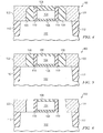
- Figures 2-10 provide cross-sectional views illustrating a first example of a process for producing a transistor structure
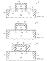
- Figures 11-18 provide cross-sectional views illustrating an embodiment process for producing a structure of the present invention
- Figure 19 is a cross-sectional view of an example.
- Figure 20 is a cross-sectional view of an alternate example.
- the present invention will be described with respect to preferred embodiments in a specific context, namely a transistor device with a strained channel.
- the invention may also be applied, however, to other structures that require strained or stressed semiconductor regions or other structures that require one material to be embedded in a region of another material.
- Figure 1 illustrates a first examplary structure 100 that is formed in a semiconductor body 102.
- the semiconductor body 102 can be a bulk semiconductor substrate, a region (e.g., well or tub) within a substrate, or a semiconductor layer over a substrate.
- the present invention works well with semiconductor-on-insulator (SOI) technology.
- SOI semiconductor-on-insulator
- the semiconductor body is made of silicon. In other embodiments, other materials can be used.
- isolation region 112 is a trench isolation (e.g., shallow trench isolation or STI) region that surrounds the active area.
- the STI region 112 can be formed, for example, by forming a trench that is filled with a dielectric such as silicon oxide or a silicon nitride.
- One purpose of the isolation region 112 is to electrically isolate structures 100 in the active region from surrounding structures. In other examples, the isolation could be created by deep trench isolation, mesa isolation, or field isolation, as but three examples.
- the active region contains a transistor 100.
- Transistor 100 includes a gate electrode 104 that is disposed over an upper surface of the semiconductor body 102.
- the gate electrode 104 can be formed from one or more conductors such as polysilicon or a metal, or a combination of both.
- the gate electrode 104 includes a silicide (e.g., nickel silicide, tungsten silicide, titanium silicide) overlying a polysilicon region.
- the metal gate can be a metal (e.g., Ir, Ru, RuTa, Ti, Mo), metal silicide (e.g., a fully silicided gate), metal nitride (e.g., HfN, TiN, TaSiN) or other.
- metal e.g., Ir, Ru, RuTa, Ti, Mo
- metal silicide e.g., a fully silicided gate
- metal nitride e.g., HfN, TiN, TaSiN
- the gate electrode 104 is electrically insulated from a channel region 118 by a gate dielectric 106.
- the gate dielectric can be an oxide, a nitride or a combination of oxide and nitride (e.g., silicon oxynitride (SiON) or an oxide-nitride-oxide (ONO) stack), for example.
- the gate dielectric 106 can be a high-k dielectric (i.e., a dielectric with a dielectric constant greater than the dielectric constant of Si 3 N 4 ). Examples of high-k dielectrics that can be used as a gate dielectric include HfO 2 (nitrided) Hf silicate, Al 2 O 3, ZrO 2 Zr-Al-O, and Zr silicate.
- a hard mask layer 108 overlies the gate electrode 104.
- the hard mask layer 108 is typically formed from an insulating material, such as silicon nitride. This layer is typically formed as part of the fabrication process of the gate electrode and can be eliminated if desired.
- a sidewall spacer 110 is disposed along a sidewall of the gate electrode 104 and, in this example, hard mask layer 108.
- the sidewall spacer 110 includes multiple layers such as a nitride and an oxide.
- the sidewall spacer 110 can be a single oxide region or a single nitride region. In yet other examples, other materials can be used.
- the transistor 100 also includes source/drain regions 114. During operation, current will flow between the source/drain regions 114 depending upon a voltage applied to the gate electrode 104.
- the present invention applies equally to n-channel transistors (e.g., where the source/drain regions 114 are doped with n-type impurities and the channel 118 is doped with p-type impurities) and p-channel transistors (e.g., where the source/drain regions 114 are doped with p-type impurities and the channel 118 is doped with n-type impurities).
- the invention also applies to both depletion mode and enhancement mode transistors.
- a silicide region (not shown) can be included over the source/drain regions 114.
- the source/drain regions 114 each further include a region of a second semiconductor material 116 embedded within the semiconductor body 102.
- the semiconductor material 116 is a different material than the material of semiconductor body 102. For example, by using a material with a different lattice constant a strained channel 118 can be formed. This strained channel will enhance the mobility of carriers during operation thus creating a faster transistor.
- the semiconductor body 102 is made from silicon and the second semiconductor material 116 is silicon germanium (SiGe). Silicon germanium has a larger natural lattice constant than silicon and will therefore create a compressive channel stress. This situation is ideal for p-channel transistors.
- the second semiconductor material is silicon carbon (SiC), which has a natural lattice constant that is smaller than that of silicon. In that case, a tensile channel stress will be created, which speeds up the electron carriers in an n-channel transistor.
- the n-channel transistor and the p-channel transistor of a CMOS implementation are formed using different materials.
- the different conductivity-type transistors can each include an embedded region 116 with a different material (e.g., SiGe for the p-channel and SiC for the n-channel).
- transistors of one type e.g., p-channel
- transistors of the other type e.g., n-channel
- all transistors both n-channel and p-channel are identical.
- the embedded semiconductor material 116 extends above the upper surface of the semiconductor body 102. This feature is not required.
- the semiconductor material 116 can be substantially planar with the semiconductor body 102 or could be recessed below the upper surface of the semiconductor body 102. In one example, which is not illustrated, the embedded material 116 is recessed below the upper surface and covered with a layer of silicon, which can be planar with the remaining silicon body.
- the embedded material 116 extends from the gate stack 104 by a distance that is independent of the length of the source/drain 114. It has been discovered that the length of the embedded material 116 influences the amount of strain placed on channel 118. When the length is constant, the strain can be more easily controlled even when the spacing between transistors is not constant. In other words, the stress variations between dense and isolated transistors will be small. As a result, in this example, the region of second semiconductor material 116 is adjacent the sidewall spacer 110 but laterally spaced from the isolation region 112. Since the length of the embedded material region 116 is constant, the amount by which the material 116 is laterally spaced from the isolation region 112 will be a function of the distance between the isolation region 112 and the gate electrode 104 (or sidewall spacer 110).
- a transistor has been partially fabricated.
- STI regions 112 and a gate stack which includes gate dielectric 106, gate electrode 104, and hard mask layer 108, have been formed using conventional processes.
- Sidewall spacers 110 have also been formed along sidewalls of the gate electrode 104. These spacers can be formed by conformally depositing an insulating material and anisotropically etching the material. The thickness of the spacer can be determined by the desired dimension of the source/drain extension (or lightly doped source/drain region), which is not explicitly illustrated.
- sacrificial sidewall spacers 120 are formed adjacent the sidewall spacers 110. These spacers 120 can be formed by conformally depositing the spacer material and anisotropically etching the material.
- the spacer material which can be either an insulator or a conductor, is selected such that it can be selectively removed with respect to the sidewall spacer 110 and hard mask layer 108.
- the sacrificial spacer is formed using low temperature oxide (LTO) process. This thickness of the spacer is determined by the desired length of the embedded semiconductor region (116 in Figure 1 ).
- LTO low temperature oxide
- the sacrificial spacer has a length of between about 30 nm and 100 nm along the surface of the semiconductor body 102.
- the gate electrode 104 has a length of between about 30 nm and 100 nm. Consequently, the ratio of the sacrificial spacer length to the gate length is between about 1:2 and 2:1.
- the length of the sacrificial spacer along the surface of the body 102 will define the length of the embedded semiconductor region 116.
- a planarization layer 122 can then be formed over the structure as shown in Figure 4 .
- the planarization layer material is selected such that sacrificial spacer 120 can be removed selectively with respect to the layer 122.
- the planarization layer 122 is formed by depositing and reflowing a layer of borophosphosilicate glass (BPSG). In other examples, other materials can be used.
- BPSG borophosphosilicate glass
- an upper surface of the wafer is removed.
- This process can be performed with a chemical-mechanical polish (CMP) or a reactive ion etch (RIE).
- CMP chemical-mechanical polish
- RIE reactive ion etch
- the resulting structure is planar. In other embodiments (see Figure 14 , for example), this result is not required.
- portions of the sacrificial spacer 120 will be exposed.
- the sacrificial spacer 120 is removed selective to the sidewall spacers 110 and the planarization layer 122.
- an isotropic wet etch is performed.
- the sacrificial spacer 120 is made from a low temperature oxide
- the sidewall spacer 110 (or at least the exposed portions of the sidewall spacer 110) is made from a nitride
- the planarization layer is made from BPSG. With these materials, the sacrificial oxide can be removed.
- recesses 124 are etched into regions of the semiconductor body 102 that are exposed by the removal of the sacrificial spacer.
- the recess can be etched to a depth between about 20 nm and about 150 nm.
- a recess of a depth of about 30 nm to about 45 nm can be used in an SOI example and a recess of about 100 nm can be etched for a bulk example.
- the length of the recess will correspond to the length of the sacrificial spacer 120 and the width of the recess (i.e., the distance into and out of the page in Figure 7 ) will correspond to the transistor width (or active area width).
- the embedded semiconductor regions 116 can then be formed as illustrated in Figure 8 .
- SiGe or SiC is selectively deposited using an epitaxial growth process. This semiconductor can be doped in situ or deposited undoped.
- silicon germanium is doped in situ with boron to create a p-channel transistor. If the n-channel transistors are to include regions embedded with a different material, they can be masked (e.g., with photoresist) at this point. If the n-channel transistors include no embedded region, they would be masked during the step of forming the recess as well.
- silicon carbon is deposited and doped in situ with arsenic or phosphorus.
- source/drain dopants 126 can be implanted, as shown in Figure 10 .
- the source/drain dopants 126 can be boron and for n-channel transistors, the source/drain dopants 126 can be arsenic or phosphorus, for example.
- a process for fabricating a transistor is illustrated with respect to Figures 11-16 . Due to the similarity with the process of the first example, many of the details will not be repeated. It is understood that either process can be varied using any of the details discussed herein.
- Figure 11 illustrates a structure that is similar to the structure of Figure 2 but additionally includes a masking layer 128.
- Masking layer 128 is included to protect the gate stack and sidewall spacers 110 during the removal of the sacrificial sidewall spacer 120.
- the masking layer 128 is a silicon nitride (e.g., Si 3 N 4 ) with a thickness of about 10 to about 50 nm.
- the sidewall spacer 110 and the sacrificial spacer 120 can be formed from the same material.
- the formation of the sacrificial spacer 120 is shown in Figure 12 and the formation of planarization layer 122 is shown in Figure 13 .
- the materials of sacrificial spacer 120 and planarization layer 122 be selected so that the spacer 120 can be selectively removed.
- the planarization layer 122 is formed from a resist while the sacrificial spacer is formed from an oxide.
- the resist material can be spun on in a substantially planar manner.
- the choice of sacrificial spacer material is independent of the material of sidewall spacer 110.
- the planarization material is then etched back as shown in Figure 14 .
- the amount of etch back should be sufficient to expose a portion of the sacrificial spacer 120 but still leave enough material 122 to protect semiconductor body 102 during the subsequent recess etch.
- the thickness of the resist layer can be 500-1000 nm before the recess, and 50-100nm after the recess.
- the sacrificial spacer can then be selectively removed as shown in Figure 15 .
- This removal can be done by wet etch using diluted or buffered HF in the case of an oxide sacrificial spacer, or alternatively by dry etching.
- This step will expose a portion of the masking layer 128 over the semiconductor body 102.
- This exposed portion of the masking layer can then be opened, for example, using an anisotropic etch process.
- Figure 16 illustrates the recess etch that was described earlier with respect to Figure 7 .
- the resist 122 is removed as shown in Figure 17 and the trenches are filled as described in the earlier example.
- the selective deposition of semiconductor material 116 is illustrated in Figure 18 , where the layer 128 is used as a mask for the selective deposition. The layer 128 can then be removed or allowed to remain.
- FIGs 19 and 20 illustrate two examples that can utilize concepts of the present invention.
- two transistors 100a and 100b are shown. Both transistors are formed in the same semiconductor body 102 but have different dimensions. Shallow trench isolation regions 112 are shown but it is understood that other isolation techniques (e.g., mesa isolation for SOI devices) could be utilized. It is also understood that these two transistors are shown next to each to simplify illustration. The transistors could be spaced from one another anywhere on the die and could have source/drain current paths that are oriented at different angles from each other.
- both transistors 100a and 100b include embedded semiconductor regions 116 of the same length (i.e., the distance extending in parallel with the current path).
- the width of the embedded regions would be the same as the transistor's channel width and may vary from transistor to transistor.
- the region 116a has a length L that is the same as the length L of the region 116b. This is true even though the distance between sidewall spacer 1 10a and isolation region 112 is smaller than the distance between sidewall spacer 110b and isolation region 112. Since the embedded regions 116a and 116b have similar dimensions, it is more likely that they will apply similar stresses to their associated channel regions.
- Figure 20 illustrates another example where two transistors 100a and 100b are formed in a single active region.
- the embedded region 116a-r is spaced from the embedded region 116b-1 without any intervening isolation regions. This situation can occur, for example, when two transistors have a shared source/drain region. Despite the shared source/drain, each transistor 100a and 100b has a separate set of embedded regions 116 of the same length.
- the embedded regions 116a and 116b can include the same or different semiconductor materials.
- transistor 100a is an n-channel transistor and transistor 100b is a p-channel transistor
- the region 116a can be embedded with SiC while the region 116 is embedded with SiGe.
- a silicide region or other conductor (not shown) can be used to electrically couple across the common source/drain region.
Landscapes
- Insulated Gate Type Field-Effect Transistor (AREA)
- Thin Film Transistor (AREA)
- Metal-Oxide And Bipolar Metal-Oxide Semiconductor Integrated Circuits (AREA)
Claims (7)
- Verfahren zum Herstellen einer Halbleitervorrichtung (100), wobei das Verfahren umfasst:Ausbilden einer Gate-Elektrode (104) über einem Halbleiterkörper (102), wobei die Gate-Elektrode (104) elektrisch vom Halbleiterkörper (102) isoliert ist;Ausbilden eines ersten Seitenwand-Abstandshalters (110) entlang einer Seitenwand der Gate-Elektrode (104);Ausbilden einer Maskierungsschicht (128) über dem Halbleiterkörper (102), eingeschlossen über der Gateelektrode (104) unddem ersten Seitenwand-Abstandshalter (110);Ausbilden eines Opfer-Seitenwand-Abstandshalters (120) über der Maskierungsschicht (128) angrenzend an den ersten Seitenwand-Abstandshalter (110), wobei der Opfer-Seitenwand-Abstandshalter (120) und der erste Seitenwand-Abstandshalter (110) über dem Halbleiterkörper (102) liegen;Ausbilden einer Planarisierungsschicht (122) über dem Halbleiterkörper (102) derart, dass ein Abschnitt der Planarisierungsschicht (122) an den Opfer-Seitenwand-Abstandshalter (120) angrenzt;Entfernen des Opfer-Seitenwand-Abstandshalters (120);Ätzen einer Aussparung (124) in den Halbleiterkörper (102), wobei die Aussparung (124) zwischen der Maskierungsschicht über dem ersten Seitenwand-Abstandshalter (110) und dem Abschnitt der Planarisierungsschicht (122) ausgerichtet ist;Entfernen der Planarisierungsschicht (122); undanschließendes Ausbilden eines Halbleitermaterials (116) in der Aussparung (124) unter Verwendung der Maskierungsschicht (128) als eine Ablagerungsmaske.
- Verfahren nach Anspruch 1, wobei das Ausbilden der Planarisierungsschicht (122) das Ausbilden einer Resistschicht aufweist.
- Verfahren nach Anspruch 2, wobei das Ausbilden der Planarisierungsschicht (122) ferner ein Rückätzen der Resistschicht aufweist.
- Verfahren nach Anspruch 3, wobei das Ausbilden der Resistschicht (122) ein Aufspinnen einer Resistschicht aufweist.
- Verfahren nach Anspruch 1, wobei die Maskierungsschicht (128) eine Siliziumnitridschicht aufweist.
- Verfahren nach Anspruch 1, wobei das Ausbilden der Planarisierungsschicht (122) ein Abscheiden eines Materials, das Sauerstoff umfasst, und ein Durchführen eines chemischmechanischen Polierprozesses aufweist.
- Verfahren nach Anspruch 1, wobei der Halbleiterkörper (102) Silizium umfasst und das Halbleitermaterial eines aus SiGe oder SiC umfasst.
Priority Applications (1)
| Application Number | Priority Date | Filing Date | Title |
|---|---|---|---|
| EP14150531.3A EP2720256B1 (de) | 2005-09-13 | 2006-09-13 | Verspannte Halbleiteranordnung |
Applications Claiming Priority (2)
| Application Number | Priority Date | Filing Date | Title |
|---|---|---|---|
| US11/224,825 US8003470B2 (en) | 2005-09-13 | 2005-09-13 | Strained semiconductor device and method of making the same |
| EP20060120572 EP1763073B1 (de) | 2005-09-13 | 2006-09-13 | Verspannte Halbleiteranordnung |
Related Parent Applications (2)
| Application Number | Title | Priority Date | Filing Date |
|---|---|---|---|
| EP06120572.0 Division | 2006-09-13 | ||
| EP20060120572 Division EP1763073B1 (de) | 2005-09-13 | 2006-09-13 | Verspannte Halbleiteranordnung |
Related Child Applications (2)
| Application Number | Title | Priority Date | Filing Date |
|---|---|---|---|
| EP14150531.3A Division EP2720256B1 (de) | 2005-09-13 | 2006-09-13 | Verspannte Halbleiteranordnung |
| EP14150531.3A Division-Into EP2720256B1 (de) | 2005-09-13 | 2006-09-13 | Verspannte Halbleiteranordnung |
Publications (3)
| Publication Number | Publication Date |
|---|---|
| EP2180504A2 EP2180504A2 (de) | 2010-04-28 |
| EP2180504A3 EP2180504A3 (de) | 2013-03-13 |
| EP2180504B1 true EP2180504B1 (de) | 2015-03-25 |
Family
ID=37487523
Family Applications (3)
| Application Number | Title | Priority Date | Filing Date |
|---|---|---|---|
| EP20060120572 Ceased EP1763073B1 (de) | 2005-09-13 | 2006-09-13 | Verspannte Halbleiteranordnung |
| EP14150531.3A Not-in-force EP2720256B1 (de) | 2005-09-13 | 2006-09-13 | Verspannte Halbleiteranordnung |
| EP20100153752 Ceased EP2180504B1 (de) | 2005-09-13 | 2006-09-13 | Herstellungsverfahren einer Halbeiteranordnung |
Family Applications Before (2)
| Application Number | Title | Priority Date | Filing Date |
|---|---|---|---|
| EP20060120572 Ceased EP1763073B1 (de) | 2005-09-13 | 2006-09-13 | Verspannte Halbleiteranordnung |
| EP14150531.3A Not-in-force EP2720256B1 (de) | 2005-09-13 | 2006-09-13 | Verspannte Halbleiteranordnung |
Country Status (4)
| Country | Link |
|---|---|
| US (4) | US8003470B2 (de) |
| EP (3) | EP1763073B1 (de) |
| JP (1) | JP4644173B2 (de) |
| CN (1) | CN1945854B (de) |
Families Citing this family (50)
| Publication number | Priority date | Publication date | Assignee | Title |
|---|---|---|---|---|
| US7402207B1 (en) | 2004-05-05 | 2008-07-22 | Advanced Micro Devices, Inc. | Method and apparatus for controlling the thickness of a selective epitaxial growth layer |
| US7402485B1 (en) | 2004-10-20 | 2008-07-22 | Advanced Micro Devices, Inc. | Method of forming a semiconductor device |
| US7456062B1 (en) | 2004-10-20 | 2008-11-25 | Advanced Micro Devices, Inc. | Method of forming a semiconductor device |
| US7553732B1 (en) | 2005-06-13 | 2009-06-30 | Advanced Micro Devices, Inc. | Integration scheme for constrained SEG growth on poly during raised S/D processing |
| US20060281271A1 (en) * | 2005-06-13 | 2006-12-14 | Advanced Micro Devices, Inc. | Method of forming a semiconductor device having an epitaxial layer and device thereof |
| US7572705B1 (en) | 2005-09-21 | 2009-08-11 | Advanced Micro Devices, Inc. | Semiconductor device and method of manufacturing a semiconductor device |
| US7696019B2 (en) * | 2006-03-09 | 2010-04-13 | Infineon Technologies Ag | Semiconductor devices and methods of manufacturing thereof |
| JP2007243105A (ja) * | 2006-03-13 | 2007-09-20 | Sony Corp | 半導体装置およびその製造方法 |
| DE102006015075A1 (de) * | 2006-03-31 | 2007-10-11 | Advanced Micro Devices, Inc., Sunnyvale | Technik zur Bereitstellung von Verspannungsquellen in MOS-Transistoren in unmittelbarer Nähe zu einem Kanalgebiet |
| US7763517B2 (en) * | 2007-02-12 | 2010-07-27 | Macronix International Co., Ltd. | Method of forming non-volatile memory cell |
| JP5286701B2 (ja) * | 2007-06-27 | 2013-09-11 | ソニー株式会社 | 半導体装置および半導体装置の製造方法 |
| US9640666B2 (en) * | 2007-07-23 | 2017-05-02 | GlobalFoundries, Inc. | Integrated circuit employing variable thickness film |
| US7652336B2 (en) * | 2007-08-06 | 2010-01-26 | International Business Machines Corporation | Semiconductor devices and methods of manufacture thereof |
| JP5389346B2 (ja) * | 2007-10-11 | 2014-01-15 | 富士通セミコンダクター株式会社 | Mos電界効果トランジスタおよびその製造方法 |
| US7923365B2 (en) * | 2007-10-17 | 2011-04-12 | Samsung Electronics Co., Ltd. | Methods of forming field effect transistors having stress-inducing sidewall insulating spacers thereon |
| JP5107680B2 (ja) * | 2007-11-16 | 2012-12-26 | パナソニック株式会社 | 半導体装置 |
| US7786518B2 (en) * | 2007-12-27 | 2010-08-31 | Texas Instruments Incorporated | Growth of unfaceted SiGe in MOS transistor fabrication |
| US8293631B2 (en) | 2008-03-13 | 2012-10-23 | International Business Machines Corporation | Semiconductor devices having tensile and/or compressive stress and methods of manufacturing |
| US7892932B2 (en) * | 2008-03-25 | 2011-02-22 | International Business Machines Corporation | Semiconductor devices having tensile and/or compressive strain and methods of manufacturing and design structure |
| US7772095B2 (en) * | 2008-05-28 | 2010-08-10 | International Business Machines Corporation | Integrated circuit having localized embedded SiGe and method of manufacturing |
| KR101399099B1 (ko) * | 2008-06-02 | 2014-05-26 | 삼성전자주식회사 | 콘택 구조체를 포함하는 반도체 소자 및 그 형성 방법 |
| KR101035614B1 (ko) * | 2008-10-23 | 2011-05-19 | 주식회사 동부하이텍 | 플래시 메모리 소자의 제조방법 |
| US8106456B2 (en) * | 2009-07-29 | 2012-01-31 | International Business Machines Corporation | SOI transistors having an embedded extension region to improve extension resistance and channel strain characteristics |
| JP5434360B2 (ja) | 2009-08-20 | 2014-03-05 | ソニー株式会社 | 半導体装置及びその製造方法 |
| US20110049582A1 (en) * | 2009-09-03 | 2011-03-03 | International Business Machines Corporation | Asymmetric source and drain stressor regions |
| KR101674179B1 (ko) * | 2010-04-06 | 2016-11-10 | 삼성전자주식회사 | 전계 효과 트랜지스터를 포함하는 반도체 소자 및 그 형성 방법 |
| CN102214574B (zh) * | 2010-04-07 | 2013-06-12 | 中国科学院微电子研究所 | 一种半导体器件的制造方法 |
| CN102314927B (zh) * | 2010-07-06 | 2014-02-05 | 中国科学院物理研究所 | 一种磁性随机存储单元阵列、存储器及其读写方法 |
| US8361859B2 (en) * | 2010-11-09 | 2013-01-29 | International Business Machines Corporation | Stressed transistor with improved metastability |
| US8941182B2 (en) * | 2011-06-07 | 2015-01-27 | Globalfoundries Inc. | Buried sublevel metallizations for improved transistor density |
| US8697557B2 (en) * | 2011-06-07 | 2014-04-15 | Globalfoundries Inc. | Method of removing gate cap materials while protecting active area |
| US8921944B2 (en) * | 2011-07-19 | 2014-12-30 | United Microelectronics Corp. | Semiconductor device |
| CN102903638B (zh) * | 2011-07-29 | 2016-03-30 | 中国科学院微电子研究所 | 半导体器件及其制造方法 |
| FR2985089B1 (fr) * | 2011-12-27 | 2015-12-04 | Commissariat Energie Atomique | Transistor et procede de fabrication d'un transistor |
| CN103367151B (zh) * | 2012-03-30 | 2015-12-16 | 中国科学院微电子研究所 | 使源/漏区更接近沟道区的mos器件及其制作方法 |
| US8841190B2 (en) | 2012-03-30 | 2014-09-23 | The Institute of Microelectronics Chinese Academy of Science | MOS device for making the source/drain region closer to the channel region and method of manufacturing the same |
| US8866230B2 (en) * | 2012-04-26 | 2014-10-21 | United Microelectronics Corp. | Semiconductor devices |
| CN103632973B (zh) * | 2012-08-23 | 2017-01-25 | 中国科学院微电子研究所 | 半导体器件及其制造方法 |
| US9419126B2 (en) * | 2013-03-15 | 2016-08-16 | GlobalFoundries, Inc. | Integrated circuits and methods for fabricating integrated circuits with active area protection |
| CN104103586B (zh) * | 2013-04-10 | 2017-03-22 | 中芯国际集成电路制造(上海)有限公司 | 半导体器件的形成方法 |
| CN104143512B (zh) * | 2013-05-09 | 2017-02-22 | 中芯国际集成电路制造(上海)有限公司 | Pmos晶体管的制作方法 |
| CN104517822B (zh) * | 2013-09-27 | 2017-06-16 | 中芯国际集成电路制造(北京)有限公司 | 一种半导体器件的制造方法 |
| US9379214B2 (en) * | 2014-02-14 | 2016-06-28 | Semi Solutions Llc | Reduced variation MOSFET using a drain-extension-last process |
| US10123723B2 (en) | 2014-03-10 | 2018-11-13 | InnerSpace Neuro Solutions, Inc. | Air line protection coupling for a catheter |
| US9941388B2 (en) * | 2014-06-19 | 2018-04-10 | Globalfoundries Inc. | Method and structure for protecting gates during epitaxial growth |
| TWI555120B (zh) * | 2014-10-14 | 2016-10-21 | 力晶科技股份有限公司 | 半導體元件及其製作方法 |
| US10008582B2 (en) * | 2016-11-28 | 2018-06-26 | Globalfoundries Inc. | Spacers for tight gate pitches in field effect transistors |
| CN109473429B (zh) * | 2018-10-26 | 2021-08-03 | 中国科学院微电子研究所 | 半导体器件及其制造方法及包括其的电子设备 |
| US11289375B2 (en) | 2020-03-23 | 2022-03-29 | International Business Machines Corporation | Fully aligned interconnects with selective area deposition |
| CN116799005B (zh) * | 2023-08-22 | 2023-11-28 | 合肥晶合集成电路股份有限公司 | 一种半导体结构及其制备方法 |
Citations (1)
| Publication number | Priority date | Publication date | Assignee | Title |
|---|---|---|---|---|
| US6403482B1 (en) * | 2000-06-28 | 2002-06-11 | International Business Machines Corporation | Self-aligned junction isolation |
Family Cites Families (50)
| Publication number | Priority date | Publication date | Assignee | Title |
|---|---|---|---|---|
| JPH03272182A (ja) | 1990-03-22 | 1991-12-03 | Matsushita Electron Corp | 半導体装置の製造方法 |
| JPH0479337A (ja) | 1990-07-23 | 1992-03-12 | Oki Electric Ind Co Ltd | 半導体素子およびその製造方法 |
| US5364497A (en) * | 1993-08-04 | 1994-11-15 | Analog Devices, Inc. | Method for fabricating microstructures using temporary bridges |
| US5679610A (en) * | 1994-12-15 | 1997-10-21 | Kabushiki Kaisha Toshiba | Method of planarizing a semiconductor workpiece surface |
| DE19720008A1 (de) | 1997-05-13 | 1998-11-19 | Siemens Ag | Integrierte CMOS-Schaltungsanordnung und Verfahren zu deren Herstellung |
| US6214675B1 (en) * | 1999-02-08 | 2001-04-10 | Lucent Technologies Inc. | Method for fabricating a merged integrated circuit device |
| US6136679A (en) * | 1999-03-05 | 2000-10-24 | Taiwan Semiconductor Manufacturing Company | Gate micro-patterning process |
| US6294817B1 (en) * | 1999-12-13 | 2001-09-25 | Infineon Technologies Ag | Source/drain-on insulator (S/DOI) field effect transistor using oxidized amorphous silicon and method of fabrication |
| US6448180B2 (en) * | 2000-03-09 | 2002-09-10 | Advanced Micro Devices, Inc. | Deposition of in-situ doped semiconductor film and undoped semiconductor film in the same reaction chamber |
| KR20020007848A (ko) * | 2000-07-19 | 2002-01-29 | 박종섭 | 반도체 소자 및 그의 제조 방법 |
| JP3872639B2 (ja) | 2000-08-31 | 2007-01-24 | 株式会社村上開明堂 | 電動格納式ドアミラー |
| US6495437B1 (en) * | 2001-02-09 | 2002-12-17 | Advanced Micro Devices, Inc. | Low temperature process to locally form high-k gate dielectrics |
| US6489206B2 (en) | 2001-03-22 | 2002-12-03 | United Microelectronics Corp. | Method for forming self-aligned local-halo metal-oxide-semiconductor device |
| WO2003015181A1 (en) * | 2001-08-10 | 2003-02-20 | Spinnaker Semiconductor, Inc. | Transistor having high dielectric constant gate insulating layer and source and drain forming schottky contact with substrate |
| US6417056B1 (en) * | 2001-10-18 | 2002-07-09 | Chartered Semiconductor Manufacturing Ltd. | Method to form low-overlap-capacitance transistors by forming microtrench at the gate edge |
| US6621131B2 (en) * | 2001-11-01 | 2003-09-16 | Intel Corporation | Semiconductor transistor having a stressed channel |
| US7226504B2 (en) | 2002-01-31 | 2007-06-05 | Sharp Laboratories Of America, Inc. | Method to form thick relaxed SiGe layer with trench structure |
| US6583000B1 (en) | 2002-02-07 | 2003-06-24 | Sharp Laboratories Of America, Inc. | Process integration of Si1-xGex CMOS with Si1-xGex relaxation after STI formation |
| WO2003105204A2 (en) | 2002-06-07 | 2003-12-18 | Amberwave Systems Corporation | Semiconductor devices having strained dual channel layers |
| US6812103B2 (en) | 2002-06-20 | 2004-11-02 | Micron Technology, Inc. | Methods of fabricating a dielectric plug in MOSFETS to suppress short-channel effects |
| US6787464B1 (en) * | 2002-07-02 | 2004-09-07 | Advanced Micro Devices, Inc. | Method of forming silicide layers over a plurality of semiconductor devices |
| US7473947B2 (en) | 2002-07-12 | 2009-01-06 | Intel Corporation | Process for ultra-thin body SOI devices that incorporate EPI silicon tips and article made thereby |
| KR100437856B1 (ko) * | 2002-08-05 | 2004-06-30 | 삼성전자주식회사 | 모스 트랜지스터 및 이를 포함하는 반도체 장치의 형성방법. |
| US7279367B1 (en) * | 2004-12-07 | 2007-10-09 | T-Ram Semiconductor, Inc. | Method of manufacturing a thyristor semiconductor device |
| US6703648B1 (en) | 2002-10-29 | 2004-03-09 | Advanced Micro Devices, Inc. | Strained silicon PMOS having silicon germanium source/drain extensions and method for its fabrication |
| JP2004153173A (ja) | 2002-10-31 | 2004-05-27 | Sharp Corp | 半導体装置の製造方法 |
| US7090967B2 (en) * | 2002-12-30 | 2006-08-15 | Infineon Technologies Ag | Pattern transfer in device fabrication |
| US6825086B2 (en) | 2003-01-17 | 2004-11-30 | Sharp Laboratories Of America, Inc. | Strained-silicon channel CMOS with sacrificial shallow trench isolation oxide liner |
| US6921913B2 (en) | 2003-03-04 | 2005-07-26 | Taiwan Semiconductor Manufacturing Co., Ltd. | Strained-channel transistor structure with lattice-mismatched zone |
| JP4477886B2 (ja) * | 2003-04-28 | 2010-06-09 | 株式会社ルネサステクノロジ | 半導体装置の製造方法 |
| US7129539B2 (en) * | 2003-05-15 | 2006-10-31 | Sharp Kabushiki Kaisha | Semiconductor storage device and manufacturing method therefor, semiconductor device, portable electronic equipment and IC card |
| US20040262683A1 (en) * | 2003-06-27 | 2004-12-30 | Bohr Mark T. | PMOS transistor strain optimization with raised junction regions |
| US7078742B2 (en) | 2003-07-25 | 2006-07-18 | Taiwan Semiconductor Manufacturing Co., Ltd. | Strained-channel semiconductor structure and method of fabricating the same |
| US6891192B2 (en) | 2003-08-04 | 2005-05-10 | International Business Machines Corporation | Structure and method of making strained semiconductor CMOS transistors having lattice-mismatched semiconductor regions underlying source and drain regions |
| US7101742B2 (en) | 2003-08-12 | 2006-09-05 | Taiwan Semiconductor Manufacturing Company, Ltd. | Strained channel complementary field-effect transistors and methods of manufacture |
| US20050035369A1 (en) | 2003-08-15 | 2005-02-17 | Chun-Chieh Lin | Structure and method of forming integrated circuits utilizing strained channel transistors |
| DE10339989B4 (de) * | 2003-08-29 | 2008-04-17 | Advanced Micro Devices, Inc., Sunnyvale | Verfahren zur Herstellung eines konformen Abstandselements benachbart zu einer Gateelektrodenstruktur |
| US7138320B2 (en) * | 2003-10-31 | 2006-11-21 | Advanced Micro Devices, Inc. | Advanced technique for forming a transistor having raised drain and source regions |
| US8097924B2 (en) | 2003-10-31 | 2012-01-17 | Taiwan Semiconductor Manufacturing Company, Ltd. | Ultra-shallow junction MOSFET having a high-k gate dielectric and in-situ doped selective epitaxy source/drain extensions and a method of making same |
| KR100583105B1 (ko) * | 2003-12-24 | 2006-05-23 | 주식회사 하이닉스반도체 | 반도체 소자의 화학적 기계적 연마 공정의 종말점 검출 방법 |
| US7023059B1 (en) * | 2004-03-01 | 2006-04-04 | Advanced Micro Devices, Inc. | Trenches to reduce lateral silicide growth in integrated circuit technology |
| US7205206B2 (en) * | 2004-03-03 | 2007-04-17 | International Business Machines Corporation | Method of fabricating mobility enhanced CMOS devices |
| US7195963B2 (en) * | 2004-05-21 | 2007-03-27 | Freescale Semiconductor, Inc. | Method for making a semiconductor structure using silicon germanium |
| US7172933B2 (en) * | 2004-06-10 | 2007-02-06 | Taiwan Semiconductor Manufacturing Company, Ltd. | Recessed polysilicon gate structure for a strained silicon MOSFET device |
| US7361563B2 (en) * | 2004-06-17 | 2008-04-22 | Samsung Electronics Co., Ltd. | Methods of fabricating a semiconductor device using a selective epitaxial growth technique |
| US7413957B2 (en) * | 2004-06-24 | 2008-08-19 | Applied Materials, Inc. | Methods for forming a transistor |
| US7227205B2 (en) | 2004-06-24 | 2007-06-05 | International Business Machines Corporation | Strained-silicon CMOS device and method |
| US7135724B2 (en) * | 2004-09-29 | 2006-11-14 | International Business Machines Corporation | Structure and method for making strained channel field effect transistor using sacrificial spacer |
| KR100612420B1 (ko) | 2004-10-20 | 2006-08-16 | 삼성전자주식회사 | 반도체 소자 및 그 제조 방법 |
| CN100463143C (zh) * | 2005-07-07 | 2009-02-18 | 中芯国际集成电路制造(上海)有限公司 | 具有氧化物间隔层的应变源漏cmos的集成方法 |
-
2005
- 2005-09-13 US US11/224,825 patent/US8003470B2/en not_active Expired - Fee Related
-
2006
- 2006-09-13 EP EP20060120572 patent/EP1763073B1/de not_active Ceased
- 2006-09-13 JP JP2006247813A patent/JP4644173B2/ja not_active Expired - Fee Related
- 2006-09-13 EP EP14150531.3A patent/EP2720256B1/de not_active Not-in-force
- 2006-09-13 CN CN200610143172XA patent/CN1945854B/zh not_active Expired - Fee Related
- 2006-09-13 EP EP20100153752 patent/EP2180504B1/de not_active Ceased
-
2011
- 2011-07-29 US US13/193,692 patent/US8624334B2/en not_active Expired - Fee Related
-
2013
- 2013-11-22 US US14/087,918 patent/US8946034B2/en not_active Expired - Fee Related
-
2015
- 2015-01-13 US US14/595,977 patent/US9559204B2/en not_active Expired - Fee Related
Patent Citations (1)
| Publication number | Priority date | Publication date | Assignee | Title |
|---|---|---|---|---|
| US6403482B1 (en) * | 2000-06-28 | 2002-06-11 | International Business Machines Corporation | Self-aligned junction isolation |
Also Published As
| Publication number | Publication date |
|---|---|
| EP2720256B1 (de) | 2016-05-25 |
| US9559204B2 (en) | 2017-01-31 |
| US8003470B2 (en) | 2011-08-23 |
| US8946034B2 (en) | 2015-02-03 |
| EP2720256A2 (de) | 2014-04-16 |
| US20140077299A1 (en) | 2014-03-20 |
| CN1945854A (zh) | 2007-04-11 |
| EP2720256A3 (de) | 2014-06-04 |
| US20110278680A1 (en) | 2011-11-17 |
| JP2007110098A (ja) | 2007-04-26 |
| EP1763073B1 (de) | 2013-06-19 |
| EP1763073A3 (de) | 2009-08-26 |
| US20150123201A1 (en) | 2015-05-07 |
| US8624334B2 (en) | 2014-01-07 |
| US20070057324A1 (en) | 2007-03-15 |
| CN1945854B (zh) | 2012-01-11 |
| JP4644173B2 (ja) | 2011-03-02 |
| EP2180504A2 (de) | 2010-04-28 |
| EP1763073A2 (de) | 2007-03-14 |
| EP2180504A3 (de) | 2013-03-13 |
Similar Documents
| Publication | Publication Date | Title |
|---|---|---|
| EP2180504B1 (de) | Herstellungsverfahren einer Halbeiteranordnung | |
| KR101023208B1 (ko) | 인장 변형된 기판을 구비한 mosfet 디바이스와 그제조방법 | |
| KR100968182B1 (ko) | 고이동도 벌크 실리콘 pfet | |
| TWI446453B (zh) | 受應力之場效電晶體以及其製造方法 | |
| US7928474B2 (en) | Forming embedded dielectric layers adjacent to sidewalls of shallow trench isolation regions | |
| US7790548B2 (en) | Methods of fabricating field effect transistors including recessed forked gate structures | |
| US9373548B2 (en) | CMOS circuit having a tensile stress layer overlying an NMOS transistor and overlapping a portion of compressive stress layer | |
| US20060131657A1 (en) | Semiconductor integrated circuit device and method for the same | |
| US9564488B2 (en) | Strained isolation regions | |
| KR20060108663A (ko) | CMOS 디바이스를 위한 변형된 Si를 형성하는 방법 및구조 | |
| US7279406B2 (en) | Tailoring channel strain profile by recessed material composition control | |
| US7514309B2 (en) | Methods to selectively protect NMOS regions, PMOS regions, and gate layers during EPI process | |
| US7566609B2 (en) | Method of manufacturing a semiconductor structure | |
| US7670914B2 (en) | Methods for fabricating multiple finger transistors | |
| US20090085075A1 (en) | Method of fabricating mos transistor and mos transistor fabricated thereby | |
| US20240332356A1 (en) | Semiconductor Devices and Methods of Manufacturing | |
| US11289382B2 (en) | Method for forming transistor with strained channel | |
| JP2012248561A (ja) | 半導体装置及びその製造方法 |
Legal Events
| Date | Code | Title | Description |
|---|---|---|---|
| PUAI | Public reference made under article 153(3) epc to a published international application that has entered the european phase |
Free format text: ORIGINAL CODE: 0009012 |
|
| AC | Divisional application: reference to earlier application |
Ref document number: 1763073 Country of ref document: EP Kind code of ref document: P |
|
| AK | Designated contracting states |
Kind code of ref document: A2 Designated state(s): DE |
|
| AX | Request for extension of the european patent |
Extension state: AL BA HR MK RS |
|
| PUAL | Search report despatched |
Free format text: ORIGINAL CODE: 0009013 |
|
| AK | Designated contracting states |
Kind code of ref document: A3 Designated state(s): DE |
|
| AX | Request for extension of the european patent |
Extension state: AL BA HR MK RS |
|
| RIC1 | Information provided on ipc code assigned before grant |
Ipc: H01L 29/78 20060101ALI20130207BHEP Ipc: H01L 29/66 20060101AFI20130207BHEP |
|
| RIN1 | Information on inventor provided before grant (corrected) |
Inventor name: TEWS, HELMUT Inventor name: SCHENK, ANDRE |
|
| 17P | Request for examination filed |
Effective date: 20130913 |
|
| RBV | Designated contracting states (corrected) |
Designated state(s): DE |
|
| 17Q | First examination report despatched |
Effective date: 20140318 |
|
| RIC1 | Information provided on ipc code assigned before grant |
Ipc: H01L 21/336 20060101AFI20141202BHEP Ipc: H01L 29/78 20060101ALI20141202BHEP |
|
| GRAP | Despatch of communication of intention to grant a patent |
Free format text: ORIGINAL CODE: EPIDOSNIGR1 |
|
| INTG | Intention to grant announced |
Effective date: 20150113 |
|
| GRAS | Grant fee paid |
Free format text: ORIGINAL CODE: EPIDOSNIGR3 |
|
| GRAA | (expected) grant |
Free format text: ORIGINAL CODE: 0009210 |
|
| AC | Divisional application: reference to earlier application |
Ref document number: 1763073 Country of ref document: EP Kind code of ref document: P |
|
| AK | Designated contracting states |
Kind code of ref document: B1 Designated state(s): DE |
|
| REG | Reference to a national code |
Ref country code: DE Ref legal event code: R096 Ref document number: 602006044928 Country of ref document: DE Effective date: 20150507 |
|
| REG | Reference to a national code |
Ref country code: DE Ref legal event code: R097 Ref document number: 602006044928 Country of ref document: DE |
|
| PLBE | No opposition filed within time limit |
Free format text: ORIGINAL CODE: 0009261 |
|
| STAA | Information on the status of an ep patent application or granted ep patent |
Free format text: STATUS: NO OPPOSITION FILED WITHIN TIME LIMIT |
|
| 26N | No opposition filed |
Effective date: 20160105 |
|
| PGFP | Annual fee paid to national office [announced via postgrant information from national office to epo] |
Ref country code: DE Payment date: 20211115 Year of fee payment: 16 |
|
| REG | Reference to a national code |
Ref country code: DE Ref legal event code: R119 Ref document number: 602006044928 Country of ref document: DE |
|
| PG25 | Lapsed in a contracting state [announced via postgrant information from national office to epo] |
Ref country code: DE Free format text: LAPSE BECAUSE OF NON-PAYMENT OF DUE FEES Effective date: 20230401 |