EP2191701B1 - Eingangsfolie, herstellungsverfahren dafür und verfahren zur bohrung von löchern in bestückten leiterplatten - Google Patents
Eingangsfolie, herstellungsverfahren dafür und verfahren zur bohrung von löchern in bestückten leiterplatten Download PDFInfo
- Publication number
- EP2191701B1 EP2191701B1 EP20080836066 EP08836066A EP2191701B1 EP 2191701 B1 EP2191701 B1 EP 2191701B1 EP 20080836066 EP20080836066 EP 20080836066 EP 08836066 A EP08836066 A EP 08836066A EP 2191701 B1 EP2191701 B1 EP 2191701B1
- Authority
- EP
- European Patent Office
- Prior art keywords
- entry sheet
- entry
- sheet component
- substrate layer
- drill
- Prior art date
- Legal status (The legal status is an assumption and is not a legal conclusion. Google has not performed a legal analysis and makes no representation as to the accuracy of the status listed.)
- Not-in-force
Links
- 238000005553 drilling Methods 0.000 title claims description 100
- 238000000034 method Methods 0.000 title claims description 58
- 238000004519 manufacturing process Methods 0.000 title claims description 12
- 239000010410 layer Substances 0.000 claims description 156
- 239000000758 substrate Substances 0.000 claims description 92
- 229920000647 polyepoxide Polymers 0.000 claims description 59
- 239000003822 epoxy resin Substances 0.000 claims description 38
- 239000000853 adhesive Substances 0.000 claims description 36
- 230000001070 adhesive effect Effects 0.000 claims description 36
- 239000004593 Epoxy Substances 0.000 claims description 30
- 239000002861 polymer material Substances 0.000 claims description 26
- 229910052782 aluminium Inorganic materials 0.000 claims description 23
- XAGFODPZIPBFFR-UHFFFAOYSA-N aluminium Chemical compound [Al] XAGFODPZIPBFFR-UHFFFAOYSA-N 0.000 claims description 23
- 239000003795 chemical substances by application Substances 0.000 claims description 21
- ISWSIDIOOBJBQZ-UHFFFAOYSA-N phenol group Chemical group C1(=CC=CC=C1)O ISWSIDIOOBJBQZ-UHFFFAOYSA-N 0.000 claims description 17
- 239000000428 dust Substances 0.000 claims description 16
- 239000000123 paper Substances 0.000 claims description 14
- VTYYLEPIZMXCLO-UHFFFAOYSA-L Calcium carbonate Chemical compound [Ca+2].[O-]C([O-])=O VTYYLEPIZMXCLO-UHFFFAOYSA-L 0.000 claims description 13
- 238000000576 coating method Methods 0.000 claims description 11
- VILCJCGEZXAXTO-UHFFFAOYSA-N 2,2,2-tetramine Chemical compound NCCNCCNCCN VILCJCGEZXAXTO-UHFFFAOYSA-N 0.000 claims description 9
- 239000004744 fabric Substances 0.000 claims description 9
- 239000011094 fiberboard Substances 0.000 claims description 8
- 229960001124 trientine Drugs 0.000 claims description 8
- BRLQWZUYTZBJKN-UHFFFAOYSA-N Epichlorohydrin Chemical compound ClCC1CO1 BRLQWZUYTZBJKN-UHFFFAOYSA-N 0.000 claims description 7
- 239000011248 coating agent Substances 0.000 claims description 7
- 229910052751 metal Inorganic materials 0.000 claims description 7
- 239000002184 metal Substances 0.000 claims description 7
- SNQQPOLDUKLAAF-UHFFFAOYSA-N nonylphenol Chemical compound CCCCCCCCCC1=CC=CC=C1O SNQQPOLDUKLAAF-UHFFFAOYSA-N 0.000 claims description 7
- 229920000962 poly(amidoamine) Polymers 0.000 claims description 7
- 239000007787 solid Substances 0.000 claims description 7
- IGFHQQFPSIBGKE-UHFFFAOYSA-N Nonylphenol Natural products CCCCCCCCCC1=CC=C(O)C=C1 IGFHQQFPSIBGKE-UHFFFAOYSA-N 0.000 claims description 6
- GYZLOYUZLJXAJU-UHFFFAOYSA-N diglycidyl ether Chemical compound C1OC1COCC1CO1 GYZLOYUZLJXAJU-UHFFFAOYSA-N 0.000 claims description 6
- 239000004033 plastic Substances 0.000 claims description 6
- 229920003023 plastic Polymers 0.000 claims description 6
- 229910000019 calcium carbonate Inorganic materials 0.000 claims description 5
- 239000000835 fiber Substances 0.000 claims description 5
- 239000002245 particle Substances 0.000 claims description 5
- 238000005507 spraying Methods 0.000 claims description 5
- 229920001187 thermosetting polymer Polymers 0.000 claims description 5
- 229920000877 Melamine resin Polymers 0.000 claims description 4
- 239000011093 chipboard Substances 0.000 claims description 4
- 239000003365 glass fiber Substances 0.000 claims description 4
- JDSHMPZPIAZGSV-UHFFFAOYSA-N melamine Chemical compound NC1=NC(N)=NC(N)=N1 JDSHMPZPIAZGSV-UHFFFAOYSA-N 0.000 claims description 4
- 229910001092 metal group alloy Inorganic materials 0.000 claims description 4
- 239000000203 mixture Substances 0.000 claims description 4
- 150000003839 salts Chemical class 0.000 claims description 4
- 238000007766 curtain coating Methods 0.000 claims description 3
- 238000007764 slot die coating Methods 0.000 claims description 3
- 238000007761 roller coating Methods 0.000 claims description 2
- 239000002356 single layer Substances 0.000 claims 1
- 239000000463 material Substances 0.000 description 78
- 230000008569 process Effects 0.000 description 37
- QHZSDTDMQZPUKC-UHFFFAOYSA-N 3,5-dichlorobiphenyl Chemical compound ClC1=CC(Cl)=CC(C=2C=CC=CC=2)=C1 QHZSDTDMQZPUKC-UHFFFAOYSA-N 0.000 description 25
- 238000005259 measurement Methods 0.000 description 24
- -1 conductive plates Substances 0.000 description 21
- 125000003700 epoxy group Chemical group 0.000 description 21
- 239000000126 substance Substances 0.000 description 17
- 238000012360 testing method Methods 0.000 description 12
- LNEPOXFFQSENCJ-UHFFFAOYSA-N haloperidol Chemical compound C1CC(O)(C=2C=CC(Cl)=CC=2)CCN1CCCC(=O)C1=CC=C(F)C=C1 LNEPOXFFQSENCJ-UHFFFAOYSA-N 0.000 description 11
- 230000000670 limiting effect Effects 0.000 description 11
- RYGMFSIKBFXOCR-UHFFFAOYSA-N Copper Chemical compound [Cu] RYGMFSIKBFXOCR-UHFFFAOYSA-N 0.000 description 9
- 229910052802 copper Inorganic materials 0.000 description 9
- 239000010949 copper Substances 0.000 description 9
- 150000001412 amines Chemical class 0.000 description 8
- 239000002699 waste material Substances 0.000 description 8
- 239000012790 adhesive layer Substances 0.000 description 7
- 230000008901 benefit Effects 0.000 description 6
- 229920000728 polyester Polymers 0.000 description 6
- 235000013824 polyphenols Nutrition 0.000 description 6
- 239000004642 Polyimide Substances 0.000 description 5
- GWEVSGVZZGPLCZ-UHFFFAOYSA-N Titan oxide Chemical compound O=[Ti]=O GWEVSGVZZGPLCZ-UHFFFAOYSA-N 0.000 description 5
- 239000011521 glass Substances 0.000 description 5
- 229920001721 polyimide Polymers 0.000 description 5
- 229920000642 polymer Polymers 0.000 description 5
- 229920005989 resin Polymers 0.000 description 5
- 239000011347 resin Substances 0.000 description 5
- 229920002799 BoPET Polymers 0.000 description 4
- RTZKZFJDLAIYFH-UHFFFAOYSA-N Diethyl ether Chemical compound CCOCC RTZKZFJDLAIYFH-UHFFFAOYSA-N 0.000 description 4
- 239000005041 Mylar™ Substances 0.000 description 4
- 239000000654 additive Substances 0.000 description 4
- 235000010216 calcium carbonate Nutrition 0.000 description 4
- 230000003247 decreasing effect Effects 0.000 description 4
- 230000007547 defect Effects 0.000 description 4
- 230000002829 reductive effect Effects 0.000 description 4
- 229920000742 Cotton Polymers 0.000 description 3
- 239000011888 foil Substances 0.000 description 3
- 239000000314 lubricant Substances 0.000 description 3
- 150000002739 metals Chemical class 0.000 description 3
- 229920001169 thermoplastic Polymers 0.000 description 3
- RNFJDJUURJAICM-UHFFFAOYSA-N 2,2,4,4,6,6-hexaphenoxy-1,3,5-triaza-2$l^{5},4$l^{5},6$l^{5}-triphosphacyclohexa-1,3,5-triene Chemical compound N=1P(OC=2C=CC=CC=2)(OC=2C=CC=CC=2)=NP(OC=2C=CC=CC=2)(OC=2C=CC=CC=2)=NP=1(OC=1C=CC=CC=1)OC1=CC=CC=C1 RNFJDJUURJAICM-UHFFFAOYSA-N 0.000 description 2
- CKNWGKWITWNVEY-UHFFFAOYSA-N 2-(dodecoxymethyl)oxirane;2-(tetradecoxymethyl)oxirane;2-(tridecoxymethyl)oxirane Chemical compound CCCCCCCCCCCCOCC1CO1.CCCCCCCCCCCCCOCC1CO1.CCCCCCCCCCCCCCOCC1CO1 CKNWGKWITWNVEY-UHFFFAOYSA-N 0.000 description 2
- ZTQSAGDEMFDKMZ-UHFFFAOYSA-N Butyraldehyde Chemical compound CCCC=O ZTQSAGDEMFDKMZ-UHFFFAOYSA-N 0.000 description 2
- 241001155430 Centrarchus Species 0.000 description 2
- ZOKXTWBITQBERF-UHFFFAOYSA-N Molybdenum Chemical compound [Mo] ZOKXTWBITQBERF-UHFFFAOYSA-N 0.000 description 2
- 239000004952 Polyamide Substances 0.000 description 2
- 229920006397 acrylic thermoplastic Polymers 0.000 description 2
- 150000001408 amides Chemical class 0.000 description 2
- 239000010425 asbestos Substances 0.000 description 2
- 235000005770 birds nest Nutrition 0.000 description 2
- 150000004649 carbonic acid derivatives Chemical class 0.000 description 2
- 229920002678 cellulose Polymers 0.000 description 2
- 239000001913 cellulose Substances 0.000 description 2
- 239000000919 ceramic Substances 0.000 description 2
- 229910010293 ceramic material Inorganic materials 0.000 description 2
- 239000003086 colorant Substances 0.000 description 2
- 238000010276 construction Methods 0.000 description 2
- 238000000151 deposition Methods 0.000 description 2
- 238000005516 engineering process Methods 0.000 description 2
- 239000000945 filler Substances 0.000 description 2
- 239000003063 flame retardant Substances 0.000 description 2
- 239000012530 fluid Substances 0.000 description 2
- 238000002844 melting Methods 0.000 description 2
- 230000008018 melting Effects 0.000 description 2
- 239000011733 molybdenum Substances 0.000 description 2
- 229910052750 molybdenum Inorganic materials 0.000 description 2
- 229920001568 phenolic resin Polymers 0.000 description 2
- 239000005011 phenolic resin Substances 0.000 description 2
- 238000007747 plating Methods 0.000 description 2
- 229920003229 poly(methyl methacrylate) Polymers 0.000 description 2
- 229920002647 polyamide Polymers 0.000 description 2
- 229920000768 polyamine Polymers 0.000 description 2
- 229920000139 polyethylene terephthalate Polymers 0.000 description 2
- 239000005020 polyethylene terephthalate Substances 0.000 description 2
- 239000002952 polymeric resin Substances 0.000 description 2
- 230000000379 polymerizing effect Effects 0.000 description 2
- 229910052895 riebeckite Inorganic materials 0.000 description 2
- 238000005096 rolling process Methods 0.000 description 2
- 239000002904 solvent Substances 0.000 description 2
- 238000004544 sputter deposition Methods 0.000 description 2
- ISXSCDLOGDJUNJ-UHFFFAOYSA-N tert-butyl prop-2-enoate Chemical compound CC(C)(C)OC(=O)C=C ISXSCDLOGDJUNJ-UHFFFAOYSA-N 0.000 description 2
- 239000004408 titanium dioxide Substances 0.000 description 2
- 235000005765 wild carrot Nutrition 0.000 description 2
- 239000001052 yellow pigment Substances 0.000 description 2
- KUBDPQJOLOUJRM-UHFFFAOYSA-N 2-(chloromethyl)oxirane;4-[2-(4-hydroxyphenyl)propan-2-yl]phenol Chemical compound ClCC1CO1.C=1C=C(O)C=CC=1C(C)(C)C1=CC=C(O)C=C1 KUBDPQJOLOUJRM-UHFFFAOYSA-N 0.000 description 1
- KXGFMDJXCMQABM-UHFFFAOYSA-N 2-methoxy-6-methylphenol Chemical compound [CH]OC1=CC=CC([CH])=C1O KXGFMDJXCMQABM-UHFFFAOYSA-N 0.000 description 1
- 229920002284 Cellulose triacetate Polymers 0.000 description 1
- 238000003324 Six Sigma (6σ) Methods 0.000 description 1
- 240000008042 Zea mays Species 0.000 description 1
- 235000005824 Zea mays ssp. parviglumis Nutrition 0.000 description 1
- 235000002017 Zea mays subsp mays Nutrition 0.000 description 1
- NNLVGZFZQQXQNW-ADJNRHBOSA-N [(2r,3r,4s,5r,6s)-4,5-diacetyloxy-3-[(2s,3r,4s,5r,6r)-3,4,5-triacetyloxy-6-(acetyloxymethyl)oxan-2-yl]oxy-6-[(2r,3r,4s,5r,6s)-4,5,6-triacetyloxy-2-(acetyloxymethyl)oxan-3-yl]oxyoxan-2-yl]methyl acetate Chemical compound O([C@@H]1O[C@@H]([C@H]([C@H](OC(C)=O)[C@H]1OC(C)=O)O[C@H]1[C@@H]([C@@H](OC(C)=O)[C@H](OC(C)=O)[C@@H](COC(C)=O)O1)OC(C)=O)COC(=O)C)[C@@H]1[C@@H](COC(C)=O)O[C@@H](OC(C)=O)[C@H](OC(C)=O)[C@H]1OC(C)=O NNLVGZFZQQXQNW-ADJNRHBOSA-N 0.000 description 1
- NIXOWILDQLNWCW-UHFFFAOYSA-N acrylic acid group Chemical group C(C=C)(=O)O NIXOWILDQLNWCW-UHFFFAOYSA-N 0.000 description 1
- 230000002411 adverse Effects 0.000 description 1
- 125000000217 alkyl group Chemical group 0.000 description 1
- 229910045601 alloy Inorganic materials 0.000 description 1
- 239000000956 alloy Substances 0.000 description 1
- 238000004458 analytical method Methods 0.000 description 1
- 238000005452 bending Methods 0.000 description 1
- 238000006555 catalytic reaction Methods 0.000 description 1
- 239000004020 conductor Substances 0.000 description 1
- 235000005822 corn Nutrition 0.000 description 1
- 238000005520 cutting process Methods 0.000 description 1
- 238000009826 distribution Methods 0.000 description 1
- 230000000694 effects Effects 0.000 description 1
- 230000005611 electricity Effects 0.000 description 1
- 150000002118 epoxides Chemical class 0.000 description 1
- 229920006332 epoxy adhesive Polymers 0.000 description 1
- 150000002170 ethers Chemical class 0.000 description 1
- 238000011156 evaluation Methods 0.000 description 1
- 230000003090 exacerbative effect Effects 0.000 description 1
- PCHJSUWPFVWCPO-UHFFFAOYSA-N gold Chemical compound [Au] PCHJSUWPFVWCPO-UHFFFAOYSA-N 0.000 description 1
- 239000010931 gold Substances 0.000 description 1
- 229910052737 gold Inorganic materials 0.000 description 1
- 230000003116 impacting effect Effects 0.000 description 1
- 239000011810 insulating material Substances 0.000 description 1
- 230000002452 interceptive effect Effects 0.000 description 1
- 238000010030 laminating Methods 0.000 description 1
- 238000003475 lamination Methods 0.000 description 1
- 239000007788 liquid Substances 0.000 description 1
- 230000001050 lubricating effect Effects 0.000 description 1
- 230000007246 mechanism Effects 0.000 description 1
- 229930014626 natural product Natural products 0.000 description 1
- 230000037361 pathway Effects 0.000 description 1
- 150000002989 phenols Chemical class 0.000 description 1
- 229920000515 polycarbonate Polymers 0.000 description 1
- 239000004417 polycarbonate Substances 0.000 description 1
- 229920001601 polyetherimide Polymers 0.000 description 1
- 238000012545 processing Methods 0.000 description 1
- 230000002035 prolonged effect Effects 0.000 description 1
- 230000001681 protective effect Effects 0.000 description 1
- 230000005855 radiation Effects 0.000 description 1
- 230000009467 reduction Effects 0.000 description 1
- 230000000452 restraining effect Effects 0.000 description 1
- 230000037390 scarring Effects 0.000 description 1
- 239000004065 semiconductor Substances 0.000 description 1
- 238000001228 spectrum Methods 0.000 description 1
- 239000007921 spray Substances 0.000 description 1
- 238000006467 substitution reaction Methods 0.000 description 1
- 239000002344 surface layer Substances 0.000 description 1
- 239000012815 thermoplastic material Substances 0.000 description 1
- 239000004416 thermosoftening plastic Substances 0.000 description 1
- 238000010200 validation analysis Methods 0.000 description 1
- 239000002023 wood Substances 0.000 description 1
Images


Classifications
-
- H—ELECTRICITY
- H05—ELECTRIC TECHNIQUES NOT OTHERWISE PROVIDED FOR
- H05K—PRINTED CIRCUITS; CASINGS OR CONSTRUCTIONAL DETAILS OF ELECTRIC APPARATUS; MANUFACTURE OF ASSEMBLAGES OF ELECTRICAL COMPONENTS
- H05K3/00—Apparatus or processes for manufacturing printed circuits
- H05K3/0011—Working of insulating substrates or insulating layers
- H05K3/0044—Mechanical working of the substrate, e.g. drilling or punching
- H05K3/0047—Drilling of holes
-
- B—PERFORMING OPERATIONS; TRANSPORTING
- B23—MACHINE TOOLS; METAL-WORKING NOT OTHERWISE PROVIDED FOR
- B23B—TURNING; BORING
- B23B35/00—Methods for boring or drilling, or for working essentially requiring the use of boring or drilling machines; Use of auxiliary equipment in connection with such methods
- B23B35/005—Measures for preventing splittering
-
- B—PERFORMING OPERATIONS; TRANSPORTING
- B32—LAYERED PRODUCTS
- B32B—LAYERED PRODUCTS, i.e. PRODUCTS BUILT-UP OF STRATA OF FLAT OR NON-FLAT, e.g. CELLULAR OR HONEYCOMB, FORM
- B32B27/00—Layered products comprising a layer of synthetic resin
- B32B27/06—Layered products comprising a layer of synthetic resin as the main or only constituent of a layer, which is next to another layer of the same or of a different material
- B32B27/08—Layered products comprising a layer of synthetic resin as the main or only constituent of a layer, which is next to another layer of the same or of a different material of synthetic resin
-
- B—PERFORMING OPERATIONS; TRANSPORTING
- B32—LAYERED PRODUCTS
- B32B—LAYERED PRODUCTS, i.e. PRODUCTS BUILT-UP OF STRATA OF FLAT OR NON-FLAT, e.g. CELLULAR OR HONEYCOMB, FORM
- B32B27/00—Layered products comprising a layer of synthetic resin
- B32B27/38—Layered products comprising a layer of synthetic resin comprising epoxy resins
-
- B—PERFORMING OPERATIONS; TRANSPORTING
- B32—LAYERED PRODUCTS
- B32B—LAYERED PRODUCTS, i.e. PRODUCTS BUILT-UP OF STRATA OF FLAT OR NON-FLAT, e.g. CELLULAR OR HONEYCOMB, FORM
- B32B2250/00—Layers arrangement
- B32B2250/02—2 layers
-
- C—CHEMISTRY; METALLURGY
- C09—DYES; PAINTS; POLISHES; NATURAL RESINS; ADHESIVES; COMPOSITIONS NOT OTHERWISE PROVIDED FOR; APPLICATIONS OF MATERIALS NOT OTHERWISE PROVIDED FOR
- C09J—ADHESIVES; NON-MECHANICAL ASPECTS OF ADHESIVE PROCESSES IN GENERAL; ADHESIVE PROCESSES NOT PROVIDED FOR ELSEWHERE; USE OF MATERIALS AS ADHESIVES
- C09J163/00—Adhesives based on epoxy resins; Adhesives based on derivatives of epoxy resins
-
- C—CHEMISTRY; METALLURGY
- C09—DYES; PAINTS; POLISHES; NATURAL RESINS; ADHESIVES; COMPOSITIONS NOT OTHERWISE PROVIDED FOR; APPLICATIONS OF MATERIALS NOT OTHERWISE PROVIDED FOR
- C09J—ADHESIVES; NON-MECHANICAL ASPECTS OF ADHESIVE PROCESSES IN GENERAL; ADHESIVE PROCESSES NOT PROVIDED FOR ELSEWHERE; USE OF MATERIALS AS ADHESIVES
- C09J2463/00—Presence of epoxy resin
-
- H—ELECTRICITY
- H05—ELECTRIC TECHNIQUES NOT OTHERWISE PROVIDED FOR
- H05K—PRINTED CIRCUITS; CASINGS OR CONSTRUCTIONAL DETAILS OF ELECTRIC APPARATUS; MANUFACTURE OF ASSEMBLAGES OF ELECTRICAL COMPONENTS
- H05K2203/00—Indexing scheme relating to apparatus or processes for manufacturing printed circuits covered by H05K3/00
- H05K2203/02—Details related to mechanical or acoustic processing, e.g. drilling, punching, cutting, using ultrasound
- H05K2203/0214—Back-up or entry material, e.g. for mechanical drilling
-
- Y—GENERAL TAGGING OF NEW TECHNOLOGICAL DEVELOPMENTS; GENERAL TAGGING OF CROSS-SECTIONAL TECHNOLOGIES SPANNING OVER SEVERAL SECTIONS OF THE IPC; TECHNICAL SUBJECTS COVERED BY FORMER USPC CROSS-REFERENCE ART COLLECTIONS [XRACs] AND DIGESTS
- Y10—TECHNICAL SUBJECTS COVERED BY FORMER USPC
- Y10T—TECHNICAL SUBJECTS COVERED BY FORMER US CLASSIFICATION
- Y10T408/00—Cutting by use of rotating axially moving tool
- Y10T408/03—Processes
-
- Y—GENERAL TAGGING OF NEW TECHNOLOGICAL DEVELOPMENTS; GENERAL TAGGING OF CROSS-SECTIONAL TECHNOLOGIES SPANNING OVER SEVERAL SECTIONS OF THE IPC; TECHNICAL SUBJECTS COVERED BY FORMER USPC CROSS-REFERENCE ART COLLECTIONS [XRACs] AND DIGESTS
- Y10—TECHNICAL SUBJECTS COVERED BY FORMER USPC
- Y10T—TECHNICAL SUBJECTS COVERED BY FORMER US CLASSIFICATION
- Y10T408/00—Cutting by use of rotating axially moving tool
- Y10T408/08—Cutting by use of rotating axially moving tool with means to regulate operation by use of templet, tape, card, or other replaceable information supply
-
- Y—GENERAL TAGGING OF NEW TECHNOLOGICAL DEVELOPMENTS; GENERAL TAGGING OF CROSS-SECTIONAL TECHNOLOGIES SPANNING OVER SEVERAL SECTIONS OF THE IPC; TECHNICAL SUBJECTS COVERED BY FORMER USPC CROSS-REFERENCE ART COLLECTIONS [XRACs] AND DIGESTS
- Y10—TECHNICAL SUBJECTS COVERED BY FORMER USPC
- Y10T—TECHNICAL SUBJECTS COVERED BY FORMER US CLASSIFICATION
- Y10T408/00—Cutting by use of rotating axially moving tool
- Y10T408/55—Cutting by use of rotating axially moving tool with work-engaging structure other than Tool or tool-support
- Y10T408/567—Adjustable, tool-guiding jig
- Y10T408/568—Guide bushing
-
- Y—GENERAL TAGGING OF NEW TECHNOLOGICAL DEVELOPMENTS; GENERAL TAGGING OF CROSS-SECTIONAL TECHNOLOGIES SPANNING OVER SEVERAL SECTIONS OF THE IPC; TECHNICAL SUBJECTS COVERED BY FORMER USPC CROSS-REFERENCE ART COLLECTIONS [XRACs] AND DIGESTS
- Y10—TECHNICAL SUBJECTS COVERED BY FORMER USPC
- Y10T—TECHNICAL SUBJECTS COVERED BY FORMER US CLASSIFICATION
- Y10T428/00—Stock material or miscellaneous articles
- Y10T428/24—Structurally defined web or sheet [e.g., overall dimension, etc.]
- Y10T428/24942—Structurally defined web or sheet [e.g., overall dimension, etc.] including components having same physical characteristic in differing degree
- Y10T428/2495—Thickness [relative or absolute]
- Y10T428/24967—Absolute thicknesses specified
-
- Y—GENERAL TAGGING OF NEW TECHNOLOGICAL DEVELOPMENTS; GENERAL TAGGING OF CROSS-SECTIONAL TECHNOLOGIES SPANNING OVER SEVERAL SECTIONS OF THE IPC; TECHNICAL SUBJECTS COVERED BY FORMER USPC CROSS-REFERENCE ART COLLECTIONS [XRACs] AND DIGESTS
- Y10—TECHNICAL SUBJECTS COVERED BY FORMER USPC
- Y10T—TECHNICAL SUBJECTS COVERED BY FORMER US CLASSIFICATION
- Y10T428/00—Stock material or miscellaneous articles
- Y10T428/26—Web or sheet containing structurally defined element or component, the element or component having a specified physical dimension
- Y10T428/266—Web or sheet containing structurally defined element or component, the element or component having a specified physical dimension of base or substrate
-
- Y—GENERAL TAGGING OF NEW TECHNOLOGICAL DEVELOPMENTS; GENERAL TAGGING OF CROSS-SECTIONAL TECHNOLOGIES SPANNING OVER SEVERAL SECTIONS OF THE IPC; TECHNICAL SUBJECTS COVERED BY FORMER USPC CROSS-REFERENCE ART COLLECTIONS [XRACs] AND DIGESTS
- Y10—TECHNICAL SUBJECTS COVERED BY FORMER USPC
- Y10T—TECHNICAL SUBJECTS COVERED BY FORMER US CLASSIFICATION
- Y10T428/00—Stock material or miscellaneous articles
- Y10T428/31504—Composite [nonstructural laminate]
- Y10T428/31511—Of epoxy ether
- Y10T428/31529—Next to metal
Definitions
- the disclosure of the present application generally relates to the fabrication of printed circuit boards, and more particularly to entry sheets for drilling holes in printed circuit boards.
- PCBs printed circuit boards
- Several problems are associated with drilling holes in PCBs. Entry burrs, the waste substance that is removed to create holes in PCBs, can cause defects in the holes, such as, for example, blowholes and voids, by rolling into barrels of the holes. Drilling can also cause damage to top surfaces of a stack of PCBs, for example, when the pressure foot of a drilling machine impacts the PCBs, thereby damaging the top surfaces of the PCBs. Drill accuracy is also factor to consider during drilling.
- a hole at the top of a stack of PCBs is aligned to a corresponding hole at the bottom of the stack of PCBs.
- the top hole and the bottom hole can be misaligned for various reasons, including, for example, due to inaccurate positioning of drill spindles relative to the drill axis upon entering the top surface of PCBs.
- the position of the drill point upon entering the top of the stack of PCBs can affect the location of the hole at the bottom of the stack. The closer to the center of the top hole the drill enters the sack of PCBs, the better the location of the corresponding bottom hole.
- the drill spindle in some situations may be deflected from its true position, thereby adversely affecting the position of the bottom hole, and decreasing drilling accuracy.
- entry boards are typically provided over PCBs as intermediate layers through which drill spindles advance prior to drilling various layers of PCBs.
- some entry boards are only effective for certain drill diameters.
- Others fail to provide a satisfactorily solution to all of the major issues associated with drilling. For example, although some entry boards generally improve drilling accuracy, the quality and location of the holes can benefit from even more improved accuracy.
- the present application provides improved systems and methods that attempt to effectively address these and other issues, for example, without limitation, by minimizing entry burring, protecting PCBs from damage, and/or improving drilling accuracy, etc.
- an entry sheet for drilling circuit boards is disclosed, as defined in claim 1.
- a method of drilling circuit boards is defined in claim 7.
- a method of manufacturing an entry sheet for drilling circuit boards is defined in claim 10.
- Figure 1 illustrates a system in which a drilling machine is arranged to drill a printed circuit board overlaid with an improved entry sheet.
- Figure 2 depicts one example of an entry sheet.
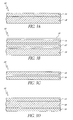
- Figure 3A is a non-limiting embodiment of the improved entry sheet.
- Figure 3B is another non-limiting embodiment of the improved entry sheet.
- Figure 3C is another example of an entry sheet.
- Figure 3D is another non-limiting embodiment of the improved entry sheet.
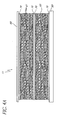
- Figure 4A illustrates an entry sheet provided over a stack of printed circuit boards.
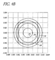
- Figure 4B illustrates graphical representations of True Position Diameter (TPD) and Linear Measurement accuracy measurements provided in a scatter graph.
- FIG. 4C illustrates one method of calculating True Position Radius (TPR).
- Figure 5A is a table showing drill parameters and accuracy measurements of test drill runs comparing the performance of the improved entry sheet with that of other commonly available entry boards.
- Figure 5B is a graph comparatively illustrating the accuracy measurements of Figure 5A .
- Figure 6 is a table illustrating drill parameters and accuracy measurements of test drill runs comparing the performance of the improved entry sheet with other entry boards.
- Figure 7A is a table illustrating drill parameters and accuracy measurements of test drill runs comparing the performance of the entry sheet with an aluminum entry board.
- Figure 7B is a graph comparatively illustrating the accuracy performances of the entry sheet and the aluminum entry board.
- PCB printed circuit board
- electrical interconnect systems electrical interconnect systems
- PCBs comprise systems that generally include a base platform to support the electrical components (for example, a thin board of insulating material) and conductors such as conductive pathways, surfaces, solderable attachments, and the like interconnect the electrical components.
- PCBs can employ a broad range of technologies to support the electrical components (for example, through-hole, surface-mount, mixed-technology, component mounted on one or both sides, etc.) and can comprise a wide range of single or multi-layer constructions (for example, single-sided, double-sided, multilayer, flexible, rigid-flex, stripline, etc).
- the terms broadly describe PCBs at any stage of the manufacturing process, including, for example, multiple PCBs configured into a stack structure to be drilled by drilling machines.
- electronic components broadly defines any device capable of handling electricity and includes systems comprising, for example, digital, analog, analogue-digital, radio frequency, microwave, etc. circuitry and comprises a wide range of electrical systems such as, without limitation, electrical devices, electronic devices, electronic circuits, electrical elements, integrated circuits, hybrid systems, or the like.
- entry sheet is a broad term used in its ordinary sense and includes, without limitation, components provided over the top, at the bottom, and/or within a stack of printed circuit boards during drilling applications, for example, to facilitate drilling holes in the PCBs.
- Entry sheets are provided over one or more PCBs during the drilling process generally, among others, to protect the PCBs, drilling machines and/or their subcomponents from various types of damage arising from the drilling process, to minimize entry burrs, to increase the accuracy with which the holes are drilled in the PCBs, etc.
- Entry sheets are adapted to first accept drill spindles, parts of drilling machines that penetrate PCBs to form holes in the PCBs, before the drill spindles drills the PCBs.
- An entry sheet can comprise one entry sheet layer or a two or more entry sheet layers.
- an entry sheet layer can be provided over another entry sheet layer to form a laminate of the two entry sheet layers using various lamination techniques, such as, for example, adhesives, "cast to foil” process, sputtering, plating, rolling, spraying, etc.
- Entry sheet layer broadly refers to entry sheet subcomponents generally formed from material processed into a thin layer or shape such as a sheet, a film, a foil, or the like.
- Entry sheet layer is broadly defined and comprises a wide variety of entry sheet layer constructions such as, without limitation, substrates, boards, coatings, adhesives, conductive plates, cores, outer shells, lubricants, masks, resist layers, and the like.
- the entry sheet layers can be substantially separate and distinct layers.
- a brad range of materials can be used to manufacture entry sheet layers, including, without limitation, ceramics, fluids (for example, lubricants and solvents), metals, other engineering materials such as additives and fillers, polymers, wood and other natural products, a combination of the above and/or other materials, and the like.
- substrate layer broadly defines an optional entry sheet layer made from relatively rigid materials.
- the substrate layer comprises a broad range of relatively rigid materials, including, by way of non-limiting examples, papers, cotton fabric, asbestos, ceramic material, molybdenum, plastic, glass, glass in various forms such as cloth and continuous filament mat, other organic substances, a combination of the above materials, a combination of one or more of the above materials with other materials, etc.
- Adhesive or “adhesive material” as used herein broadly refer to components and/or materials having uniting or bonding characteristics and also includes adhesive materials, which can be shaped into thin sheets or layers, typically employed for attaching and/or laminating various substructures of multi-layer systems such as circuit boards, PCBs, electrical interconnect systems, entry boards, entry sheets, exit boards, etc.
- Adhesive and “adhesive material” comprise materials used to bond various multi-layer system substructures such as, for example, insulating and/or conducting layers, substrates, boards, surface layers, coatings, masks, or other subcomponents of multi-layer systems.
- Adhesives comprise a broad range of materials, including polymer materials such as, without limitation, epoxies, acrylics, polyimides, modified polyesters, butyral phenolics, other types of resins, or the like.
- adhesives can be used as entry sheet layers in entry sheets and can be configured to reduce entry burrs, protect PCBs, and/or increase drilling accuracy of PCBs.
- adhesives are epoxies.
- drill axis generally refers to an imaginary straight line through the center of a hole to be drilled on PCBs. It is desired for a drill spindle to maintain its position along the drill axis as the drill spindle advances through entry sheets and/or PCBs such that the drill spindle can create holes in accurate locations.
- the terms “drill deflection” or “drill spindle deflect” or “lateral deflection” or “out of position” generally refer to any undesirable deviation, in any direction, of the drill spindle away from a straight course along the drill axis that typically causes the drill spindle, among others, to drill holes in inaccurate positions and/or cause defects in PCBs.
- the terms “drilling” and “drilling applications” are broad terms used in their ordinary sense and include, without limitation, a process of forming holes or channels in a PCB or a stack of PCBs.
- dust as used herein broadly refers to any material, including materials employed to manufacture the entry sheet and/or PCB, that is reduced in size, for example, to dry powdery material. Dust can be sufficiently small in size such that the dust can be readily evacuated from drilling systems using, for example, a drill vacuum.
- epoxy resin broadly refers to thermosetting epoxide polymer materials that are capable of hardening or becoming more solid, for example, when cured.
- Epoxy resin broadly defines multi-component epoxy systems, including two-component epoxy systems, in which a first component comprising epoxy resins is cured into a more solid state by combining the first component with a second component comprising curing agents.
- epoxy resin as used herein also broadly defines single-component systems in which a solution comprising epoxy resin is capable of curing without the need to combine the solution with another solution comprising curing agents.
- epoxy "epoxies,” “epoxy material” broadly refer to polymer material comprising epoxy resin that has partially, substantially, or fully cured.
- curing or “cured” or “cure” broadly defines the process of polymerizing, toughening and/or hardening polymer material by combining polymers such as epoxies with curing agents or by subjecting polymers to other curing processes such as heat, pressure, radiation, or the like.
- “Curing agents” or “curing materials” broadly defines substances or mixtures of substances added to polymer materials to promote or control the curing process. Curing agents may comprise non-curing substances.
- Polymer material can be uncured, partially cured in which the hardening process has begun but is not complete, or fully cured wherein the epoxy resin in the polymer material has substantially or completely hardened.
- Preferably drilling applications utilizing entry sheets as disclosed herein may demonstrate one or more of the following characteristics: improved thru-hole or blind hole (for example, decreased roughness) quality, minimal to no burring, improved drill accuracy, prolonged drill life, decreased drilling temperature, improved ability to increase amount of PCBs drilled at once, and improved ability to drill through PCBs that are typically becoming more difficult to drill through due to increased thicknesses of the PCBs and/or more abrasive circuit board components containing higher T g materials.
- FIG. 1 illustrates one embodiment of a drilling system 1 in which a drilling machine 4 is configured to drill through an entry sheet and at least one electrical interconnect system such as a printed circuit board (PCB) 14.
- the PCB 14 is overlaid with an improved entry sheet 10 configured to reduce or eliminate several problems associated with drilling holes in the PCB 14, such as, for example, scarring, bird nesting, fliers, burring, etc.
- the drilling machine 4 includes a rotating drilling spindle 6 to carry out the drilling and can include a pressure foot 8, for example, to secure the improved entry sheet 10 and/or the PCB 14 in position.
- the drill spindle 6 advances through the polymer sheet 10 and the PCB 14 in succession to thereby create holes in the PCB 14.
- the improved entry sheet 10 is configured to be used in connection with drilling a broad range of drill diameters, including all commonly available drill diameters.
- the improved entry sheet 10 is configured to be used with drill diameters measuring about 6.7 millimeters (mm) or less.
- the improved entry sheet 10 is configured to be used with drill diameters in the range of about 0.10-6.7 mm.
- the improved entry sheet 10 can be used with different drill diameters including drill diameters much less than 0.10 mm and much larger than 6.7 mm.
- Some PCB handlers do not use common entry boards when drilling holes having diameters of 0.25 mm or less because, among others reasons, the common entry boards often break the smaller-sized drill spindles.
- the improved entry sheet 10 is advantageously sufficiently thin such that the improved entry sheet 10 can be used for drill diameters of 0.25 mm or less, thereby enabling the improved entry sheet 10 to provide benefits to the PCBs drilled with those drill diameters, including protecting PCBs from damage, minimizing entry burrs, increasing accuracy of drilled holes, and the like.
- Figure 2 illustrates one example of an entry sheet 10 of Figure 1 configured to be provided over the PCB 14.
- the entry sheet 10 comprises two entry sheet layers, the improved entry sheet component 16 and a substrate layer 18.
- the improved entry sheet component 16 is provided over the substrate layer 18.
- the substrate layer 18 is provided over the PCB 14 and the improved entry sheet component 16 is provided over the substrate layer 18.
- the entry sheet 10 comprising the improved entry sheet component 16 and the substrate layer 18 is provided over the PCB 14 and the drilling spindle 6 drills through the entry sheet 10 and the PCB 14 in succession to create holes in the PCB 14.
- the substrate layer 18 in the preferred embodiment is configured to have a thickness of less than about 6 mils.
- the substrate layer 18 can comprise a thickness in the range of 1-6 mils, including 1-4 mils, 1-3 mils, 1-2 mils, 2-6 mils, 2-5, 2-4 mils, etc.
- the substrate layer 18 has thickness of much less than 1 mil and/or much larger than 6 mils, including 7 mils, 8 mils, 9 mils, etc.
- the entry sheet 10 has a thickness in the range of about 4 mils to 12 mils. In other arrangements, the entry sheet 10 has a thickness in the range of about 4-10 mils, including 4-8 mils, 4-6 mils, 5-12 mils, 5-10 mils, 5-8 mils, 5-7 mils, etc. In still other embodiments, the improved entry sheet 10 has a thickness of more than 12 mils, such as, for example, 13 mils, 14 mils, 15 mils, etc.
- the substrate layer 18 is sufficiently thin so as to not to interfere with the progression of the drill spindle 6 through the improved entry sheet 10 or the PCB 14.
- the substrate layer 18 is advantageously configured to be thin such that as the drill spindle 6 advances through the entry sheet 10, the substrate layer 18 does not form a bird nest at, near or around the tip of the drill spindle 6.
- the substrate layer 18 is configured to be used with drill diameters measuring about 6.7 mm or less.
- the substrate layer 18 is configured to be used with drill diameters in the range of about 0.10-6.7 mm.
- the substrate layer 18 can be used with different drill diameters, including drill diameters much less than 0.10 mm and/or much larger than 6.7 mm.
- the substrate layer 18 can comprise relatively rigid materials such as, for example, metals.
- the substrate layer 18 comprises at least one layer of aluminum.
- the substrate layer 18 further comprises other materials, including, without limitation, papers, cotton fabric, asbestos sheet, ceramic material, molybdenum, other types of plastic, glass in various forms such as cloth and continuous filament mat, etc.
- the substrate layer 18 can also comprise corn paper, soy paper, or other organic substances.
- the substrate layer 18 comprises one or more of the following: high-density fiberboard, medium density fiberboard, metal, metal alloys, paper, melamine, random fiber mats, plastic, chip board, particle board, phenolic, phenolic supported with paper, cloth, or glass fiber, solid phenolic sheets, laminated phenolic sheets. Additionally, by incorporating a stable component such as the substrate layer 18, the entry sheet 10 has increased overall stability and rigidity that results in improved handling characteristics and a reduction in burring and warpage or bending. As one of skill in the art will appreciate, these characteristics will benefit the drilling process.
- the substrate layer 18 comprises flame retardant (FR) pregregs such as, without limitation, FR-2 (cellulose paper impregnated with phenolic resin), FR-3 (cotton paper impregnated with epoxy resin), FR-4 (epoxy-resin impregnated woven glass cloth), FR-5 (woven glass impregnated with epoxy resin), etc. More non-limiting embodiments of the substrate layer 18 that may be used and configured as described herein can be found, for example, on page 8, in the above-specified U.S. Provisional App. No. 60/976,264 .
- the entry sheet 10 comprises the substrate layer 18 configured to minimize entry burrs from occurring during the drilling of the PCB 14.
- the substrate layer 18 is configured to provide structural support to the entry sheet component 16.
- the substrate layer 18 can be configured to protect the top surfaces of the PCB 14 from getting damaged during the drilling process, for example, by the drilling machine 4 or components of the drilling machine 4 such as the drill foot 8.
- the substrate layer 18 comprises relatively rigid materials to sufficiently prevent the drilling machine 4 from impacting one or more layers of the PCB 14.
- the entry sheet component 16 and the substrate layer 18, can be manufactured using various techniques.
- the substrate layer 18 is first provided.
- the entry sheet component 16 is provided over the substrate layer 18 to form the entry sheet 10.
- the entry sheet 10 is provided over PCBs, and the drilling machine 14 drills through the entry sheet 10 and the PCBs 14 in succession to create holes in the PCBs.
- providing the substrate layer 18 comprises selecting suitable material such as aluminum to form the substrate layer 18.
- Providing the entry sheet component 16 comprises selecting suitable entry sheet component material, including polymer material such as epoxy resin as described herein, and processing the suitable entry sheet component material to form the entry sheet component 16. Proceessing the suitable entry sheet component material can comprise partially, substantially, or fully curing one polymer material comprising an epoxy resin. In one embodiment, the polymer material comprising epoxy is cured by curing agents such as amine.
- Providing the entry sheet component 16 also comprises providing an adhesive material, including adhesive material made by curing polymer material such as epoxy resins.
- providing the entry sheet component 16 over the substrate layer 18 comprises forming the entry sheet component 16 onto the substrate layer 18 (for example, coating, depositing, and/or placing the entry sheet component 16 onto the substrate layer 18).
- Providing the entry sheet component 16 over the substrate layer 18 comprises coating, for example, spray-coating (using air or electroless spraying) the entry sheet component 16 onto the substrate layer 18 in a reel-to-reel process.
- the entry sheet component 16 is roller coated onto the substrate layer 18, for example, in a conveyor process.
- the entry sheet component 16 can be provided over the substrate layer 18 and attached to the substrate layer 18 using an adhesive layer (not shown).
- the entry sheet component 16 and the substrate layer 18 are formed using the "cast to foil" process wherein polymer material, including in liquid form, is applied over the substrate layer 18, and the polymer material and the substrate layer 18 are then heated, resulting in a film of the entry sheet component 16 formed on the substrate layer 18.
- suitable substrate materials are deposited onto the entry sheet component 16, for example, by sputtering the suitable substrate materials from a copper cathode.
- the entry sheet component 16 is provided over the substrate layer 18 using a plating process (depositing the substrate layer 18 on the entry sheet component 16).
- suitable substrate material such as aluminum is vaporized in a vacuum chamber and the vapor is deposited on the entry sheet component 16, thereby providing the entry sheet component 16 over the substrate layer 18.
- the entry sheet component 16 can be provided over the substrate layer 18 using other techniques such as curtain coating, crotch coating, slot-die coating, etc.
- forming the entry sheet 10 comprises substantially or fully curing the entry sheet 10, for example, by passing the entry sheet component 16 and the substrate layer 18 through one or more irradiation beams or ovens, for example, as the entry sheet 10 passes through a manufacturing line.
- forming the entry sheet 10 comprises partially curing laminates of the entry sheet component 16 and the substrate layer 18.
- Other non-limiting embodiments of the methods of manufacturing the improved entry sheet component 16 that may be used and configured as described herein can be found, for example, on page 9, in the above-specified U.S. Provisional App. No. 60/976,264 .
- the improved entry sheet 10 comprises an optional top coat 20, the entry sheet component 16, an optional adhesive layer 22, and the substrate layer 18.
- the optional top coat 20 can be configured to reduce, among others, any surface materials that project outwardly from the top surface of the entry sheet component 16 during drilling, including any imperfections in the entry sheet component 16 that, for example, arise from undercuring of the entry sheet component 16 and/or other entry sheet layers of the entry sheet 10.
- the optional top coat 20 can further be configured to enhance the appearance of the improved entry sheet component 16.
- the optional top coat 20 can provide a protective surface over the improved entry sheet 10 so as to minimize the improved entry sheet 10 from sustaining damage during processes related to drilling PCBs such as during transporting the entry sheet component 16.
- the optional adhesive layer 22 can be employed to attach the entry sheet component 16 to the substrate layer 18.
- the optional adhesive layer 22 is configured is different from the entry sheet component 16 that comprises adhesive material in that the optional adhesive layer 22 is configured to laminate or attach entry sheet layers of the entry sheet 10. In some embodiments, the optional adhesive layer 22 is much thinner in thickness than the entry sheet component 16.
- the optional adhesive layer 22 can comprise various adhesive materials, including, without limitation, acrylic materials, polyimides, epoxies, polyesters, phenolic materials, etc. Further non-limiting embodiments of the improved entry sheet component 16 comprising optional layers that may be used and configured as described herein can be found in the above-specified U.S. Provisional App. No. 60/976,264 .
- Figures 1-3B show the entry sheet 10 in particular configurations
- the entry sheet 10 can be provided over PCB 14 in other configurations.
- Figure 3C shows the entry sheet 10 comprising two or more entry sheet layers.
- Figure 3C illustrates the entry sheet 10 comprising one improved entry sheet component 16 provided over another entry sheet component 16
- the entry sheet 10 can comprise the entry sheet component 16 provided over one or more other types of entry sheet layer.
- the entry sheet 10 can comprise two or more entry sheet layers provided over the entry sheet component 16.
- the entry sheet 10 comprises the improved entry sheet component 16 provided over the substrate layer 18, the substrate layer 18 further provided over another entry sheet component 16.
- the entry sheet component 16 can comprise two or more substrate layers 18.
- the improved entry sheet 10 can comprise other optional layers, including, without limitation, coatings, adhesives, lubricants, substrates, solvents, other types of laminates, and/or the like.
- the improved entry sheet 10 comprises at least the improved entry sheet component 16.
- the improved entry sheet component 16 can comprise a wide range of materials, such as, without limitation, ceramics, fluids, metals, polymers, woods, and the like.
- the improved entry sheet component 16 can comprise other materials such as fillers, additives, catalysis, fibers, semiconductors, or the like.
- the improved entry sheet component 16 comprises polymer material, such as, for example, epoxies.
- the improved entry sheet component 16 comprising epoxies, such as adhesive epoxies, provides several advantages, as will be discussed herein.
- the preferred entry sheet component 16 preferably comprises materials that demonstrate one or more of the following characteristics depending on the application: does not interfere with the drill spindle 8; prevents or reduces bird nesting; resists mechanical damage; creates bushings that improve drilling accuracy; resists lateral deflection of the drill spindle 6; is easy to handle; is stable (for example, does not substantially degrade during the life of the product).
- the entry sheet component 16 advantageously comprises material, including polymer material or adhesive material, configured to restrain undesirable deflection of the drill spindle 6 in directions away from the drill axis as the drill spindle 6 advances through the entry sheet 10 and/or the PCB 14, thereby increasing drilling accuracy.
- the drill spindle 6 typically takes a number of revolutions, for example, one, two, three or more revolutions, after entering top surfaces of entry boards and before settling into a desired position, for example, along an axis through the center of the hole to be drilled.
- Bushings cylindrical linings formed from entry sheet material around the drill spindle 6 as the drill spindle 6 advances through the entry sheet component 16 and/or the PCB 14, created during the first few revolutions before the drill spindle 6 is fully positioned at or near the center of the hole to be drilled typically are imperfect and do not effectively restrain the lateral motion of the drill spindle 6 along the drill axis, which can result in a lateral deflection of the drill spindle 6.
- the entry sheet component 16 thus advantageously comprise material, including polymer material such as epoxy, sufficiently strong to hold the drill spindle 6 in position along the drill axis immediately upon or shortly after the drill spindle 6 comes to contact with the entry sheet component 16, creating bushings capable of restraining the drill spindle 6 in position along the desired axis through the center of the hole to be drilled, minimizing or eliminating any lateral deflection and increasing drilling accuracy.
- the improved entry sheet component 16 comprises material, including adhesives or polymer material such as epoxy, sufficiently resistant to mechanical and other types of damage such as scratches, dents, or the like that are caused by, for example, the drill machine 4 and/or the drill foot 8.
- the improved entry sheet component 16 is also configured to resist damage caused by debris, any substance in the drilling system 1 that interferes with the drilling process.
- debris or “waste substances” broadly define substances present in the drilling system 1 that interfere with the drilling process and include, for example, dust particles, entry sheet and/or PCB materials that are removed as holes are created therein, or the like.
- Debris can cause mechanical damages on top surfaces or other portions of common entry boards that can deflect the drill spindle 6 out of position, causing the drill spindle 6 to drill holes in an inaccurate position or to otherwise damage existing holes or other parts of the PCB 14.
- debris cause substantial hole defects which can lead to fliers, a common problem in which defects even in just a few holes (for example, a few out of 50,000 holes) can render the entire PCB inoperable.
- the improved entry sheet component 16 is advantageously configured to resist various types of damage, including mechanical damage, thereby minimizing undesired deflection of the drill spindle 6 arising from such damage.
- the improved entry sheet component 16 is advantageously configured to readily reduce to dust during the drilling process.
- the entry sheet component 16 comprises material, including adhesives and/or polymer material such as epoxies, which readily reduces to dust during the drilling process to thereby eliminate or minimize a common problem known as bird nesting. Bird nesting occurs when entry sheet materials fail to sufficiently degrade to dust as the drill spindle 6 advances through the entry boards, and waste substance accumulates around the tip of the drill spindle 6, interfering with progression of the drill spindle 6 through entry boards or the various layers of the PCB 14.
- heat generated by the drilling process affects the chemical property of some commonly available entry boards (for example, melting portions of the entry boards) such that the entry boards fail to effectively reduce to dust.
- some entry sheets fail to degrade to dust unless the drill spindle 6 reaches undesirably high temperatures that may otherwise damage components of the circuit boards.
- the size of waste substance that accumulates at the tip of the drill spindle 6 continues to increase in size as the drill spindle 6 further advances through the entry boards or layers of the PCB 14, thereby exacerbating the degree with which the bird nest (waste substance accumulating on or around the drill spindle 6) interferes with the drilling operation and/or accuracy.
- the resistance created by the accumulating waste substance causes the drill spindle 6 to break, introducing undesirable debris to the system, necessitating more frequent and expensive drill spindle replacements, and also potentially substantially damaging the PCBs.
- the waste substance additionally can cause the drill spindle 6 to deflect out of its position, decreasing the accuracy with which the holes are created in the PCB 14 and/or damaging the PCB 14.
- the improved entry sheet component 16 preferably comprises material, including adhesive material, that readily reduces to dust during the drilling process so as to minimize or avoid the problems associated with bird nesting, including, without limitation, drill deflection, drill spindle damage, etc.
- the entry sheet component 16 comprises material, including polymer material, configured to reduce to dust as the drill spindle 16 advances through the entry sheet component 16.
- the entry sheet component 16 reduces to dust upon contact with the drill spindle 6.
- the entry sheet component 16 that is reduced to dust can effectively be evacuated, for example, by a vacuuming mechanism associated with the drilling machine 4.
- the entry sheet component 16 preferably comprises material, including polymer material, having thermal characteristics such that the entry sheet component 16 can withstand heat generated by the drilling process.
- the entry sheet component 16 readily degrades to dust even under the heat of the drill without melting, oozing, or running, thereby minimizing or eliminating waste substance from forming around the drill spindle 6.
- the entry sheet component 16 comprises polymer material, including epoxies, which reduces to dust under common drilling temperatures.
- the entry sheet component 16 comprises adhesives or polymer material, including, without limitation, epoxies.
- the entry sheet component 16 comprises adhesive material, including adhesives typically configured for different purposes than to facilitate drilling PCBs (attaching various layers of PCBs, entry sheets, backup boards, or the like).
- Adhesives are typically selected for bonding various internal and external layers of PCBs based on adhesive characteristics such as bond strength, dimensional stability, heat resistance, electrical properties, etc.
- the entry sheet component 16 comprises adhesive material configured to facilitate the drilling process, for example, by minimizing entry burrs, increasing accuracy, protecting the PCB 14 from damage, etc.
- the entry sheet 10, and the entry sheet component 16 can comprise adhesive material for purposes other than to bond layers of the entry sheet 10 together.
- the improved entry sheet component 16 comprises adhesives provided as coatings over substrates made from rigid material, such as the substrate layer 18 of Figure 3A . Adhesives such as acrylics, polyimides, epoxies, modified polyesters, butyral phenolics, or the like are suitable for use as the entry sheet component 16.
- the entry sheet component 16 comprises commercially available products (for example, Daubert's Doubond 17092, 18973, 19102, 19109, 19112, 19116).
- the entry sheet component 16 can also comprise resins selected from thermosetting or thermoplastic families of resins, for example, fabricated in sheet form.
- the entry sheet component 16 can comprise thermoplastic materials such as polyester, polyimide, polyetherimid, polycarbonate, cellulose triacetate, a combination of two or more of the above materials, or a combination of one or more of the above materials with other materials.
- the entry sheet component 16 comprises thermoplastic polymer resins of the polyester family, including, without limitation, polyethylene terephthalate, which is sometimes referred to as Mylar, including SDI's smooth Mylar.
- the entry sheet component 16 comprises one or more thermosetting materials such as cured epoxy resins, phenolic resins, amine resins, polyvinylacetals, or the like, for example, formed into a thin layer.
- the entry sheet component 16 comprises epoxies.
- the epoxies can be of the type bisphenol a/epichlorohydrin.
- preferred epoxies include, but are not limited to, two-part room temperature cured epoxies, polyimide cured epoxies, two-part bisphenol a epoxies, and diglycidyl ether of bisphenol a epoxies.
- epoxies can comprise an epoxy resin base and curing agents such as amines, polyamines, amides, polyamides, cycrloaliphatic agents, other appropriate agents, etc.
- the entry sheet component 16 comprises other curing and non-curing materials.
- the entry sheet component 16 comprises ether, including, for example, glyeidyl ether, alkyl glycidyl ether (for example, CAS# 68609-97-2), and the like.
- the entry sheet component 16 can also comprise other materials including, without limitation, carbonates such as calcium carbonate (for example, CAS# 1317-65-3), proprietary epoxies, titanium dioxide (for example, CAS# 13463-67-7), coloring agents such as yellow pigment (CAS# 51274-00-1), etc.
- the entry sheet component 16 comprises triethylenetetramine (for example, CAS# 112-24-3).
- the entry sheet component 16 can comprise phenols such as nonyl phenols (for example, CAS# 84852-15-3).
- phenols such as nonyl phenols (for example, CAS# 84852-15-3).
- Other non-limiting embodiments of the improved entry sheet component 16 that may be used and configured as described herein can be found, for example, on page 8, in the above-specified U.S. Provisional App. No. 60/976,264 .
- the entry sheet 10, including the entry sheet component 16, in some particular embodiments is formed by combining epoxy resins, curing agents consisting essentially of polyamidoamine, and a third group of materials consisting essentially of calcium carbonate, triethylene tetramine, polyethylenepolyamine, titanuium dioxide, glycidyl ether, and nonyl phenol.
- the epoxy resin can be of the type bisphenol a/epichlorohydrin.
- the improved entry sheet component 16 comprises a two-component polymer material wherein a first solution is combined with a second solution to form the entry sheet component 16.
- the first solution can comprise epoxy resins, including adhesive epoxy resins, combined with a second solution such that the second solution cures the epoxy resins present in the first solution, thereby forming the entry sheet component 16.
- the two-component polymer material comprises the first solution and the second solutions in equal volumes.
- the first solution and the second solution having different volumes are combined to form the entry sheet component 16.
- the second solution comprises curing agents configured to cure the epoxy resins present in the first solution.
- the second solution comprises curing agents consisting essentially of aliphatic amines and polyamidoamines.
- the first solution comprises epoxy resin (for example, CAS# 25068-38-6).
- combining the first solution with the second solution partially cures the epoxy resin present in the first solution.
- combing the first solution with the second solution fully cures the epoxy resin present in the first solution.
- the epoxy resin can comprises the bulk of the material of the first solution of the entry sheet component 16.
- the first solution comprises bisphenol a/epichlorohydrin epoxy resin, including at about 55-95% by weight, including about 85-95% by weight, about 80-90% by weight, about 55-85% by weight, about 55-75% by weight, about 55-65% by weight, about 65-85% by weight, about 65-95% by weight, about 65-75% by weight, about 75-90% by weight, etc.
- the first solution comprises bisphenol a/epichlorohydrin epoxy resin at about 55-90% by weight, including about 60-70% by weight.
- the first solution comprises another epoxy resin, including, for example, proprietary epoxy resins.
- the first solution comprises the bisphenol a/epichlorohydrin epoxy resin at about 80-95% by weight, including about 80-90% by weight and/or about 85-95% by weight, and comprises the other epoxy resin at about 5-15% by weight.
- the first solution comprises one or more ethers, including glycidyl ethers at about 1-20%, including about 1-10% and about 1-5% by weight.
- Suitable glycidyl ethers include alkyl glycidyl ethers (for example, CAS# 68609-97-2 or C12-C14 alkyls).
- Additives may also be included in the first solution of the entry sheet component 16.
- the first solution comprises additives such as colorants and some salts at a relatively low portion by weight, for example, on the order of about 1-2% or about 1-5%.
- the amount of salt, such as calcium carbonate, present in the first solution is as much as about 25-45% by weight, including about 25-40% by weight, about 25-35% by weight, about 30-40% by weight, etc.
- the first solution comprises titanium dioxide less than 2% by weight and/or yellow pigment less than 2% by weight.
- Other non-limiting embodiments of the improved entry sheet component 16 that may be used and configured as described herein can be found, for example, on page 8, in the above-specified U.S. Provisional App. No. 60/976,264 .
- the entry sheet component 16 is formed by combining the first solution comprising epoxy resins with the second solution, for example, to cure the epoxy resins present in first solution, thereby forming the entry sheet component 16.
- the first solution is combined with the second solution, the second solution comprising curing agents to sufficiently cure the resin, including epoxy resin, present in the first solution.
- the entry sheet component 16 can be formed from the second solution, the second solution comprising curing agents such as amines, polyamines, amides, polyamides, cycrloaliphatic agents, other appropriate polymerizing agents, or the like.
- the second solution comprises materials such as, without limitation, polethylenepolyamine, polyamidoamine, triethylenetetramine, or the like.
- the second solution comprises curing material wherein amine forms the bulk of the material.
- the second solution comprises amine, such as, for example, polyamidoamine, at about 50-88% by weight, including about 50-70% by weight, about 50-75% by weight, about 84-88% by weight, about 55-75% by weight, about 55-65% by weight, about 55-60% by weight, about 65-85% by weight, about 75-85% by weight, etc.
- the second solution comprises amine greater than 80% by weight.
- the second solution can comprise about 50-70% by weight polyamidoamine, including about 50-60% by weight and about 60-70% by weight.
- the second solution comprises less than about 10% by weight of polyethylenepolyamine.
- the second solution can comprise amine typically provided in adhesive materials at about 84-88% by weight.
- the second solution comprises one or more carbonates, including calcium carbonates, at about 25-45%, including about 25-35% and about 35-45% by weight.
- Other materials can be included in the second solution such as, without limitation, nonyl phenol and/or triethylenetetramine.
- the second solution comprises nonyl phenol and/or triethylenetetramine of low concentrations, for example, on the order of about 1-16% by weight. In yet other embodiments, the second solution comprises less than 10% by weight of triethylenetetramine and about 12-16% by weight of nonyl phenol.
- the improved entry sheet component 16 and other commonly used and comparable entry sheets were provided over different configurations of PCBs in varying test environments and the entry sheets and the PCBs were drilled in succession in realistic settings so as to determine the performance of the various entry sheets.
- the test drill parameters and performance measurements are described in Examples 1-7 below.
- the improved entry sheet 10 comprising the entry sheet component 16 and the substrate layer 18 as described in this application was used.
- the entry sheet component 16 comprised epoxy adhesive formed from polymer material comprising bisphenol a/epichlorohydrin epoxy resin.
- the substrate layer 18 comprised aluminum.
- the improved entry sheet component 10 comprising the entry sheet component 16 formed from Mylar material was used.
- C pK Process Capability Index
- TPD True Position Diameter
- TPR True Position Radius
- C pK a six-sigma compatible statistical tool, measures process capability, the ability of a process to produce outputs within specification limits or tolerance levels.
- C pK predicts performances of systems or processes based upon collected test data and indicates process capability taking into account the effect of non-centered data distribution.
- Process capability is a validation technique often employed to qualify a particular PCB drilling process or PCB drill machine system.
- C pK measures how close a drilling machine is running to its specification levels relative to the variability of the process and, therefore, the larger the C pK , the less likely the drilling machine drills outside of the tolerance level.
- C pK of 1.33 or higher is preferred in manufacturing processes, including drilling printed circuit boards.
- One of the objects of Examples 1-7 is to show that drilling printed circuit boards using the improved entry sheet component 16 improves the drilling process by enabling drilling machines to operate closer to their operational capabilities than other entry sheets.
- careful consideration was exercised to maintain a consistent drilling environment so as to ensure that the contribution to process capability made by the tested entry sheets was satisfactorily attributable to the entry sheets and not to other factors such as drilling machine control, configuration of cutting tool, gripping arrangement, precision of drilling spindle, etc.
- a C pK analysis of acceptance trials often entails scatter plots indicating the degree of scatter around a nominal target point, the nominal target point being the position of the ideal accurate hole.
- the improved entry sheet 10 is configured to provide C pK values in the range of about 0.91-2.93, including 1.0-2.8, 1.0-2.7, 1.8-2.6, 1.5-2.5, 1.7-2.3, etc.
- TPD describes the actual diameter of the area that is occupied by the data.
- Figure 4B shows the circles 79 illustrating TPD values of various diameters on a scatter graph.
- TPR is related to TPD and describes the actual radius of the area that is occupied by the data and is 1 ⁇ 2 TPD.
- TPR is calculated, as shown in Figure 4C , by determining the distance between a center 83 of a drilled hole 82 and a center 84 of a nominal hole 81, the nominal hole 81 being the position of the ideal accurate hole.
- TPR is provided in inches.
- a lower TPR is desired in drill systems because the lower the TPR for a drilled hole, the closer the center 83 of the drilled hole 82 is to the center 84 of the nominal hole 81, indicating a more accurate positioning of the drilled hole 82.
- the improved entry sheet 10 is configured to provide TPR values, in inches, the range of about 0.00106 to 0.00690, including 0.00110-.00680, 0.00120-.00600, 0.00125-.00500, etc.
- Linear measurements describe the amount of error in the X & Y axis, the graphical representation of which is illustrated as a rectangle 78 in Figure 4B .
- a smaller linear measurement indicates a more accurately positioned drilled hole.
- Analyzing accuracy measurements in a linear fashion is more limited than other radial measurements because the drill data of holes results in a circular pattern. Nevertheless, linear measurement data for Example 4 is provided. Further non-limiting discussions of accuracy measurements related to the improved entry sheet component 16 that may be used and configured as described herein can be found, for example, on page 5-6 and in Appendix A and B, in the above-specified U.S. Provisional App. No. 60/976,264 .
- Figure 4A shows a panel 11 on which drilling was carried out in Example 1 to determine the influence of the improved entry sheet component 16 on drill accuracy and to compare the performance of the improved entry sheet component 16 with other entry sheets.
- the panel 11 comprises an entry sheet 68, and a stack of PCBs having first and second dielectric layers 60, 61, each dielectric layer 60, 61 being a double-sided laminate having conductive layers 70 on each surface, the conductive layers 70 having 1 ounce copper material, and a backup board 80.
- Four different entry sheets were provided as the entry sheet 68 to drill the panel 11, as described further herein.
- the first and second dielectric layers 60, 61, the conductive layers 70, the backup board 80 were selected so as to provide a realistic representation of drilling in production. Accordingly, overlaying the entry sheet 68 over the stack of PCBs and drilling the entry sheet 68 and the stack of PCBs in succession provided information on how each of the entry sheets 69 perform when used in real-life applications.
- Each of the first and second dielectric layers 60, 61 comprised 0.059 inch thick, double-sided ISOLA FR-4 laminate.
- a 0.093 inch LCOA Tek board was used as the backup board 80.
- the panel 11 was drilled using four different types of entry sheets as the entry sheet 68: (1) 0.012 inch LCOA EO+, an entry sheet manufactured and sold by Laminated Company of America (LCOA) having aluminum laminated to both sides of a cellulose core; (2) 0.007 inch solid aluminum entry board (3303 Alloy - H19 hardness); (3) 0.014 inch lubricated entry (LE) sheet, an entry sheet manufactured and sold by Mitsubishi Gas Chemical Company, Inc. having a lubricating layer and an aluminum sheet; and (4) 0.009 inch entry sheet component 16 comprising the entry sheet component 16 and the substrate layer 18.
- the improved entry sheet component 16 in Example 1 comprised a 0.006 inch entry sheet component 16 provided over a 0.003 inch substrate layer 18.
- Each one of the four entry sheets was drilled using the same Excellon Concept I single-spindle machine so as to minimize variation.
- the drill parameters of the Excellon Concept I drill machine as used in Example 1 were as follows: 0.0135 inch drill diameter; 0.220 inch drill flute length; 110,000 rpm drill speed; 88 ipm feed; 800 ipm retract; and 2020 max hits.
- Example 1 The performances of each of the four entry sheets in Example 1 were measured in consistent test environments to minimize undesired accuracy measurement variances arising from differences in test parameters such as lighting methods, camera resolution, quality of the optics, magnification, algorithms used to identify the actual edge of drilled holes, etc.
- Accuracy measurements for each of the four entry sheets were obtained on an Excellon Concept I with an ITRAN Vision System. Two 0.0453" diameter holes were used to align the vision system to the drilled pattern formed on the panels 11.
- Four of the panels 11 each including one of the four entry sheets were sent through a high-pressure air spray to remove any debris remaining in the holes so as to increase the reliability of the results obtained from a vision system.
- the panels 11 were allowed to stabilize with the Vision System for 48-hours prior to analyzing the drill data.
- Example 1 the actual location of the drilled hole position was determined from measuring the location of the drilled hole at the top of the panel 11.
- the Excellon Concept I projected light atop the panel 11 and, using an algorithm, identified 96 points around the circumference of the hole to determine the best fit for a circle.
- Figure 5A illustrates the panel 11 configuration, drill machine parameters, and accuracy measurements for the drill tests in Example 1.
- Figure 5A illustrates C pK and TPR (in inches) values for a +/-0.0015 inch tolerance level, which is equivalent to about a 0.00212 inch TPR.
- the position of the holes formed on the panel 11 drilled with the improved entry sheet component 16 were the most accurate at 2.93 C pK in comparison with C pK values of 1.59, 2.3, and 2.8 for the LOCA EO+, aluminum, and LE sheet entry sheets.
- Example 2 the improved entry sheet component 16 and an LE sheet entry sheet were provided over a PCB panel, and the entry sheets and the PCB panels were drilled in succession.
- the rows associated with Example 2 in Figure 6 show the configuration of the PCBs, drill parameters of the drill machine, and the accuracy measurements resulting from the test drill run of Example 2. Drilling in Example 2 was conducted to compare the performance, including accuracy measurements, of the 0.009 inch thick entry sheet component 16 with a 0.014 inch thick LE sheet entry sheet.
- the improved entry sheet component 16 in Example 2 comprised a 0.006 inch entry sheet component 16 provided over a 0.003 inch substrate layer 18, the substrate layer 18 comprising aluminum.
- the entry sheets were provided over a 0.1100 inch thick stack of 1-high 26-layer PCB having FR-406 dielectric layers and 1 ⁇ 2 ounce outer copper conductive layer and 2 ounce internal copper layers.
- Each of the improved entry sheet component 16 and the LE sheet entry sheet were provided over PCB stacks supported by exit boards.
- the improved entry sheet component 16 was tested in combination with a SlickBack backup board (.095 inch thick) and the LE sheet entry sheet was tested in combination with a 0.096 inch thick STARboard back up board.
- An Excellon Century 2001 drilling machine was used to drill the PCB stacks in Example 2, the drilling machine having the following parameters: 0.0098 inch drill diameter; 0.185 inch drill flute length; 125,000 rpm drill speed; 114 ipm feed; 600 ipm retract; and 2200 max hits. Accuracy measurements in Example 2 were taken from the bottom of the PCB stack for linear tolerances of +/-0.002 inches.
- the LE sheet entry sheet resulted in a C pK of 0.56 and a TPR of 0.00355 whereas the improved entry sheet component 16 attained increased accuracy at a C pK of 0.91 and TPR of 0.00276.
- Example 2 the improved entry sheet component 16 in Example 3 comprised a 0.006 inch entry sheet component 16 provided over a 0.003 inch substrate layer 18, the substrate layer 18 comprising aluminum.
- the entry sheets were provided over a 0.098 inch thick, 1-high, 18-layer PCB having FR-406 dielectric layers, 1 ⁇ 2 ounce outer and 1 ounce internal copper conductive layers.
- Each of the improved entry sheet component 16 and the LE sheet entry sheet were provided over PCB stacks supported by exit boards, the improved entry sheet component 16 being tested in combination with a SlickBack backup board (.096 inch thick) and the LE sheet entry sheet being tested in combination with a STARboard backup board (.095 inch thick).
- An Excellon Century 2001 drilling machine was used to drill the PCB having the following drilling parameters: 0.0079 inch drill diameter; 0.118 inch drill flute; 125,000 rpm drill speed; 55 ipm feed; 700 ipm retract; and 500 max hits.
- the rows associated with Example 3 in Figure 6 the LE sheet entry sheet resulted in a C pK of 0.53 and a TPR of 0.00310.
- the improved entry sheet component 16 attained better accuracy measurements of a 0.92 C pK and a TPR of 0.00226.
- Example 3 illustrates C pK and TPR values for +/-0.002 inch tolerance levels.
- Improved entry sheet component CPK Standard Deviation Position Linear: 0.90 X: 0.000685 Radius: .00226 Radial: 0.92 Y: 0.000741 Diameter: 0.00452 Radial: 0.000442 Diameter Tolerance: 0.005445 LE Sheet CPK Standard Deviation True Position Linear: 0.74 X: 0.00085 Radius: 0.0031 Radial: 0.53 Y: 0.000901 Diameter: 0.0062 Radial: 0.000572 Diameter Tolerance: 0.007319
- Example 4 illustrates the performances of the improved entry sheet component 16 in comparison with a 0.007 inch thick aluminum entry board.
- the improved entry sheet component 16 in Example 4 comprised a 0.006 inch entry sheet component 16 provided over a 0.003 inch substrate layer 18, the substrate layer 18 comprising aluminum.
- the entry sheets were provided over a 0.098 inch thick stack of a 1-high 18-layer PCB having FR-406 dielectric layers, 1 ⁇ 2 ounce outer and 1 ounce internal copper conductive layers.
- Each of the improved entry sheet component 16 and the LE sheet entry sheet were provided over PCB stacks supported by exit boards.
- the improved entry sheet component 16 was tested in combination with a SlickBack backup board (096 inch thick) and the LCOA EO+ board was tested in combination with a 0.095 inch STARboard back up board.
- An Excellon Century 2001 drilling machine was used to drill the PCB having the following drilling parameters: 0.0079 inch drill diameter; 0.118 inch drill flute; 125,000 rpm drill speed; 55 ipm feed; 700 ipm retract; and 1500 max hits.
- the improved entry sheet component 16 attained increased accuracy at a C pK of 1.76 and a TPR of 0.00160 in comparison with the LE sheet entry sheet (C pK of 1.36 and TPR of 0.00291).
- Example 5 the improved entry sheet component 16 and a 0.007 inch aluminum entry board were provided over a 0.062 inch thick stack of a 1-high, 2-layer PCB having FR-408 dielectric layers and 1 ounce outer copper layers.
- Each of the PCBs in Example 5 were supported by Spectrum Gold exit boards.
- a Hitcahi Union Tool drilling machine was used to drill each of the PCBs in Example 5, the drilling machine having the following drilling parameters: 0.0079 inch drill diameter; 0.118 inch drill flute; 120,000 rpm drill speed; 79 ipm feed; 500 ipm retract; and 2000 max hits.
- the improved entry sheet component 16 resulted in a C pK of 1.66 and a TPR of 0.00150.
- the aluminum entry board obtained less accurate measurements of a C pK of 1.11 and a TPR of 0.00244.
- Example 6 the improved entry sheet component 16 and a 0.007 inch aluminum entry board were provided over a 0.093 inch thick stack of 1-high, 2-layer PCBs having FR-4 dielectric layers and I ounce outer copper layers. Each of the PCBs in Example 6 were supported by SlickBack exit boards (.096 inch thick). A Hitcahi drilling machine was used to drill each of the PCBs in Example 6, the drilling machine having the following drilling parameters: 0.0098 inch drill diameter; 0.187 inch drill flute; 125,000 rpm drill speed; 87 ipm feed; 700 ipm retract; and 2020 max hits.
- Each of the improved entry sheet component 16 the aluminum entry board were overlaid on the PCBs and the entry sheets and the PCBs were drilled in succession.
- Six entry sheets 10 and 6 aluminum entry boards were each provided over different PCBs, and the entry sheets and PCBs were drilled in succession to assess the performance of the entry sheets given a +/-0.002 inch upper specification TPR tolerance level.
- the C pK values for each of the 6 drill runs in Example 6 were higher for the improved entry sheet component 16 (C pK of 2.61, 1.47, 1.94, 1.56, 1.83, and 1.03 for drill runs a, b, c, d, e, and f) when compared with the aluminum entry board (C pK of 1.00, 0.75, 1.18, 0.67, 0.67, and 0.52 for drill runs a, b, c, d, e, and f).
- the improved entry sheet component 16 performed well under the +/-0.002 inch upper specification tolerance level for each of the drill runs with TPR values, in inches, of 0.00128, 0.00167, 0.00145, 0.00156, 0.00142, and 0.00182 for drill runs a, b, c, d, e, and f.
- Example 7 the improved entry sheet component 16 of Figure 3B comprising the entry sheet component 16 was provided over a panel having two layers of 0.059 inch thick double-sided boards, the boards having FR-4 laminates and 0.51 ounce outer copper layers.
- the improved entry sheet component 16 comprised the 4 mil thick entry sheet component 16 having thermoplastic polymer resins of the polyester family such as polyethylene terephthalate, and more particularly, material comprising Mylar.
- the panel was drilled using a 60300135 drill Tulon having the following parameters: 0.0135 inch drill diameter; 0.118 inch drill flute; 110,000 rpm drill speed; 88 ipm feed; 800 ipm retract; and 2000 max hits.
- the improved entry sheet component 16 comprising the entry sheet component 16 resulted in a C pK of 3.54 and a TPR of 0.00063.
- the improved entry sheet 10 as described in various embodiments herein provides significant improvements, including, without limitation, in location accuracy and damage resistance compared to other commonly available entry boards. After evaluating all of the available data from the above testing, it is further possible also to conclude that the improved entry sheet component 16 provides benefits that can contribute to, among others, reducing the height of entry burrs.
- the coated entry material can enhance the process window and allow better overall results that may contribute to reduced scrap levels and reduced costs for PCB fabrication.
Landscapes
- Engineering & Computer Science (AREA)
- Manufacturing & Machinery (AREA)
- Microelectronics & Electronic Packaging (AREA)
- Mechanical Engineering (AREA)
- Perforating, Stamping-Out Or Severing By Means Other Than Cutting (AREA)
- Drilling And Boring (AREA)
- Chemical & Material Sciences (AREA)
- Organic Chemistry (AREA)
Claims (13)
- Eingangsfolie (10) zum Bohren von Leiterplatten (14) mit einem Bohrwerkzeug, wobei das Bohrwerkzeug von oben in die Eingangsfolie (10) in einem bestimmten Bohrbereich eindringt, wobei die Eingangsfolie (10) umfasst:Eine ebene, geschichtete Substratschicht (18) mit einer Stärke von ungefähr 0,1524 mm oder weniger und daran angepasst, über zumindest eine zu bohrende bestückte Leiterplatte angeordnet zu werden, worin die Substratschicht (18) eine untere Oberfläche und eine obere Oberfläche aufweist, worin die untere Oberfläche an die obere Oberfläche der mindestens einen zu bohrenden bestückten Leiterplatte angrenzt, undein Eingangsfolienbestandteil (16), bereitgestellt über der oberen Oberfläche der Substratschicht, worin der Eingangsfolienbestandteil (16) eine Stärke von ungefähr 0,1524 mm oder weniger aufweist;worin die Substartschicht (18) wenigstens eine Schicht aus Aluminium umfasst,worin der Eingangsfolienbestandteil (16) in einer Einzelschicht eine Beschichtung umfasst, die auf die obere Oberfläche der Substartschicht (18) aufgebracht ist, so dass das Bohrwerkzeug während des Bohrens der Leiterplatte (14) zuerst durch die Beschichtung dringt, worin der Eingangsfolienbestandteil (16) eine vollständig ausgehärtete, vollständig duroplastische Epoxidharz-Klebezusammensetzung umfasst, worin die Zusammensetzung umfasst:Bisphenol A / Epichlorhydrin-basiertes Epoxid, undein Aushärtemittel, dadurch gekennzeichnet, dassdie vollständig ausgehärtete, vollständig duroplastische Epoxidharz-Klebezusammensetzung weiterhin ein Salz umfasst, das zwischen ungefähr 25 und ungefähr 45 Gewichts-% des Eingangsfolienbestandteils (16) ausmacht, basierend auf dem Gesamtgewicht des Eingangsfolienbestandteils (16).
- Eingangsfolie (10) nach Anspruch 1,
worin die Eingangsfolie (10) eine Stärke in dem Bereich von ungefähr 0,1016 bis 3,048 mm aufweist, oder
worin die Substartschicht (18) eine Stärke in dem Bereich von ungefähr 0,0254 bis 0,1524 mm aufweist, oder
worin der Eingangsfolienbestandteil (16) eine Stärke in dem Bereich von ungefähr 0,0762 bis 0,1524 mm aufweist, oder
worin die Eingangsfolie (10) angepasst ist, mit Bohrdurchmessern in dem Bereich von ungefähr 0,1 bis 6,7 mm verwendet zu werden. - Eingangsfolie (10) nach Anspruch 1, worin die Substratschicht (18) weiterhin umfasst:Eine hochdichte Faserplatte, eine Faserplatte mittlerer Dichte, Metall, Metalllegierungen, Papier, Melamin, beliebige Fasermatten, Kunststoff, eine Pressspanplatte, Phenolharz, mit Papier gestütztes Phenolharz, Stoff oder Glasfaser, feste Phenolharzlagen oder laminierte Phenolharzlagen.
- Eingangsfolie (10) nach Anspruch 1, worin der Eingangsfolienbestandteil (16) angepasst ist, mit Bohrdurchmessern in dem Bereich von ungefähr 6,7 mm oder weniger verwendet zu werden.
- Eingangsfolie (10) nach Anspruch 4,
worin der Eingangsfolienbestandteil (16) angepasst ist, einem seitlichen Ausschlag der zum Bohren der Löcher in die Leiterplatten (14) verwendeten Bohrspindeln stand zu halten, oder
worin die Eingangsfolie (10) angepasst ist, zu Staub zu zerfallen, oder
worin der Eingangsfolienbestandteil (16) angepasst ist, mechanischen Beschädigungen zu widerstehen. - Eingangsfolie (10) nach Anspruch 5, worin die Substratschicht (18) weiterhin umfasst:Eine hochdichte Faserplatte, eine Faserplatte mittlerer Dichte, Metall, Metalllegierungen, Papier, Melamin, beliebige Fasermatten, Kunststoff, eine Pressspanplatte, Phenolharz, mit Papier gestütztes Phenolharz, Stoff oder Glasfaser, feste Phenolharzlagen oder laminierte Phenolharzlagen.
- Verfahren zum Bohren einer Leiterplatte (14), wobei das Verfahren umfasst:Bereitstellen einer Eingangsfolie (10) nach Anspruch 1, undBohren des Eingangsfolienbestandteils (16), der Substratschicht (18) und der Leiterplatte (14) in dieser Reihenfolge, um ein Loch in der Leiterplatte (14) zu erzeugen.
- Verfahren nach Anspruch 7,
weiter umfassend Bereitstellen der Substratschicht (18) in einer Stärke im Bereich von ungefähr 0,0254 bis 0,1524 mm, oder
weiter umfassend Bereitstellen der Eingangsfolienbestandteil (16) in einer Stärke in dem Bereich von ungefähr 0,0762 bis 0,1524 mm, oder
weiter umfassend Bereitstellen der Eingangsfolie (10), die angepasst ist, mit Bohrdurchmessern in dem Bereich von ungefähr 0,1 bis 6,7 mm verwendet zu werden. - Verfahren nach Anspruch 8, wobei das Klebeepoxid Kalziumkarbonat, Triethylentetraamin, Polyethylenpolyamin, Titandioxid, Glycidylether oder Nonylphenol umfasst.
- Verfahren zur Herstellung der Eingangsfolie (10) nach Anspruch 1, wobei das verfahren umfasst:Bereitstellen einer Substratschicht (18) umfassend mindestens eine Schicht Aluminium,Bilden eines Eingangsfolienbestandteils (16) durch Zusammenführen von Polymermaterial umfassend ungefähr 55-95 Gewichts-% Bisphenol A / Epichlorhydrin-basiertes Epoxid mit einem Aushärtemittel und einem Salz, undBereitstellen des Eingangsfolienbestandteils (16) über der Substratschicht (18).
- Verfahren nach Anspruch 10, wobei das Bereitstellen des Eingangsfolienbestandteils (16) über dem Substrat ein Beschichten durch Sprühen, Beschichten durch Aufrollen, ein Gießbeschichten, Schrittbeschichten oder Schlitzdüsenbeschichten des Eingangsfolienbestandteils (16) über die Substratschicht (18) umfasst.
- Verfahren nach Anspruch 10,
wobei das Aushärtemittel Polyamidoamin umfasst, vorzugsweise worin das Aushärtemittel Polyamidoamin in ungefähr 50-88 Gewichts-% umfasst, oder
wobei das Aushärtemittel Kalziumkarbonat, Triethylentetraamin, Polyethylenpolyamin, Titandioxid, Glycidylether oder Nonylphenol umfasst. - Verfahren nach Anspruch 10, wobei die Substratschicht (18) weiterhin umfasst: Eine hochdichte Faserplatte, eine Faserplatte mittlerer Dichte, Metall, Metalllegierungen, Papier, Melamin, beliebige Fasermatten, Kunststoff, eine Pressspanplatte, Phenolharz, mit Papier gestütztes Phenolharz, Stoff oder Glasfaser, feste Phenolharzlagen oder laminierte Phenolharzlagen.
Applications Claiming Priority (2)
| Application Number | Priority Date | Filing Date | Title |
|---|---|---|---|
| US97626407P | 2007-09-28 | 2007-09-28 | |
| PCT/US2008/078012 WO2009045932A1 (en) | 2007-09-28 | 2008-09-26 | Improved systems and methods for drilling holes in printed circuit boards |
Publications (2)
| Publication Number | Publication Date |
|---|---|
| EP2191701A1 EP2191701A1 (de) | 2010-06-02 |
| EP2191701B1 true EP2191701B1 (de) | 2013-03-20 |
Family
ID=40293639
Family Applications (1)
| Application Number | Title | Priority Date | Filing Date |
|---|---|---|---|
| EP20080836066 Not-in-force EP2191701B1 (de) | 2007-09-28 | 2008-09-26 | Eingangsfolie, herstellungsverfahren dafür und verfahren zur bohrung von löchern in bestückten leiterplatten |
Country Status (5)
| Country | Link |
|---|---|
| US (3) | US8323798B2 (de) |
| EP (1) | EP2191701B1 (de) |
| JP (1) | JP2010540260A (de) |
| CN (1) | CN101878678A (de) |
| WO (1) | WO2009045932A1 (de) |
Families Citing this family (40)
| Publication number | Priority date | Publication date | Assignee | Title |
|---|---|---|---|---|
| US8323798B2 (en) | 2007-09-28 | 2012-12-04 | Tri-Star Laminates, Inc. | Systems and methods for drilling holes in printed circuit boards |
| JP2010264576A (ja) * | 2009-05-18 | 2010-11-25 | Fujikura Ltd | エントリーボードおよび多層基板の貫通孔加工方法 |
| CN101820729B (zh) * | 2010-04-20 | 2012-03-28 | 深南电路有限公司 | Pcb控深加工方法及其设备 |
| WO2012091179A1 (ja) * | 2010-12-28 | 2012-07-05 | 三菱瓦斯化学株式会社 | ドリル孔あけ用エントリーシート |
| CN102248202B (zh) * | 2011-04-27 | 2013-03-27 | 金安国纪科技股份有限公司 | 印制电路板钻孔用盖板或垫板及其加工方法 |
| CN102510666B (zh) * | 2011-10-26 | 2013-10-16 | 高德(无锡)电子有限公司 | 高密度互连印刷电路板上盲捞沉孔的加工工艺 |
| CN102501561B (zh) * | 2011-11-30 | 2014-06-18 | 湖南科技大学 | 一种钻孔用盖板的制备方法 |
| CN102501468B (zh) * | 2011-11-30 | 2014-06-04 | 湖南科技大学 | 一种钻孔用铝基盖板的制备方法 |
| KR102066302B1 (ko) | 2012-03-27 | 2020-01-14 | 미츠비시 가스 가가쿠 가부시키가이샤 | 드릴 천공용 엔트리 시트 |
| CN102781173B (zh) * | 2012-07-24 | 2015-07-22 | 深圳市景旺电子股份有限公司 | 一种ptfe材质pcb板的加工成型方法 |
| CN102917543B (zh) * | 2012-10-17 | 2015-02-11 | 无锡江南计算技术研究所 | 高低落差板防钻偏方法 |
| CN102938978B (zh) * | 2012-11-28 | 2015-04-15 | 成都航天通信设备有限责任公司 | 厚陶瓷基印制电路板加工方法 |
| US9358618B2 (en) * | 2013-07-29 | 2016-06-07 | Globalfoundries Inc. | Implementing reduced drill smear |
| KR101411979B1 (ko) | 2013-10-07 | 2014-06-26 | 신창핫멜트 주식회사 | 기판 드릴링용 홀 시트의 제조방법 및 그에 의한 홀 시트 |
| CN103786189B (zh) * | 2014-01-21 | 2016-08-24 | 广州兴森快捷电路科技有限公司 | 实现pcb板高孔位精度的钻孔方法 |
| WO2015118684A1 (ja) * | 2014-02-10 | 2015-08-13 | 栗田工機株式会社 | ドリル及び穴明け方法 |
| WO2015152162A1 (ja) * | 2014-03-31 | 2015-10-08 | 三菱瓦斯化学株式会社 | ドリル孔あけ用エントリーシート |
| CN105050325A (zh) * | 2015-07-03 | 2015-11-11 | 深圳市景旺电子股份有限公司 | 一种刚挠结合板铣板的方法 |
| JP2017024139A (ja) * | 2015-07-27 | 2017-02-02 | 株式会社ニッタクス | 治具板 |
| CN105101648A (zh) * | 2015-08-13 | 2015-11-25 | 苏州东恩电子科技有限公司 | 一种pcb线路板钻孔工艺的改进方法 |
| CN105537090A (zh) * | 2016-02-01 | 2016-05-04 | 深圳市宏宇辉科技有限公司 | 涂层铝片以及制造该涂层铝片的工艺流程 |
| KR20190114017A (ko) * | 2016-06-13 | 2019-10-08 | 미츠비시 가스 가가쿠 가부시키가이샤 | 드릴 비트 및 구멍 형성 방법 |
| TWI634817B (zh) * | 2016-08-30 | 2018-09-01 | 台虹科技股份有限公司 | 用於電路板沖壓製程的覆蓋膜 |
| CN107846772B (zh) * | 2016-09-19 | 2019-11-05 | 健鼎(无锡)电子有限公司 | 电路板钻孔保护结构及具有其的印刷电路板制造方法 |
| CN106270681B (zh) * | 2016-10-17 | 2018-08-24 | 珠海杰赛科技有限公司 | 一种异形长条结构板铣边的加工方法 |
| CN108055781B (zh) * | 2018-01-15 | 2020-09-29 | 深圳市实锐泰科技有限公司 | 一种柔性印制板成型方法 |
| CN108260285A (zh) * | 2018-01-31 | 2018-07-06 | 佛山市国立光电科技有限公司 | 一种柔性led线路板功能孔的加工方法 |
| CN109760133A (zh) * | 2019-01-29 | 2019-05-17 | 深圳市柳鑫实业股份有限公司 | 一种盖板及其制备方法与应用 |
| WO2020197931A1 (en) * | 2019-03-22 | 2020-10-01 | Boral Ip Holdings (Australia) Pty Limited | Compositions and methods for reducing airborne particulate matter |
| CN110099515B (zh) * | 2019-05-22 | 2021-09-14 | 深圳市柳鑫实业股份有限公司 | 一种改善pcb钻孔的方法 |
| CN111634084A (zh) * | 2020-05-28 | 2020-09-08 | 广东中晨电子科技有限公司 | 一种pcb背钻盖板及其制造方法 |
| CN111941856B (zh) * | 2020-07-10 | 2021-12-14 | 台州玖伍保温材料有限公司 | 一种门帘生产用热合机 |
| CN112533387B (zh) * | 2020-12-31 | 2025-09-19 | 深圳市鼎盛电路技术有限公司 | 相交孔加工方法和电路板 |
| TWI764772B (zh) * | 2021-07-01 | 2022-05-11 | 鋐正科技股份有限公司 | 電路板鑽孔用上蓋板及其製造方法 |
| CN113402953A (zh) * | 2021-07-30 | 2021-09-17 | 深圳市宏宇辉科技有限公司 | 一种pcb钻孔用盖板及其制备方法和应用 |
| CN114231124A (zh) * | 2021-12-21 | 2022-03-25 | 深圳市图特美高分子材料有限公司 | 一种高性能铝片涂层液及其制备方法和应用 |
| FR3131235B1 (fr) * | 2021-12-27 | 2024-06-21 | Safran Nacelles | Procédé d’usinage de parois pour une turbomachine |
| FR3131236B1 (fr) * | 2021-12-27 | 2024-06-14 | Safran Ceram | Procédé d’usinage de parois pour une turbomachine |
| US20230345634A1 (en) * | 2022-04-21 | 2023-10-26 | Dell Products L.P. | Differential via design on a printed circuit board |
| CN120921469A (zh) * | 2025-08-21 | 2025-11-11 | 江西欣兴电子有限公司 | 一种pcb钻孔设备及自适应控制系统 |
Family Cites Families (154)
| Publication number | Priority date | Publication date | Assignee | Title |
|---|---|---|---|---|
| US295220A (en) * | 1884-03-18 | Assigxob to maegaeet m | ||
| US2668348A (en) | 1950-09-09 | 1954-02-09 | Robertson Co H H | Protected metal article |
| US2706165A (en) | 1953-05-14 | 1955-04-12 | Tee Pak Inc | Sealing method |
| NL207749A (de) | 1956-01-30 | |||
| US3293733A (en) | 1963-10-23 | 1966-12-27 | Olin Mathieson | Composite aluminum article and method for obtaining same |
| US3589975A (en) | 1967-03-23 | 1971-06-29 | Reynolds Metals Co | Composite sheet of plastic and metallic material and method of making the same |
| US3647592A (en) | 1968-07-24 | 1972-03-07 | Mallory & Co Inc P R | Polyester bonding process |
| US3660199A (en) * | 1969-07-24 | 1972-05-02 | Spaulding Fibre Co | Method of preventing measling when making epoxy laminates |
| US3784440A (en) * | 1969-12-31 | 1974-01-08 | Macdermid Inc | Aluminum-clad plastic substrate laminates |
| US3664890A (en) | 1970-02-20 | 1972-05-23 | Olin Corp | Method of producing a deep drawn composite article |
| US3700341A (en) | 1970-07-27 | 1972-10-24 | Lcoa Laminating Co Of America | Laminated board and method of making same |
| US3948701A (en) | 1971-07-20 | 1976-04-06 | Aeg-Isolier-Und Kunststoff Gmbh | Process for manufacturing base material for printed circuits |
| USRE29820E (en) | 1971-08-30 | 1978-10-31 | Perstorp, Ab | Method for the production of material for printed circuits |
| US3977075A (en) | 1971-10-28 | 1976-08-31 | Amp Incorporated | Method of fabricating multi-layer printed circuit board |
| US3779770A (en) | 1972-04-24 | 1973-12-18 | Polaroid Corp | A photographic film assemblage for a diffusion transfer film |
| US3948662A (en) | 1972-04-24 | 1976-04-06 | Polaroid Corporation | Method of processing film unit with processing solution wave front modifying means |
| US4022648A (en) | 1972-08-07 | 1977-05-10 | P. R. Mallory & Co., Inc. | Bonding of organic thermoplastic materials |
| US3936548A (en) | 1973-02-28 | 1976-02-03 | Perstorp Ab | Method for the production of material for printed circuits and material for printed circuits |
| US3832731A (en) | 1973-04-26 | 1974-08-27 | Polaroid Corp | Photographic film assemblage |
| JPS5222380B2 (de) | 1973-05-30 | 1977-06-17 | ||
| US4019826A (en) | 1973-06-18 | 1977-04-26 | Lcoa Laminating Company Of America | Method for drilling circuit boards |
| CA1035889A (en) * | 1973-10-13 | 1978-08-01 | Tsutomu Watanabe | Flexible adhesive composition and method for utilizing same |
| US3984598A (en) | 1974-02-08 | 1976-10-05 | Universal Oil Products Company | Metal-clad laminates |
| SE7412169L (sv) | 1974-09-27 | 1976-03-29 | Perstorp Ab | Forfarande vid framstellning av genomgaende hal i ett laminat |
| US3955068A (en) | 1974-09-27 | 1976-05-04 | Rockwell International Corporation | Flexible conductor-resistor composite |
| DE2610350C3 (de) | 1976-03-12 | 1980-01-17 | Rollei-Werke Franke & Heidecke, 3300 Braunschweig | Verschlußlamellen-Verbindung für einen Metallamellen-Schlitzverschluß |
| US4092925A (en) | 1976-08-05 | 1978-06-06 | Fromson H A | Lithographic printing plate system |
| US4180608A (en) | 1977-01-07 | 1979-12-25 | Del Joseph A | Process for making multi-layer printed circuit boards, and the article resulting therefrom |
| US4183137A (en) | 1977-02-15 | 1980-01-15 | Lomerson Robert B | Method for metalizing holes in insulation material |
| US4104669A (en) | 1977-04-15 | 1978-08-01 | Polaroid Corporation | Thermally responsive photographic processing apparatus for use with self-processable film units |
| US4179324A (en) | 1977-11-28 | 1979-12-18 | Spire Corporation | Process for fabricating thin film and glass sheet laminate |
| US4226519A (en) | 1979-04-02 | 1980-10-07 | Polaroid Corporation | Self-developing film pack with improved spread control structure |
| US4213869A (en) | 1979-04-12 | 1980-07-22 | Phillips Petroleum Company | Minimal blocking thermoplastic material and lubricating oil composition containing the same |
| US4311419A (en) | 1979-07-30 | 1982-01-19 | Lcoa Laminating Company Of America | Method for drilling circuit boards |
| US4269549A (en) | 1979-07-30 | 1981-05-26 | Lcoa Laminating Company Of America | Method for drilling circuit boards |
| US4316322A (en) | 1979-10-25 | 1982-02-23 | Burroughs Corporation | Method of fabricating electrical contacts in a printed circuit board |
| US4446188A (en) | 1979-12-20 | 1984-05-01 | The Mica Corporation | Multi-layered circuit board |
| US4383785A (en) | 1980-07-30 | 1983-05-17 | The United States Of America As Represented By The Administrator Of The National Aeronautics And Space Administration | Method for milling and drilling glass |
| US4455181A (en) | 1980-09-22 | 1984-06-19 | General Electric Company | Method of transfer lamination of copper thin sheets and films |
| JPS6017705B2 (ja) * | 1980-11-27 | 1985-05-04 | 日東電工株式会社 | 金属板補強用の接着性シ−トと金属板補強方法 |
| US4500028A (en) | 1982-06-28 | 1985-02-19 | Olin Corporation | Method of forming a composite material having improved bond strength |
| JPS5968104A (ja) | 1982-10-09 | 1984-04-18 | 清水 紀夫 | アデイテイブ回路基板 |
| US4477512A (en) | 1983-04-29 | 1984-10-16 | Westinghouse Electric Corp. | Flexibilized flame retardant B-staged epoxy resin prepregs and composite laminates made therefrom |
| US4501787A (en) | 1983-04-29 | 1985-02-26 | Westinghouse Electric Corp. | Flame retardant B-staged epoxy resin prepregs and laminates made therefrom |
| US4597988A (en) | 1983-06-06 | 1986-07-01 | Macdermid, Incorporated | Process for preparing printed circuit board thru-holes |
| DE3322382A1 (de) | 1983-06-22 | 1985-01-10 | Preh, Elektrofeinmechanische Werke Jakob Preh Nachf. Gmbh & Co, 8740 Bad Neustadt | Verfahren zur herstellung von gedruckten schaltungen |
| US4568413A (en) | 1983-07-25 | 1986-02-04 | James J. Toth | Metallized and plated laminates |
| US4463234A (en) | 1983-11-02 | 1984-07-31 | Centralab Inc. | Tactile feel membrane switch assembly |
| US4519732A (en) | 1983-12-09 | 1985-05-28 | United Technologies Corporation | Method for the machining of composite materials |
| GB8333753D0 (en) | 1983-12-19 | 1984-01-25 | Thorpe J E | Dielectric boards |
| JPS60155307A (ja) | 1984-01-20 | 1985-08-15 | Fujitsu Ltd | プリント板の孔明方法 |
| US4948630A (en) * | 1984-06-07 | 1990-08-14 | Enthone, Inc. | Three step process for treating plastics with alkaline permanganate solutions |
| US4599134A (en) | 1985-06-10 | 1986-07-08 | Ibm Corporation | Plasma etching with tracer |
| US4677254A (en) | 1985-08-07 | 1987-06-30 | International Business Machines Corporation | Process for minimizing distortion in multilayer ceramic substrates and the intermediate unsintered green ceramic substrate produced thereby |
| US4680897A (en) | 1985-12-03 | 1987-07-21 | The United States Of America As Represented By The Administrator Of The National Aeronautics And Space Administration | Method for machining holes in composite materials |
| EP0235582A3 (de) | 1986-02-27 | 1989-03-29 | Hewlett-Packard Company | Verbundenes Presspolster |
| US4699674A (en) | 1986-03-18 | 1987-10-13 | Kaiser Aluminum & Chemical Corporation | Thermal treatment of brazed products for improved corrosion resistance |
| CA1281265C (en) | 1986-06-04 | 1991-03-12 | Yoichiro Bekki | Aluminum thin plates for brazing and method for preparing same |
| JPS6390890A (ja) | 1986-10-03 | 1988-04-21 | 株式会社 潤工社 | プリント基板 |
| US4781495A (en) | 1986-10-14 | 1988-11-01 | Lubra Sheet Corp. | Dry lubricant drilling of thru-holes in printed circuit boards |
| US4929370A (en) | 1986-10-14 | 1990-05-29 | Lubra Sheet Corporation | Dry lubricant drilling of thru-holes in printed circuit boards |
| US5256474A (en) | 1986-11-13 | 1993-10-26 | Johnston James A | Method of and apparatus for manufacturing printed circuit boards |
| US4875283A (en) | 1986-11-13 | 1989-10-24 | Johnston James A | Method for manufacturing printed circuit boards |
| US4858073A (en) | 1986-12-10 | 1989-08-15 | Akzo America Inc. | Metal substrated printed circuit |
| US5097390A (en) | 1986-12-10 | 1992-03-17 | Interflex Corporation | Printed circuit and fabrication of same |
| US4961806A (en) | 1986-12-10 | 1990-10-09 | Sanders Associates, Inc. | Method of making a printed circuit |
| US5214571A (en) | 1986-12-10 | 1993-05-25 | Miraco, Inc. | Multilayer printed circuit and associated multilayer material |
| JP2631287B2 (ja) | 1987-06-30 | 1997-07-16 | 日本メクトロン 株式会社 | 混成多層回路基板の製造法 |
| US4882216A (en) * | 1987-08-10 | 1989-11-21 | Kashima Industries Co. | Epoxy resin film covered with metal foil and flexible printed wiring board |
| EP0315829A3 (de) | 1987-11-10 | 1991-04-03 | General Electric Company | Material für Bohrunterlagen zum Bohren von kleinen Löchern in Leiterplatten |
| US4954200A (en) * | 1987-11-10 | 1990-09-04 | The General Electric Company | Method of making drill back-up material for small bore drilling of circuit boards |
| US4853273A (en) | 1987-12-21 | 1989-08-01 | Elmatco Products, Incorporated | Drill board and method of making the same |
| DE3839775C2 (de) | 1988-11-25 | 1998-12-24 | Vaw Ver Aluminium Werke Ag | Kathoden-Zerstäubungstarget und Verfahren zu seiner Herstellung |
| US5057372A (en) | 1989-03-22 | 1991-10-15 | The Dow Chemical Company | Multilayer film and laminate for use in producing printed circuit boards |
| EP0395443B1 (de) | 1989-04-28 | 1993-02-17 | Nikkan Industries Co., Ltd. | Leiterplatte und Überzug |
| US5167997A (en) | 1989-05-05 | 1992-12-01 | Gould Inc. | Protected conductive foil assemblage and procedure for preparing same using static electrical forces |
| US5120590A (en) | 1989-05-05 | 1992-06-09 | Gould Inc. | Protected conductive foil and procedure for protecting an electrodeposited metallic foil during further processing |
| US4972218A (en) | 1989-09-25 | 1990-11-20 | Polaroid Corporation | Photographic film assemblage |
| US5179770A (en) | 1990-01-26 | 1993-01-19 | Lcoa Laminating Company Of America | Machine and method for fabricating a sheet metal structure having a corrugated core |
| US5538789A (en) | 1990-02-09 | 1996-07-23 | Toranaga Technologies, Inc. | Composite substrates for preparation of printed circuits |
| US5067859A (en) | 1990-02-15 | 1991-11-26 | Systems Division Incorporated | Method for drilling small holes in printed circuit boards |
| US5072074A (en) | 1990-07-24 | 1991-12-10 | Interflex Corporation | High yield combined rigid and flexible printed circuits and method of manufacture |
| US5206463A (en) | 1990-07-24 | 1993-04-27 | Miraco, Inc. | Combined rigid and flexible printed circuits and method of manufacture |
| JP2855824B2 (ja) | 1990-08-08 | 1999-02-10 | 三菱瓦斯化学株式会社 | プリント配線板の孔明け加工法 |
| US5234522A (en) | 1990-12-05 | 1993-08-10 | Hitachi Chemical Company, Inc. | Method of producing flexible printed-circuit board covered with coverlay |
| GB9102672D0 (en) | 1991-02-07 | 1991-03-27 | Holders Technology Plc | Drilling printed circuit boards and dummy boards therefor |
| CN1047716C (zh) | 1991-02-07 | 1999-12-22 | 霍尔德斯科技有限公司 | 在印刷电路板钻孔过程中贴靠印刷电路板的引入板或垫板 |
| US5523137A (en) * | 1991-07-24 | 1996-06-04 | Tomoegawa Paper Co., Ltd. | Adhesive paper for tape automated bonding |
| US5172472A (en) | 1991-08-15 | 1992-12-22 | Direct Imaging Inc. | Multi-layer rigid prototype printed circuit board fabrication method |
| US5153050A (en) | 1991-08-27 | 1992-10-06 | Johnston James A | Component of printed circuit boards |
| GB2265021B (en) | 1992-03-10 | 1996-02-14 | Nippon Steel Chemical Co | Photosensitive materials and their use in forming protective layers for printed circuit and process for preparation of printed circuit |
| JP2828129B2 (ja) | 1993-06-07 | 1998-11-25 | 三菱瓦斯化学株式会社 | プリント配線板の孔明け加工法 |
| US5507603A (en) | 1993-08-05 | 1996-04-16 | Dai-Ichi Kogyo Seiyaku Co., Ltd. | Method for drilling thru-holes on a lamination substrate and a sheet used therein |
| US5505321A (en) | 1994-12-05 | 1996-04-09 | Teledyne Industries, Inc. | Fabrication multilayer combined rigid/flex printed circuit board |
| US5877940A (en) | 1993-12-02 | 1999-03-02 | Teledyne Industries Inc. | Fabrication multilayer combined rigid/flex printed circuit board |
| EP0749673B1 (de) | 1994-03-08 | 2003-12-10 | Teledyne Technologies Incorporated | Herstellung einer mehrschichtigen kombinierten starr-flexiblen leiterplatte |
| JPH07328996A (ja) * | 1994-06-06 | 1995-12-19 | Nippon Steel Chem Co Ltd | 回路基板穴明け用当て板 |
| US5989377A (en) | 1994-07-08 | 1999-11-23 | Metallized Products, Inc. | Method of protecting the surface of foil and other thin sheet materials before and during high-temperature and high pressure laminating |
| CA2146278C (en) | 1994-10-27 | 2001-06-19 | Marshall A. Janoff | Back-up material and method for drilling printed circuit boards |
| WO1996015306A1 (en) | 1994-11-15 | 1996-05-23 | Mitsubishi Gas Chemical Company, Ltd. | Sheet material for laminate of printed circuit and laminate for printed circuit using the same |
| JP3356568B2 (ja) | 1994-11-30 | 2002-12-16 | 鐘淵化学工業株式会社 | 新規なフレキシブル銅張積層板 |
| US5524885A (en) | 1995-03-22 | 1996-06-11 | Heo; Yeong K. | Terry cloth golf club grip |
| US6316738B1 (en) | 1996-01-11 | 2001-11-13 | Ibiden Co., Ltd. | Printed wiring board and manufacturing method thereof |
| TW315338B (de) | 1996-02-08 | 1997-09-11 | Showa Aluminiun Co Ltd | |
| JPH09283895A (ja) * | 1996-04-12 | 1997-10-31 | Sumitomo Bakelite Co Ltd | カバーレイフィルム付きフレキシブルプリント回路板の製造方法 |
| US5961255A (en) | 1996-07-30 | 1999-10-05 | Systems Division Incorporated | Entry overlay sheet and method for drilling holes |
| US5785465A (en) * | 1996-07-30 | 1998-07-28 | Systems Division Incorporated | Entry overlay sheet and method for drilling holes |
| US5802402A (en) | 1996-09-13 | 1998-09-01 | Polaroid Corporation | Camera back including improved film assemblage |
| US5847327A (en) | 1996-11-08 | 1998-12-08 | W.L. Gore & Associates, Inc. | Dimensionally stable core for use in high density chip packages |
| JPH10247780A (ja) * | 1997-03-04 | 1998-09-14 | Ibiden Co Ltd | 多層配線板及びその製造方法 |
| US5925206A (en) | 1997-04-21 | 1999-07-20 | International Business Machines Corporation | Practical method to make blind vias in circuit boards and other substrates |
| JP3693787B2 (ja) | 1997-05-30 | 2005-09-07 | 三菱アルミニウム株式会社 | プリント配線板の孔明け加工用当て板及びプリント配線板の孔明け加工法 |
| JP3249768B2 (ja) * | 1997-08-04 | 2002-01-21 | 昭和電工株式会社 | エントリーシート |
| EP0902048B1 (de) | 1997-09-11 | 2005-11-23 | E.I. Du Pont De Nemours And Company | Flexible Polyimidfolie mit hoher dielektrischer Konstante |
| US5901041A (en) | 1997-12-02 | 1999-05-04 | Northern Telecom Limited | Flexible integrated circuit package |
| US6037044A (en) | 1998-01-08 | 2000-03-14 | International Business Machines Corporation | Direct deposit thin film single/multi chip module |
| US5973906A (en) | 1998-03-17 | 1999-10-26 | Maxwell Energy Products, Inc. | Chip capacitors and chip capacitor electromagnetic interference filters |
| US6280851B1 (en) | 1998-03-23 | 2001-08-28 | Sentrex Company, Inc. | Multilayer product for printed circuit boards |
| US6002595A (en) | 1998-09-14 | 1999-12-14 | Dicon Connectors, Inc. | Cable-to-board assemblies |
| US6707680B2 (en) | 1998-10-22 | 2004-03-16 | Board Of Trustees Of The University Of Arkansas | Surface applied passives |
| US6200074B1 (en) | 1999-04-07 | 2001-03-13 | James J. Miller | Method for drilling circuit boards |
| US6313541B1 (en) | 1999-06-08 | 2001-11-06 | Winbond Electronics Corp. | Bone-pad with pad edge strengthening structure |
| US20020085888A1 (en) | 2000-02-22 | 2002-07-04 | Vedagiri Velpari | Electronic supports and methods and apparatus for forming apertures in electronic supports |
| US20020123285A1 (en) | 2000-02-22 | 2002-09-05 | Dana David E. | Electronic supports and methods and apparatus for forming apertures in electronic supports |
| JP4201462B2 (ja) * | 2000-06-05 | 2008-12-24 | 利昌工業株式会社 | ドリル加工用エントリーボード |
| EP1307077A4 (de) | 2000-06-15 | 2003-06-18 | Ajinomoto Kk | Haftfilm und verfahren zur herstellung einer mehrschichtigen leiterplatte damit |
| US6528145B1 (en) | 2000-06-29 | 2003-03-04 | International Business Machines Corporation | Polymer and ceramic composite electronic substrates |
| JP4798327B2 (ja) | 2000-09-14 | 2011-10-19 | 大智化学産業株式会社 | 小径孔あけ加工用あて板 |
| US6800815B1 (en) | 2001-01-16 | 2004-10-05 | National Semiconductor Corporation | Materials and structure for a high reliability bga connection between LTCC and PB boards |
| US6783860B1 (en) | 2001-05-11 | 2004-08-31 | R. E. Service Company, Inc. | Laminated entry and exit material for drilling printed circuit boards |
| CA2356573A1 (en) | 2001-08-31 | 2003-02-28 | John-Paul J. Gignac | Method of cropping a digital image |
| TWI304079B (de) | 2001-09-28 | 2008-12-11 | Kaneka Corp | |
| TW545092B (en) | 2001-10-25 | 2003-08-01 | Matsushita Electric Industrial Co Ltd | Prepreg and circuit board and method for manufacturing the same |
| JP4106518B2 (ja) * | 2001-10-31 | 2008-06-25 | 三菱瓦斯化学株式会社 | 孔明け用エントリーシート及びドリル孔明け加工法 |
| US6866450B2 (en) * | 2001-10-31 | 2005-03-15 | Mitsubishi Gas Chemical Company, Inc. | Entry sheet for drilling and method for drilling hole |
| JP2003179328A (ja) * | 2001-12-13 | 2003-06-27 | Mitsubishi Gas Chem Co Inc | ドリル孔明け用エントリーシート |
| US20030129030A1 (en) | 2002-01-04 | 2003-07-10 | Jja, Inc. | Lubricant sheet and method of forming the same |
| JP2004017190A (ja) * | 2002-06-13 | 2004-01-22 | Kobe Steel Ltd | プリント配線基板の穴あけ加工に使用する樹脂被覆金属板 |
| WO2004060660A1 (ja) | 2002-12-27 | 2004-07-22 | Nec Corporation | シート材及び配線板 |
| JP4644414B2 (ja) * | 2003-01-28 | 2011-03-02 | 三菱瓦斯化学株式会社 | 着色された孔あけ用滑剤シート |
| US7088008B2 (en) | 2003-03-20 | 2006-08-08 | International Business Machines Corporation | Electronic package with optimized circuitization pattern |
| US20050112344A1 (en) * | 2003-08-20 | 2005-05-26 | Redfern Sean M. | Apparatus and method for use in printed circuit board drilling applications |
| US20050064222A1 (en) | 2003-09-18 | 2005-03-24 | Russell Miles Justin | Component and method for manufacturing printed circuit boards |
| US6809260B1 (en) | 2003-09-22 | 2004-10-26 | Intel Corporation | Apparatus and method for an integrated high-performance electrical interconnect |
| JP4551654B2 (ja) | 2003-12-09 | 2010-09-29 | 株式会社神戸製鋼所 | プリント配線基板の穴あけ加工に使用する樹脂被覆金属板 |
| WO2005107344A1 (en) | 2004-04-27 | 2005-11-10 | Kaneka High Tech Materials | Multilayer printed circuit board |
| US7205486B2 (en) | 2004-07-16 | 2007-04-17 | Cardiac Pacemakers, Inc. | Thermally isolated via structure |
| JP4541134B2 (ja) * | 2004-12-27 | 2010-09-08 | 昭和電工パッケージング株式会社 | 小口径孔あけ加工用エントリーボードと小口径孔あけ加工方法 |
| TWM279490U (en) | 2005-03-28 | 2005-11-01 | Fu-Shiung Chen | Cushion board for drilling holes of IC circuit board |
| TWI277381B (en) | 2005-04-12 | 2007-03-21 | Au Optronics Corp | Double-sided flexible printed circuit board |
| US7601919B2 (en) | 2005-10-21 | 2009-10-13 | Neophotonics Corporation | Printed circuit boards for high-speed communication |
| US8323798B2 (en) | 2007-09-28 | 2012-12-04 | Tri-Star Laminates, Inc. | Systems and methods for drilling holes in printed circuit boards |
| JP2009170891A (ja) | 2007-12-07 | 2009-07-30 | Integral Technology Inc | リジッドプリント回路板用の改良された絶縁層 |
| WO2012075344A2 (en) | 2010-12-01 | 2012-06-07 | Integral Technology, Inc. | Improved adhesive film layer for printed circuit board applications |
-
2008
- 2008-09-26 US US12/239,683 patent/US8323798B2/en not_active Expired - Fee Related
- 2008-09-26 CN CN2008801179948A patent/CN101878678A/zh active Pending
- 2008-09-26 EP EP20080836066 patent/EP2191701B1/de not_active Not-in-force
- 2008-09-26 JP JP2010527219A patent/JP2010540260A/ja active Pending
- 2008-09-26 WO PCT/US2008/078012 patent/WO2009045932A1/en not_active Ceased
-
2012
- 2012-10-30 US US13/664,344 patent/US8802237B2/en not_active Expired - Fee Related
-
2014
- 2014-07-08 US US14/326,375 patent/US20150072121A1/en not_active Abandoned
Also Published As
| Publication number | Publication date |
|---|---|
| US8802237B2 (en) | 2014-08-12 |
| US20130059138A1 (en) | 2013-03-07 |
| CN101878678A (zh) | 2010-11-03 |
| US20150072121A1 (en) | 2015-03-12 |
| US20090214308A1 (en) | 2009-08-27 |
| JP2010540260A (ja) | 2010-12-24 |
| US8323798B2 (en) | 2012-12-04 |
| EP2191701A1 (de) | 2010-06-02 |
| WO2009045932A8 (en) | 2010-05-06 |
| WO2009045932A1 (en) | 2009-04-09 |
Similar Documents
| Publication | Publication Date | Title |
|---|---|---|
| EP2191701B1 (de) | Eingangsfolie, herstellungsverfahren dafür und verfahren zur bohrung von löchern in bestückten leiterplatten | |
| US8357859B2 (en) | Insulating resin sheet laminate and multi-layer printed circuit board including insulating resin sheet laminate | |
| DE102009031494B4 (de) | Verwendung einer härtbaren Kunstharzzusammensetzung zur Füllung einer Öffnung im Kernsubstrat einer zusammengesetzten gedruckten Leiterplatte | |
| EP1273609B1 (de) | Harzkomponente zum formen einer isolierenden zwischenschicht in einer gedruckten leiterplatte, harzfolie und kupferfolie mit einem harz zur herstellung einer isolierschicht unter verwendung des harzes sowie diese verwendendes kupferkaschiertes laminat | |
| EP2405725A1 (de) | Harzzusammensetzung für eine leiterplatte, harzfolie für eine leiterplatte, verbundkörper, verfahren zur herstellung des verbundkörpers und halbleiterbauelement | |
| KR20090071463A (ko) | 드릴링용 엔트리 시트의 제조방법 및 엔트리 시트 | |
| JP5588683B2 (ja) | 多層プリント配線板の製造方法 | |
| KR20070089053A (ko) | 열경화성 수지조성물, b-스테이지화된 수지필름 및 다층빌드업 기판 | |
| TWI624368B (zh) | Insulating resin sheet | |
| KR101574907B1 (ko) | 프리프레그, 적층판, 반도체 패키지 및 적층판의 제조 방법 | |
| JP2010258415A (ja) | 複合体、複合体の製造方法及び半導体装置 | |
| WO2006006451A1 (ja) | ドリルおよびプリント配線板の製造方法 | |
| KR20120006012A (ko) | 프린트 배선판의 제조방법, 프린트 배선판, 다층 프린트 배선판 및 반도체 패키지 | |
| KR20210113229A (ko) | 금속 클래드 적층판의 제조 방법, 금속 클래드 적층판, 프린트 배선판 및 반도체 패키지와, 코어리스 기판 형성용 지지체 및 반도체 재배선층 형성용 지지체 | |
| KR101932060B1 (ko) | 엑스레이 드릴링 머신의 가이드 위치 변경에 의한 코어 정합률 향상 방법 | |
| JP5515225B2 (ja) | 多層プリント配線板、及び半導体装置 | |
| CN109108318A (zh) | 一种提高钻孔精度的钻孔方法 | |
| KR102128007B1 (ko) | Pet 레이저 드릴 가공 방법 | |
| HK1146865A (en) | Improved systems and methods for drilling holes in printed circuit boards | |
| KR101420542B1 (ko) | 절연필름용 에폭시수지 조성물, 인쇄회로기판용 절연필름 및 이의 제조방법, 및 이를 구비한 인쇄회로기판 | |
| KR20170012228A (ko) | 미세 비아홀 형성을 위한 프린트 배선판용 수지 적층체, 그리고, 수지 절연층에 미세 비아홀을 갖는 다층 프린트 배선판 및 그 제조 방법 | |
| KR20110048094A (ko) | 인쇄회로기판 드릴가공용 백업보드 | |
| KR20090032169A (ko) | 홀 드릴링용 엔트리 시이트 | |
| JP2020004841A (ja) | 穴開け加工用エントリーシート、穴開け加工用エントリーシートの製造方法及び電子基板の製造方法 | |
| KR20140002354A (ko) | 에폭시 수지 조성물, 이로부터 제조된 절연필름 및 이를 구비한 다층 인쇄회로기판 |
Legal Events
| Date | Code | Title | Description |
|---|---|---|---|
| PUAI | Public reference made under article 153(3) epc to a published international application that has entered the european phase |
Free format text: ORIGINAL CODE: 0009012 |
|
| 17P | Request for examination filed |
Effective date: 20100322 |
|
| AK | Designated contracting states |
Kind code of ref document: A1 Designated state(s): AT BE BG CH CY CZ DE DK EE ES FI FR GB GR HR HU IE IS IT LI LT LU LV MC MT NL NO PL PT RO SE SI SK TR |
|
| AX | Request for extension of the european patent |
Extension state: AL BA MK RS |
|
| DAX | Request for extension of the european patent (deleted) | ||
| 17Q | First examination report despatched |
Effective date: 20110913 |
|
| GRAP | Despatch of communication of intention to grant a patent |
Free format text: ORIGINAL CODE: EPIDOSNIGR1 |
|
| GRAS | Grant fee paid |
Free format text: ORIGINAL CODE: EPIDOSNIGR3 |
|
| GRAA | (expected) grant |
Free format text: ORIGINAL CODE: 0009210 |
|
| AK | Designated contracting states |
Kind code of ref document: B1 Designated state(s): AT BE BG CH CY CZ DE DK EE ES FI FR GB GR HR HU IE IS IT LI LT LU LV MC MT NL NO PL PT RO SE SI SK TR |
|
| REG | Reference to a national code |
Ref country code: GB Ref legal event code: FG4D |
|
| REG | Reference to a national code |
Ref country code: CH Ref legal event code: EP |
|
| REG | Reference to a national code |
Ref country code: IE Ref legal event code: FG4D |
|
| REG | Reference to a national code |
Ref country code: AT Ref legal event code: REF Ref document number: 602735 Country of ref document: AT Kind code of ref document: T Effective date: 20130415 |
|
| REG | Reference to a national code |
Ref country code: DE Ref legal event code: R096 Ref document number: 602008023093 Country of ref document: DE Effective date: 20130516 |
|
| PG25 | Lapsed in a contracting state [announced via postgrant information from national office to epo] |
Ref country code: ES Free format text: LAPSE BECAUSE OF FAILURE TO SUBMIT A TRANSLATION OF THE DESCRIPTION OR TO PAY THE FEE WITHIN THE PRESCRIBED TIME-LIMIT Effective date: 20130701 Ref country code: SE Free format text: LAPSE BECAUSE OF FAILURE TO SUBMIT A TRANSLATION OF THE DESCRIPTION OR TO PAY THE FEE WITHIN THE PRESCRIBED TIME-LIMIT Effective date: 20130320 Ref country code: NO Free format text: LAPSE BECAUSE OF FAILURE TO SUBMIT A TRANSLATION OF THE DESCRIPTION OR TO PAY THE FEE WITHIN THE PRESCRIBED TIME-LIMIT Effective date: 20130620 Ref country code: LT Free format text: LAPSE BECAUSE OF FAILURE TO SUBMIT A TRANSLATION OF THE DESCRIPTION OR TO PAY THE FEE WITHIN THE PRESCRIBED TIME-LIMIT Effective date: 20130320 Ref country code: BG Free format text: LAPSE BECAUSE OF FAILURE TO SUBMIT A TRANSLATION OF THE DESCRIPTION OR TO PAY THE FEE WITHIN THE PRESCRIBED TIME-LIMIT Effective date: 20130620 |
|
| REG | Reference to a national code |
Ref country code: AT Ref legal event code: MK05 Ref document number: 602735 Country of ref document: AT Kind code of ref document: T Effective date: 20130320 |
|
| REG | Reference to a national code |
Ref country code: LT Ref legal event code: MG4D |
|
| PG25 | Lapsed in a contracting state [announced via postgrant information from national office to epo] |
Ref country code: FI Free format text: LAPSE BECAUSE OF FAILURE TO SUBMIT A TRANSLATION OF THE DESCRIPTION OR TO PAY THE FEE WITHIN THE PRESCRIBED TIME-LIMIT Effective date: 20130320 Ref country code: LV Free format text: LAPSE BECAUSE OF FAILURE TO SUBMIT A TRANSLATION OF THE DESCRIPTION OR TO PAY THE FEE WITHIN THE PRESCRIBED TIME-LIMIT Effective date: 20130320 Ref country code: GR Free format text: LAPSE BECAUSE OF FAILURE TO SUBMIT A TRANSLATION OF THE DESCRIPTION OR TO PAY THE FEE WITHIN THE PRESCRIBED TIME-LIMIT Effective date: 20130621 Ref country code: SI Free format text: LAPSE BECAUSE OF FAILURE TO SUBMIT A TRANSLATION OF THE DESCRIPTION OR TO PAY THE FEE WITHIN THE PRESCRIBED TIME-LIMIT Effective date: 20130320 |
|
| REG | Reference to a national code |
Ref country code: NL Ref legal event code: VDEP Effective date: 20130320 |
|
| PG25 | Lapsed in a contracting state [announced via postgrant information from national office to epo] |
Ref country code: BE Free format text: LAPSE BECAUSE OF FAILURE TO SUBMIT A TRANSLATION OF THE DESCRIPTION OR TO PAY THE FEE WITHIN THE PRESCRIBED TIME-LIMIT Effective date: 20130320 Ref country code: HR Free format text: LAPSE BECAUSE OF FAILURE TO SUBMIT A TRANSLATION OF THE DESCRIPTION OR TO PAY THE FEE WITHIN THE PRESCRIBED TIME-LIMIT Effective date: 20130320 |
|
| PG25 | Lapsed in a contracting state [announced via postgrant information from national office to epo] |
Ref country code: NL Free format text: LAPSE BECAUSE OF FAILURE TO SUBMIT A TRANSLATION OF THE DESCRIPTION OR TO PAY THE FEE WITHIN THE PRESCRIBED TIME-LIMIT Effective date: 20130320 Ref country code: RO Free format text: LAPSE BECAUSE OF FAILURE TO SUBMIT A TRANSLATION OF THE DESCRIPTION OR TO PAY THE FEE WITHIN THE PRESCRIBED TIME-LIMIT Effective date: 20130320 Ref country code: EE Free format text: LAPSE BECAUSE OF FAILURE TO SUBMIT A TRANSLATION OF THE DESCRIPTION OR TO PAY THE FEE WITHIN THE PRESCRIBED TIME-LIMIT Effective date: 20130320 Ref country code: IS Free format text: LAPSE BECAUSE OF FAILURE TO SUBMIT A TRANSLATION OF THE DESCRIPTION OR TO PAY THE FEE WITHIN THE PRESCRIBED TIME-LIMIT Effective date: 20130720 Ref country code: SK Free format text: LAPSE BECAUSE OF FAILURE TO SUBMIT A TRANSLATION OF THE DESCRIPTION OR TO PAY THE FEE WITHIN THE PRESCRIBED TIME-LIMIT Effective date: 20130320 Ref country code: CZ Free format text: LAPSE BECAUSE OF FAILURE TO SUBMIT A TRANSLATION OF THE DESCRIPTION OR TO PAY THE FEE WITHIN THE PRESCRIBED TIME-LIMIT Effective date: 20130320 Ref country code: AT Free format text: LAPSE BECAUSE OF FAILURE TO SUBMIT A TRANSLATION OF THE DESCRIPTION OR TO PAY THE FEE WITHIN THE PRESCRIBED TIME-LIMIT Effective date: 20130320 Ref country code: PT Free format text: LAPSE BECAUSE OF FAILURE TO SUBMIT A TRANSLATION OF THE DESCRIPTION OR TO PAY THE FEE WITHIN THE PRESCRIBED TIME-LIMIT Effective date: 20130722 |
|
| PG25 | Lapsed in a contracting state [announced via postgrant information from national office to epo] |
Ref country code: CY Free format text: LAPSE BECAUSE OF FAILURE TO SUBMIT A TRANSLATION OF THE DESCRIPTION OR TO PAY THE FEE WITHIN THE PRESCRIBED TIME-LIMIT Effective date: 20130320 Ref country code: PL Free format text: LAPSE BECAUSE OF FAILURE TO SUBMIT A TRANSLATION OF THE DESCRIPTION OR TO PAY THE FEE WITHIN THE PRESCRIBED TIME-LIMIT Effective date: 20130320 |
|
| PLBE | No opposition filed within time limit |
Free format text: ORIGINAL CODE: 0009261 |
|
| STAA | Information on the status of an ep patent application or granted ep patent |
Free format text: STATUS: NO OPPOSITION FILED WITHIN TIME LIMIT |
|
| PG25 | Lapsed in a contracting state [announced via postgrant information from national office to epo] |
Ref country code: DK Free format text: LAPSE BECAUSE OF FAILURE TO SUBMIT A TRANSLATION OF THE DESCRIPTION OR TO PAY THE FEE WITHIN THE PRESCRIBED TIME-LIMIT Effective date: 20130320 |
|
| PGFP | Annual fee paid to national office [announced via postgrant information from national office to epo] |
Ref country code: FR Payment date: 20131108 Year of fee payment: 6 Ref country code: GB Payment date: 20131030 Year of fee payment: 6 |
|
| 26N | No opposition filed |
Effective date: 20140102 |
|
| PG25 | Lapsed in a contracting state [announced via postgrant information from national office to epo] |
Ref country code: IT Free format text: LAPSE BECAUSE OF FAILURE TO SUBMIT A TRANSLATION OF THE DESCRIPTION OR TO PAY THE FEE WITHIN THE PRESCRIBED TIME-LIMIT Effective date: 20130320 |
|
| REG | Reference to a national code |
Ref country code: DE Ref legal event code: R097 Ref document number: 602008023093 Country of ref document: DE Effective date: 20140102 |
|
| PG25 | Lapsed in a contracting state [announced via postgrant information from national office to epo] |
Ref country code: MC Free format text: LAPSE BECAUSE OF FAILURE TO SUBMIT A TRANSLATION OF THE DESCRIPTION OR TO PAY THE FEE WITHIN THE PRESCRIBED TIME-LIMIT Effective date: 20130320 |
|
| REG | Reference to a national code |
Ref country code: CH Ref legal event code: PL |
|
| REG | Reference to a national code |
Ref country code: IE Ref legal event code: MM4A |
|
| PG25 | Lapsed in a contracting state [announced via postgrant information from national office to epo] |
Ref country code: CH Free format text: LAPSE BECAUSE OF NON-PAYMENT OF DUE FEES Effective date: 20130930 Ref country code: LI Free format text: LAPSE BECAUSE OF NON-PAYMENT OF DUE FEES Effective date: 20130930 Ref country code: IE Free format text: LAPSE BECAUSE OF NON-PAYMENT OF DUE FEES Effective date: 20130926 |
|
| PGFP | Annual fee paid to national office [announced via postgrant information from national office to epo] |
Ref country code: DE Payment date: 20140923 Year of fee payment: 7 |
|
| GBPC | Gb: european patent ceased through non-payment of renewal fee |
Effective date: 20140926 |
|
| REG | Reference to a national code |
Ref country code: FR Ref legal event code: ST Effective date: 20150529 |
|
| PG25 | Lapsed in a contracting state [announced via postgrant information from national office to epo] |
Ref country code: TR Free format text: LAPSE BECAUSE OF FAILURE TO SUBMIT A TRANSLATION OF THE DESCRIPTION OR TO PAY THE FEE WITHIN THE PRESCRIBED TIME-LIMIT Effective date: 20130320 Ref country code: MT Free format text: LAPSE BECAUSE OF FAILURE TO SUBMIT A TRANSLATION OF THE DESCRIPTION OR TO PAY THE FEE WITHIN THE PRESCRIBED TIME-LIMIT Effective date: 20130320 |
|
| PG25 | Lapsed in a contracting state [announced via postgrant information from national office to epo] |
Ref country code: GB Free format text: LAPSE BECAUSE OF NON-PAYMENT OF DUE FEES Effective date: 20140926 Ref country code: LU Free format text: LAPSE BECAUSE OF NON-PAYMENT OF DUE FEES Effective date: 20130926 Ref country code: HU Free format text: LAPSE BECAUSE OF FAILURE TO SUBMIT A TRANSLATION OF THE DESCRIPTION OR TO PAY THE FEE WITHIN THE PRESCRIBED TIME-LIMIT; INVALID AB INITIO Effective date: 20080926 |
|
| PG25 | Lapsed in a contracting state [announced via postgrant information from national office to epo] |
Ref country code: FR Free format text: LAPSE BECAUSE OF NON-PAYMENT OF DUE FEES Effective date: 20140930 |
|
| REG | Reference to a national code |
Ref country code: DE Ref legal event code: R119 Ref document number: 602008023093 Country of ref document: DE |
|
| PG25 | Lapsed in a contracting state [announced via postgrant information from national office to epo] |
Ref country code: DE Free format text: LAPSE BECAUSE OF NON-PAYMENT OF DUE FEES Effective date: 20160401 |