EP2202076A2 - Flüssigkeitsausstoßkopf und Verfahren zur Herstellung des Flüssigkeitsausstoßkopfs - Google Patents
Flüssigkeitsausstoßkopf und Verfahren zur Herstellung des Flüssigkeitsausstoßkopfs Download PDFInfo
- Publication number
- EP2202076A2 EP2202076A2 EP09178533A EP09178533A EP2202076A2 EP 2202076 A2 EP2202076 A2 EP 2202076A2 EP 09178533 A EP09178533 A EP 09178533A EP 09178533 A EP09178533 A EP 09178533A EP 2202076 A2 EP2202076 A2 EP 2202076A2
- Authority
- EP
- European Patent Office
- Prior art keywords
- substrate
- liquid
- etching
- plane
- discharge head
- Prior art date
- Legal status (The legal status is an assumption and is not a legal conclusion. Google has not performed a legal analysis and makes no representation as to the accuracy of the status listed.)
- Granted
Links
- 239000007788 liquid Substances 0.000 title claims abstract description 89
- 238000004519 manufacturing process Methods 0.000 title claims abstract description 12
- 239000000758 substrate Substances 0.000 claims abstract description 79
- 238000005530 etching Methods 0.000 claims abstract description 70
- 239000013078 crystal Substances 0.000 claims abstract description 35
- 238000007599 discharging Methods 0.000 claims abstract description 9
- 238000000034 method Methods 0.000 claims description 38
- WGTYBPLFGIVFAS-UHFFFAOYSA-M tetramethylammonium hydroxide Chemical compound [OH-].C[N+](C)(C)C WGTYBPLFGIVFAS-UHFFFAOYSA-M 0.000 claims description 24
- 230000008569 process Effects 0.000 claims description 22
- KWYUFKZDYYNOTN-UHFFFAOYSA-M Potassium hydroxide Chemical compound [OH-].[K+] KWYUFKZDYYNOTN-UHFFFAOYSA-M 0.000 claims description 8
- 238000002161 passivation Methods 0.000 description 17
- 238000010586 diagram Methods 0.000 description 13
- 238000001312 dry etching Methods 0.000 description 13
- 239000000463 material Substances 0.000 description 7
- 229920002614 Polyether block amide Polymers 0.000 description 5
- 239000000126 substance Substances 0.000 description 5
- 230000002093 peripheral effect Effects 0.000 description 4
- 230000001681 protective effect Effects 0.000 description 4
- 239000011347 resin Substances 0.000 description 4
- 229920005989 resin Polymers 0.000 description 4
- 238000000206 photolithography Methods 0.000 description 3
- 238000012545 processing Methods 0.000 description 3
- 239000004065 semiconductor Substances 0.000 description 3
- ZGHFDIIVVIFNPS-UHFFFAOYSA-N 3-Methyl-3-buten-2-one Chemical compound CC(=C)C(C)=O ZGHFDIIVVIFNPS-UHFFFAOYSA-N 0.000 description 2
- LPEKGGXMPWTOCB-UHFFFAOYSA-N 8beta-(2,3-epoxy-2-methylbutyryloxy)-14-acetoxytithifolin Natural products COC(=O)C(C)O LPEKGGXMPWTOCB-UHFFFAOYSA-N 0.000 description 2
- CTQNGGLPUBDAKN-UHFFFAOYSA-N O-Xylene Chemical compound CC1=CC=CC=C1C CTQNGGLPUBDAKN-UHFFFAOYSA-N 0.000 description 2
- 238000003486 chemical etching Methods 0.000 description 2
- 238000013461 design Methods 0.000 description 2
- 238000011161 development Methods 0.000 description 2
- ODQWQRRAPPTVAG-GZTJUZNOSA-N doxepin Chemical compound C1OC2=CC=CC=C2C(=C/CCN(C)C)/C2=CC=CC=C21 ODQWQRRAPPTVAG-GZTJUZNOSA-N 0.000 description 2
- 230000000694 effects Effects 0.000 description 2
- 229920001971 elastomer Polymers 0.000 description 2
- 229940057867 methyl lactate Drugs 0.000 description 2
- 238000000059 patterning Methods 0.000 description 2
- 239000008096 xylene Substances 0.000 description 2
- QNRATNLHPGXHMA-XZHTYLCXSA-N (r)-(6-ethoxyquinolin-4-yl)-[(2s,4s,5r)-5-ethyl-1-azabicyclo[2.2.2]octan-2-yl]methanol;hydrochloride Chemical compound Cl.C([C@H]([C@H](C1)CC)C2)CN1[C@@H]2[C@H](O)C1=CC=NC2=CC=C(OCC)C=C21 QNRATNLHPGXHMA-XZHTYLCXSA-N 0.000 description 1
- 239000004593 Epoxy Substances 0.000 description 1
- SECXISVLQFMRJM-UHFFFAOYSA-N N-Methylpyrrolidone Chemical compound CN1CCCC1=O SECXISVLQFMRJM-UHFFFAOYSA-N 0.000 description 1
- 229910052581 Si3N4 Inorganic materials 0.000 description 1
- VYPSYNLAJGMNEJ-UHFFFAOYSA-N Silicium dioxide Chemical compound O=[Si]=O VYPSYNLAJGMNEJ-UHFFFAOYSA-N 0.000 description 1
- 239000003513 alkali Substances 0.000 description 1
- 229910052782 aluminium Inorganic materials 0.000 description 1
- XAGFODPZIPBFFR-UHFFFAOYSA-N aluminium Chemical compound [Al] XAGFODPZIPBFFR-UHFFFAOYSA-N 0.000 description 1
- 230000008901 benefit Effects 0.000 description 1
- 230000015572 biosynthetic process Effects 0.000 description 1
- 230000008859 change Effects 0.000 description 1
- 230000007547 defect Effects 0.000 description 1
- 239000012535 impurity Substances 0.000 description 1
- 238000007641 inkjet printing Methods 0.000 description 1
- 229910052751 metal Inorganic materials 0.000 description 1
- 239000002184 metal Substances 0.000 description 1
- 238000012986 modification Methods 0.000 description 1
- 230000004048 modification Effects 0.000 description 1
- 229910021420 polycrystalline silicon Inorganic materials 0.000 description 1
- 229910021426 porous silicon Inorganic materials 0.000 description 1
- 238000007639 printing Methods 0.000 description 1
- HQVNEWCFYHHQES-UHFFFAOYSA-N silicon nitride Chemical compound N12[Si]34N5[Si]62N3[Si]51N64 HQVNEWCFYHHQES-UHFFFAOYSA-N 0.000 description 1
- 229910052814 silicon oxide Inorganic materials 0.000 description 1
- 239000002904 solvent Substances 0.000 description 1
- 238000004528 spin coating Methods 0.000 description 1
- 239000007921 spray Substances 0.000 description 1
- 238000001039 wet etching Methods 0.000 description 1
Images


Classifications
-
- C—CHEMISTRY; METALLURGY
- C23—COATING METALLIC MATERIAL; COATING MATERIAL WITH METALLIC MATERIAL; CHEMICAL SURFACE TREATMENT; DIFFUSION TREATMENT OF METALLIC MATERIAL; COATING BY VACUUM EVAPORATION, BY SPUTTERING, BY ION IMPLANTATION OR BY CHEMICAL VAPOUR DEPOSITION, IN GENERAL; INHIBITING CORROSION OF METALLIC MATERIAL OR INCRUSTATION IN GENERAL
- C23F—NON-MECHANICAL REMOVAL OF METALLIC MATERIAL FROM SURFACE; INHIBITING CORROSION OF METALLIC MATERIAL OR INCRUSTATION IN GENERAL; MULTI-STEP PROCESSES FOR SURFACE TREATMENT OF METALLIC MATERIAL INVOLVING AT LEAST ONE PROCESS PROVIDED FOR IN CLASS C23 AND AT LEAST ONE PROCESS COVERED BY SUBCLASS C21D OR C22F OR CLASS C25
- C23F1/00—Etching metallic material by chemical means
- C23F1/10—Etching compositions
- C23F1/14—Aqueous compositions
- C23F1/16—Acidic compositions
-
- B—PERFORMING OPERATIONS; TRANSPORTING
- B41—PRINTING; LINING MACHINES; TYPEWRITERS; STAMPS
- B41J—TYPEWRITERS; SELECTIVE PRINTING MECHANISMS, i.e. MECHANISMS PRINTING OTHERWISE THAN FROM A FORME; CORRECTION OF TYPOGRAPHICAL ERRORS
- B41J2/00—Typewriters or selective printing mechanisms characterised by the printing or marking process for which they are designed
- B41J2/005—Typewriters or selective printing mechanisms characterised by the printing or marking process for which they are designed characterised by bringing liquid or particles selectively into contact with a printing material
- B41J2/01—Ink jet
- B41J2/135—Nozzles
- B41J2/14—Structure thereof only for on-demand ink jet heads
- B41J2/14016—Structure of bubble jet print heads
- B41J2/14032—Structure of the pressure chamber
- B41J2/1404—Geometrical characteristics
-
- B—PERFORMING OPERATIONS; TRANSPORTING
- B41—PRINTING; LINING MACHINES; TYPEWRITERS; STAMPS
- B41J—TYPEWRITERS; SELECTIVE PRINTING MECHANISMS, i.e. MECHANISMS PRINTING OTHERWISE THAN FROM A FORME; CORRECTION OF TYPOGRAPHICAL ERRORS
- B41J2/00—Typewriters or selective printing mechanisms characterised by the printing or marking process for which they are designed
- B41J2/005—Typewriters or selective printing mechanisms characterised by the printing or marking process for which they are designed characterised by bringing liquid or particles selectively into contact with a printing material
- B41J2/01—Ink jet
- B41J2/135—Nozzles
- B41J2/16—Production of nozzles
- B41J2/1601—Production of bubble jet print heads
- B41J2/1603—Production of bubble jet print heads of the front shooter type
-
- B—PERFORMING OPERATIONS; TRANSPORTING
- B41—PRINTING; LINING MACHINES; TYPEWRITERS; STAMPS
- B41J—TYPEWRITERS; SELECTIVE PRINTING MECHANISMS, i.e. MECHANISMS PRINTING OTHERWISE THAN FROM A FORME; CORRECTION OF TYPOGRAPHICAL ERRORS
- B41J2/00—Typewriters or selective printing mechanisms characterised by the printing or marking process for which they are designed
- B41J2/005—Typewriters or selective printing mechanisms characterised by the printing or marking process for which they are designed characterised by bringing liquid or particles selectively into contact with a printing material
- B41J2/01—Ink jet
- B41J2/135—Nozzles
- B41J2/16—Production of nozzles
- B41J2/1621—Manufacturing processes
- B41J2/1626—Manufacturing processes etching
- B41J2/1628—Manufacturing processes etching dry etching
-
- B—PERFORMING OPERATIONS; TRANSPORTING
- B41—PRINTING; LINING MACHINES; TYPEWRITERS; STAMPS
- B41J—TYPEWRITERS; SELECTIVE PRINTING MECHANISMS, i.e. MECHANISMS PRINTING OTHERWISE THAN FROM A FORME; CORRECTION OF TYPOGRAPHICAL ERRORS
- B41J2/00—Typewriters or selective printing mechanisms characterised by the printing or marking process for which they are designed
- B41J2/005—Typewriters or selective printing mechanisms characterised by the printing or marking process for which they are designed characterised by bringing liquid or particles selectively into contact with a printing material
- B41J2/01—Ink jet
- B41J2/135—Nozzles
- B41J2/16—Production of nozzles
- B41J2/1621—Manufacturing processes
- B41J2/1626—Manufacturing processes etching
- B41J2/1629—Manufacturing processes etching wet etching
-
- B—PERFORMING OPERATIONS; TRANSPORTING
- B41—PRINTING; LINING MACHINES; TYPEWRITERS; STAMPS
- B41J—TYPEWRITERS; SELECTIVE PRINTING MECHANISMS, i.e. MECHANISMS PRINTING OTHERWISE THAN FROM A FORME; CORRECTION OF TYPOGRAPHICAL ERRORS
- B41J2/00—Typewriters or selective printing mechanisms characterised by the printing or marking process for which they are designed
- B41J2/005—Typewriters or selective printing mechanisms characterised by the printing or marking process for which they are designed characterised by bringing liquid or particles selectively into contact with a printing material
- B41J2/01—Ink jet
- B41J2/135—Nozzles
- B41J2/16—Production of nozzles
- B41J2/1621—Manufacturing processes
- B41J2/1631—Manufacturing processes photolithography
-
- B—PERFORMING OPERATIONS; TRANSPORTING
- B41—PRINTING; LINING MACHINES; TYPEWRITERS; STAMPS
- B41J—TYPEWRITERS; SELECTIVE PRINTING MECHANISMS, i.e. MECHANISMS PRINTING OTHERWISE THAN FROM A FORME; CORRECTION OF TYPOGRAPHICAL ERRORS
- B41J2/00—Typewriters or selective printing mechanisms characterised by the printing or marking process for which they are designed
- B41J2/005—Typewriters or selective printing mechanisms characterised by the printing or marking process for which they are designed characterised by bringing liquid or particles selectively into contact with a printing material
- B41J2/01—Ink jet
- B41J2/135—Nozzles
- B41J2/16—Production of nozzles
- B41J2/1621—Manufacturing processes
- B41J2/1632—Manufacturing processes machining
- B41J2/1634—Manufacturing processes machining laser machining
-
- B—PERFORMING OPERATIONS; TRANSPORTING
- B41—PRINTING; LINING MACHINES; TYPEWRITERS; STAMPS
- B41J—TYPEWRITERS; SELECTIVE PRINTING MECHANISMS, i.e. MECHANISMS PRINTING OTHERWISE THAN FROM A FORME; CORRECTION OF TYPOGRAPHICAL ERRORS
- B41J2/00—Typewriters or selective printing mechanisms characterised by the printing or marking process for which they are designed
- B41J2/005—Typewriters or selective printing mechanisms characterised by the printing or marking process for which they are designed characterised by bringing liquid or particles selectively into contact with a printing material
- B41J2/01—Ink jet
- B41J2/135—Nozzles
- B41J2/16—Production of nozzles
- B41J2/1621—Manufacturing processes
- B41J2/1637—Manufacturing processes molding
- B41J2/1639—Manufacturing processes molding sacrificial molding
-
- B—PERFORMING OPERATIONS; TRANSPORTING
- B41—PRINTING; LINING MACHINES; TYPEWRITERS; STAMPS
- B41J—TYPEWRITERS; SELECTIVE PRINTING MECHANISMS, i.e. MECHANISMS PRINTING OTHERWISE THAN FROM A FORME; CORRECTION OF TYPOGRAPHICAL ERRORS
- B41J2/00—Typewriters or selective printing mechanisms characterised by the printing or marking process for which they are designed
- B41J2/005—Typewriters or selective printing mechanisms characterised by the printing or marking process for which they are designed characterised by bringing liquid or particles selectively into contact with a printing material
- B41J2/01—Ink jet
- B41J2/135—Nozzles
- B41J2/16—Production of nozzles
- B41J2/1621—Manufacturing processes
- B41J2/164—Manufacturing processes thin film formation
- B41J2/1645—Manufacturing processes thin film formation thin film formation by spincoating
-
- C—CHEMISTRY; METALLURGY
- C23—COATING METALLIC MATERIAL; COATING MATERIAL WITH METALLIC MATERIAL; CHEMICAL SURFACE TREATMENT; DIFFUSION TREATMENT OF METALLIC MATERIAL; COATING BY VACUUM EVAPORATION, BY SPUTTERING, BY ION IMPLANTATION OR BY CHEMICAL VAPOUR DEPOSITION, IN GENERAL; INHIBITING CORROSION OF METALLIC MATERIAL OR INCRUSTATION IN GENERAL
- C23F—NON-MECHANICAL REMOVAL OF METALLIC MATERIAL FROM SURFACE; INHIBITING CORROSION OF METALLIC MATERIAL OR INCRUSTATION IN GENERAL; MULTI-STEP PROCESSES FOR SURFACE TREATMENT OF METALLIC MATERIAL INVOLVING AT LEAST ONE PROCESS PROVIDED FOR IN CLASS C23 AND AT LEAST ONE PROCESS COVERED BY SUBCLASS C21D OR C22F OR CLASS C25
- C23F1/00—Etching metallic material by chemical means
- C23F1/10—Etching compositions
- C23F1/14—Aqueous compositions
- C23F1/32—Alkaline compositions
-
- B—PERFORMING OPERATIONS; TRANSPORTING
- B41—PRINTING; LINING MACHINES; TYPEWRITERS; STAMPS
- B41J—TYPEWRITERS; SELECTIVE PRINTING MECHANISMS, i.e. MECHANISMS PRINTING OTHERWISE THAN FROM A FORME; CORRECTION OF TYPOGRAPHICAL ERRORS
- B41J2/00—Typewriters or selective printing mechanisms characterised by the printing or marking process for which they are designed
- B41J2/005—Typewriters or selective printing mechanisms characterised by the printing or marking process for which they are designed characterised by bringing liquid or particles selectively into contact with a printing material
- B41J2/01—Ink jet
- B41J2/135—Nozzles
- B41J2/14—Structure thereof only for on-demand ink jet heads
- B41J2002/14467—Multiple feed channels per ink chamber
-
- Y—GENERAL TAGGING OF NEW TECHNOLOGICAL DEVELOPMENTS; GENERAL TAGGING OF CROSS-SECTIONAL TECHNOLOGIES SPANNING OVER SEVERAL SECTIONS OF THE IPC; TECHNICAL SUBJECTS COVERED BY FORMER USPC CROSS-REFERENCE ART COLLECTIONS [XRACs] AND DIGESTS
- Y10—TECHNICAL SUBJECTS COVERED BY FORMER USPC
- Y10T—TECHNICAL SUBJECTS COVERED BY FORMER US CLASSIFICATION
- Y10T29/00—Metal working
- Y10T29/49—Method of mechanical manufacture
- Y10T29/494—Fluidic or fluid actuated device making
Definitions
- the present invention relates to a liquid discharge head and a method of manufacturing the liquid discharge head.
- Fig. 9 illustrates a diagram schematically illustrating a typical liquid discharge head which is used in an ink jet printing scheme.
- the liquid discharge head is provided with fine discharge ports 103 for discharging a liquid onto an Si substrate, flow paths 104 for connecting the discharge ports 103, and liquid discharge energy generating elements 101 which are provided on a part of the flow paths 104.
- a supply port 701 is formed which is connected to the flow paths 104.
- the liquid discharge head is manufactured by a method disclosed in USP6137510 , for example.
- the liquid discharge head includes independent supply ports 105 and the flow paths 104 which are connected to the discharge ports 103 and symmetrically disposed with respect to the energy generating elements 101, the following problems can be considered.
- the independent supply port represents a supply port which is independently connected to the flow path 104 connecting to the discharge port 103.
- a sub flow path represents a flow path in which the flow paths 104 are connected in two directions symmetrical to the discharge port 103.
- electric lines may be routed to the liquid discharge energy generating element.
- the cross section of the supply port is formed in a rhombic shape in the vertical direction on the substrate surface. Even though the opening of the supply port can be formed to be small, when the independent supply ports are formed at high density, the width of the Si pillar between the two nearest supply ports becomes narrower, so that the strength of the head may be weakened. In addition, there may be a case where it is difficult to efficiently radiate toward the substrate the heat energy generated from the liquid discharge energy generating element, so that there is demand for improvements.
- the Si-crystal axis anisotropic etching rate of the ⁇ 110 ⁇ plane is faster than the etching rate of the ⁇ 100 ⁇ plane or the etching rate of the ⁇ 111 ⁇ plane which is another typical crystal orientation.
- the independent supply ports corresponding to the discharge ports aligned in the ⁇ 110> plane according to the related art are formed along the ⁇ 110> direction, there is a concern that the width of the Si pillar between the two nearest supply ports may be formed narrower than a desired width by the high etching rate to the ⁇ 110> direction.
- the present invention has been made to address the above-mentioned problems, and an object is to provide a liquid discharge head in which Si portions between the adjacent supply ports among the supply ports provided in the Si substrate are formed to have a proper width.
- another object is to provide a method of manufacturing the liquid discharge head, through which a liquid discharge head can be obtained with high accuracy.
- An example of the invention is a method of manufacturing a substrate for a liquid discharge head which includes an Si substrate which is provided with an element, which generates energy to be used for discharging a liquid, on a first surface and a liquid supply port which is provided to pass through the Si substrate from the first surface to the rear surface thereof so as to supply a liquid to the element.
- the method includes: forming a plurality of concave portions on the rear surface of the Si substrate of which a plane orientation is ⁇ 100 ⁇ so as to being aligned in rows along a ⁇ 100> direction the first surface, the concave portions facing the first surface; and forming a plurality of the supply ports by carrying out a crystal axis anisotropic etching on the Si substrate through the concave portions using an etching liquid of which an etching rate of the ⁇ 100 ⁇ plane of the Si substrate is slower than an etching rate of the ⁇ 110 ⁇ plane of the Si substrate.
- the liquid discharge head can be provided such that the Si portions between the adjacent supply ports among the supply ports provided in the Si substrate are formed to have a proper width.
- Fig. 1 is a diagram schematically illustrating a liquid discharge head which is manufactured according to the invention.
- Fig. 2 illustrates a perspective view illustrating the cross section of the liquid discharge head taken along the line A-A' in Fig. 1 .
- Figs. 3A, 3B and 3C are cross-sectional views schematically illustrating an embodiment of the invention used to describe the order of processes.
- Fig. 4 is a diagram schematically illustrating an embodiment of the invention.
- Figs. 5A, 5B and 5C are diagrams illustrating formation of independent supply ports by Si-crystal axis anisotropic etching of the invention.
- Figs. 6A, 6B and 6C are cross-sectional views schematically illustrating an embodiment of the invention used to describe the order of processes.
- Figs. 7A, 7B and 7C are cross-sectional views schematically illustrating an embodiment of the invention used to describe the order of processes.
- Figs. 8A and 8B are diagrams schematically illustrating a liquid discharge head which is manufactured according to the invention.
- Fig. 9 is a diagram schematically illustrating a typical liquid discharge head in the related art.
- Figs. 10A, 10B, 10C, 10D, 10E and 10F are cross-sectional views schematically illustrating an embodiment of the invention used to describe the order of processes.
- Figs. 11A, 11B and 11C are cross-sectional views schematically illustrating an embodiment of the invention used to describe the order of processes.
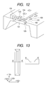
- Fig. 12 is a diagram schematically illustrating a liquid discharge head in the related art.
- Fig. 13 is a diagram schematically illustrating a common liquid chamber which is typically formed in a liquid discharge head.
- Fig. 1 is a diagram schematically illustrating the liquid discharge head manufactured according to the invention when it is viewed from the discharge surface side.
- Fig. 2 illustrates a perspective view illustrating the cross section of the liquid discharge head taken along the line A-A' in Fig. 1 .
- the liquid discharge energy generating elements 101 are provided on the Si substrate 100 having the ⁇ 100 ⁇ plane on its surface. Further, the discharge ports 103 for discharging the liquid and the flow paths 104 for holding the liquid are formed using a nozzle material 102. In addition, the plural supply ports 105 connected to the flow paths 104 are formed in the Si substrate 100.
- Figs. 3A to 3C is a diagram schematically illustrating the cross sections (figures in the left side) taken along the line A-A' and the cross sections (figures in the left side) of the liquid discharge head taken along the line B-B' in Fig. 1 which are illustrated in the order of processes.
- the substrate 300 is prepared (see Fig. 3A ).
- the liquid discharge energy generating elements 101 are provided on the Si substrate 100 having the ⁇ 100 ⁇ plane, and the discharge ports 103 and the flow paths 104 are formed.
- a passivation film 301 is provided in the substrate 300.
- the passivation film 301 is a film formed by a process for manufacturing transistors for driving the liquid discharge energy generating elements 101.
- the passivation film 301 is formed of a silicon oxide film, a silicon nitride film, or their laminated structure.
- the passivation film 301 may be formed all over the surface of the Si substrate 100, or may be formed in a structure in which some portions are partially removed.
- the discharge ports 103 and the flow paths 104 in the substrate 300 may be manufactured by the method according to the related art. At this time, the chips are aligned such that the longitudinal direction of the discharge port array is in the ⁇ 100> direction on the Si substrate 100 of the ⁇ 100 ⁇ plane as illustrated in Fig. 4 .
- guide holes 302 are formed using a laser beam such that the Si substrate 100 is removed from the rear surface of the Si substrate (the surface opposite to the surface on which the flow paths 104 are formed) (see Fig. 3B ), the first Si removal process). At this time, the guide holes 302 are formed as concave portions such that the two nearest guide holes 302 are aligned in the ⁇ 100> direction of the crystal axis on the Si substrate 100.
- the depth to be formed by the laser process there is a need to control the depth to be formed by the laser process so as not to reach the passivation film 301. This is because when the laser process reaches the passivation film 301, the passivation film 301 and the nozzle material 102 formed thereon may be damaged in some cases. Further, the value of the processed depth is determined in consideration of deviations in depth formed by the laser process.
- the interval between the tip end of the guide hole 302 as the concave portion and the passivation film 301 is suitably 5 ⁇ m or more from the point of view of preventing damage to the nozzle material 102 in the laser process.
- the laser beam used in the laser process is not particularly limited in its wavelength, the pulse time, and the spot shape of the laser irradiation as long as the Si substrate can be effectively removed.
- the spot shape of the laser irradiation is generally a circular shape, which is preferable in terms of cost.
- the diameter of the guide hole 302 to be formed is suitably in a range from 15 ⁇ m to 35 ⁇ m.
- the width of the Si pillar between the two nearest guide holes 302 is suitably in a range from 50 ⁇ m to 70 ⁇ m. This is because the supply ports can be formed at high density by a second Si removal process which will be describe later, and the strength of the liquid discharge head to be obtained can be enhanced.
- etching liquid based on tetra methyl ammonium hydroxide (TMAH)
- TMAH tetra methyl ammonium hydroxide
- the etching is carried out under the condition that the etching rate of the ⁇ 100 ⁇ plane is smaller than the etching rate of the ⁇ 110 ⁇ plane.
- This condition of the etching rate can be satisfied by properly adjusting various parameters such as TMAH concentration or humidity.
- TMAH concentration is in a range from 17.5% to 25% and the etching humidity is in a range from 70°C to 90°C
- the condition of the etching rate can be suitably satisfied.
- the etchant of the Si-crystal axis anisotropic etching is not limited to the TMAH solution.
- the etchant is not limited as long as the etchant has the etching rate of a crystal plane which satisfies the etching rate of the ⁇ 100 ⁇ plane is smaller than the etching rate of the ⁇ 110 ⁇ plane.
- the passivation film 301 is removed from the rear surface by chemical etching or by wet etching so as to form the independent supply ports 105 which are connected to the flow paths 104 (see Fig. 3C ).
- Figs. 5A to 5C are diagrams schematically illustrating liquid discharge head when it is viewed from the rear surface of the substrate.
- the discharge ports and the flow paths formed on the surface of the substrate are illustrated with a dotted line.
- the laser process is carried out on positions the Si substrate to which the flow paths formed on the surface can be connected from the rear surface, so that the guide holes 302 are formed.
- the two nearest guide holes are formed to be aligned in the ⁇ 100> direction with respect to the Si-crystal axis.
- the Si-crystal axis anisotropic etching is carried out under the condition that the etching rate of the ⁇ 100 ⁇ plane is smaller than the etching rate of the ⁇ 110 ⁇ plane.
- the ⁇ 100 ⁇ plane with a low etching rate is formed as the side surface of the independent supply port 105.
- the distance between the independent supply ports 105 may be disposed to be defined in the ⁇ 100> direction.
- the center positions of two guide holes 302 may deviate from the ⁇ 100> axis.
- the width of the Si pillar between the supply ports can be expressed as W1 or W2 illustrated in Fig. 3C .
- the width W1 or W2 of the Si pillar is determined by a distance of the ⁇ 100 ⁇ plane which is generated by the crystal axis anisotropic etching.
- the pitch of the array of the discharge ports 103 is typically narrowed with respect to the longitudinal direction so that W1 is smaller than W2.
- lines may be formed to electrically connect the liquid discharge energy generating elements 101 and the semiconductor elements for driving the liquid discharge energy generating elements 101 in some cases.
- the Si pillar plays a central role in transferring the heat generated from the liquid discharge energy generating elements 101 to the substrate.
- W1 is suitable for W1 to be stably formed to have a value which is as large as possible.
- W1 is in a range from 35 ⁇ m to 50 ⁇ m, which is suitable because the discharge ports 103 can be formed at high density and the strength and the stability of the liquid discharge head are high.
- both the processed surface in the depth direction and the processed surface in the horizontal direction are the ⁇ 100 ⁇ plane, these processed surfaces are hardly influenced by the change in etching rate caused by concentration of the etchant, humidity, and impurities. Therefore, an effect can be obtained such that it is easy to stability form the structure of the supply ports.
- the printing quality can be favorably obtained by the liquid discharge head which can be manufactured with good yield.
- FIGS. 6A to 6C are diagrams schematically illustrating the cross sections (figures in the left side) taken along the line A-A' and the cross sections (figures in the right side) taken along the line B-B' in Fig. 1 in the order of processes.
- the substrate 600 provided with a sacrificial layer 601 is prepared (see Fig. 6A ).
- the sacrificial layer 601 is provided by being isotropically etched when the Si-crystal axis anisotropic etching is carried out.
- the sacrificial layer 601 is patterned with a desired size.
- a metal film such as, for example, aluminum, a polycrystalline Si film, or a porous Si oxide film can be employed.
- the guide holes 602 are formed from the rear surface of the substrate (see Fig. 6B ).
- the laser process or the dry etching may be employed. In this embodiment, the processing example carried out by the dry etching will be described.
- the guide holes 602 may be formed to reach the sacrificial layer 601 or the passivation film.
- the electrically conductive sacrificial layer it can be expected that a shape defect caused by the charged-up substrate when the Si substrate is subjected to the etching process is effectively suppressed.
- the guide holes 602 are formed using a photolithography technique such that the two nearest guide holes 602 are aligned in the ⁇ 100> direction of the Si-crystal axis.
- the cross-sectional shape of the guide hole 602 when it is viewed in parallel to the surface of the substrate is not limited to a circular shape or a rectangular shape as long as the area of the cross section falls within a range of the sacrificial layer 601 which is patterned on the substrate side in which the flow paths are formed.
- the Si-crystal axis anisotropic etching is carried out.
- the sacrificial layer 601 is also removed at the same time.
- the passivation film is removed from the rear surface by chemical etching or dry etching so as to form the independent supply ports which are connected to the flow paths (see Fig. 6C ).
- the space is formed as a part of the supply ports.
- the ends of the supply ports on the substrate surface side are defined by the patterning shape of the sacrificial layer 601. For this reason, by using the sacrificial layer 601, the positions of the openings of the supply ports on the substrate surface side can be efficiently formed with high accuracy.
- the shape of the cross section of the independent supply port in the vertical direction with respect to the substrate surface differs according to a large number of the parameters such as the conditions of the crystal anisotropic etching, the pattern of the sacrificial layer 601, and the etching rate of the sacrificial layer 601, but the invention is not limited to these shapes.
- FIGS. 7A to 7C are diagrams schematically illustrating the cross sections (figures in the left side) taken along the line A-A' and the cross sections (figures in the right side) taken along the line B-B' in Fig. 8B .
- the substrate is prepared.
- the substrate may be provided with the sacrificial layer or not.
- the etching resist layer 700 is patterned on the rear surface of the substrate so as to correspond to the position of the space 701 which becomes the common liquid chamber ( Fig. 7A ). Thereafter, the Si substrate is removed by etching so as to form the space 701 which becomes the common liquid chamber.
- the Si-crystal axis anisotropic etching or the dry etching may be employed as an etching method of forming the space 701 which becomes the common liquid chamber.
- the etching resist layer 700 can be formed by properly selecting a material which is suitable to the selected etching method.
- the space 701 as the common liquid chamber can have high perpendicularity and shrinkage in chip can be realized.
- the arrangement can be performed regardless of the Si crystal axis. Therefore, flexibility in design can be increased. There is an advantage in that the flexibility in design can be increased.
- the Si substrate may be prepared in arrangement of Fig. 4 .
- the longitudinal direction of the array of the discharge ports is limited to the ⁇ 110> direction due to the angle of the ⁇ 111 ⁇ plane which is exposed by the Si-crystal axis anisotropic etching. Therefore, for example, as illustrated in Figs. 8A to 8B , the discharge ports, the flow paths, and the independent supply ports may be obliquely aligned on the region 702 which is formed thin in the substrate.
- the independent supply ports are formed on the region 702 which is formed so as to be thin in the substrate (see Figs. 7B and 7C ) similarly to Embodiment 1 and Embodiment 2. Therefore, the space 701 is formed as the common liquid chamber in which at least two or more independent supply ports are connected. Since the independent supply ports are short in its depth direction, the aspect ratio of the processed shape is small when the guide holes are processed, and the accuracy of the processed shape or the tact performance is effectively increased.
- Figs. 10A to 10F illustrate a method of manufacturing the liquid discharge head of this example.
- the Si substrate was prepared which included the ⁇ 100 ⁇ plane and was provided with a heater for discharging the liquid and a semiconductor element for driving and controlling the heater (see Fig. 10A ).
- a polyether amide 700 using N-methyl-pyrrolidone as a solvent was formed as a film on the rear surface of a wafer by spin coating, and a positive resist was further coated on the rear surface of the wafer. After the positive resist was patterned on the rear surface of the wafer using the photolithography technique, chemical dry etching was performed to remove a portion of the polyether amide layer and then the positive resist was peeled off (see Fig. 10B ).
- a resist was coated which containing poly methyl isopropenyl ketone and served as a mold material 1001 for forming an ink flow path, and then exposure and development were carried out followed by the patterning ( Fig. 10C ).
- a photosensitive epoxy 102 was coated to form an orifice plate, and then patterned by exposure and development so as to form the discharge port (see Fig. 10D ).
- a protective film 1002 made of a rubber resin was coated on the wafer surface and the peripheral portion.
- the crystal axis anisotropic etching was carried out such that the remaining film thickness of the substrate was 125 ⁇ m, so that the space which became the common liquid chamber was formed.
- TMAH tetra methyl ammonium hydroxide
- the two nearest guide holes were formed such that the guide holes were aligned in the ⁇ 100> direction of the Si crystal axis.
- the wavelength of the laser beam was 355 nm
- the pulse time was 70 ⁇ 5 ns
- the spot shape of the laser irradiation was a circle.
- the depth of the formed guide hole was 120 ⁇ m
- the distance between the tip end of the guide hole and the passivation film was 5 ⁇ m.
- the width of the Si pillar between the two nearest guide holes was 59 ⁇ m (see Fig. 10E ).
- the crystal axis anisotropic etching was carried out on the guide hole so as to form the supply port in which the ⁇ 100 ⁇ plane became a wall surface.
- the supply port was formed so as to reach the passivation film.
- the polyether amide resin of the rear surface of the wafer was removed by chemical dry etching.
- the passivation layer was removed by chemical dry etching.
- the protective film 1002 coated on the wafer surface and the peripheral portion of the wafer was removed by using xylene.
- the resist as the mold material 1001 of the ink flow path was removed by using methyl lactate (see Fig. 10F ).
- the liquid discharge head provided with the independent supply port and the sub flow path was manufactured.
- the width of the Si pillar between the two nearest supply ports of the obtained liquid discharge head was 39 ⁇ m, and sufficient strength was exhibited.
- the widths of the respective Si pillars were substantially equal to each other, and there were hardly any deviations found.
- Figs. 11A to 11C illustrate a method of manufacturing the liquid discharge head of this example.
- the Si substrate was prepared which included the ⁇ 100 ⁇ plane and was provided with a heater for discharging the liquid, a semiconductor element for driving and controlling the heater, and an Al film which is the sacrificial layer of the Si-crystal axis anisotropic etching.
- the chips of the liquid discharge head were disposed with respect to the crystal orientation of the Si wafer as illustrated in Fig. 4 .
- the discharge ports were formed in the same processes as those in Example 1 (see Fig. 11A ). Thereafter, in order to protect the formed orifice plate, a protective film made of a rubber resin was coated on the wafer surface and the peripheral portion.
- the space was formed as the common liquid chamber by the dry etching in the Bosch manner such that the substrate had a film thickness of 125 ⁇ m.
- the positive resist was coated on the bottom portion of the space formed as the common liquid chamber by a spray manner.
- the positive resist was patterned using the photolithography manner such that the two nearest guide holes were aligned in the ⁇ 100> direction of the Si crystal axis, and then subjected to the dry etching n the Bosch manner so as to form the guide holes.
- Al as the sacrificial layer was used as an etching stopper.
- the shape of the formed guide hole was a circle, and the area thereof fell within the range of the sacrificial layer.
- the width of the Si pillar between the two nearest guide holes was 59 ⁇ m (see Fig. 11B ).
- the crystal axis anisotropic etching was carried out on the guide hole and the sacrificial layer was removed so as to form the supply port of which the side surface is in the ⁇ 100 ⁇ plane.
- the etching rate of the ⁇ 100 ⁇ plane at this time was 0.64 ⁇ m/min, and the etching rate of the ⁇ 110 ⁇ plane was 1.30 ⁇ m/min.
- the polyether amide resin of the rear surface of the wafer was removed by chemical dry etching.
- the passivation layer was removed by chemical dry etching.
- the protective film coated on the wafer surface and the peripheral portion of the wafer was removed by using xylene.
- the resist as the mold material 1001 of the ink flow path was removed by using methyl lactate (see Fig. 11C ).
- the liquid discharge head was manufactured.
- the width of the Si pillar between the two nearest supply ports of the obtained liquid discharge head was 39 ⁇ m, and a sufficient strength was exhibited.
- the widths of the respective Si pillars were substantially equal to each other, and there were hardly any deviations found.
- a liquid discharge head includes an Si substrate which is provided with an element for generating energy used in discharging a liquid and a liquid supply port which is provided to pass through the Si substrate from first surface to rear surface so as to supply a liquid to the element.
- a method of manufacturing the substrate includes: forming a plurality of concave portions on the rear surface of the Si substrate of which a plane orientation is ⁇ 100 ⁇ , the concave portions facing the first surface and aligned in rows along a ⁇ 100> direction the first surface; and forming a plurality of the supply ports by carrying out a crystal axis anisotropic etching on the Si substrate through the concave portions using an etching liquid of which an etching rate of the ⁇ 100 ⁇ plane of the Si substrate is slower than that of the ⁇ 110 ⁇ plane of the Si substrate.
Landscapes
- Engineering & Computer Science (AREA)
- Manufacturing & Machinery (AREA)
- Chemical & Material Sciences (AREA)
- Physics & Mathematics (AREA)
- Chemical Kinetics & Catalysis (AREA)
- Geometry (AREA)
- Optics & Photonics (AREA)
- General Chemical & Material Sciences (AREA)
- Materials Engineering (AREA)
- Mechanical Engineering (AREA)
- Metallurgy (AREA)
- Organic Chemistry (AREA)
- Particle Formation And Scattering Control In Inkjet Printers (AREA)
- Weting (AREA)
Applications Claiming Priority (1)
| Application Number | Priority Date | Filing Date | Title |
|---|---|---|---|
| JP2008323787A JP4656670B2 (ja) | 2008-12-19 | 2008-12-19 | 液体吐出ヘッド及び液体吐出ヘッドの製造方法 |
Publications (3)
| Publication Number | Publication Date |
|---|---|
| EP2202076A2 true EP2202076A2 (de) | 2010-06-30 |
| EP2202076A3 EP2202076A3 (de) | 2012-11-21 |
| EP2202076B1 EP2202076B1 (de) | 2015-07-29 |
Family
ID=42101600
Family Applications (1)
| Application Number | Title | Priority Date | Filing Date |
|---|---|---|---|
| EP09178533.7A Not-in-force EP2202076B1 (de) | 2008-12-19 | 2009-12-09 | Flüssigkeitsausstoßkopf und Verfahren zur Herstellung des Flüssigkeitsausstoßkopfs |
Country Status (6)
| Country | Link |
|---|---|
| US (1) | US8366951B2 (de) |
| EP (1) | EP2202076B1 (de) |
| JP (1) | JP4656670B2 (de) |
| KR (1) | KR101248344B1 (de) |
| CN (1) | CN101746143B (de) |
| RU (1) | RU2416522C1 (de) |
Cited By (2)
| Publication number | Priority date | Publication date | Assignee | Title |
|---|---|---|---|---|
| WO2013048742A1 (en) * | 2011-09-30 | 2013-04-04 | Eastman Kodak Company | Liquid ejection device with planarized nozzle plate |
| EP3351390A1 (de) * | 2016-12-27 | 2018-07-25 | Seiko Epson Corporation | Verfahren zur herstellung eines flüssigkeitsausstosskopfes |
Families Citing this family (10)
| Publication number | Priority date | Publication date | Assignee | Title |
|---|---|---|---|---|
| US8435805B2 (en) * | 2010-09-06 | 2013-05-07 | Canon Kabushiki Kaisha | Method of manufacturing a substrate for liquid ejection head |
| JP5744549B2 (ja) * | 2011-02-02 | 2015-07-08 | キヤノン株式会社 | インクジェット記録ヘッドおよびインクジェット記録ヘッドの製造方法 |
| JP5539547B2 (ja) * | 2012-01-24 | 2014-07-02 | キヤノン株式会社 | 液体吐出ヘッド及びその製造方法 |
| JP5925064B2 (ja) * | 2012-06-20 | 2016-05-25 | キヤノン株式会社 | 液体吐出ヘッドの製造方法 |
| JP5980012B2 (ja) * | 2012-06-27 | 2016-08-31 | キヤノン株式会社 | シリコンウェハの加工方法 |
| JP6034207B2 (ja) * | 2013-01-28 | 2016-11-30 | 京セラ株式会社 | 液体吐出ヘッド、および記録装置 |
| JP2015168143A (ja) * | 2014-03-06 | 2015-09-28 | セイコーエプソン株式会社 | 貫通孔の形成方法、部材、インクジェットヘッド、インクジェットヘッドユニットおよびインクジェット式記録装置 |
| JP6504938B2 (ja) * | 2015-06-25 | 2019-04-24 | キヤノン株式会社 | 液体吐出ヘッド用基板および液体吐出ヘッド |
| JP2018094845A (ja) | 2016-12-15 | 2018-06-21 | キヤノン株式会社 | 液体吐出ヘッド |
| JP2019089233A (ja) * | 2017-11-14 | 2019-06-13 | エスアイアイ・プリンテック株式会社 | 噴射孔プレートの製造方法 |
Citations (5)
| Publication number | Priority date | Publication date | Assignee | Title |
|---|---|---|---|---|
| EP0609012A2 (de) | 1993-01-25 | 1994-08-03 | Hewlett-Packard Company | Verfahren zum Herstellen eines thermischen Farbstrahldruckkopfs |
| US6137510A (en) | 1996-11-15 | 2000-10-24 | Canon Kabushiki Kaisha | Ink jet head |
| US20060094200A1 (en) | 2004-10-29 | 2006-05-04 | Leith Steven D | Methods for controlling feature dimensions in crystalline substrates |
| JP2007210242A (ja) | 2006-02-10 | 2007-08-23 | Canon Inc | インクジェット記録ヘッド及びその作製方法 |
| JP2008260151A (ja) | 2007-04-10 | 2008-10-30 | Canon Inc | インクジェットヘッドおよびマイクロ構造体の作製方法 |
Family Cites Families (7)
| Publication number | Priority date | Publication date | Assignee | Title |
|---|---|---|---|---|
| US6386686B1 (en) | 1998-12-03 | 2002-05-14 | Canon Kabushiki Kaisha | Liquid discharge head, manufacturing method of liquid discharge head, head cartridge, and liquid discharge apparatus |
| JP2001010047A (ja) * | 1999-06-29 | 2001-01-16 | Ricoh Co Ltd | インクジェットヘッド及びその製造方法 |
| JP2001018385A (ja) * | 1999-07-09 | 2001-01-23 | Ricoh Co Ltd | インクジェットヘッド |
| JP4217434B2 (ja) * | 2002-07-04 | 2009-02-04 | キヤノン株式会社 | スルーホールの形成方法及びこれを用いたインクジェットヘッド |
| JP4537246B2 (ja) | 2004-05-06 | 2010-09-01 | キヤノン株式会社 | インクジェット記録ヘッド用基体の製造方法及び該方法により製造された前記基体を用いた記録ヘッドの製造方法 |
| JP4447974B2 (ja) | 2004-06-28 | 2010-04-07 | キヤノン株式会社 | インクジェットヘッドの製造方法 |
| US7326356B2 (en) | 2004-08-31 | 2008-02-05 | Hewlett-Packard Development Company, L.P. | Substrate and method of forming substrate for fluid ejection device |
-
2008
- 2008-12-19 JP JP2008323787A patent/JP4656670B2/ja not_active Expired - Fee Related
-
2009
- 2009-12-02 US US12/629,238 patent/US8366951B2/en not_active Expired - Fee Related
- 2009-12-09 EP EP09178533.7A patent/EP2202076B1/de not_active Not-in-force
- 2009-12-14 KR KR1020090123747A patent/KR101248344B1/ko not_active Expired - Fee Related
- 2009-12-18 CN CN2009102594215A patent/CN101746143B/zh not_active Expired - Fee Related
- 2009-12-18 RU RU2009147227/12A patent/RU2416522C1/ru not_active IP Right Cessation
Patent Citations (5)
| Publication number | Priority date | Publication date | Assignee | Title |
|---|---|---|---|---|
| EP0609012A2 (de) | 1993-01-25 | 1994-08-03 | Hewlett-Packard Company | Verfahren zum Herstellen eines thermischen Farbstrahldruckkopfs |
| US6137510A (en) | 1996-11-15 | 2000-10-24 | Canon Kabushiki Kaisha | Ink jet head |
| US20060094200A1 (en) | 2004-10-29 | 2006-05-04 | Leith Steven D | Methods for controlling feature dimensions in crystalline substrates |
| JP2007210242A (ja) | 2006-02-10 | 2007-08-23 | Canon Inc | インクジェット記録ヘッド及びその作製方法 |
| JP2008260151A (ja) | 2007-04-10 | 2008-10-30 | Canon Inc | インクジェットヘッドおよびマイクロ構造体の作製方法 |
Cited By (2)
| Publication number | Priority date | Publication date | Assignee | Title |
|---|---|---|---|---|
| WO2013048742A1 (en) * | 2011-09-30 | 2013-04-04 | Eastman Kodak Company | Liquid ejection device with planarized nozzle plate |
| EP3351390A1 (de) * | 2016-12-27 | 2018-07-25 | Seiko Epson Corporation | Verfahren zur herstellung eines flüssigkeitsausstosskopfes |
Also Published As
| Publication number | Publication date |
|---|---|
| KR20100071912A (ko) | 2010-06-29 |
| JP4656670B2 (ja) | 2011-03-23 |
| US20100156990A1 (en) | 2010-06-24 |
| EP2202076A3 (de) | 2012-11-21 |
| KR101248344B1 (ko) | 2013-04-01 |
| CN101746143A (zh) | 2010-06-23 |
| US8366951B2 (en) | 2013-02-05 |
| RU2416522C1 (ru) | 2011-04-20 |
| JP2010143119A (ja) | 2010-07-01 |
| EP2202076B1 (de) | 2015-07-29 |
| CN101746143B (zh) | 2013-05-01 |
Similar Documents
| Publication | Publication Date | Title |
|---|---|---|
| US8366951B2 (en) | Liquid discharge head and method of manufacturing a substrate for the liquid discharge head | |
| KR100397604B1 (ko) | 버블 젯 방식의 잉크 젯 프린트 헤드 및 그 제조방법 | |
| US6019907A (en) | Forming refill for monolithic inkjet printhead | |
| KR100468859B1 (ko) | 일체형 잉크젯 프린트헤드 및 그 제조방법 | |
| CN105102230B (zh) | 流体喷射装置 | |
| KR100552660B1 (ko) | 버블 젯 방식의 잉크 젯 프린트 헤드 | |
| KR100374788B1 (ko) | 버블 젯 방식의 잉크 젯 프린트 헤드, 그 제조방법 및잉크 토출방법 | |
| KR100493160B1 (ko) | 테이퍼 형상의 노즐을 가진 일체형 잉크젯 프린트헤드 및그 제조방법 | |
| KR100408268B1 (ko) | 버블 젯 방식의 잉크 젯 프린트 헤드 및 그 제조방법 | |
| KR100433530B1 (ko) | 일체형 잉크젯 프린트 헤드의 제조 방법 | |
| US9096063B2 (en) | Liquid ejection head and method of manufacturing same | |
| JP4979793B2 (ja) | 液体吐出ヘッド用基板の製造方法 | |
| TW201348010A (zh) | 具有凹入式槽縫末端的列印頭 | |
| US9205654B2 (en) | Method of manufacturing a liquid ejection head | |
| KR100421216B1 (ko) | 버블젯 방식의 잉크젯 프린트 헤드 및 그 제작방법 | |
| US20070019036A1 (en) | Inkjet head and manufacturing method thereof | |
| JP4261904B2 (ja) | インクジェット記録ヘッド用基板の製造方法、およびインクジェット記録ヘッドの製造方法 | |
| KR100641359B1 (ko) | 고효율 히터를 갖는 잉크젯 프린트 헤드 및 그 제조 방법 | |
| KR20050013856A (ko) | 잉크젯 프린트헤드 및 그 제조방법 | |
| JP4704179B2 (ja) | インクジェットヘッドおよびインクジェットヘッドの製造方法 | |
| JPWO2006062092A1 (ja) | インクジェットヘッドおよびインクジェットヘッドの製造方法 | |
| JP2006224592A (ja) | インクジェット記録ヘッドおよびインクジェット記録ヘッド用Si基板 |
Legal Events
| Date | Code | Title | Description |
|---|---|---|---|
| PUAI | Public reference made under article 153(3) epc to a published international application that has entered the european phase |
Free format text: ORIGINAL CODE: 0009012 |
|
| AK | Designated contracting states |
Kind code of ref document: A2 Designated state(s): AT BE BG CH CY CZ DE DK EE ES FI FR GB GR HR HU IE IS IT LI LT LU LV MC MK MT NL NO PL PT RO SE SI SK SM TR |
|
| AX | Request for extension of the european patent |
Extension state: AL BA RS |
|
| PUAL | Search report despatched |
Free format text: ORIGINAL CODE: 0009013 |
|
| AK | Designated contracting states |
Kind code of ref document: A3 Designated state(s): AT BE BG CH CY CZ DE DK EE ES FI FR GB GR HR HU IE IS IT LI LT LU LV MC MK MT NL NO PL PT RO SE SI SK SM TR |
|
| AX | Request for extension of the european patent |
Extension state: AL BA RS |
|
| RIC1 | Information provided on ipc code assigned before grant |
Ipc: B41J 2/14 20060101AFI20121016BHEP Ipc: B41J 2/16 20060101ALI20121016BHEP |
|
| 17P | Request for examination filed |
Effective date: 20130521 |
|
| 17Q | First examination report despatched |
Effective date: 20130626 |
|
| GRAP | Despatch of communication of intention to grant a patent |
Free format text: ORIGINAL CODE: EPIDOSNIGR1 |
|
| INTG | Intention to grant announced |
Effective date: 20150211 |
|
| GRAS | Grant fee paid |
Free format text: ORIGINAL CODE: EPIDOSNIGR3 |
|
| GRAA | (expected) grant |
Free format text: ORIGINAL CODE: 0009210 |
|
| AK | Designated contracting states |
Kind code of ref document: B1 Designated state(s): AT BE BG CH CY CZ DE DK EE ES FI FR GB GR HR HU IE IS IT LI LT LU LV MC MK MT NL NO PL PT RO SE SI SK SM TR |
|
| REG | Reference to a national code |
Ref country code: GB Ref legal event code: FG4D |
|
| REG | Reference to a national code |
Ref country code: CH Ref legal event code: EP |
|
| REG | Reference to a national code |
Ref country code: AT Ref legal event code: REF Ref document number: 738947 Country of ref document: AT Kind code of ref document: T Effective date: 20150815 |
|
| REG | Reference to a national code |
Ref country code: IE Ref legal event code: FG4D |
|
| REG | Reference to a national code |
Ref country code: DE Ref legal event code: R096 Ref document number: 602009032454 Country of ref document: DE |
|
| REG | Reference to a national code |
Ref country code: AT Ref legal event code: MK05 Ref document number: 738947 Country of ref document: AT Kind code of ref document: T Effective date: 20150729 |
|
| REG | Reference to a national code |
Ref country code: LT Ref legal event code: MG4D |
|
| REG | Reference to a national code |
Ref country code: NL Ref legal event code: MP Effective date: 20150729 |
|
| PG25 | Lapsed in a contracting state [announced via postgrant information from national office to epo] |
Ref country code: NO Free format text: LAPSE BECAUSE OF FAILURE TO SUBMIT A TRANSLATION OF THE DESCRIPTION OR TO PAY THE FEE WITHIN THE PRESCRIBED TIME-LIMIT Effective date: 20151029 Ref country code: LT Free format text: LAPSE BECAUSE OF FAILURE TO SUBMIT A TRANSLATION OF THE DESCRIPTION OR TO PAY THE FEE WITHIN THE PRESCRIBED TIME-LIMIT Effective date: 20150729 Ref country code: LV Free format text: LAPSE BECAUSE OF FAILURE TO SUBMIT A TRANSLATION OF THE DESCRIPTION OR TO PAY THE FEE WITHIN THE PRESCRIBED TIME-LIMIT Effective date: 20150729 Ref country code: FI Free format text: LAPSE BECAUSE OF FAILURE TO SUBMIT A TRANSLATION OF THE DESCRIPTION OR TO PAY THE FEE WITHIN THE PRESCRIBED TIME-LIMIT Effective date: 20150729 Ref country code: GR Free format text: LAPSE BECAUSE OF FAILURE TO SUBMIT A TRANSLATION OF THE DESCRIPTION OR TO PAY THE FEE WITHIN THE PRESCRIBED TIME-LIMIT Effective date: 20151030 |
|
| PG25 | Lapsed in a contracting state [announced via postgrant information from national office to epo] |
Ref country code: IS Free format text: LAPSE BECAUSE OF FAILURE TO SUBMIT A TRANSLATION OF THE DESCRIPTION OR TO PAY THE FEE WITHIN THE PRESCRIBED TIME-LIMIT Effective date: 20151129 Ref country code: PL Free format text: LAPSE BECAUSE OF FAILURE TO SUBMIT A TRANSLATION OF THE DESCRIPTION OR TO PAY THE FEE WITHIN THE PRESCRIBED TIME-LIMIT Effective date: 20150729 Ref country code: PT Free format text: LAPSE BECAUSE OF FAILURE TO SUBMIT A TRANSLATION OF THE DESCRIPTION OR TO PAY THE FEE WITHIN THE PRESCRIBED TIME-LIMIT Effective date: 20151130 Ref country code: ES Free format text: LAPSE BECAUSE OF FAILURE TO SUBMIT A TRANSLATION OF THE DESCRIPTION OR TO PAY THE FEE WITHIN THE PRESCRIBED TIME-LIMIT Effective date: 20150729 Ref country code: HR Free format text: LAPSE BECAUSE OF FAILURE TO SUBMIT A TRANSLATION OF THE DESCRIPTION OR TO PAY THE FEE WITHIN THE PRESCRIBED TIME-LIMIT Effective date: 20150729 Ref country code: AT Free format text: LAPSE BECAUSE OF FAILURE TO SUBMIT A TRANSLATION OF THE DESCRIPTION OR TO PAY THE FEE WITHIN THE PRESCRIBED TIME-LIMIT Effective date: 20150729 Ref country code: SE Free format text: LAPSE BECAUSE OF FAILURE TO SUBMIT A TRANSLATION OF THE DESCRIPTION OR TO PAY THE FEE WITHIN THE PRESCRIBED TIME-LIMIT Effective date: 20150729 |
|
| PG25 | Lapsed in a contracting state [announced via postgrant information from national office to epo] |
Ref country code: NL Free format text: LAPSE BECAUSE OF FAILURE TO SUBMIT A TRANSLATION OF THE DESCRIPTION OR TO PAY THE FEE WITHIN THE PRESCRIBED TIME-LIMIT Effective date: 20150729 |
|
| PG25 | Lapsed in a contracting state [announced via postgrant information from national office to epo] |
Ref country code: DK Free format text: LAPSE BECAUSE OF FAILURE TO SUBMIT A TRANSLATION OF THE DESCRIPTION OR TO PAY THE FEE WITHIN THE PRESCRIBED TIME-LIMIT Effective date: 20150729 Ref country code: SK Free format text: LAPSE BECAUSE OF FAILURE TO SUBMIT A TRANSLATION OF THE DESCRIPTION OR TO PAY THE FEE WITHIN THE PRESCRIBED TIME-LIMIT Effective date: 20150729 Ref country code: CZ Free format text: LAPSE BECAUSE OF FAILURE TO SUBMIT A TRANSLATION OF THE DESCRIPTION OR TO PAY THE FEE WITHIN THE PRESCRIBED TIME-LIMIT Effective date: 20150729 Ref country code: IT Free format text: LAPSE BECAUSE OF FAILURE TO SUBMIT A TRANSLATION OF THE DESCRIPTION OR TO PAY THE FEE WITHIN THE PRESCRIBED TIME-LIMIT Effective date: 20150729 Ref country code: EE Free format text: LAPSE BECAUSE OF FAILURE TO SUBMIT A TRANSLATION OF THE DESCRIPTION OR TO PAY THE FEE WITHIN THE PRESCRIBED TIME-LIMIT Effective date: 20150729 |
|
| REG | Reference to a national code |
Ref country code: DE Ref legal event code: R097 Ref document number: 602009032454 Country of ref document: DE |
|
| PG25 | Lapsed in a contracting state [announced via postgrant information from national office to epo] |
Ref country code: RO Free format text: LAPSE BECAUSE OF FAILURE TO SUBMIT A TRANSLATION OF THE DESCRIPTION OR TO PAY THE FEE WITHIN THE PRESCRIBED TIME-LIMIT Effective date: 20150729 Ref country code: BE Free format text: LAPSE BECAUSE OF NON-PAYMENT OF DUE FEES Effective date: 20151231 |
|
| PLBE | No opposition filed within time limit |
Free format text: ORIGINAL CODE: 0009261 |
|
| STAA | Information on the status of an ep patent application or granted ep patent |
Free format text: STATUS: NO OPPOSITION FILED WITHIN TIME LIMIT |
|
| 26N | No opposition filed |
Effective date: 20160502 |
|
| PG25 | Lapsed in a contracting state [announced via postgrant information from national office to epo] |
Ref country code: MC Free format text: LAPSE BECAUSE OF FAILURE TO SUBMIT A TRANSLATION OF THE DESCRIPTION OR TO PAY THE FEE WITHIN THE PRESCRIBED TIME-LIMIT Effective date: 20150729 Ref country code: LU Free format text: LAPSE BECAUSE OF FAILURE TO SUBMIT A TRANSLATION OF THE DESCRIPTION OR TO PAY THE FEE WITHIN THE PRESCRIBED TIME-LIMIT Effective date: 20151209 |
|
| REG | Reference to a national code |
Ref country code: CH Ref legal event code: PL |
|
| PG25 | Lapsed in a contracting state [announced via postgrant information from national office to epo] |
Ref country code: SI Free format text: LAPSE BECAUSE OF FAILURE TO SUBMIT A TRANSLATION OF THE DESCRIPTION OR TO PAY THE FEE WITHIN THE PRESCRIBED TIME-LIMIT Effective date: 20150729 |
|
| REG | Reference to a national code |
Ref country code: IE Ref legal event code: MM4A |
|
| REG | Reference to a national code |
Ref country code: FR Ref legal event code: ST Effective date: 20160831 |
|
| PG25 | Lapsed in a contracting state [announced via postgrant information from national office to epo] |
Ref country code: CH Free format text: LAPSE BECAUSE OF NON-PAYMENT OF DUE FEES Effective date: 20151231 Ref country code: IE Free format text: LAPSE BECAUSE OF NON-PAYMENT OF DUE FEES Effective date: 20151209 Ref country code: LI Free format text: LAPSE BECAUSE OF NON-PAYMENT OF DUE FEES Effective date: 20151231 |
|
| PG25 | Lapsed in a contracting state [announced via postgrant information from national office to epo] |
Ref country code: FR Free format text: LAPSE BECAUSE OF NON-PAYMENT OF DUE FEES Effective date: 20151231 |
|
| PG25 | Lapsed in a contracting state [announced via postgrant information from national office to epo] |
Ref country code: BE Free format text: LAPSE BECAUSE OF FAILURE TO SUBMIT A TRANSLATION OF THE DESCRIPTION OR TO PAY THE FEE WITHIN THE PRESCRIBED TIME-LIMIT Effective date: 20150729 |
|
| PG25 | Lapsed in a contracting state [announced via postgrant information from national office to epo] |
Ref country code: HU Free format text: LAPSE BECAUSE OF FAILURE TO SUBMIT A TRANSLATION OF THE DESCRIPTION OR TO PAY THE FEE WITHIN THE PRESCRIBED TIME-LIMIT; INVALID AB INITIO Effective date: 20091209 Ref country code: SM Free format text: LAPSE BECAUSE OF FAILURE TO SUBMIT A TRANSLATION OF THE DESCRIPTION OR TO PAY THE FEE WITHIN THE PRESCRIBED TIME-LIMIT Effective date: 20150729 Ref country code: BG Free format text: LAPSE BECAUSE OF FAILURE TO SUBMIT A TRANSLATION OF THE DESCRIPTION OR TO PAY THE FEE WITHIN THE PRESCRIBED TIME-LIMIT Effective date: 20150729 |
|
| PG25 | Lapsed in a contracting state [announced via postgrant information from national office to epo] |
Ref country code: CY Free format text: LAPSE BECAUSE OF FAILURE TO SUBMIT A TRANSLATION OF THE DESCRIPTION OR TO PAY THE FEE WITHIN THE PRESCRIBED TIME-LIMIT Effective date: 20150729 |
|
| PG25 | Lapsed in a contracting state [announced via postgrant information from national office to epo] |
Ref country code: TR Free format text: LAPSE BECAUSE OF FAILURE TO SUBMIT A TRANSLATION OF THE DESCRIPTION OR TO PAY THE FEE WITHIN THE PRESCRIBED TIME-LIMIT Effective date: 20150729 Ref country code: MT Free format text: LAPSE BECAUSE OF FAILURE TO SUBMIT A TRANSLATION OF THE DESCRIPTION OR TO PAY THE FEE WITHIN THE PRESCRIBED TIME-LIMIT Effective date: 20150729 |
|
| PGFP | Annual fee paid to national office [announced via postgrant information from national office to epo] |
Ref country code: GB Payment date: 20171228 Year of fee payment: 9 |
|
| PGFP | Annual fee paid to national office [announced via postgrant information from national office to epo] |
Ref country code: DE Payment date: 20180228 Year of fee payment: 9 |
|
| PG25 | Lapsed in a contracting state [announced via postgrant information from national office to epo] |
Ref country code: MK Free format text: LAPSE BECAUSE OF FAILURE TO SUBMIT A TRANSLATION OF THE DESCRIPTION OR TO PAY THE FEE WITHIN THE PRESCRIBED TIME-LIMIT Effective date: 20150729 |
|
| REG | Reference to a national code |
Ref country code: DE Ref legal event code: R119 Ref document number: 602009032454 Country of ref document: DE |
|
| GBPC | Gb: european patent ceased through non-payment of renewal fee |
Effective date: 20181209 |
|
| PG25 | Lapsed in a contracting state [announced via postgrant information from national office to epo] |
Ref country code: DE Free format text: LAPSE BECAUSE OF NON-PAYMENT OF DUE FEES Effective date: 20190702 |
|
| PG25 | Lapsed in a contracting state [announced via postgrant information from national office to epo] |
Ref country code: GB Free format text: LAPSE BECAUSE OF NON-PAYMENT OF DUE FEES Effective date: 20181209 |