EP2242095B1 - Halbleiterbauelement und verfahren zu seiner herstellung - Google Patents
Halbleiterbauelement und verfahren zu seiner herstellung Download PDFInfo
- Publication number
- EP2242095B1 EP2242095B1 EP07860452.7A EP07860452A EP2242095B1 EP 2242095 B1 EP2242095 B1 EP 2242095B1 EP 07860452 A EP07860452 A EP 07860452A EP 2242095 B1 EP2242095 B1 EP 2242095B1
- Authority
- EP
- European Patent Office
- Prior art keywords
- external connection
- row
- disposed
- cells
- semiconductor device
- Prior art date
- Legal status (The legal status is an assumption and is not a legal conclusion. Google has not performed a legal analysis and makes no representation as to the accuracy of the status listed.)
- Active
Links
Images









Classifications
-
- H—ELECTRICITY
- H10—SEMICONDUCTOR DEVICES; ELECTRIC SOLID-STATE DEVICES NOT OTHERWISE PROVIDED FOR
- H10D—INORGANIC ELECTRIC SEMICONDUCTOR DEVICES
- H10D89/00—Aspects of integrated devices not covered by groups H10D84/00 - H10D88/00
-
- H—ELECTRICITY
- H10—SEMICONDUCTOR DEVICES; ELECTRIC SOLID-STATE DEVICES NOT OTHERWISE PROVIDED FOR
- H10P—GENERIC PROCESSES OR APPARATUS FOR THE MANUFACTURE OR TREATMENT OF DEVICES COVERED BY CLASS H10
- H10P74/00—Testing or measuring during manufacture or treatment of wafers, substrates or devices
- H10P74/27—Structural arrangements therefor
- H10P74/273—Interconnections for measuring or testing, e.g. probe pads
-
- H—ELECTRICITY
- H10—SEMICONDUCTOR DEVICES; ELECTRIC SOLID-STATE DEVICES NOT OTHERWISE PROVIDED FOR
- H10W—GENERIC PACKAGES, INTERCONNECTIONS, CONNECTORS OR OTHER CONSTRUCTIONAL DETAILS OF DEVICES COVERED BY CLASS H10
- H10W20/00—Interconnections in chips, wafers or substrates
- H10W20/40—Interconnections external to wafers or substrates, e.g. back-end-of-line [BEOL] metallisations or vias connecting to gate electrodes
- H10W20/41—Interconnections external to wafers or substrates, e.g. back-end-of-line [BEOL] metallisations or vias connecting to gate electrodes characterised by their conductive parts
- H10W20/427—Power or ground buses
-
- H—ELECTRICITY
- H10—SEMICONDUCTOR DEVICES; ELECTRIC SOLID-STATE DEVICES NOT OTHERWISE PROVIDED FOR
- H10W—GENERIC PACKAGES, INTERCONNECTIONS, CONNECTORS OR OTHER CONSTRUCTIONAL DETAILS OF DEVICES COVERED BY CLASS H10
- H10W72/00—Interconnections or connectors in packages
- H10W72/071—Connecting or disconnecting
- H10W72/075—Connecting or disconnecting of bond wires
- H10W72/07551—Connecting or disconnecting of bond wires characterised by changes in properties of the bond wires during the connecting
- H10W72/07554—Connecting or disconnecting of bond wires characterised by changes in properties of the bond wires during the connecting changes in dispositions
-
- H—ELECTRICITY
- H10—SEMICONDUCTOR DEVICES; ELECTRIC SOLID-STATE DEVICES NOT OTHERWISE PROVIDED FOR
- H10W—GENERIC PACKAGES, INTERCONNECTIONS, CONNECTORS OR OTHER CONSTRUCTIONAL DETAILS OF DEVICES COVERED BY CLASS H10
- H10W72/00—Interconnections or connectors in packages
- H10W72/50—Bond wires
- H10W72/531—Shapes of wire connectors
- H10W72/536—Shapes of wire connectors the connected ends being ball-shaped
-
- H—ELECTRICITY
- H10—SEMICONDUCTOR DEVICES; ELECTRIC SOLID-STATE DEVICES NOT OTHERWISE PROVIDED FOR
- H10W—GENERIC PACKAGES, INTERCONNECTIONS, CONNECTORS OR OTHER CONSTRUCTIONAL DETAILS OF DEVICES COVERED BY CLASS H10
- H10W72/00—Interconnections or connectors in packages
- H10W72/50—Bond wires
- H10W72/531—Shapes of wire connectors
- H10W72/5363—Shapes of wire connectors the connected ends being wedge-shaped
-
- H—ELECTRICITY
- H10—SEMICONDUCTOR DEVICES; ELECTRIC SOLID-STATE DEVICES NOT OTHERWISE PROVIDED FOR
- H10W—GENERIC PACKAGES, INTERCONNECTIONS, CONNECTORS OR OTHER CONSTRUCTIONAL DETAILS OF DEVICES COVERED BY CLASS H10
- H10W72/00—Interconnections or connectors in packages
- H10W72/50—Bond wires
- H10W72/541—Dispositions of bond wires
- H10W72/5445—Dispositions of bond wires being orthogonal to a side surface of the chip, e.g. parallel arrangements
-
- H—ELECTRICITY
- H10—SEMICONDUCTOR DEVICES; ELECTRIC SOLID-STATE DEVICES NOT OTHERWISE PROVIDED FOR
- H10W—GENERIC PACKAGES, INTERCONNECTIONS, CONNECTORS OR OTHER CONSTRUCTIONAL DETAILS OF DEVICES COVERED BY CLASS H10
- H10W72/00—Interconnections or connectors in packages
- H10W72/50—Bond wires
- H10W72/541—Dispositions of bond wires
- H10W72/547—Dispositions of multiple bond wires
-
- H—ELECTRICITY
- H10—SEMICONDUCTOR DEVICES; ELECTRIC SOLID-STATE DEVICES NOT OTHERWISE PROVIDED FOR
- H10W—GENERIC PACKAGES, INTERCONNECTIONS, CONNECTORS OR OTHER CONSTRUCTIONAL DETAILS OF DEVICES COVERED BY CLASS H10
- H10W72/00—Interconnections or connectors in packages
- H10W72/50—Bond wires
- H10W72/551—Materials of bond wires
- H10W72/552—Materials of bond wires comprising metals or metalloids, e.g. silver
- H10W72/5522—Materials of bond wires comprising metals or metalloids, e.g. silver comprising gold [Au]
-
- H—ELECTRICITY
- H10—SEMICONDUCTOR DEVICES; ELECTRIC SOLID-STATE DEVICES NOT OTHERWISE PROVIDED FOR
- H10W—GENERIC PACKAGES, INTERCONNECTIONS, CONNECTORS OR OTHER CONSTRUCTIONAL DETAILS OF DEVICES COVERED BY CLASS H10
- H10W72/00—Interconnections or connectors in packages
- H10W72/50—Bond wires
- H10W72/59—Bond pads specially adapted therefor
-
- H—ELECTRICITY
- H10—SEMICONDUCTOR DEVICES; ELECTRIC SOLID-STATE DEVICES NOT OTHERWISE PROVIDED FOR
- H10W—GENERIC PACKAGES, INTERCONNECTIONS, CONNECTORS OR OTHER CONSTRUCTIONAL DETAILS OF DEVICES COVERED BY CLASS H10
- H10W72/00—Interconnections or connectors in packages
- H10W72/90—Bond pads, in general
- H10W72/931—Shapes of bond pads
- H10W72/932—Plan-view shape, i.e. in top view
-
- H—ELECTRICITY
- H10—SEMICONDUCTOR DEVICES; ELECTRIC SOLID-STATE DEVICES NOT OTHERWISE PROVIDED FOR
- H10W—GENERIC PACKAGES, INTERCONNECTIONS, CONNECTORS OR OTHER CONSTRUCTIONAL DETAILS OF DEVICES COVERED BY CLASS H10
- H10W72/00—Interconnections or connectors in packages
- H10W72/90—Bond pads, in general
- H10W72/931—Shapes of bond pads
- H10W72/934—Cross-sectional shape, i.e. in side view
-
- H—ELECTRICITY
- H10—SEMICONDUCTOR DEVICES; ELECTRIC SOLID-STATE DEVICES NOT OTHERWISE PROVIDED FOR
- H10W—GENERIC PACKAGES, INTERCONNECTIONS, CONNECTORS OR OTHER CONSTRUCTIONAL DETAILS OF DEVICES COVERED BY CLASS H10
- H10W72/00—Interconnections or connectors in packages
- H10W72/90—Bond pads, in general
- H10W72/941—Dispositions of bond pads
- H10W72/944—Dispositions of multiple bond pads
- H10W72/9445—Top-view layouts, e.g. mirror arrays
-
- H—ELECTRICITY
- H10—SEMICONDUCTOR DEVICES; ELECTRIC SOLID-STATE DEVICES NOT OTHERWISE PROVIDED FOR
- H10W—GENERIC PACKAGES, INTERCONNECTIONS, CONNECTORS OR OTHER CONSTRUCTIONAL DETAILS OF DEVICES COVERED BY CLASS H10
- H10W72/00—Interconnections or connectors in packages
- H10W72/90—Bond pads, in general
- H10W72/951—Materials of bond pads
- H10W72/952—Materials of bond pads comprising metals or metalloids, e.g. PbSn, Ag or Cu
-
- H—ELECTRICITY
- H10—SEMICONDUCTOR DEVICES; ELECTRIC SOLID-STATE DEVICES NOT OTHERWISE PROVIDED FOR
- H10W—GENERIC PACKAGES, INTERCONNECTIONS, CONNECTORS OR OTHER CONSTRUCTIONAL DETAILS OF DEVICES COVERED BY CLASS H10
- H10W72/00—Interconnections or connectors in packages
- H10W72/90—Bond pads, in general
- H10W72/981—Auxiliary members, e.g. spacers
- H10W72/983—Reinforcing structures, e.g. collars
-
- H—ELECTRICITY
- H10—SEMICONDUCTOR DEVICES; ELECTRIC SOLID-STATE DEVICES NOT OTHERWISE PROVIDED FOR
- H10W—GENERIC PACKAGES, INTERCONNECTIONS, CONNECTORS OR OTHER CONSTRUCTIONAL DETAILS OF DEVICES COVERED BY CLASS H10
- H10W74/00—Encapsulations, e.g. protective coatings
-
- H—ELECTRICITY
- H10—SEMICONDUCTOR DEVICES; ELECTRIC SOLID-STATE DEVICES NOT OTHERWISE PROVIDED FOR
- H10W—GENERIC PACKAGES, INTERCONNECTIONS, CONNECTORS OR OTHER CONSTRUCTIONAL DETAILS OF DEVICES COVERED BY CLASS H10
- H10W90/00—Package configurations
- H10W90/701—Package configurations characterised by the relative positions of pads or connectors relative to package parts
- H10W90/751—Package configurations characterised by the relative positions of pads or connectors relative to package parts of bond wires
- H10W90/756—Package configurations characterised by the relative positions of pads or connectors relative to package parts of bond wires between a chip and a stacked lead frame, conducting package substrate or heat sink
Definitions
- the present invention relates to a semiconductor device constituted by providing I/O cells and external connection terminals arranged in parallel at a surface thereof and a manufacturing method thereof, and in particular, a semiconductor device in which the above-stated arrays are arranged in plural at the surface is a subject.
- plural bonding pads to electrically connect internal circuits thereof to external are disposed along an outer periphery of a surface in a semiconductor chip.
- External terminals such as a lead frame are connected to these bonding pads by, for example, a bonding wires made of gold at a predetermined assembly process.
- the bonding pad also functions as an abutting portion to bring probe needles of a tester into contact when an electrical inspection such as a characteristic test of the semiconductor chip is performed in addition to function as the pad to connect the bonding wire.
- a scratch called as a probe trace remains at a surface of the bonding pad when the probe needles of the tester are brought into contact with the bonding pad to perform the electrical inspection.
- Patent Document 1 a method in which the bonding pads are disposed at an input/output circuit region of a circuit region to secure an enough region for the bonding pads is employed as in Patent Document 1 so as to correspond to this problem. Further, there also is a method in which a part of the bonding pads is formed to protrude out of the input/output circuit region, to further secure the region of the bonding pads for in Patent Document 2.
- JP2007305822 discloses a semiconductor device wherein a row of I/ O cells are disposed in parallel at an outer periphery of the substrate. A row of first external connection terminals and a row of second external connection terminals are disposed in parallel along the outer periphery of said substrate. Each of the second external connection terminals is disposed such that a first part thereof is disposed at the upside of one of the I/O cells and a second part thereof is disposed at the upside of an adjacent I/O cell.
- the Patent Document 1 in which the above-stated various constitutions are disclosed is applied to the Patent Document 2 (,3), and thereby, a constitution is conceivable in which I/O cells where the bonding pads are disposed are arranged in two rows at the input/output circuit region.
- lengths of the bonding wires to be connected become significantly uneven, by each row and characteristic deterioration of an integrated circuit of the semiconductor chip occurs resulting from the distance difference of the bonding wires.
- the present invention is made in consideration of the above-stated problems, and an object thereof is to provide a semiconductor device with high reliability and a manufacturing method thereof capable of preventing disadvantages such as characteristic deterioration of a semiconductor integrated circuit and accuracy deterioration of electrical inspection while fully securing the electrical connection of probe needles with the external connection terminals at the electrical inspection time and enabling the higher integration and higher function of the semiconductor device by shortening a distance between the adjacent external connection terminals at a first row and a second row as much as possible, in the semiconductor device having a construction in which the I/O cells disposing the external connection terminals are arranged in parallel in two rows.
- the present invention consists in a semiconductor device as defined by the subject-matter of independent claim 1.
- the present invention also consists in a manufacturing method of a semiconductor device as defined by the subject-matter of independent method claim 7.
- the present invention it is possible to provide a semiconductor device with high reliability capable of preventing disadvantages such as characteristic deterioration of a semiconductor integrated circuit and accuracy deterioration of an electrical inspection while fully securing an electrical connection of probe needles with external connection terminals at the electrical inspection time, and enabling higher integration, higher function of the semiconductor device by shortening a distance between adjacent external connection terminals at a first row and a second row as much as possible, in the semiconductor device having a constitution in which I/O cells disposing the external connection terminals are arranged in parallel in two rows.
- Fig. 1 is a plan view illustrating an appearance of a semiconductor chip being a component of a semiconductor device .
- Fig. 2 is a plan view illustrating a schematic configuration in which a part of a surface of the semiconductor chip being the component of the semiconductor device according to the present invention is enlarged to be illustrated.
- Fig. 1 only an outside contour of an input/output circuit region is illustrated as a matter of convenience of illustration.
- a semiconductor chip 1 being a component of the semiconductor device is constituted by being formed in plural on a semiconductor substrate in matrix state, and cut out along a scribe line SL from the semiconductor substrate. Accordingly, a rim of the semiconductor chip 1 corresponds to the scribe line SL.
- a circuit forming region 11 including a semiconductor integrated circuit and so on having predetermined functions such as various transistors (MOS transistor, bipolar transistor, and so on) and various semiconductor memories (MNOS transistor, flash memory, memory capacitor and so on such as DRAM) is formed at upside of a silicon substrate (not-illustrated) so as to almost occupy a surface region of the semiconductor chip 1.
- the circuit forming region 11 has an internal circuit forming region 11a constituted by semiconductor elements as stated above to perform substantial processes and an input/output circuit region 11b being a forming region of I/O cells.
- Plural I/O cells constituted by including a semiconductor integrated circuit such as a TTL (Transistor-Transistor Logic) circuit are provided at the input/output circuit region 11b.
- a first row 2 in which plural first I/O cells 12 are arranged in parallel at an outer periphery of the input/output circuit region 11b (at a position near the scribe line SL) and a second row 3 in which plural second I/O cells 13 are arranged in parallel at inside of the first row 2 (at a position near the internal circuit forming region 11a) are disposed at the input/output circuit region 11b as illustrated in Fig. 2 .
- a first external connection terminal 14 is provided at each of the first I/O cells 12, and a second external connection terminal 15 is provided at each of the second I/O cells 13, respectively.
- the first external connection terminal 14 and the second external connection terminal 15 function as pads for external connection, here, bonding pads (bonding portions) to connect bonding wires, and also function as abutting pads (inspection target portions) with which probe needles of a tester are brought into contact when an electrical inspection such as characteristic test of the semiconductor chip is performed.
- the first external connection terminal 14 is disposed so that at least a part thereof (all in the illustrated example) positions at upside of the first I/O cell 12, and the second external connection terminal 15 is disposed so that at least a part thereof (a portion except a lower end portion in the illustrated example) positions at upside of the first I/O cell 12, as illustrated in Fig. 2 .
- the second external connection terminal 15 is formed at upside of a boundary portion of two adjacent first I/O cells 12.
- the first external connection terminal 14 and the second external connection terminal 15 are formed in an identical layer while being separated from one another for a predetermined distance so as not to have an overlapped portion.
- the first external connection terminal 14 and the second external connection terminal 15 are disposed in proximity as much as possible at the first row 2 and the second row 3, and a separation distance between both, here, the separation distance from a planned connection portion of the bonding wire of the first external connection terminal 14 to a planned connection portion of the bonding wire of the second external connection terminal 15 becomes "yl" as illustrated in the drawing.
- Fig. 3 is a plan view illustrating a schematic configuration in which a part of a surface of a semiconductor chip of a comparative example 1 is enlarged to be illustrated.
- a first row 102 in which plural first I/O cells 112 are arranged in parallel at an outer periphery of an input/output circuit region 111b (at a position near a scribe line SL) and a second row 103 in which plural second I/O cells 113 are arranged in parallel at inside of the first row 102 (at a position near an internal circuit forming region 111a) are disposed at the input/output circuit region 111b.
- a first external connection terminal 114 is provided at each of the first I/O cells 112, and a second external connection terminal 115 is provided at each of the second I/O cells 113, respectively.
- the first external connection terminal 114 connected by one end of the first I/O cell 112 and positioning at outside of the first I/O cell 112 (scribe line SL side) is disposed at the first row 102
- the second external connection terminal 115 connected by one end of the second I/O cell 113 and positioning at outside of the second I/O cell 113 (scribe line SL side) is disposed at the second row 103, respectively.
- a separation distance between the first external connection terminal 114 and the second external connection terminal 115 here, the separation distance from a planned connection portion of a bonding wire of the first external connection terminal 114 to a planned connection portion of a bonding wire of the second external connection terminal 115 becomes "y2" as illustrated in the drawing.
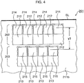
- Fig. 4 is a plan view illustrating a schematic configuration in which a part of a surface of a semiconductor chip of a comparative example 2 is enlarged to be illustrated.
- a first row 202 in which plural first I/O cells 212 are arranged in parallel at an outer periphery of an input/output circuit region 211b (at a position near the scribe line SL) and a second row 203 in which plural second I/O cells 213 are arranged in parallel at inside of the first row 202 (at a position near an internal circuit forming region 211a) are disposed at the input/output circuit region 211b.
- a first external connection terminal 214 is provided at each of the first I/O cells 212, and a second external connection terminal 215 is provided at each of the second I/O cells 213, respectively.
- the first external connection terminal 214 connected by one end of the first I/O cell 212 and positioning at upside of the first I/O cell 212 is disposed at the first row 202
- the second external connection terminal 215 connected by one end of the second I/O cell 213 and positioning at upside of the second I/O cell 213 is disposed at the second row 203, respectively.
- the separation distance is shortened in the semiconductor chip 201 of the comparative example 2 than in the semiconductor chip 101 of the comparative example 1 because "y3 ⁇ y2" as in the comparative examples 1, 2.
- the separation distance "y1" in the semiconductor chip 1 becomes "y1 ⁇ y3 ⁇ y2". In the semiconductor chip 1, it is possible to drastically shorten the separation distance compared to the comparative examples 1, 2.
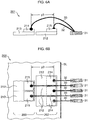
- Fig. 5A to Fig. 5E are schematic diagrams illustrating the manufacturing method of the semiconductor device in process sequence.
- lower parts of the drawings of Fig. 5A, Fig. 5B and Fig. 5C correspond to a cross section along a dotted line m-n in an upper part of the drawing in Fig. 5C .
- respective interlayer insulating films embedding respective layers are represented as "interlayer insulating films 21" as a whole.
- Fig. 5D is a side view
- Fig. 5E is a plan view.
- various kinds of semiconductor integrated circuits and so on constituting the circuit forming region 11 are formed on a semiconductor substrate 10.
- the semiconductor integrated circuit constituted by predetermined transistors, semiconductor memories, and so on is formed at the internal circuit forming region 11a, and the TTL circuit and so on are formed at the input/output circuit region 11b, respectively.
- MOS transistors 20 (only gate portions thereof are illustrated) being one of components of the TTL circuit are exemplified as illustrated in Fig. 5A .
- the wiring structure is constituted by wirings and via portions connecting the wirings and so on at upward and downward.
- plural layers of wirings connected to the semiconductor integrated circuit constituted by the predetermined transistors, semiconductor memories and so on are formed at the internal circuit forming region 11a, and plural layers of wirings connected to the TTL circuit and so on are formed at the input/output circuit region 11b, respectively.
- the wirings and the via portions at each layer of the circuit forming region 11a side and the wirings and the via portions at each layer of the input/output circuit region 11b side are formed by the same process by each layer.
- the via portion V1 connected to the semiconductor integrated circuit constituted by the predetermined transistors, the semiconductor memories and so on (connected to source/drain regions, gate electrode in case of the MOS transistor) is formed at the internal circuit forming region 11a.
- contact holes (not-illustrated) exposing a part of surfaces of the source/drain regions and so on are formed at the interlayer insulating film 21, then Ti and TiN are deposited so as to cover an internal surface of the contact hole to form a glue film (not-illustrated).
- a conductive substance, here, tungsten (W) is deposited so as to embed the contact hole via the glue film by a CVD method and so on. After that, a surface of W is smoothed by, for example, a CMP, and the via portion V3 constituted by filling the contact hole with W is formed.
- the wiring W1 to the wiring W3 and the via portions V2, V3 are appropriately formed as Cu layers as stated below by so-called a single damascene method or a dual damascene method while using, for example, Cu or an alloy thereof as a material.
- wiring grooves, openings, and so on are formed at the interlayer insulating film 21, Cu or the alloy thereof is embedded by a plating method so as to embed the wiring grooves, the openings, and so on.
- a surface thereof is smoothed by, for example, a chemical mechanical polishing (CMP), and the Cu layer filling the wiring grooves, the openings, and so on with Cu or the alloy thereof is formed.
- CMP chemical mechanical polishing
- the wiring grooves, the openings, and so on and via holes to be integrated thereto are simultaneously formed at the interlayer insulating film 21, Cu or the alloy thereof is embedded by the plating method so as to embed the wiring grooves, the openings and so on, and the via holes.
- the surface thereof is smoothed by, for example, the CMP, and the Cu layer constituted by filling the wiring grooves, the openings and so on, and the via holes with Cu or the alloy thereof is formed.
- via holes (not-illustrated) exposing a part of a surface of the wiring W3 are formed at the interlayer insulating film 21, then Ti and TiN are deposited so as to cover an internal surface of the via hole to form a glue film (not-illustrated).
- a conductive substance here, tungsten (W) is deposited so as to embed the via hole via the glue film by the CVD method and so on. After that, a surface of W is smoothed by, for example, the CMP, and the via portion V4 constituted by filling the via hole with W is formed.
- aluminum or an alloy thereof is deposited on the interlayer insulating film 21 where an upper surface of the via portion V4 exposes by a sputtering method and so on, to form an Al film (not-illustrated).
- This Al film is processed by lithography and dry etching.
- the wiring W4 constituted by connected to the via portion V4 on the interlayer insulating film 21 is thereby formed.
- a part of the wirings W1 to W4 and V2 to V4 constitutes a base structure of the first external connection terminal 14 and the second external connection terminal 15.
- the via portion V5, the first external connection terminal 14, the second external connection terminal 15, a protective film 22, and a PI film 23 are formed as illustrated in Fig. 5C .
- the via portion V5 connected to the wiring W4 being a component of the base structure of the first external connection terminal 14 and the second external connection terminal 15 is formed from among the wiring W4.
- via holes (not-illustrated) exposing a part of a surface of the wiring W4 are formed at the interlayer insulating film 21, then Ti and TiN are deposited so as to cover an internal surface of the via hole to form a glue film (not-illustrated).
- a conductive substance here, tungsten (W) is deposited so as to embed the via hole via the glue film by the CVD method and so on. After that, a surface of W is smoothed by, for example, the CMP, and the via portion V5 constituted by filling the via hole with W is formed.
- first external connection terminal 14 and the second external connection terminal 15 connected to the via portion V5 are formed.
- Al or the alloy thereof is deposited on the interlayer insulating film 21 where an upper surface of the via portion V5 exposes by the sputtering method and so on, to form an Al film (not-illustrated).
- This Al film is processed by lithography and dry etching. The process is performed to make forms of the above-stated first row 2 and second row 3. Accordingly, the first external connection terminal 14 and the second external connection terminal 15 respectively connected to the via portions 5 on the interlayer insulating film 21 are formed.
- an insulating film here, a silicon oxide film is deposited on a whole surface so as to cover the first external connection terminal 14 and the second external connection terminal 15 by the CVD method and so on.
- the silicon oxide film is processed into a predetermined form covering from surfaces to side surfaces of the first external connection terminal 14 and the second external connection terminal 15 by lithography and dray etching, to form a protective film 22.
- a cover film, here, a PI (polyimide) film 23 is formed on a whole surface, and the PI film 23 and the protective film 22 are processed by lithography and dry etching so as to expose a part of the surfaces of the first external connection terminal 14 and the second external connection terminal 15, to form openings 24.
- a cover film here, a PI (polyimide) film 23 is formed on a whole surface, and the PI film 23 and the protective film 22 are processed by lithography and dry etching so as to expose a part of the surfaces of the first external connection terminal 14 and the second external connection terminal 15, to form openings 24.
- the first row 2 constituted by the first I/O cells 12 respectively defined as occupied regions for the semiconductor integrated circuits such as the TTL circuit at the input/output circuit region 11b and the first external connection terminals 14 connected thereto, and the second row 3 constituted by the second I/O cells 13 respectively defined as occupied regions for the semiconductor integrated circuits such as the TTL circuit at the input/output circuit region 11b and the second external connection terminals 15 connected thereto are completed.
- each semiconductor chip 1 is cut out from the semiconductor substrate 10 along the scribe line.
- the first external connection terminal 14 and the second external connection terminal 15 of the semiconductor chip 1 are electrically connected to a lead frame (not-illustrated) in an assembly process as illustrated in Fig. 5D and Fig. 5E .
- the first external connection terminal 14 of the semiconductor chip 1 and a bonding finger 31 of the lead frame are connected (wire bonded) by a bonding wire 32 made of gold or the like
- the second external connection terminal 15 and the bonding finger 31 of the lead frame are connected (wire bonded) by a bonding wire 33 made of gold or the like, alternately.
- a difference between a length of the bonding wire 32 in plane view and a length of the bonding wire 33 in plane view is shortened as much as possible, to be the separation distance "y1" in the illustrated example.
- Fig. 6A is a side view
- Fig. 6B is a plane view
- the semiconductor chip 1 is molded and so on with a molding resin, and the semiconductor device is completed by going through various post-processes.
- an electrical inspection of electrical characteristic and so on of the semiconductor device is performed, for example, under a state in Fig. 5C (a state before the semiconductor chip 1 is cut out from the semiconductor substrate 10 and plural semiconductor chips 1 are formed on the semiconductor substrate 10).
- Fig. 7 is a schematic diagram illustrating a schematic configuration of an inspection device (probing device) used for the electrical inspection.
- a target of the electrical inspection is the semiconductor substrate 10 on which plural semiconductor chips 1 are formed.
- a probe card 43 used for this electrical inspection is constituted by providing plural probe holders 44 at a base thereof in rectangular. Plural probe needles 45 brought into contact with the first external connection terminal 14 and the second external connection terminal 15 of the semiconductor chip 1 are provided at the probe holder 44.
- This probing device is constituted by providing a wafer stage 41 on which the semiconductor substrate 10 is mounted to be fixed, and an inspection portion 42 provided at, for example, a lower portion of the wafer stage 41 and electrically connected to the probe needles 45 of the probe card 43 to perform the electrical inspection.
- a continuity is secured by bringing the probe needles 45 into contact with respective terminal surfaces of the plural first external connection terminals 14 and second external connection terminals 15 by inclining the probe needles 45 from a direction perpendicular to terminal surfaces, and the electrical characteristic is measured by the inspection portion 42, to perform the electrical inspection of the semiconductor chip 10.
- the present description it is possible provide a semiconductor device with high reliability capable of preventing disadvantages such as characteristic deterioration of semiconductor integrated circuits and accuracy deterioration of electrical inspection while fully securing the electrical connection from the probe needles with the first external connection terminal 14 and the second external connection terminal 15 at the electrical inspection time and enabling the higher integration and higher function of the semiconductor chip 1, by shortening the distance between the first external connection terminal 14 and the second external connection terminal 15 adjacent at the first row 2 and the second row 3 as much as possible, in the semiconductor device having the constitution in which the I/O cells where the external connection terminals are disposed are arranged in parallel in two rows.
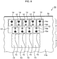
- Fig. 8 is a plan view illustrating a schematic configuration in which a part of a surface of a semiconductor chip being a component of a semiconductor device according to a modification example 1 of the set-up described with reference to figures 1 - 7 is enlarged to be illustrated.
- the first row 2 and the second row 3 are formed as same as the semiconductor chip 1 in the set-up described with reference to figures 1 - 7 .
- a bonding portion 14a to which the bonding wire is connected and an inspection target portion 14b with which the probe needles are brought into contact at the electrical inspection time of the semiconductor chip 30 are defined at different positions on each surface of the first external connection terminal 14 in addition to the constitution of the first row 2 and the second row 3 in the semiconductor chip 1.
- a bonding portion 15a to which the bonding wire is connected and an inspection target portion 15b with which the probe needles are brought into contact at the electrical inspection time of the semiconductor chip 30 are defined at different positions on each surface of the second external connection terminal 15.
- the bonding portion 14a is provided at a position near the connection portion of the first external connection terminal 14 with the first I/O cell 12, and the inspection target portion 14b is provided at a position far from the connection portion of the first external connection terminal 14 with the first I/O cell 12 on each surface of the first external connection terminal 14.
- the bonding portion 15a is provided at a position near the connection portion of the second external connection terminal 15 with the second I/O cell 13, and the inspection target portion 15b is provided at a position far from the connection portion of the second external connection terminal 15 with the second I/O cell 13 on each surface of the second external connection terminal 15.
- the bonding portion 14a is provided at outside (at a position near the scribe line SL), and the inspection target portion 14b is provided at inside (at a position far from the scribe line SL) at the first row 2.
- the bonding portion 15a is provided at inside (at a position far from the scribe line SL), and the inspection target portion 15b is provided at outside (at a position near the scribe line SL) at the second row 3.
- the semiconductor device with high reliability capable of preventing the disadvantages such as the characteristic deterioration of the semiconductor integrated circuit and the accuracy deterioration of the electrical inspection, and the disadvantage resulting from the probe needle contact for the electrical inspection, while fully securing the electrical connection of the probe needles with the first external connection terminal 14 and the second external connection terminal 15 at the electrical inspection time, and enabling higher integration, higher function of the semiconductor chip 30 by shortening the distance between the adjacent first external connection terminal 14 and second external connection terminal 15 at the first row 2 and the second row 3 as much as possible, in the semiconductor device having the constitution in which the I/O cells disposing the external connection terminals are arranged in parallel in two rows.
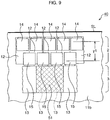
- Fig. 9 is a plan view illustrating a schematic configuration in which a part of a surface of a semiconductor chip being a component of a semiconductor device according to a modification example 2 of the set-up described with reference to figures 1 - 7 is enlarged to be illustrated.
- the first row 2 and the second row 3 are formed as same as the semiconductor chip 1 in the set-up described with reference to figures 1 - 7 .
- a function macro 51 is embedded at the region of the second I/O cell 13 at the second row 3 (at the regions of the two adjacent second I/O cells 13 in the illustrated example) in addition to the constitution of the first row 2 and the second row 3 in the semiconductor chip 1.
- the function macro 51 is constituted by integrating circuits and elements of which element characteristics are easy to be affected by an applied pressure at the connection time of the bonding wire and at the contact time of the probe needles at the electrical inspection time, for example, an A/D converter, a D/A converter, a PLL circuit, and so on.
- FIG. 10 an appearance in which a function macro 221 is provided at the semiconductor chip 201 of the comparative example 2 is illustrated in Fig. 10 .
- the second external connection terminal 215 is provided on the second I/O cell 213 at the second row 203 of the semiconductor chip 201. Accordingly, the function macro 221 including the circuits and elements of which element characteristics are easy to be affected by the applied pressure at the connection time of the bonding wire and at the contact time of the probe needles at the electrical inspection time cannot be provided on the second I/O cell 213. It is therefore necessary to provide the function macro 221 at a position, for example, apart from the second I/O cell 213 as illustrated in the drawing, and an exclusive region for the function macro 221 is required at the surface of the semiconductor chip 201.
- the function macro 51 it is possible to provide the function macro 51 so as to commonly use the occupied region with the second I/O cell 13. Accordingly, an exclusive region for the function macro 51 is not necessary, flexibility in layout improves, and requirement for higher integration, higher function of the semiconductor integrated circuit can be corresponded.
- the semiconductor device with high reliability capable of securing flexibility of layout and preventing the disadvantages such as the characteristic deterioration of the semiconductor integrated circuit and the accuracy deterioration of the electrical inspection while fully securing the electrical connection of the probe needles with the first external connection terminal 14 and the second external connection terminal 15 at the electrical inspection time and enabling the higher integration, higher function of the semiconductor chip 40 by shortening the distance between the adjacent first external connection terminal 14 and the second external connection terminal 15 at the first row 2 and the second row 3 as much as possible, in the semiconductor device having the constitution in which the I/O cells disposing the external connection terminals are arranged in parallel in two rows.
- Fig. 11 is a plan view illustrating a schematic configuration in which a part of a surface of a semiconductor chip being a component of a semiconductor device according to a modification example 3 of the set-up described with reference to figures 1 - 7 is enlarged to be illustrated.
- the first row 2 and the second row 3 are formed as same as the semiconductor chip 1 in the set-up described with reference to figures 1 - 7 .
- At least one of a power line 52 and a ground line 53 (both in the illustrated example) constituting an I/O ring is disposed at upside of the region of the second I/O cells 13 at the second row 3 in addition to the constitution of the first row 2 and the second row 3 in the semiconductor chip 1.
- the power line 52 is to supply power (V DD ) and the ground line 53 is to give a ground potential (V SS ) to various semiconductor integrated circuits and so on constituting the circuit forming region 11.
- a power line and a ground line are considered to be provided at a position, for example, inside of the second I/O cells and apart from the second I/O cells in case of the semiconductor chip in which the first row 2 and the second row 3 are disposed.
- the power line 52 and the ground line 53 are provided by using the regions of the adjacent second I/O cells 13 within the second row 3 so as to commonly use the occupied region with the second I/O cell 13. Accordingly, an exclusive region for the power line 52 and the ground line 53 is not necessary, flexibility in layout improves, and requirement for higher integration, higher function of the semiconductor integrated circuit can be corresponded.
- the semiconductor device with high reliability capable of securing flexibility in layout and preventing the disadvantages such as the characteristic deterioration of the semiconductor integrated circuit and the accuracy deterioration of the electrical inspection while fully securing the electrical connection of the probe needles with the first external connection terminal 14 and the second external connection terminal 15 at the electrical inspection time and enabling the higher integration, higher function of the semiconductor chip 50 by shortening the distance between the adjacent first external connection terminal 14 and the second external connection terminal 15 at the first row 2 and the second row 3 as much as possible, in the semiconductor device having the constitution in which the I/O cells disposing the external connection terminals are arranged in parallel in two rows.
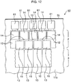
- Fig. 12 is a plan view illustrating a schematic configuration in which a part of a surface of a semiconductor chip being a component of a semiconductor device according to a modification example 4 of the set-up described with reference to figures 1 - 7 is enlarged to be illustrated.
- the first row 2 and the second row 3 are formed as same as the semiconductor chip 1 in the set-up described with reference to figures 1 - 7 .
- pads for test 61 dedicated for the electrical test are formed by being connected to the first external connection terminals 14 so as to protrude toward outside of the first row 2 (a position near the scribe line SL than the first row 2) in addition to the constitution of the first row 2 and the second row 3 in the semiconductor chip 1.
- the first external connection terminal 14 and the second external connection terminal 15 are exclusively used as the bonding pads to which the bonding wires are connected.
- the pad for test 61 is used for the electrical test, and the probe needles are brought into contact with the pad for test 61. Accordingly, in the semiconductor chip 60, the electrical test is not performed for the second row 3.
- the bonding portion and the inspection target portion are discriminated, and one is set as the first external connection terminal 14 and the other is set as the pad for test 61.
- the negative effect resulting from the contact of the probe needles at the electrical inspection time is avoided, and fully securing of the current density and the improvement of the adhesive strength between the first external connection terminal 14, the second external connection terminal 15 and the bonding wires are enabled.
- the semiconductor device with high reliability capable of preventing the disadvantages such as the characteristic deterioration of the semiconductor integrated circuit and the accuracy deterioration of the electrical inspection and the disadvantage resulting from the contact of the probe needles of the electrical inspection while fully securing the electrical connection of the probe needles with the first external connection terminal 14 and the second external connection terminal 15 at the electrical inspection time and enabling the higher integration, higher function of the semiconductor chip 60 by shortening the distance between the adjacent first external connection terminal 14 and the second external connection terminal 15 at the first row 2 and the second row 3 as much as possible, in the semiconductor device having the constitution in which the I/O cells disposing the external connection terminals are arranged in parallel in two rows.
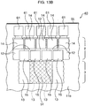
- various combinations are possible such as a constitution in which the power line 52 and the ground line 53 are disposed at upside of the region of the second I/O cells 13 including upside of the function macro 51 in the semiconductor chip 40 by combining the modification example 2 and the modification example 3 as in Fig. 13A , a constitution in which the function macro 51 is embedded at the regions of the second I/O cells 13 of the second row 3 and the dedicated pads for test 61 are disposed in the semiconductor chip 40 by combining the modification example 2 and the modification example 4 as in Fig. 13B .
- semiconductor device in the present embodiment is manufactured by the same manufacturing method with the same constitution as the semiconductor device according to the set-up described with reference to figures 1 but it is different from the set-up described with reference to figures 1 - 7 in a point that an arrangement of the first row and the second row is different.
- Fig. 14 is a plan view illustrating a schematic configuration in which a part of a surface of a semiconductor chip being a component of the semiconductor device according to this embodiment is enlarged to be illustrated.
- a first row 71 in which the plural first I/O cells 12 and first external connection terminals 14 are arranged in parallel at the outer periphery of the input/output circuit region 11b (at a position near the scribe line SL) and a second row 72 in which the plural second I/O cells 13 and second external connection terminals 15 are arranged in parallel at inside of the first row 71 (at a position near the internal circuit forming region 11a) are disposed at the input/output circuit region 11b as same as the semiconductor chip 1 in the first embodiment.
- the first external connection terminal 14 is disposed such that at least a part thereof (all in the illustrated example) positions at upside of the first I/O cell 12, and the second external connection terminal 15 is disposed such that at least a part thereof (a portion except a lower end portion in the illustrated example) positions at upside of the first I/O cell 12.
- the first external connection terminal 14 and the second external connection terminal 15 are formed at upside of the corresponding first I/O cell 12 while being arranged in parallel to face with each other.
- the first external connection terminal 14 and the second external connection terminal 15 are separated for a predetermined distance so as not to have an overlapped portion with each other, and formed in an identical layer.
- first external connection terminal 14 and the second external connection terminal 15 are disposed in proximity as much as possible at the first row 71 and the second row 72.
- the separation distance between both, here, the separation distance from a planned connection portion of the bonding wire of the first external connection terminal 14 to a planned connection portion of the bonding wire of the second external connection terminal 15 becomes "y1" as illustrated in the drawing, as same as the semiconductor chip 1 in the set-up described with reference to figures 1 - 7 .
- the semiconductor device with high reliability capable of preventing the disadvantages such as the characteristic deterioration of the semiconductor integrated circuit and the accuracy deterioration of the electrical inspection while fully securing the electrical connection of the probe needles with the first external connection terminal 14 and the second external connection terminal 15 at the electrical inspection time and enabling the higher integration, higher function of the semiconductor chip 70 by shortening the distance between the adjacent first external connection terminal 14 and the second external connection terminal 15 at the first row 71 and the second row 72 as much as possible, in the semiconductor device having the constitution in which the I/O cells disposing the external connection terminals are arranged in parallel in two rows.
- the present invention it is possible to provide a semiconductor device with high reliability capable of preventing disadvantages such as characteristic deterioration of a semiconductor integrated circuit and accuracy deterioration of an electrical inspection while fully securing an electrical connection of probe needles with external connection terminals at the electrical inspection time, and enabling higher integration, higher function of the semiconductor device by shortening a distance between adjacent external connection terminals at a first row and a second row as much as possible, in the semiconductor device having a constitution in which I/O cells disposing the external connection terminals are arranged in parallel in two rows.
Landscapes
- Semiconductor Integrated Circuits (AREA)
- Testing Or Measuring Of Semiconductors Or The Like (AREA)
- Internal Circuitry In Semiconductor Integrated Circuit Devices (AREA)
- Wire Bonding (AREA)
- Design And Manufacture Of Integrated Circuits (AREA)
Claims (13)
- Halbleitervorrichtung, umfassend:ein Halbleitersubstrat (10);eine erste Reihe (2), in der mehrere erste I/O-Zellen (12) parallel entlang einem Außenumfang des Halbleitersubstrats (10) angeordnet sind und an der Oberseite des Halbleitersubstrats (10) angeordnet sind, wobei mehrere erste Außenverbindungsanschlüsse (14) parallel entlang dem Außenumfang des Halbleitersubstrats (10) und an der Oberseite der mehreren ersten I/O-Zellen (12) angeordnet sind; undeine zweite Reihe (3), in der mehrere zweite I/O-Zellen (13) parallel an der Innenseite der ersten Reihe (2) entlang dem Außenumfang des Halbleitersubstrats (10) angeordnet sind und an der Oberseite des Halbleitersubstrats (10) angeordnet sind, wobei mehrere zweite Außenverbindungsanschlüsse (15) parallel entlang dem Außenumfang des Halbleitersubstrats (10) angeordnet sind,wobei die mehreren ersten I/O-Zellen (12) an einem Außenumfang des Halbleitersubstrats (10) angeordnet sind und die mehreren zweiten I/O-Zellen (13) parallel innerhalb der ersten Reihe angeordnet sind und die mehreren ersten I/O-Zellen (12) getrennt von den mehreren zweiten I/O-Zellen (13) angeordnet sind, undwobei jeder der zweiten Außenverbindungsanschlüsse (15) derart angeordnet ist, dass ein erster Teil davon an der Oberseite einer entsprechenden der mehreren zweiten I/O-Zellen (13) angeordnet ist und ein zweiter Teil davon an der Oberseite einer entsprechenden der ersten I/O-Zellen (12) angeordnet ist.
- Halbleitervorrichtung nach Anspruch 1,
wobei die ersten Außenverbindungsanschlüsse (14) und die zweiten Außenverbindungsanschlüsse (15) in der ebenengleichen Schicht ausgebildet sind. - Halbleitervorrichtung nach Anspruch 2,
wobei die zweiten Außenverbindungsanschlüsse (15) oberhalb einer Grenze von zwei benachbarten ersten I/O-Zellen (12) ausgebildet sind. - Halbleitervorrichtung nach Anspruch 3,
wobei jeder der ersten Außenverbindungsanschlüsse (14) und jeder der zweiten Außenverbindungsanschlüsse (15) derart ausgebildet sind, dass sie parallel einander gegenüberliegend angeordnet sind. - Halbleitervorrichtung nach Anspruch 4,
wobei jeder der ersten Außenverbindungsanschlüsse (14) und jeder der zweiten Außenverbindungsanschlüsse (15) einen Bonding-Abschnitt zur Außenverbindung und einen Prüfzielabschnitt, der derart ausgebildet ist, dass während der elektrischen Prüfung der Halbleitervorrichtung eine Sondennadel mit dem Prüfzielabschnitt an verschiedenen Positionen in Kontakt gebracht werden kann, aufweist, wobei der Bonding-Abschnitt zum Verbinden eines Bonding-Drahts dient,
wobei der Bonding-Abschnitt an der ersten Reihe (2) näher bei dem Außenumfang des Halbleitersubstrats (10) als der Prüfzielabschnitt an der ersten Reihe (2) angeordnet ist, und wobei der Bonding-Abschnitt an der zweiten Reihe (3) weiter von dem Außenumfang des Halbleitersubstrats (10) entfernt als der Prüfzielabschnitt an der zweiten Reihe (3) angeordnet ist. - Halbleitervorrichtung nach Anspruch 5,
ferner umfassend einen Funktionsmakro (51), der ausgebildet ist, um eine belegte Region in der Halbleitervorrichtung mit einer der zweiten I/O-Zellen (13) gemeinsam zu nutzen. - Verfahren zur Herstellung einer Halbleitervorrichtung, umfassend:Ausbilden einer ersten Reihe (2), die durch mehrere erste I/O-Zellen (12) gebildet wird, welche parallel entlang einem Außenumfang des Halbleitersubstrats (10) angeordnet werden und an der Oberseite des Halbleitersubstrats (10) angeordnet werden, wobei mehrere erste Außenverbindungsanschlüsse (14) parallel entlang dem Außenumfang des Halbleitersubstrats (10) und an der Oberseite der mehreren ersten I/O-Zellen (12) angeordnet werden, und Ausbilden einer zweiten Reihe (3), die durch mehrere zweite I/O-Zellen (13) gebildet wird,welche parallel an der Innenseite der ersten Reihe (2) entlang dem Außenumfang des Halbleitersubstrats (10) angeordnet werden und an der Oberseite eines Halbleitersubstrats (10) angeordnet werden, wobei mehrere zweite Außenverbindungsanschlüsse (15) parallel entlang dem Außenumfang des Halbleitersubstrats (10) angeordnet werden,wobei die mehreren ersten I/O-Zellen (12) an einem Außenumfang des Halbleitersubstrats (10) angeordnet werden und die mehreren zweiten I/O-Zellen (13) parallel innerhalb der ersten Reihe angeordnet werden und die mehreren ersten I/O-Zellen (12) getrennt von den mehreren zweiten I/O-Zellen (13) angeordnet werden, undwobei jeder der zweiten Außenverbindungsanschlüsse (15) derart angeordnet wird, dass mindestens ein erster Teil davon an der Oberseite einer entsprechenden der mehreren zweiten I/O-Zellen (13) angeordnet wird und ein zweiter Teil davon an der Oberseite einer entsprechenden der ersten I/O-Zellen (12) angeordnet wird.
- Verfahren zur Herstellung der Halbleitervorrichtung nach Anspruch 7,
wobei die ersten Außenverbindungsanschlüsse (14) und die zweiten Außenverbindungsanschlüsse (15) in der ebenengleichen Schicht ausgebildet werden. - Verfahren zur Herstellung der Halbleitervorrichtung nach Anspruch 8,
wobei die zweiten Außenverbindungsanschlüsse oberhalb einer Grenze von zwei benachbarten ersten I/O-Zellen (12) ausgebildet werden. - Verfahren zur Herstellung der Halbleitervorrichtung nach Anspruch 9,
wobei jeder der ersten Außenverbindungsanschlüsse (14) und jeder der zweiten Außenverbindungsanschlüsse (15) parallel einander gegenüberliegend ausgebildet werden. - Verfahren zur Herstellung der Halbleitervorrichtung nach Anspruch 10, ferner umfassend:
elektrisches Verbinden der ersten Außenverbindungsanschlüsse (14) und der zweiten Außenverbindungsanschlüsse (15) mit externen Anschlüssen abwechselnd von außerhalb des Halbleitersubstrats (10) nach dem Ausbilden der ersten Reihe (2) und der zweiten Reihe (3). - Verfahren zur Herstellung der Halbleitervorrichtung nach Anspruch 11,
wobei jeder der ersten Außenverbindungsanschlüsse (14) und jeder der zweiten Außenverbindungsanschlüsse (15) einen Bonding-Abschnitt zur Außenverbindung und einen Prüfzielabschnitt, der derart ausgebildet wird, dass während der elektrischen Prüfung der Halbleitervorrichtung eine Sondennadel mit dem Prüfzielabschnitt an verschiedenen Positionen in Kontakt gebracht werden kann, aufweist, wobei der Bonding-Abschnitt zum Verbinden eines Bonding-Drahts dient,
wobei der Bonding-Abschnitt an der ersten Reihe (2) näher bei dem Außenumfang des Halbleitersubstrats (10) als der Prüfzielabschnitt an der ersten Reihe (2) angeordnet wird, und wobei der Bonding-Abschnitt an der zweiten Reihe (3) weiter von dem Außenumfang des Halbleitersubstrats (10) entfernt als der Prüfzielabschnitt an der zweiten Reihe (3) angeordnet wird. - Verfahren zur Herstellung der Halbleitervorrichtung nach Anspruch 12,
ferner umfassend einen Funktionsmakro (51), der eine belegte Region in der Halbleitervorrichtung mit einer der zweiten I/O-Zellen (13) gemeinsam nutzt.
Applications Claiming Priority (1)
| Application Number | Priority Date | Filing Date | Title |
|---|---|---|---|
| PCT/JP2007/075249 WO2009084100A1 (ja) | 2007-12-28 | 2007-12-28 | 半導体装置及びその製造方法 |
Publications (3)
| Publication Number | Publication Date |
|---|---|
| EP2242095A1 EP2242095A1 (de) | 2010-10-20 |
| EP2242095A4 EP2242095A4 (de) | 2013-06-05 |
| EP2242095B1 true EP2242095B1 (de) | 2021-05-19 |
Family
ID=40823840
Family Applications (1)
| Application Number | Title | Priority Date | Filing Date |
|---|---|---|---|
| EP07860452.7A Active EP2242095B1 (de) | 2007-12-28 | 2007-12-28 | Halbleiterbauelement und verfahren zu seiner herstellung |
Country Status (7)
| Country | Link |
|---|---|
| US (1) | US8519551B2 (de) |
| EP (1) | EP2242095B1 (de) |
| JP (1) | JP5012908B2 (de) |
| KR (1) | KR101224426B1 (de) |
| CN (1) | CN101911284B (de) |
| TW (1) | TW200929401A (de) |
| WO (1) | WO2009084100A1 (de) |
Families Citing this family (13)
| Publication number | Priority date | Publication date | Assignee | Title |
|---|---|---|---|---|
| US8242613B2 (en) * | 2010-09-01 | 2012-08-14 | Freescale Semiconductor, Inc. | Bond pad for semiconductor die |
| JP6118652B2 (ja) * | 2013-02-22 | 2017-04-19 | ルネサスエレクトロニクス株式会社 | 半導体チップ及び半導体装置 |
| JP2015079848A (ja) * | 2013-10-17 | 2015-04-23 | シナプティクス・ディスプレイ・デバイス株式会社 | 表示装置駆動用半導体集積回路装置 |
| JP2015088576A (ja) * | 2013-10-30 | 2015-05-07 | ルネサスエレクトロニクス株式会社 | 半導体装置および半導体装置の製造方法 |
| KR20160090705A (ko) * | 2015-01-22 | 2016-08-01 | 에스케이하이닉스 주식회사 | 패키지 기판 및 이를 이용한 반도체 패키지 |
| JP6664897B2 (ja) * | 2015-07-22 | 2020-03-13 | ルネサスエレクトロニクス株式会社 | 半導体装置 |
| JP6767789B2 (ja) * | 2016-06-29 | 2020-10-14 | ローム株式会社 | 半導体装置 |
| US9899324B1 (en) * | 2016-11-28 | 2018-02-20 | Globalfoundries Inc. | Structure and method of conductive bus bar for resistive seed substrate plating |
| US10867894B2 (en) * | 2018-10-11 | 2020-12-15 | Asahi Kasei Microdevices Corporation | Semiconductor element including encapsulated lead frames |
| CN112868094B (zh) | 2018-10-19 | 2024-05-28 | 株式会社索思未来 | 半导体芯片 |
| JP7721275B2 (ja) * | 2021-01-22 | 2025-08-12 | キヤノン株式会社 | 半導体素子、機器、チップ |
| CN113791335B (zh) * | 2021-10-09 | 2022-09-02 | 南通芯盟测试研究院运营管理有限公司 | 不同排列组合的探针卡 |
| JP7631264B2 (ja) * | 2022-08-09 | 2025-02-18 | キヤノン株式会社 | 液体吐出ユニット及びその製造方法 |
Family Cites Families (20)
| Publication number | Priority date | Publication date | Assignee | Title |
|---|---|---|---|---|
| JP3504421B2 (ja) * | 1996-03-12 | 2004-03-08 | 株式会社ルネサステクノロジ | 半導体装置 |
| JP2910724B2 (ja) * | 1997-04-09 | 1999-06-23 | 日本電気株式会社 | 入出力バッファ |
| JPH11307601A (ja) | 1998-04-16 | 1999-11-05 | Mitsubishi Electric Corp | 半導体装置 |
| US6242814B1 (en) * | 1998-07-31 | 2001-06-05 | Lsi Logic Corporation | Universal I/O pad structure for in-line or staggered wire bonding or arrayed flip-chip assembly |
| TW442945B (en) | 1998-11-20 | 2001-06-23 | Sony Computer Entertainment Inc | Integrated circuit chip, integrated circuit device, printed circuit board and electronic machine |
| JP3407025B2 (ja) | 2000-06-08 | 2003-05-19 | Necエレクトロニクス株式会社 | 半導体装置及びその製造方法 |
| JP2002299567A (ja) * | 2001-04-02 | 2002-10-11 | Sony Corp | 半導体素子 |
| TW495940B (en) * | 2001-07-20 | 2002-07-21 | Via Tech Inc | Method for forming a grid array packaged integrated circuit |
| JP4025044B2 (ja) * | 2001-09-27 | 2007-12-19 | 株式会社東芝 | 半導体集積回路装置 |
| US6858945B2 (en) * | 2002-08-21 | 2005-02-22 | Broadcom Corporation | Multi-concentric pad arrangements for integrated circuit pads |
| US6856022B2 (en) * | 2003-03-31 | 2005-02-15 | Matsushita Electric Industrial Co., Ltd. | Semiconductor device |
| JPWO2004093191A1 (ja) * | 2003-04-11 | 2006-07-06 | 富士通株式会社 | 半導体装置 |
| US6953997B1 (en) * | 2004-06-04 | 2005-10-11 | Taiwan Semiconductor Manufacturing Company, Ltd. | Semiconductor device with improved bonding pad connection and placement |
| US7071561B2 (en) * | 2004-06-08 | 2006-07-04 | Taiwan Semiconductor Manufacturing Company, Ltd. | Semiconductor device and method of manufacture thereof with two or more bond pad connections for each input/output cell |
| JP4370215B2 (ja) | 2004-07-29 | 2009-11-25 | オリンパス株式会社 | 投影表示装置 |
| US20070111376A1 (en) * | 2005-04-29 | 2007-05-17 | Stats Chippac Ltd. | Integrated circuit package system |
| JP4708865B2 (ja) * | 2005-06-01 | 2011-06-22 | 川崎マイクロエレクトロニクス株式会社 | 半導体装置 |
| US7829983B2 (en) | 2005-08-01 | 2010-11-09 | Panasonic Corporation | Semiconductor device |
| JP2007305822A (ja) * | 2006-05-12 | 2007-11-22 | Kawasaki Microelectronics Kk | 半導体集積回路 |
| WO2007136932A2 (en) * | 2006-05-16 | 2007-11-29 | Freescale Semiconductor Inc. | Integrated circuit having pads and input/output (i/o) cells |
-
2007
- 2007-12-28 TW TW096150765A patent/TW200929401A/zh unknown
- 2007-12-28 EP EP07860452.7A patent/EP2242095B1/de active Active
- 2007-12-28 WO PCT/JP2007/075249 patent/WO2009084100A1/ja not_active Ceased
- 2007-12-28 KR KR1020107013227A patent/KR101224426B1/ko not_active Expired - Fee Related
- 2007-12-28 CN CN2007801020640A patent/CN101911284B/zh active Active
- 2007-12-28 JP JP2009547844A patent/JP5012908B2/ja active Active
-
2010
- 2010-06-18 US US12/818,588 patent/US8519551B2/en active Active
Non-Patent Citations (1)
| Title |
|---|
| None * |
Also Published As
| Publication number | Publication date |
|---|---|
| JP5012908B2 (ja) | 2012-08-29 |
| KR101224426B1 (ko) | 2013-01-22 |
| EP2242095A4 (de) | 2013-06-05 |
| US20100252830A1 (en) | 2010-10-07 |
| KR20100087222A (ko) | 2010-08-03 |
| EP2242095A1 (de) | 2010-10-20 |
| WO2009084100A1 (ja) | 2009-07-09 |
| TW200929401A (en) | 2009-07-01 |
| CN101911284A (zh) | 2010-12-08 |
| JPWO2009084100A1 (ja) | 2011-05-12 |
| CN101911284B (zh) | 2013-08-21 |
| US8519551B2 (en) | 2013-08-27 |
Similar Documents
| Publication | Publication Date | Title |
|---|---|---|
| US8519551B2 (en) | Semiconductor device with I/O cell and external connection terminal and method of manufacturing the same | |
| TWI730028B (zh) | 半導體裝置及其製造方法 | |
| CN100514076C (zh) | 具有测试焊盘结构的集成电路以及测试方法 | |
| JP5342154B2 (ja) | 半導体装置の製造方法 | |
| US8304857B2 (en) | Semiconductor device | |
| CN114203657B (zh) | 半导体装置 | |
| US20200303268A1 (en) | Semiconductor device including residual test pattern | |
| US8482002B2 (en) | Semiconductor device including bonding pads and semiconductor package including the semiconductor device | |
| JP5467736B2 (ja) | 半導体集積回路 | |
| JP4611067B2 (ja) | 半導体装置 | |
| JP2014143236A (ja) | 半導体装置 | |
| US7501710B2 (en) | Semiconductor integrated circuit and method of manufacturing the same | |
| TW202327012A (zh) | 半導體記憶裝置及其製造方法 | |
| CN100421241C (zh) | 半导体集成电路 | |
| JP2004296464A (ja) | 半導体装置 | |
| CN114429917A (zh) | 半导体装置 | |
| CN116884955A (zh) | 半导体结构及测试方法 | |
| HK1251818A1 (zh) | 半导体器件及其制造方法 | |
| JP2003297922A (ja) | 半導体装置及び半導体装置の製造方法 |
Legal Events
| Date | Code | Title | Description |
|---|---|---|---|
| PUAI | Public reference made under article 153(3) epc to a published international application that has entered the european phase |
Free format text: ORIGINAL CODE: 0009012 |
|
| 17P | Request for examination filed |
Effective date: 20100721 |
|
| AK | Designated contracting states |
Kind code of ref document: A1 Designated state(s): AT BE BG CH CY CZ DE DK EE ES FI FR GB GR HU IE IS IT LI LT LU LV MC MT NL PL PT RO SE SI SK TR |
|
| AX | Request for extension of the european patent |
Extension state: AL BA HR MK RS |
|
| DAX | Request for extension of the european patent (deleted) | ||
| A4 | Supplementary search report drawn up and despatched |
Effective date: 20130507 |
|
| RIC1 | Information provided on ipc code assigned before grant |
Ipc: H01L 23/485 20060101AFI20130430BHEP Ipc: H01L 21/66 20060101ALI20130430BHEP Ipc: H01L 23/528 20060101ALI20130430BHEP Ipc: H01L 21/822 20060101ALI20130430BHEP Ipc: H01L 27/04 20060101ALI20130430BHEP Ipc: G06F 17/50 20060101ALI20130430BHEP |
|
| RAP1 | Party data changed (applicant data changed or rights of an application transferred) |
Owner name: SOCIONEXT INC. |
|
| STAA | Information on the status of an ep patent application or granted ep patent |
Free format text: STATUS: EXAMINATION IS IN PROGRESS |
|
| 17Q | First examination report despatched |
Effective date: 20170822 |
|
| REG | Reference to a national code |
Ref country code: DE Ref legal event code: R079 Ref document number: 602007061134 Country of ref document: DE Free format text: PREVIOUS MAIN CLASS: H01L0021822000 Ipc: H01L0023000000 |
|
| RIC1 | Information provided on ipc code assigned before grant |
Ipc: H01L 23/528 20060101ALI20200721BHEP Ipc: H01L 21/66 20060101ALI20200721BHEP Ipc: H01L 23/00 20060101AFI20200721BHEP Ipc: H01L 27/02 20060101ALI20200721BHEP |
|
| GRAP | Despatch of communication of intention to grant a patent |
Free format text: ORIGINAL CODE: EPIDOSNIGR1 |
|
| STAA | Information on the status of an ep patent application or granted ep patent |
Free format text: STATUS: GRANT OF PATENT IS INTENDED |
|
| INTG | Intention to grant announced |
Effective date: 20200915 |
|
| RIN1 | Information on inventor provided before grant (corrected) |
Inventor name: OSAJIMA, TORU |
|
| GRAJ | Information related to disapproval of communication of intention to grant by the applicant or resumption of examination proceedings by the epo deleted |
Free format text: ORIGINAL CODE: EPIDOSDIGR1 |
|
| STAA | Information on the status of an ep patent application or granted ep patent |
Free format text: STATUS: EXAMINATION IS IN PROGRESS |
|
| GRAP | Despatch of communication of intention to grant a patent |
Free format text: ORIGINAL CODE: EPIDOSNIGR1 |
|
| STAA | Information on the status of an ep patent application or granted ep patent |
Free format text: STATUS: GRANT OF PATENT IS INTENDED |
|
| INTC | Intention to grant announced (deleted) | ||
| INTG | Intention to grant announced |
Effective date: 20210222 |
|
| GRAS | Grant fee paid |
Free format text: ORIGINAL CODE: EPIDOSNIGR3 |
|
| GRAA | (expected) grant |
Free format text: ORIGINAL CODE: 0009210 |
|
| STAA | Information on the status of an ep patent application or granted ep patent |
Free format text: STATUS: THE PATENT HAS BEEN GRANTED |
|
| AK | Designated contracting states |
Kind code of ref document: B1 Designated state(s): AT BE BG CH CY CZ DE DK EE ES FI FR GB GR HU IE IS IT LI LT LU LV MC MT NL PL PT RO SE SI SK TR |
|
| REG | Reference to a national code |
Ref country code: GB Ref legal event code: FG4D |
|
| REG | Reference to a national code |
Ref country code: CH Ref legal event code: EP |
|
| REG | Reference to a national code |
Ref country code: DE Ref legal event code: R096 Ref document number: 602007061134 Country of ref document: DE |
|
| REG | Reference to a national code |
Ref country code: AT Ref legal event code: REF Ref document number: 1394822 Country of ref document: AT Kind code of ref document: T Effective date: 20210615 |
|
| REG | Reference to a national code |
Ref country code: IE Ref legal event code: FG4D |
|
| REG | Reference to a national code |
Ref country code: LT Ref legal event code: MG9D |
|
| REG | Reference to a national code |
Ref country code: AT Ref legal event code: MK05 Ref document number: 1394822 Country of ref document: AT Kind code of ref document: T Effective date: 20210519 |
|
| REG | Reference to a national code |
Ref country code: NL Ref legal event code: MP Effective date: 20210519 |
|
| PG25 | Lapsed in a contracting state [announced via postgrant information from national office to epo] |
Ref country code: LT Free format text: LAPSE BECAUSE OF FAILURE TO SUBMIT A TRANSLATION OF THE DESCRIPTION OR TO PAY THE FEE WITHIN THE PRESCRIBED TIME-LIMIT Effective date: 20210519 Ref country code: FI Free format text: LAPSE BECAUSE OF FAILURE TO SUBMIT A TRANSLATION OF THE DESCRIPTION OR TO PAY THE FEE WITHIN THE PRESCRIBED TIME-LIMIT Effective date: 20210519 Ref country code: AT Free format text: LAPSE BECAUSE OF FAILURE TO SUBMIT A TRANSLATION OF THE DESCRIPTION OR TO PAY THE FEE WITHIN THE PRESCRIBED TIME-LIMIT Effective date: 20210519 Ref country code: BG Free format text: LAPSE BECAUSE OF FAILURE TO SUBMIT A TRANSLATION OF THE DESCRIPTION OR TO PAY THE FEE WITHIN THE PRESCRIBED TIME-LIMIT Effective date: 20210819 |
|
| PG25 | Lapsed in a contracting state [announced via postgrant information from national office to epo] |
Ref country code: LV Free format text: LAPSE BECAUSE OF FAILURE TO SUBMIT A TRANSLATION OF THE DESCRIPTION OR TO PAY THE FEE WITHIN THE PRESCRIBED TIME-LIMIT Effective date: 20210519 Ref country code: GR Free format text: LAPSE BECAUSE OF FAILURE TO SUBMIT A TRANSLATION OF THE DESCRIPTION OR TO PAY THE FEE WITHIN THE PRESCRIBED TIME-LIMIT Effective date: 20210820 Ref country code: IS Free format text: LAPSE BECAUSE OF FAILURE TO SUBMIT A TRANSLATION OF THE DESCRIPTION OR TO PAY THE FEE WITHIN THE PRESCRIBED TIME-LIMIT Effective date: 20210919 Ref country code: SE Free format text: LAPSE BECAUSE OF FAILURE TO SUBMIT A TRANSLATION OF THE DESCRIPTION OR TO PAY THE FEE WITHIN THE PRESCRIBED TIME-LIMIT Effective date: 20210519 Ref country code: PT Free format text: LAPSE BECAUSE OF FAILURE TO SUBMIT A TRANSLATION OF THE DESCRIPTION OR TO PAY THE FEE WITHIN THE PRESCRIBED TIME-LIMIT Effective date: 20210920 Ref country code: PL Free format text: LAPSE BECAUSE OF FAILURE TO SUBMIT A TRANSLATION OF THE DESCRIPTION OR TO PAY THE FEE WITHIN THE PRESCRIBED TIME-LIMIT Effective date: 20210519 Ref country code: ES Free format text: LAPSE BECAUSE OF FAILURE TO SUBMIT A TRANSLATION OF THE DESCRIPTION OR TO PAY THE FEE WITHIN THE PRESCRIBED TIME-LIMIT Effective date: 20210519 |
|
| PG25 | Lapsed in a contracting state [announced via postgrant information from national office to epo] |
Ref country code: NL Free format text: LAPSE BECAUSE OF FAILURE TO SUBMIT A TRANSLATION OF THE DESCRIPTION OR TO PAY THE FEE WITHIN THE PRESCRIBED TIME-LIMIT Effective date: 20210519 |
|
| PG25 | Lapsed in a contracting state [announced via postgrant information from national office to epo] |
Ref country code: DK Free format text: LAPSE BECAUSE OF FAILURE TO SUBMIT A TRANSLATION OF THE DESCRIPTION OR TO PAY THE FEE WITHIN THE PRESCRIBED TIME-LIMIT Effective date: 20210519 Ref country code: EE Free format text: LAPSE BECAUSE OF FAILURE TO SUBMIT A TRANSLATION OF THE DESCRIPTION OR TO PAY THE FEE WITHIN THE PRESCRIBED TIME-LIMIT Effective date: 20210519 Ref country code: CZ Free format text: LAPSE BECAUSE OF FAILURE TO SUBMIT A TRANSLATION OF THE DESCRIPTION OR TO PAY THE FEE WITHIN THE PRESCRIBED TIME-LIMIT Effective date: 20210519 Ref country code: SK Free format text: LAPSE BECAUSE OF FAILURE TO SUBMIT A TRANSLATION OF THE DESCRIPTION OR TO PAY THE FEE WITHIN THE PRESCRIBED TIME-LIMIT Effective date: 20210519 Ref country code: RO Free format text: LAPSE BECAUSE OF FAILURE TO SUBMIT A TRANSLATION OF THE DESCRIPTION OR TO PAY THE FEE WITHIN THE PRESCRIBED TIME-LIMIT Effective date: 20210519 |
|
| REG | Reference to a national code |
Ref country code: DE Ref legal event code: R097 Ref document number: 602007061134 Country of ref document: DE |
|
| PLBE | No opposition filed within time limit |
Free format text: ORIGINAL CODE: 0009261 |
|
| STAA | Information on the status of an ep patent application or granted ep patent |
Free format text: STATUS: NO OPPOSITION FILED WITHIN TIME LIMIT |
|
| 26N | No opposition filed |
Effective date: 20220222 |
|
| PG25 | Lapsed in a contracting state [announced via postgrant information from national office to epo] |
Ref country code: IS Free format text: LAPSE BECAUSE OF FAILURE TO SUBMIT A TRANSLATION OF THE DESCRIPTION OR TO PAY THE FEE WITHIN THE PRESCRIBED TIME-LIMIT Effective date: 20210919 |
|
| PG25 | Lapsed in a contracting state [announced via postgrant information from national office to epo] |
Ref country code: MC Free format text: LAPSE BECAUSE OF FAILURE TO SUBMIT A TRANSLATION OF THE DESCRIPTION OR TO PAY THE FEE WITHIN THE PRESCRIBED TIME-LIMIT Effective date: 20210519 Ref country code: IT Free format text: LAPSE BECAUSE OF FAILURE TO SUBMIT A TRANSLATION OF THE DESCRIPTION OR TO PAY THE FEE WITHIN THE PRESCRIBED TIME-LIMIT Effective date: 20210519 |
|
| REG | Reference to a national code |
Ref country code: CH Ref legal event code: PL |
|
| GBPC | Gb: european patent ceased through non-payment of renewal fee |
Effective date: 20211228 |
|
| REG | Reference to a national code |
Ref country code: BE Ref legal event code: MM Effective date: 20211231 |
|
| PG25 | Lapsed in a contracting state [announced via postgrant information from national office to epo] |
Ref country code: LU Free format text: LAPSE BECAUSE OF NON-PAYMENT OF DUE FEES Effective date: 20211228 Ref country code: IE Free format text: LAPSE BECAUSE OF NON-PAYMENT OF DUE FEES Effective date: 20211228 Ref country code: GB Free format text: LAPSE BECAUSE OF NON-PAYMENT OF DUE FEES Effective date: 20211228 |
|
| PG25 | Lapsed in a contracting state [announced via postgrant information from national office to epo] |
Ref country code: FR Free format text: LAPSE BECAUSE OF NON-PAYMENT OF DUE FEES Effective date: 20211231 Ref country code: BE Free format text: LAPSE BECAUSE OF NON-PAYMENT OF DUE FEES Effective date: 20211231 |
|
| PG25 | Lapsed in a contracting state [announced via postgrant information from national office to epo] |
Ref country code: LI Free format text: LAPSE BECAUSE OF NON-PAYMENT OF DUE FEES Effective date: 20211231 Ref country code: CH Free format text: LAPSE BECAUSE OF NON-PAYMENT OF DUE FEES Effective date: 20211231 |
|
| PG25 | Lapsed in a contracting state [announced via postgrant information from national office to epo] |
Ref country code: HU Free format text: LAPSE BECAUSE OF FAILURE TO SUBMIT A TRANSLATION OF THE DESCRIPTION OR TO PAY THE FEE WITHIN THE PRESCRIBED TIME-LIMIT; INVALID AB INITIO Effective date: 20071228 Ref country code: CY Free format text: LAPSE BECAUSE OF FAILURE TO SUBMIT A TRANSLATION OF THE DESCRIPTION OR TO PAY THE FEE WITHIN THE PRESCRIBED TIME-LIMIT Effective date: 20210519 |
|
| PGFP | Annual fee paid to national office [announced via postgrant information from national office to epo] |
Ref country code: DE Payment date: 20231214 Year of fee payment: 17 |
|
| PG25 | Lapsed in a contracting state [announced via postgrant information from national office to epo] |
Ref country code: MT Free format text: LAPSE BECAUSE OF FAILURE TO SUBMIT A TRANSLATION OF THE DESCRIPTION OR TO PAY THE FEE WITHIN THE PRESCRIBED TIME-LIMIT Effective date: 20210519 |
|
| REG | Reference to a national code |
Ref country code: DE Ref legal event code: R119 Ref document number: 602007061134 Country of ref document: DE |
|
| PG25 | Lapsed in a contracting state [announced via postgrant information from national office to epo] |
Ref country code: DE Free format text: LAPSE BECAUSE OF NON-PAYMENT OF DUE FEES Effective date: 20250701 |
|
| PG25 | Lapsed in a contracting state [announced via postgrant information from national office to epo] |
Ref country code: TR Free format text: LAPSE BECAUSE OF FAILURE TO SUBMIT A TRANSLATION OF THE DESCRIPTION OR TO PAY THE FEE WITHIN THE PRESCRIBED TIME-LIMIT Effective date: 20210519 |