EP2248868B1 - Leuchtstoffmaterial und leuchstoffelement - Google Patents
Leuchtstoffmaterial und leuchstoffelement Download PDFInfo
- Publication number
- EP2248868B1 EP2248868B1 EP09714824.1A EP09714824A EP2248868B1 EP 2248868 B1 EP2248868 B1 EP 2248868B1 EP 09714824 A EP09714824 A EP 09714824A EP 2248868 B1 EP2248868 B1 EP 2248868B1
- Authority
- EP
- European Patent Office
- Prior art keywords
- group
- compound
- light emitting
- emitting device
- aryl
- Prior art date
- Legal status (The legal status is an assumption and is not a legal conclusion. Google has not performed a legal analysis and makes no representation as to the accuracy of the status listed.)
- Not-in-force
Links
Classifications
-
- H—ELECTRICITY
- H10—SEMICONDUCTOR DEVICES; ELECTRIC SOLID-STATE DEVICES NOT OTHERWISE PROVIDED FOR
- H10K—ORGANIC ELECTRIC SOLID-STATE DEVICES
- H10K85/00—Organic materials used in the body or electrodes of devices covered by this subclass
- H10K85/60—Organic compounds having low molecular weight
- H10K85/615—Polycyclic condensed aromatic hydrocarbons, e.g. anthracene
- H10K85/624—Polycyclic condensed aromatic hydrocarbons, e.g. anthracene containing six or more rings
-
- C—CHEMISTRY; METALLURGY
- C07—ORGANIC CHEMISTRY
- C07C—ACYCLIC OR CARBOCYCLIC COMPOUNDS
- C07C211/00—Compounds containing amino groups bound to a carbon skeleton
- C07C211/43—Compounds containing amino groups bound to a carbon skeleton having amino groups bound to carbon atoms of six-membered aromatic rings of the carbon skeleton
- C07C211/57—Compounds containing amino groups bound to a carbon skeleton having amino groups bound to carbon atoms of six-membered aromatic rings of the carbon skeleton having amino groups bound to carbon atoms of six-membered aromatic rings being part of condensed ring systems of the carbon skeleton
- C07C211/61—Compounds containing amino groups bound to a carbon skeleton having amino groups bound to carbon atoms of six-membered aromatic rings of the carbon skeleton having amino groups bound to carbon atoms of six-membered aromatic rings being part of condensed ring systems of the carbon skeleton with at least one of the condensed ring systems formed by three or more rings
-
- C—CHEMISTRY; METALLURGY
- C09—DYES; PAINTS; POLISHES; NATURAL RESINS; ADHESIVES; COMPOSITIONS NOT OTHERWISE PROVIDED FOR; APPLICATIONS OF MATERIALS NOT OTHERWISE PROVIDED FOR
- C09K—MATERIALS FOR MISCELLANEOUS APPLICATIONS, NOT PROVIDED FOR ELSEWHERE
- C09K11/00—Luminescent materials, e.g. electroluminescent or chemiluminescent
- C09K11/06—Luminescent materials, e.g. electroluminescent or chemiluminescent containing organic luminescent materials
-
- H—ELECTRICITY
- H10—SEMICONDUCTOR DEVICES; ELECTRIC SOLID-STATE DEVICES NOT OTHERWISE PROVIDED FOR
- H10K—ORGANIC ELECTRIC SOLID-STATE DEVICES
- H10K50/00—Organic light-emitting devices
- H10K50/10—OLEDs or polymer light-emitting diodes [PLED]
- H10K50/11—OLEDs or polymer light-emitting diodes [PLED] characterised by the electroluminescent [EL] layers
-
- H—ELECTRICITY
- H10—SEMICONDUCTOR DEVICES; ELECTRIC SOLID-STATE DEVICES NOT OTHERWISE PROVIDED FOR
- H10K—ORGANIC ELECTRIC SOLID-STATE DEVICES
- H10K50/00—Organic light-emitting devices
- H10K50/10—OLEDs or polymer light-emitting diodes [PLED]
- H10K50/17—Carrier injection layers
-
- H—ELECTRICITY
- H10—SEMICONDUCTOR DEVICES; ELECTRIC SOLID-STATE DEVICES NOT OTHERWISE PROVIDED FOR
- H10K—ORGANIC ELECTRIC SOLID-STATE DEVICES
- H10K85/00—Organic materials used in the body or electrodes of devices covered by this subclass
- H10K85/40—Organosilicon compounds, e.g. TIPS pentacene
-
- H—ELECTRICITY
- H10—SEMICONDUCTOR DEVICES; ELECTRIC SOLID-STATE DEVICES NOT OTHERWISE PROVIDED FOR
- H10K—ORGANIC ELECTRIC SOLID-STATE DEVICES
- H10K85/00—Organic materials used in the body or electrodes of devices covered by this subclass
- H10K85/60—Organic compounds having low molecular weight
- H10K85/631—Amine compounds having at least two aryl rest on at least one amine-nitrogen atom, e.g. triphenylamine
- H10K85/633—Amine compounds having at least two aryl rest on at least one amine-nitrogen atom, e.g. triphenylamine comprising polycyclic condensed aromatic hydrocarbons as substituents on the nitrogen atom
-
- H—ELECTRICITY
- H10—SEMICONDUCTOR DEVICES; ELECTRIC SOLID-STATE DEVICES NOT OTHERWISE PROVIDED FOR
- H10K—ORGANIC ELECTRIC SOLID-STATE DEVICES
- H10K85/00—Organic materials used in the body or electrodes of devices covered by this subclass
- H10K85/60—Organic compounds having low molecular weight
- H10K85/649—Aromatic compounds comprising a hetero atom
- H10K85/654—Aromatic compounds comprising a hetero atom comprising only nitrogen as heteroatom
-
- H—ELECTRICITY
- H10—SEMICONDUCTOR DEVICES; ELECTRIC SOLID-STATE DEVICES NOT OTHERWISE PROVIDED FOR
- H10K—ORGANIC ELECTRIC SOLID-STATE DEVICES
- H10K85/00—Organic materials used in the body or electrodes of devices covered by this subclass
- H10K85/60—Organic compounds having low molecular weight
- H10K85/649—Aromatic compounds comprising a hetero atom
- H10K85/657—Polycyclic condensed heteroaromatic hydrocarbons
- H10K85/6572—Polycyclic condensed heteroaromatic hydrocarbons comprising only nitrogen in the heteroaromatic polycondensed ring system, e.g. phenanthroline or carbazole
-
- C—CHEMISTRY; METALLURGY
- C07—ORGANIC CHEMISTRY
- C07C—ACYCLIC OR CARBOCYCLIC COMPOUNDS
- C07C2603/00—Systems containing at least three condensed rings
- C07C2603/02—Ortho- or ortho- and peri-condensed systems
- C07C2603/54—Ortho- or ortho- and peri-condensed systems containing more than five condensed rings
-
- C—CHEMISTRY; METALLURGY
- C09—DYES; PAINTS; POLISHES; NATURAL RESINS; ADHESIVES; COMPOSITIONS NOT OTHERWISE PROVIDED FOR; APPLICATIONS OF MATERIALS NOT OTHERWISE PROVIDED FOR
- C09K—MATERIALS FOR MISCELLANEOUS APPLICATIONS, NOT PROVIDED FOR ELSEWHERE
- C09K2211/00—Chemical nature of organic luminescent or tenebrescent compounds
- C09K2211/10—Non-macromolecular compounds
- C09K2211/1003—Carbocyclic compounds
- C09K2211/1007—Non-condensed systems
-
- C—CHEMISTRY; METALLURGY
- C09—DYES; PAINTS; POLISHES; NATURAL RESINS; ADHESIVES; COMPOSITIONS NOT OTHERWISE PROVIDED FOR; APPLICATIONS OF MATERIALS NOT OTHERWISE PROVIDED FOR
- C09K—MATERIALS FOR MISCELLANEOUS APPLICATIONS, NOT PROVIDED FOR ELSEWHERE
- C09K2211/00—Chemical nature of organic luminescent or tenebrescent compounds
- C09K2211/10—Non-macromolecular compounds
- C09K2211/1003—Carbocyclic compounds
- C09K2211/1011—Condensed systems
-
- C—CHEMISTRY; METALLURGY
- C09—DYES; PAINTS; POLISHES; NATURAL RESINS; ADHESIVES; COMPOSITIONS NOT OTHERWISE PROVIDED FOR; APPLICATIONS OF MATERIALS NOT OTHERWISE PROVIDED FOR
- C09K—MATERIALS FOR MISCELLANEOUS APPLICATIONS, NOT PROVIDED FOR ELSEWHERE
- C09K2211/00—Chemical nature of organic luminescent or tenebrescent compounds
- C09K2211/10—Non-macromolecular compounds
- C09K2211/1003—Carbocyclic compounds
- C09K2211/1014—Carbocyclic compounds bridged by heteroatoms, e.g. N, P, Si or B
-
- H—ELECTRICITY
- H10—SEMICONDUCTOR DEVICES; ELECTRIC SOLID-STATE DEVICES NOT OTHERWISE PROVIDED FOR
- H10K—ORGANIC ELECTRIC SOLID-STATE DEVICES
- H10K2102/00—Constructional details relating to the organic devices covered by this subclass
Definitions
- the present invention relates to a light emitting device capable of converting electrical energy to light, which can be used for the fields of display devices, flat panel displays, backlights, illumination, interior decoration, signs, signboards, electron cameras and optical signal generators.
- a typical constitution of the organic thin-film light emitting device proposed by a research group of Kodak is a device in which a diamine compound having a hole transporting property, tris(8-quinolinolato)aluminum (III) of an emissive layer, and Mg:Ag as a cathode are sequentially provided on an ITO glass substrate and the device can emit green emission of 1000 cd/m 2 at a driving voltage of about 10 V (see Applied Physics Letters, (US), 1987, vol. 51, No. 12, 913-915 ).
- the durability of the device is one of the largest problems of the organic thin-film light emitting devices. Particularly with respect to a blue color, there are fewblue emissive materials which can provide a device having excellent durability and high reliability.
- a technique of using styrylamine derivatives as a blue dopant material see Japanese Unexamined Patent Publication No. 5-17765 and International Publication WO 2002/020459
- a technique of using-pyrene derivatives as a blue dopant material see International Publication WO 2004/083162
- chrysene derivatives see International Publication WO 2004/044088 and Japanese Unexamined Patent Publication No. 2007-230960
- the durability life is insufficient though the color purity is high.
- a hole injection material for smoothly injecting a hole from an anode into an organic thin-film has also been studied as a technique for improving the durability life by reducing the driving voltage of the organic thin-film light emitting device.
- hole injection materials copper phthalocyanine compounds (see “ Organic EL Material and Display” , CMC Publishing CO., LTD., 2001, p. 151 ), phenylenediamine derivatives (see Japanese Unexamined Patent Publication No. 2000-309566 ), and starburstarylamine compounds (see “ Organic EL Material and Display", CMC Publishing CO., LTD., 2001, p. 120 and Japanese Unexamined Patent Publication No. 8-291115 ) have been generally used, but none of them has sufficient durability life.
- US 2007/236137 A discloses aromatic amine derivatives having a specific structure; and organic electroluminescent devices comprising a cathode, an anode and one or plural organic thin film layers including at least a light emitting layer which are sandwiched between the cathode and the anode wherein at least one of the organic thin film layers contains the above aromatic amine derivatives in the form of a single substance or a component of a mixture.
- organic electroluminescent devices exhibiting a long life and a high efficiency of light emission which are capable of emitting a blue light having high color purity, as well as the aromatic amine derivatives capable of realizing such organic electroluminescent devices.
- R 15 to R 18 is an aryl group
- at least one of R 15 to R 18 is represented by the following general formula (4): wherein A is used for coupling with a nitrogen atom, each of R 21 to R 25 is selected from the group consisting of hydrogen, an aryl group, an alkyl group, a cycloalkyl group, an alkoxy group, an alkylthio group, an aryl ether group, an arylthio ether group, a silyl group and a fused ring formed between adjacent substituents, provided that at least one of R 21 to R 25 is an aryl group, an alkyl group or a cycloalkyl group, or at least one pair of groups adjacent to each other of R to R 25 is a fused ring formed between adjacent substituents.
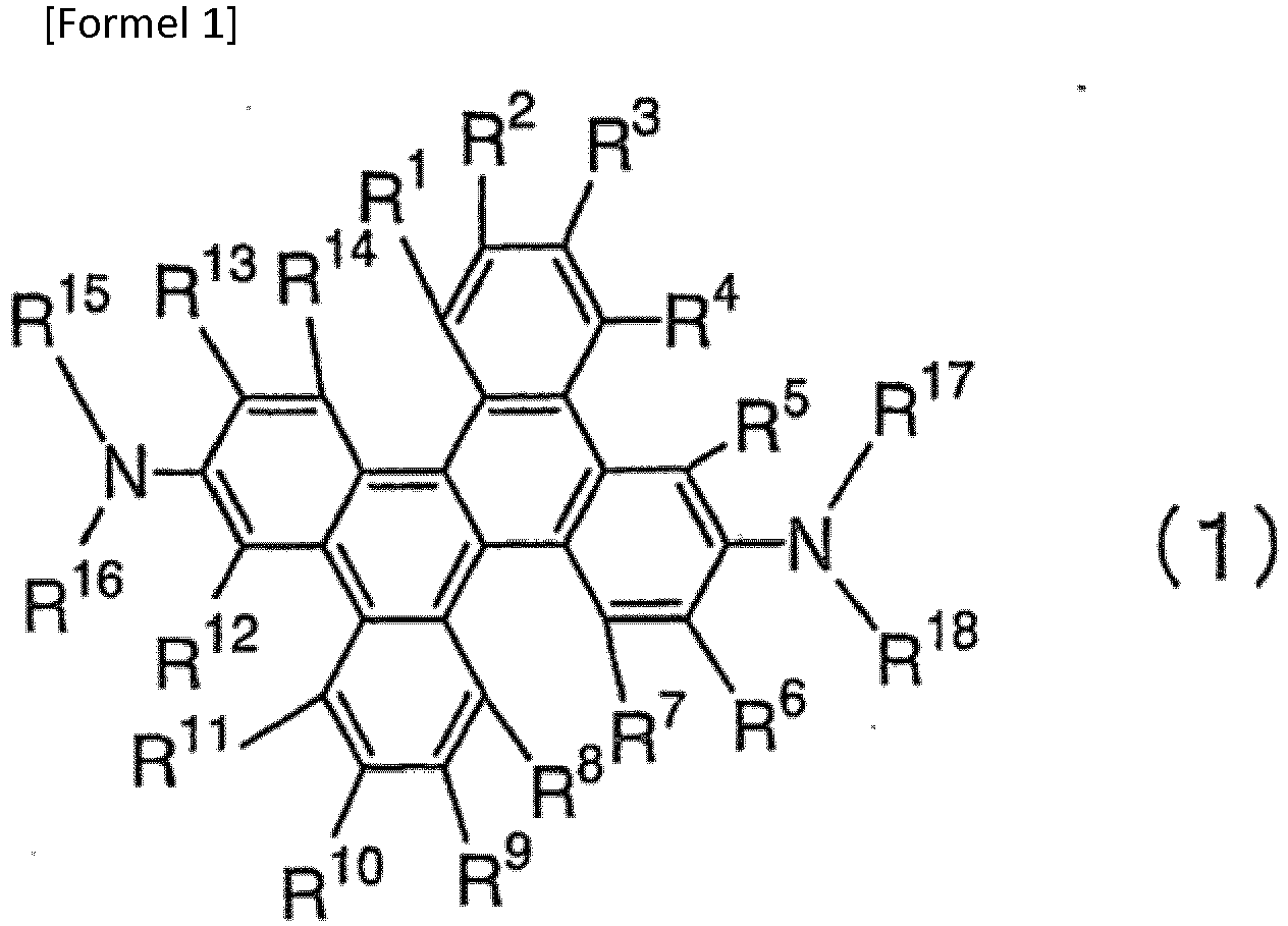
- a dibenzochrysene compound represented by the general formula (1) will be described in detail.
- the alkyl group represents a saturated aliphatic hydrocarbon group such as a methyl group, an ethyl group, an n-propyl group, an isopropyl group, an n-butyl group, a sec-butyl group or a tert-butyl group, and these alkyl groups may have a substituent or may have no substituent.
- An additional substituent in the case where the group is substituted is not particularly limited, and examples of the substituent include an alkyl group, an aryl group, and a heteroaryl group. This point is common to the following descriptions.
- the number of carbon atoms of the alkyl group is not particularly limited, but it is generally preferably 1 or more and 20 or less, and more preferably 1 or more and 8 or less from the viewpoint of ease of availability and cost.
- the cycloalkyl group represents a saturated alicyclic hydrocarbon group such as a cyclopropyl group, a cyclohexyl group, a norbornyl group or an adamantly group, and these cycloalkyl groups may have a substituent or may have no substituent.
- the number of carbon atoms of the cycloalkyl group is not particularly limited, but it is generally preferably 3 or more and 20 or less.
- the aryl group represents an aromatic hydrocarbon group such as a phenyl group, a naphthyl group, a biphenyl group, a phenanthryl group, a terphenyl group, a fluorenyl group, an anthracenyl group or a pyrenyl group.
- the aryl group may have a substituent or may have no substituent.
- the number of carbon atoms of the aryl group is not particularly limited, but it is generally preferably 6 or more and 40 or less.
- the heterocyclic group represents an aliphatic ring which has atoms other than carbon, such as a pyran ring, a piperidine ring and a cyclic amide in the ring, and these heterocyclic groups may have a substituent or may have no substituent.
- the number of carbon atoms of the heterocyclic group is not particularly limited, but it is generally preferably 2 or more and 20 or less.
- the heteroaryl group represents a cyclic aromatic group which has one or plural atoms other than carbon, such as a furanyl group, a thiophenyl group, a pyrrolyl group, a benzofuranyl group, a benzothiophenyl group, a dibenzofuranyl group, a dibenzothiophenyl group, a carbazolyl group, an indolyl group, a pyridyl group and a quinolinyl group in the ring, and these heteroaryl groups may have a substituent or may have no substituent.
- the number of carbon atoms of the heteroaryl group is not particularly limited, but it is generally preferably 2 or more and 30 or less.
- the heteroaryl group may be coupled to any position, and in the case of the pyridyl group, any form of a 2-pyridyl group, a 3-pyridyl group and a 4-pyridyl group may be employed.
- the alkenyl group represents unsaturated aliphatic hydrocarbon groups containing a double bond such as a vinyl group, an allyl group or a butadienyl group, and these alkenyl groups may have a substituent or may have no substituent.
- the number of carbon atoms of the alkenyl group is not particularly limited, but it is generally preferably 2 or more and 20 or less.
- the cycloalkenyl group represents an unsaturated alicyclic hydrocarbon groups containing a double bond such as a cyclopentenyl group, a cyclopentadienyl group or a cyclohexenyl group, and these cycloalkenyl groups may have a substituent or may have no substituent.
- the number of carbon atoms of the cycloalkenyl group is not particularly limited, but it is generally preferably 3 or more and 20 or less.
- the alkynyl group represents an unsaturated aliphatic hydrocarbon group containing a triple bond such as an ethynyl group, and these alkynyl groups may have a substituent or may have no substituent.
- the number of carbon atoms of the alkynyl group is not particularly limited, but it is generally preferably within the range of 2 or more and 20 or less.
- the alkoxy group represents a functional group formed by binding of aliphatic hydrocarbon groups with one another with an ether bond interposed therebetween such as a methoxy group, an ethoxy group or a propoxy group, and these aliphatic hydrocarbon groups may have a substituent or may have no substituent.
- the number of carbon atoms of the alkoxy group is not particularly limited, but it is generally preferably 1 or more and 20 or less.
- the alkylthio group represents a group formed by substitution of a sulfur atom for the oxygen atom of the ether bond of the alkoxy group.
- the hydrocarbon group of the alkylthio group may have a substituent or may have no substituent.
- the number of carbon atoms of the alkylthio group is not particularly limited, but it is generally preferably 1 or more and 20 or less.
- the aryl ether group represents a functional group formed by binding of aromatic hydrocarbon groups with one another with an ether bond interposed therebetween such as a phenoxy group, and these aromatic hydrocarbon groups may have a substituent or may have no substituent.
- the number of carbon atoms of the aryl ether group is not particularly limited, but it is generally preferably 6 or more and 40 or less.
- the arylthio ether group represents a group formed by substitution of a sulfur atom for the oxygen atom of the ether bond of the aryl ether group.
- An aromatic hydrocarbon group in the arylthio ether group may have a substituent or may have no substituent.
- the number of carbon atoms of the arylthio ether group is not particularly limited, but it is generally preferably 6 or more and 40 or less.
- Halogen represents fluorine, chlorine, bromine or iodine.
- R 19 and R 20 are each an aryl group or a heteroaryl group.
- the silyl group represents a functional group having a bond to a silicon atom such as a trimethylsilyl group or a triphenylsilyl group, and these silyl groups may have a substituent or may have no substituent.
- the number of carbon atoms of the silyl group is not particularly limited, but it is generally preferably 3 or more and 20 or less. Further, the number of silicon atoms of the silyl group is generally preferably 1 or more and 6 or less.
- fused ring formed between adjacent substituents when described with respect to the general formula (2), is a conjugated or nonconjugated fused ring formed between R 21 and R 22 .
- fused rings may contain a nitrogen, oxygen or sulfur atom in the ring structure, or may be coupled to another ring by condensation.
- R 1 to R 14 hydrogen, an alkyl group, a cycloalkyl group, an aryl group, a heteroaryl group, an alkoxy group, an aryl ether group and a silyl group are preferred as R 1 to R 14 .
- R 1 to R 14 is a sterically bulky substituent from the viewpoint of improvement in luminance efficiency and improvement in color purity, and for example, substituents such as an isopropyl group, a tert-butyl group, a cyclohexyl group, an adamantly group, a trimethylsilyl group and a triphenylsilyl group are preferred.
- an isopropyl group and a tert-butyl group are more preferred.
- the dibenzochrysene compound represented by the general formula (1) of the present invention is a light emitting device material which enables high luminance efficiency and excellent durability by introduction of two amino groups into a specific position of a dibenzochrysene skeleton. That is, the dibenzochrysene compound represented by the general formula (1) exhibits excellent performance such as high luminance efficiency, high color purity and a long life since the substitution position of the amino group is position-2 and position-10 of dibenzochrysene.
- the term light emitting device material refers to a compound involved in the emission in the light emitting device, and corresponds to either of a substance emitting light by itself and a substance assisting such a self-emitting substance to emit light.
- a hole injection material, a hole transporting material, an emissive material, an electron injection material and an electron transporting material correspond to the light emitting device material.
- the dibenzochrysene compound represented by the general formula (1) has excellent heat resistance and a high fluorescence quantum yield and exhibits intense emission in the blue region, it is suitably used particularly as a blue dopant material. By using the dibenzochrysene compound represented by the general formula (1) as the dopant material, it becomes possible to attain a light emitting device having high luminance efficiency and excellent durability.
- the dibenzochrysene compound represented by the general formula (1) has a dibenzochrysene skeleton, which is a large ⁇ -electron plane, as a main skeleton, a large hole transporting ability can be expected. Accordingly, the dibenzochrysene compound can be used as a hole transporting material or as a hole injection material. Furthermore, since the ionization potential in a state of an amorphous film of these compounds is about 5.0 to 5.6 eV, these compounds can be more suitably used as the hole injection material.
- R 15 to R 18 in the dibenzochrysene compound represented by the general formula (1) are each preferably an aryl group, and at least one of R 15 to R 18 is preferably a group represented by the general formula (2).
- each of R 21 to R 25 is selected from the group consisting of hydrogen, an aryl group, an alkyl group, a cycloalkyl group, an alkoxy group, an alkylthio group, an aryl ether group, an arylthio ether group, a silyl group and a fused ring formed between adjacent substituents, provided that at least one of R 21 to R 25 is an aryl group, an alkyl group or a cycloalkyl group, or at least one pair of groups adjacent to each other of R 21 to R 25 is a fused ring formed between adjacent substituents.
- a compound in which at least one of R 15 to R 18 is represented by the general formula (2) is synonymous with a compound represented by the following general formula (3).
- R 15 to R 18 is represented by the following general formula (4): wherein A is used for coupling with a nitrogen atom, each of R 21 to R 25 is selected from the group consisting of hydrogen, an aryl group, an alkyl group, a cycloalkyl group, an alkoxy group, an alkylthio group, an aryl ether group, an arylthio ether group, a silyl group and a fused ring formed between adjacent substituents, provided that at least one of R 21 to R 25 is an aryl group, an alkyl group or a cycloalkyl group, or at least one pair of groups adjacent to each other of R to R 25 is a fused ring formed between adjacent substituents.
- R 21 to R 25 is an aryl group, an alkyl group or a cycloalkyl group, or at least one pair of groups adjacent to each other of R 21 to R 25 is a fused ring formed between adjacent substituents
- the glass transition temperature of the dibenzochrysene compound represented by the general formula (1) or (3) is improved and more excellent heat resistance can be achieved. Further, these groups function as substituents of steric hindrance.
- the compound represented by the general formula (1) or (3) when used as a dopant, if the compound has such a substituent, the association between molecules of the dibenzochrysene compound represented by the general formula (1) or (3) or the association of the dibenzochrysene compound with a host compound is inhibited, concentration quenching and degradation of color purity can be suppressed, and a device having higher luminance efficiency can be obtained.
- An aryl group, an alkyl group and a cycloalkyl group are electron-donating groups and when at least one pair of groups adjacent to each other of R 21 to R 25 is a fused ring formed between adjacent substituents, the groups are also electron-donating groups. Therefore, when the compound represented by the general formula (1) or (3) is used as a hole injection material, if the compound has such a substituent, the ionization potential of the dibenzochrysene compound represented by the general formula (1) or (3) is decreased and therefore a hole is smoothly injected from an anode. As a result of this, the driving voltage of the light emitting device is reduced and consequently the effect of lengthening the life of the light emitting device is achieved.
- alkyl group or the cycloalkyl group of R 21 to R 25 include alkyl groups such as a methyl group, an ethyl group, an n-propyl group, an isopropyl group, an n-butyl group, a sec-butyl group and a tert-butyl group, and cycloalkyl groups such as a cyclopropyl group, a cyclohexyl group, a norbornyl group and an adamantly group.
- a sterically bulky substituent is preferred from the viewpoint of improvement in luminance efficiency and improvement in color purity, and an isopropyl group, a tert-butyl group, a cyclohexyl group, and an adamantly group are preferred. Furthermore, from the viewpoint of ease of availability of the raw material and relative ease of synthesis, an isopropyl group and a tert-butyl group are more preferred.
- the aryl groups of R 21 to R 25 are similar to those in the description of the general formula (1). However, since the wavelength of emission becomes long and color purity may deteriorate if an aryl group having the number of the fused rings of 3 or more is introduced, the aryl group of R 21 to R 25 is preferably an aryl group having the number of nucleus carbon atoms of 6 to 18 or an aromatic hydrocarbon group having the number of fused rings of 2 or less. Among these, a phenyl group, a biphenyl group, a fluorenyl group, a terphenyl group, and a naphthyl group are more preferred.
- examples of the case where at least one pair of groups adjacent to each other of R 21 to R 25 is a fused ring formed between adjacent substituents include a case where a group represented by the general formula (2) is consequently a naphthyl group, a fluorenyl group, an anthracenyl group or a pyrenyl group.
- the group represented by the general formula (2) is preferably a naphthyl group or a fluorenyl group.
- At least one of R 21 to R 25 is an alkyl group or a cycloalkyl group in order to particularly preferably improve both of the luminance efficiency and the color purity.
- alkyl group or the cycloalkyl group of R 21 to R 25 include alkyl groups such as a methyl group, an ethyl group, an n-propyl group, an isopropyl group, an n-butyl group, a sec-butyl group and a tert-butyl group, and cycloalkyl groups such as a cyclopropyl group, a cyclohexyl group, a norbornyl group and an adamantly group.
- a methyl group, an ethyl group, an n-propyl group, an isopropyl group, an n-butyl group, a tert-butyl group, a cyclohexyl group and an adamantly group are preferred.
- a methyl group, an ethyl group, an isopropyl group and a tert-butyl group are more preferred.
- the aryl groups of R 21 to R 25 are similar to those in the description of the general formula (1). However, since the wavelength of absorption becomes long to absorb emission from the emissive layer and luminance efficiency may deteriorate if an aryl group having the number of the fused rings of 3 or more is introduced, the aryl group of R 21 to R 25 is preferably an aryl group having the number of nucleus carbon atoms of 6 to 18 or an aromatic hydrocarbon group having the number of fused rings of 2 or less. Among these, a phenyl group, a biphenyl group, a fluorenyl group, a terphenyl group, and a naphthyl group are more preferred.
- examples of the case where at least one pair of groups adjacent to each other of R 21 to R 25 is a fused ring formed between adjacent substituents include a case where a group represented by the general formula (2) is consequently a naphthyl group, a fluorenyl group, an anthracenyl group or a pyrenyl group.
- the group represented by the general formula (2) is preferably a naphthyl group or a fluorenyl group.
- the dibenzochrysene compound represented by the general formula (1) or (3), described above, is not particularly limited, and specific examples thereof include the following compounds.
- a dimethoxy derivative of dibenzochrysene which is a main skeleton
- a method described in Journal of American Chemical Society (US), 2001, vol. 123, pp. 12087-12088 can be synthesized by a method described in Journal of American Chemical Society (US), 2001, vol. 123, pp. 12087-12088 .
- the methoxy group may be changed to a hydroxyl group and subsequently to triflate group, and the triflate derivative can be reacted with diarylamine by a coupling reaction using a palladium catalyst to obtain an objective compound, but the synthesis method of the compound is not limited to this method.
- the light emitting device of the present invention has an anode, a cathode, and an organic layer present there between, the organic layer contains at least an emissive layer, or contains a hole injection layer and an emissive layer, and the emissive layer emits light by electrical energy.
- the dibenzochrysene compound represented by the general formula (1) or (3) is contained in the organic layer.
- Examples of the constitution of the organic layer include lamination constitutions such as a hole transporting layer/an emissive layer, a hole transporting layer/an emissive layer/an electron transporting layer, a hole injection layer/a hole transporting layer/an emissive layer, and a hole injection layer/a hole transporting layer/an emissive layer/an electron transporting layer in addition to a constitution consisting only of an emissive layer.
- the above-described respective layers may be composed of a single layer or multiple layers.
- the electron transporting layer is composed of multiple layers, the layer on the side in contact with an electrode may be referred to as an electron injection layer, and the electron injection layer is included in the electron transporting layer in the following description.
- the material of the anode is not particularly limited as long as it is a material with which a hole can be efficiently injected into the organic layer, but a material having a relatively large work function is preferably used.
- the anode material include conductive metal oxides such as tin oxide, indium oxide, indium zinc oxide and indium tin oxide (ITO), metals such as gold, silver and chromium, inorganic conductive substances such as copper iodide and copper sulfide, and conductive polymers such as polythiophene, polypyrrole and polyaniline. These electrode materials may be used alone or by laminating or mixing a plurality of materials.
- the resistance of the anode is only required to supply a current sufficient for the emission of a light emitting device, but it is desirably low from the viewpoint of the power consumption of the light emitting device.
- the anode functions as an electrode, but it is particularly desirable to use a product with a low resistance of 100 ⁇ /square or lower.
- the thickness of the anode can be arbitrarily selected in accordance with the resistance value, but an anode of 100 to 300 nm in thickness is usually used.
- the anode is preferably formed on a substrate.
- a substrate of glass such as soda glass or alkali-free glass is suitably used.
- a thickness of 0.5 mm or more is enough since the glass substrate is only required to have an adequate thickness for maintaining the mechanical strength.
- the material of glass is more preferably alkali-free glass since less ion elution from glass is more preferable, but commercially available soda lime glass coated with a barrier coat such as SiO 2 can also be used.
- the material of the substrate does not have to be glass as long as the anode operates stably, and for example, the anode may be formed on a plastic substrate.
- the method of forming the anode is not particularly limited and, for example, an electron beam method, a sputtering method and a chemical reaction method can be employed.
- the material to be used for a cathode is not particularly limited as long as it is a material with which an electron can be efficiently injected into the organic layer, and examples of the material include platinum, gold, silver, copper, iron, tin, zinc, aluminum, indium, chromium, lithium, sodium, potassium, cesium, calcium and magnesium, and alloys thereof. In order to enhance the electron injection efficiency to improve device characteristics, lithium, sodium, potassium, cesium, calcium and magnesium, or alloys containing these metals of a low work function are effective.
- preferred examples of method for obtaining the cathode include a method for obtaining a highly stable electrode by doping the organic layer with a trace amount (the film thickness by vacuum evaporation is 1 nm or less in terms of a readout by a film thickness meter) of lithium or magnesium. Further, it is also possible to use inorganic salts such as lithium fluoride.
- metals such as platinum, gold, silver, copper, iron, tin, aluminum or indium or alloys using these metals, inorganic substances such as silica, titania or silicon nitride, and organic polymer compounds such as polyvinyl alcohol, polyvinyl chloride or hydrocarbon-based polymer compounds in order to protect the electrode.
- the method of forming the cathode is not particularly limited and for example, a resistance heating method, an electron beam method, a sputtering method, an ion plating method and a coating method can be used.
- a hole injection layer is formed by a method of laminating or mixing one species or two or more species of hole injection materials, or a method using a mixture of the hole injection material and a polymer binder. Further, the hole injection layer may be formed by adding an inorganic salt such as iron chloride (III) to the hole injection material. Further, a metal oxide such as molybdenum oxide or vanadium oxide may be added to the hole injection material to form a hole injection layer. Furthermore, the hole injection layer can also be formed by adding or laminating a compound having a strong accepting property such as a cyano group-substituted aromatic aza compound.
- a polymer having a function of injecting and transporting a hole may be dissolved in a solvent and a thin film may be formed from the resulting solution by a spin coating method or an ink-jet method.
- a Lewis acid such as iron chloride (III) or antimony chloride (V) may be added to the solution.
- the hole injection material is not particularly limited as long as it is a compound which can form a thin film and can transport a hole, and into which the hole can be smoothly injected from the anode.
- diphenylbenzidine derivatives such as 4,4'-bis(N-(3-methylphenyl)-N-phenylamino)biphenyl and 4,4'-bis(N-(1-naphthyl)-N-phenylamino)biphenyl
- triphenylamine derivatives such as 4,4',4" -tris(3-methylphenyl(phenyl)amino)triphenylamine
- biscarbazole derivatives such as bis(N-arylcarbazole) and bis(N-alkylcarbazole)
- heterocyclic compounds such as pyrazoline derivatives, stilbene compounds, hydrazone compounds, benzofuran derivatives, thiophene derivatives, oxadiazole derivatives, phthalocyanine derivatives and porphyrin derivatives
- polymers such as polycarbonate and styrene derivatives having the above-described monomers on the side chains, polythiophene,
- the dibenzochrysene compound represented by the general formula (1) or (3) of the present invention is used as a hole injection material, only one species of the dibenzochrysene compound may be used, or plural species of the dibenzochrysene compounds may be mixed and used. Further, the same technique as in the description of the hole injection layer described above, that is, the technique of mixing the metal oxide, the technique of adding or laminating a compound having a strong accepting property such as a cyano group-substituted aromatic aza compound, and the technique of adding a Lewis acid can be employed.
- a hole transporting layer is formed by a method of laminating or mixing one species or two or more species of hole transporting materials, or a method using a mixture of the hole transporting material and a polymer binder.
- the hole transporting material is not particularly limited as long as it is a compound which can form a thin film and can transport a hole, and into which the hole can be injected from the anode or the hole injection layer.
- diphenylbenzidine derivatives such as 4,4'-bis(N-(3-methylphenyl)-N-phenylamino)biphenyl and 4,4'-bis(N-(1-naphthyl)-N-phenylamino)biphenyl
- triphenylamine derivatives such as 4,4',4" -tris(3-methylphenyl(phenyl)amino)triphenylamine
- biscarbazole derivatives such as bis(N-arylcarbazole) and bis(N-alkylcarbazole)
- heterocyclic compounds such as pyrazoline derivatives, stilbene compounds, hydrazone compounds, benzofuran derivatives, thiophene derivatives and porphyrin derivatives
- polymers such as polycarbonate and styrene derivatives, having the above-described monomers on the side chains, polythiophene, polyaniline, polyfluorene, polyvinylc
- the emissive layer may be composed of a single layer or multiple layers, and both of the single layer and the multiple layers may be formed from a mixture of a host material and a dopant material or a host material alone.
- the host material and the dopant material may be respectively consist of one species or a plurality of species.
- the dopant material may be contained in the whole host material or may be partially contained in the host material.
- the dopant material and the host material may be laminated or the dopant material may be dispersed in the host material. Since the concentration quenching takes place when the amount of the dopant material is too large, this amount is preferably 20% by weight or less with respect to the total of the host material and the dopant material.
- the dopant material may be formed by co-evaporation of the dopant material and the host material, or the host material and the dopant material may be previously mixed before evaporation.
- the dibenzochrysene compound of the present invention may be used as a host material, but it is suitably used as a dopant material because of a high fluorescence quantum yield.
- the ionization potential of the dibenzochrysene compound represented by the general formula (1) or (3) of the present invention is not particularly limited, but the ionization potential is preferably 5 eV or more and 7 eV or less, more preferably 5.0 eV or more and 5.9 eV or less, and furthermore preferably 5.0 eV or more and 5.6 eV or less.
- the value of the ionization potential in the present invention was obtained by measuring a thin film, deposited on an ITO glass substrate in a thickness of 30 to 100 nm, with an atmospheric type ultraviolet photoelectron analyzing apparatus (AC-1, manufactured by RIKENKEIKI CO., LTD.).
- one species of the dibenzochrysene compound represented by the general formula (1) or (3) may be used, or plural species of the dibenzochrysene compounds may be mixed and used. Further, one or more species of other dopant materials may be mixed with the dibenzochrysene compound represented by the general formula (1) or (3).
- Examples of the dopant materials which can be mixed with the dibenzochrysene compound include compounds having an aryl ring such as naphthalene, anthracene, phenanthrene, pyrene, triphenylene, perylene, fluorene and indene, and derivatives thereof (for example, 2-(benzothiazole-2-yl)-9,10-diphenylanthracene and 5,6,11,12-tetraphenylnaphthacene); compounds having a heteroaryl ring such as furan, pyrrole, thiophene, silole, 9-silafluorene, 9,9'-spirobisilafluorene, benzothiophene, benzofuran, indole, dibenzothiophene, dibenzofuran, imidazopyridine, phenanthroline, pyrazine, naphthylidine, quinoxaline, pyrrolopyridine and thio
- the concentration of doping is preferably 20% by weight or less in order to suppress the concentration quenching, as described above.
- the concentration of doping is as low as 1% by weight or less, there is a possibility of adverse influence on the durability life of the device and therefore, it is more preferred to use the dibenzochrysene compound in a concentration in the range of 1 to 20% by weight.
- the host material contained in the emissive material is not particularly limited, but compounds having a condensed aryl ring such as anthracene and pyrene and derivatives thereof, aromatic amine derivatives such as N,N'-dinaphthyl-N,N'-diphenyl-4,4'-diphenyl-1,1'-diamine, metal-chelated oxinoid compounds including tris(8-guinolinato)aluminum (III), bisstyryl derivatives such as distyrylarylene derivatives, tetraphenylbutadiene derivatives, indene derivatives, coumarin derivatives, oxadiazole derivatives, pyrrolopyridine derivatives, perinone derivatives, cyclopentadiene derivatives, oxadiazole derivatives, carbazole derivatives, pyrrolopyrrole derivatives, and polymers such as polyphenylenevinylene derivatives, poly(p-phenylene) derivatives, polyfluorene
- derivatives are suitably used.
- an aromatic hydrocarbon derivative having an electron-donating property or a neutral substituent it is preferred because the effect of high luminance efficiency of the dibenzochrysene compound of the present invention is exhibited more remarkably.
- a compound selected from anthracene compounds, pyrene compounds and distyrylarylene compounds is used as a host material, it is preferred because the luminance efficiency is improved by a combination of this compound and the dibenzochrysene compound of the present invention.
- an anthracene compound or a pyrene compound having higher heat resistance and carrier-transporting capacity is combined with the dibenzochrysene compound of the present invention, it is more preferred since a light emitting device having high efficiency and a long life is obtained.
- the electron transporting layer is a layer into which an electron is injected from the cathode and which further transports the electron.
- the material to be used for the electron transporting layer is not particularly limited as long as it is a compound which has high electron injection efficiency and transports the injected electron efficiently.
- the material to be used for the electron transporting layer include compounds having a condensed aryl ring such as naphthalene and anthracene, and derivatives thereof; styryl-based aromatic ring derivatives typified by 4,4'-bis(diphenylethenyl)biphenyl, perylene derivatives, perynone derivatives, coumarin derivatives, naphthalimide derivatives, quinone derivatives such as anthraquinone and diphenoquinone, phosphorus oxide derivatives, carbazole derivatives and indole derivatives, quinolinol complexes such as tris(8-quinolinolato)aluminum(III), hydroxyazole complexes such as hydroxyphenyloxazole complex, azomethine complexes, tropolone metal complexes and flavonol metal complexes .
- the electron transporting material it is preferred to use a compound having a heteroaryl ring structure which is composed of
- the electron-accepting nitrogen refers to a nitrogen atom which forms a multiple bond between itself and an adjacent atom. Since the nitrogen atom has high electronegativity, the multiple bond has a property like an electron-accepting property and an excellent electron transporting capacity, and therefore by using the multiple bond for the electron transporting layer, the driving voltage of the light emitting device can be reduced. Thus, the heteroaryl ring including the electron-accepting nitrogen has high electron affinity.
- heteroaryl ring including the electron-accepting nitrogen examples include a pyridine ring, a pyrazine ring, a pyrimidine ring, a quinoline ring, a quinoxaline ring, a naphthyridine ring, a pyrimidopyrimidine ring, a benzoquinoline ring, a phenanthroline ring, an imidazole ring, an oxazole ring, an oxadiazole ring, a triazole ring, a thiazole ring, a thiadiazole ring, a benzoxazole ring, a benzothiazole ring, a benzimidazole ring, and a phenanthroimidazole ring.
- Examples of preferred compounds having the heteroaryl ring structure include benzimidazole derivatives, benzoxazole derivatives, benzothiazole derivatives, oxadiazole derivatives, thiadiazole derivatives, triazole derivatives, pyrazine derivatives, phenanthroline derivatives, quinoxaline derivatives, quinoline derivatives, benzoquinoline derivatives, oligopyridine derivatives such as bipyridine and terpyridine, quinoxaline derivatives, and naphthyridine derivatives.
- imidazole derivatives such as tris(N-phenylbenzimidazole-2-yl)benzene, oxadiazole derivatives such as 1,3-bis[(4-tert-butylphenyl)1,3,4-oxadiazoryl]phenylene, triazole derivatives such as N-naphthyl-2,5-diphenyl-1,3,4-triazole, phenanthroline derivatives such as bathocuproin and 1,3-bis(1,10-phenanthroline-9-yl)benzene, benzoquinoline derivatives such as 2,2'-bis(benzo[h]quinoline-2-yl)-9,9'-spirobifluorene, bipyridine derivatives such as 2,5-bis(6'-(2',2"-bipyridyl))-1,1-dimethyl-3,4-diphenylsil ole, terpyridine derivatives such as 1,3-bis(4'-(4'-(
- Particularly preferred examples include phenanthroline dimers such as 1,3-bis(1,10-phenanthroline-9-yl)benzene, 2,7-bis(1,10-phenanthroline-9-yl)naphthalene and 1,3-bis(2-phenyl-1,10-phenanthroline-9-yl)benzene, and bipyridine dimers such as 2,5-bis(6'-(2',2"-bipyridyl))-1,1-dimethyl-3,4-diphenylsil ole since the effect of improving luminance efficiency is significantly high when these dimers are combined with an emissive layer containing the dibenzochrysene compound represented by the general formula (1).
- phenanthroline dimers such as 1,3-bis(1,10-phenanthroline-9-yl)benzene, 2,7-bis(1,10-phenanthroline-9-yl)naphthalene and 1,3-bis(2-phenyl-1,10-phenanthroline-9-yl
- the above-described electron transporting materials may be used singly or as a mixture of two or more species thereof, or one or more other electron transporting materials may be mixed with the above-described electron transporting material. Further, the electron transporting material can be mixed with a metal such as an alkali metal or an alkaline earth metal.
- the ionization potential of the electron transporting layer is not particularly limited, but it is preferably 5.8 eV or more and 8.0 eV or less, and more preferably 6.0 eV or more and 7.5 eV or less.
- the method of forming the respective layers constituting the light emitting device is not particularly limited and examples thereof include a resistance heating evaporation method, an electron beam evaporation method, asputteringmethod, a molecular lamination method, a coating method, an ink-jet method, a printing method, and a laser-induced thermal transfer method.
- the resistance heating evaporation method or the electron beam evaporation method is preferred from the viewpoint of device characteristics.
- each of the layers cannot be limited since it depends on the resistance of the emissive substance, but it is selected from the range of 1 to 1000 nm.
- Film thicknesses of the emissive layer, the electron transporting layer and the hole transporting layer are respectively preferably 1 nm or more and 200 nm or less, and more preferably 5 nm or more and 100 nm or less.
- the light emitting device of the present invention has a function of converting electrical energy to light.
- the electrical energy a direct current is mainly used but a pulse current or an alternating current can also be used.
- the values of the current and the voltage are not particularly limited, but they are preferably selected so as to attain the maximum luminance with as low energy as possible in consideration of the power consumption and the life of the device.
- the light emitting device of the present invention is suitably used, for example, as displays displayed in a matrix system and/or segment system.
- the matrix system pixels for display are arrayed in a two-dimensional form such as a grid form or a mosaic form and a set of the pixels display characters and images.
- the shape and size of the pixel is determined according to the use. For example, for displaying images and characters on a personal computer, a monitor or a TV set, square pixels having a side of 300 ⁇ m or smaller are generally used, and in the case of a large display such as a display panel, pixels having a side of the order of millimeter are used.
- pixels having the same color may be arrayed, but in the case of color display, red, green and blue pixels are arrayed for display.
- a typical array system is a delta type or a stripe type.
- the method for driving this matrix may be either of passive matrix driving and active matrix driving.
- passive matrix driving the structure of the light emitting device is simple, but there may be cases where the active matrix driving is superior to the passive matrix driving in consideration of the operational characteristics.
- the driving method is switched depending on the application.
- the segment system is a system in which a pattern is formed so as to display predetermined information and an area defined by the layout of the pattern is made to emit light. Examples of this system include time indications or temperature indications in a digital clock or a digital thermometer, display of operational state of audio equipment or electromagnetic cookware, and an automobile panel display. Further, the matrix display and the segment display may co-exist in the same panel.
- the light emitting device of the present invention is also preferably used as backlights of various equipment.
- the backlight is predominantly used for the purpose of improving the visibility of a display which does not emit light spontaneously and used for a liquid crystal display, a clock, audio equipment, an automobile panel, a display board, and a sign.
- the light emitting device of the present invention is preferably used for a backlight for liquid crystal displays, particularly a backlight for personal computers for which thinning is investigated. With the light emitting device of the present invention, it is possible to provide a backlight of low-profile and lighter than the conventional backlights.
- the resulting organic layer was dried over magnesium sulfate and then the solvent was distilled off using a rotary evaporator.
- the resulting condensed product was purified by silica gel chromatography and recrystallized with hexane and then the crystal was vacuum-dried to obtain 13.3 g of the desired product (white crystal, yield 67.2%).
- the resulting organic layer was dried over magnesium sulfate and then the solvent was distilled off using a rotary evaporator.
- the resulting condensed product was purified by silica gel chromatography, and dispersed and washed with methanol and then the crystal was vacuum-dried to obtain 12.4 g of the desired product (light yellow crystal, yield 80.5%).
- the resulting organic layer was dried over magnesium sulfate and then the solvent was distilled off using a rotary evaporator, and the resulting solid was dispersed in a mixed liquid (mixing ratio 1 : 1) of acetone and methanol for washing and then the solid was vacuum-dried to obtain 4.1 g of the desired product (yellow crystal, yield 88.2%).
- reaction liquid was cooled to room temperature and extracted with 200 ml of dichloromethane, and separation/washing of the reaction liquid was carried out four times with 300 ml of distilled water.
- the resulting organic layer was dried over magnesium sulfate and then the solvent was distilled off using a rotary evaporator, and the resulting solid was purified by silica gel chromatography and vacuum-dried to obtain 6.3 g of the desired product (white crystal, yield 90.3%).
- Synthesis was performed under the same charge ratio, reaction condition, and purification condition as in Synthesis Example 1, (1-6) Synthesis of Compound [29] except for using 1 g of the intermediate E and bis(4-tert-butylphenyl)amine in place of p , p' -ditolylamine to obtain 1.15 g of the desired product (yellow crystal, yield 81.0%).
- This compound [39] was purified by sublimation at about 300°C at a pressure of 1.0 ⁇ 10 -3 Pa using an oil diffusion pump and then used as a light emitting device material.
- 1 H-NMR(CDCl 3 (d ppm))1.33(s, 36H), 7.10-7.40(m, 18H), 7.45-7.64(m, 4H), 8.23-8.67(m, 8H).
- a light emitting device using the compound [29] was prepared as follows.
- An ITO conductive film was formed in a thickness of 150 nm and a size of 30 ⁇ 13 mm on a central part of a glass substrate (produced by Asahi Glass Co., Ltd., 15 ⁇ /square, electron beam evaporation product) having a size of 30 ⁇ 40 mm to form an anode.
- the substrate provided with the anode was cleaned for 15 minutes through ultrasonic action by "SEMICOCLEAN (registered trade mark) 56" (manufactured by Furuuchi Chemical Corporation) and then cleaned with ultrapure water.
- the substrate was cleaned for 15 minutes in isopropyl alcohol through ultrasonic action, immersed for 15 minutes in hot methanol and dried.
- the substrate was treated in an atmosphere of UV-ozone for 1 hour immediately before preparing the device and then placed in a vacuum evaporation system, and the system was evacuated until the degree of vacuum in the system became 5 ⁇ 10 -5 Pa or less.
- Copper phthalocyanine as a hole injection material was first deposited in a thickness of 10 nm and 4,4'-bis(N-(1-naphthyl)-N-phenylamino)biphenyl as a hole transporting material was deposited in a thickness of 50 nm on the ITO film of the substrate by a resistance heating evaporation method.
- H-1 represented by the following formula was deposited as a host material of the emissive layer and the compound [29] was deposited in a thickness of 35 nm so as to have a doping concentration of 5% by weight as a dopant material.
- tris(8-quinolinolato)aluminum (Alq 3 ) as an electron transporting material was laminated in a thickness of 20 nm.
- Lithium fluoride was deposited in a thickness of 0.5 nm and aluminum was deposited in a thickness of 1000 nm on the organic layer thus formed to form a cathode to prepare a 5 mm square device.
- the film thickness referred to herein is an indicated value of a crystal oscillation type film thickness monitor.
- emission of high efficiency with a luminance efficiency of 3.2 lm/W and pure blue emission with CIE chromaticity coordinates of (0.14, 0.16) were achieved.
- the initial luminance of this device was set at 1000 cd/m 2 and the device was continuously driven with a direct current, and consequently the half-life of luminance was 2500 hours, indicating a long life.
- Light emitting devices were prepared in the same manner as in Example 1 except for using compounds shown in Table 1, respectively, as a dopant material, a host material of an emissive layer and an electron transporting material.
- the results of the luminance efficiency at the time of driving the device at a direct current of 10 mA/cm 2 , CIE chromaticity coordinates, and the half-life of luminance at the time when the initial luminance was set at 1000 cd/m 2 and the device was driven at a direct current are shown in Table 1.
- H-2, H-3, H-4, H-5, H-6, H-7, H-8 and H-9 represent compounds represented by the following formulas.
- Light emitting devices were prepared in the same manner as in Example 1 except for using compounds shown in Table 2, respectively, as a dopant material, a host material and an electron transporting material.
- Table 2 the results of the luminance efficiency at the time of driving the device at a direct current of 10 mA/cm 2 , CIE chromaticity coordinates, and the half-life of luminance at the time when the initial luminance was set at 1000 cd/m 2 and the device was driven at a direct current are shown in Table 2.
- the half-life of luminance of the device of Comparative Example 10 was not measured since the device exhibited poor color purity.
- D-1, D-2, D-3 and D-4 are compounds represented by the following formulas.
- Light emitting devices were prepared in the same manner as in Example 1 except for using compounds shown in Table 3, respectively, as a dopant material, a host material and an electron transporting material. With respect to these light emitting devices, the results of the luminance efficiency at the time of driving the device at a direct current of 10 mA/cm 2 , CIE chromaticity coordinates, and the half-life of luminance at the time when the initial luminance was set at 1000 cd/m 2 and the device was driven at a direct current are shown in Table 3.
- E-1, E-2, E-3, E-4 and E-5 are compounds represented by the following formulas.
- Light emitting devices were prepared in the same manner as in Example 1 except for using compounds shown in Table 3, respectively, as a dopant material, a host material and an electron transporting material. With respect to these light emitting devices, the results of the luminance efficiency at the time of driving the device at a direct current of 10 mA/cm 2 , CIE chromaticity coordinates, and the half-life of luminance at the time when the initial luminance was set at 1000 cd/m 2 and the device was driven at a direct current are shown in Table 3.
- a light emitting device using the compound [29] as a hole injection material was prepared as follows.
- An ITO conductive film was formed in a thickness of 150 nm and a size of 30 x 13 mm on a central part of a glass substrate (produced by Asahi Glass Co., Ltd. , 15 ⁇ /square, electron beam evaporation product) having a size of 30 x 40 mm to form an anode.
- the substrate provided with the anode was cleaned for 15 minutes through ultrasonic action by "SEMICOCLEAN (registered trade mark) 56" (manufactured by Furuuchi Chemical Corporation) and then cleaned with ultrapure water.
- the substrate was cleaned for 15 minutes in isopropyl alcohol through ultrasonic action, immersed for 15 minutes in hot methanol and dried.
- the substrate was treated in an atmosphere of UV-ozone for 1 hour immediately before preparing the device and then placed in a vacuum evaporation system, and the system was evacuated until the degree of vacuum in the system became 5 ⁇ 10 -5 Pa or less.
- the compound [29] as a hole injection material was first deposited in a thickness of 40 nm and 4,4'-bis(N-(1-naphthyl)-N-phenylamino)biphenyl as a hole transporting material was deposited in a thickness of 10 nm on the ITO film of the substrate by a resistance heating evaporation method.
- H-1 was deposited as a host material of the emissive layer and D-4 was deposited in a thickness of 35 nm so as to have a doping concentration of 5% by weight as a dopant material.
- tris(8-quinolinolato)aluminum (Alq 3 ) as an electron transporting material was laminated in a thickness of 20 nm.
- Lithium fluoride was deposited in a thickness of 0.5 nm and aluminum was deposited in a thickness of 1000 nm on the organic layer thus formed to form a cathode to prepare a 5 mm square device.
- the film thickness referred to herein is an indicated value of a crystal oscillation type film thickness monitor.
- emission of high efficiency with a luminance efficiency of 3.5 lm/W and pure blue emission with CIE chromaticity coordinates of (0.14, 0.14) were achieved.
- the initial luminance of this device was set at 1000 cd/m 2 and the device was continuously driven with a direct current, and consequently the half-life of luminance was 2500 hours, indicating a long life.
- Light emitting devices were prepared in the same manner as in Example 55 except for using compounds shown in Table 4, respectively, as a hole injection material, a host material and a dopant material. With respect to these light emitting devices, the results of the luminance efficiency at the time of driving the device at a direct current of 10 mA/cm 2 , CIE chromaticity coordinates, and a half-life of luminance at the time when the initial luminance was set at 1000 cd/m 2 and the device was driven at a direct current are shown in Table 4.
- Light emitting devices were prepared in the same manner as in Example 55 except for using compounds shown in Table 4, respectively, as a hole injection material, a host material and a dopant material. With respect to these light emitting devices , the results of the luminance efficiency at the time of driving the device at a direct current of 10 mA/cm 2 , CIE chromaticity coordinates, and the half-life of luminance at the time when the initial luminance was set at 1000 cd/m 2 and the device was driven at a direct current are shown in Table 4.
- HI-1 and HI-2 are compounds represented by the following formulas.
- Light emitting devices were prepared in the same manner as in Example 55 except for using compounds shown in Table 5, respectively, as a hole injection material, a host material and a dopant material. With respect to these light emitting devices, the results of the luminance efficiency at the time of driving the device at a direct current of 10 mA/cm 2 , CIE chromaticity coordinates, and the half-life of luminance at the time when the initial luminance was set at 1000 cd/m 2 and the device was driven at a direct current are shown in Table 5.
- Light emitting devices were prepared in the same manner as in Example 55 except for using compounds shown in Table 6, respectively, as a hole injection material, a host material and a dopant material. With respect to these light emitting devices, the results of the luminance efficiency at the time of driving the device at a direct current of 10 mA/cm 2 , CIE chromaticity coordinates, and the half-life of luminance at the time when the initial luminance was set at 1000 cd/m 2 and the device was driven at a direct current are shown in Table 6.
- Light emitting devices were prepared in the same manner as in Example 55 except for using compounds shown in Table 7, respectively, as a hole injection material, a host material, a dopant material and an electron transporting material. With respect to these light emitting devices, the results of the luminance efficiency at the time of driving the device at a direct current of 10 mA/cm 2 , CIE chromaticity coordinates, and the half-life of luminance at the time when the initial luminance was set at 1000 cd/m 2 and the device was driven at a direct current are shown in Table 7.
- Light emitting devices were prepared in the same manner as in Example 55 except for using compounds shown in Table 7, respectively, as a hole injection material, a host material, a dopant material and an electron transporting material. With respect to these light emitting devices, the results of the luminance efficiency at the time of driving the device at a direct current of 10 mA/cm 2 , CIE chromaticity coordinates, and the half-life of luminance at the time when the initial luminance was set at 1000 cd/m 2 and the device was driven at a direct current are shown in Table 7.
- the light emitting device material of the present invention can be used for light emitting devices and can provide a light emitting device material which is excellent in thin film stability.
- the light emitting device of the present invention can be used for the fields of display devices, flat panel displays, backlights, illumination, interior decoration, signs, signboards, electron cameras and optical signal generators.
Landscapes
- Chemical & Material Sciences (AREA)
- Engineering & Computer Science (AREA)
- Materials Engineering (AREA)
- Organic Chemistry (AREA)
- Physics & Mathematics (AREA)
- Spectroscopy & Molecular Physics (AREA)
- Optics & Photonics (AREA)
- Electroluminescent Light Sources (AREA)
Claims (9)
- Lichtemittierendes Vorrichtungsmaterial, welches für eine lichtemittierende Vorrichtung verwendet wird, welches mindestens eine emissive Schicht mit einem Wirtsmaterial und einem Dotiermaterial aufweist und zwischen einer Anode und einer Kathode vorhanden ist und Licht durch elektrische Energie emittiert, wobei das lichtemittierende Vorrichtungsmaterial ein lichtemittierendes Vorrichtungsmaterial für ein Dotiermaterial mit einem Dibenzochrysengerüst, welches durch die allgemeine Formel (1) dargestellt ist, ist:
- Lichtemittierendes Vorrichtungsmaterial nach Anspruch 1, wobei mindestens einer von R15 bis R18 durch die folgende allgemeine Formel (2) dargestellt ist:

- Lichtemittierendes Vorrichtungsmaterial nach Anspruch 2, wobei mindestens einer von R21 bis R25 eine Alkylgruppe oder eine Cycloalkylgruppe ist.
- Lichtemittierendes Vorrichtungsmaterial nach Anspruch 1, wobei R15 bis R18 eine Arylgruppe ist, und wobei mindestens einer von R15 bis R18 durch die folgende allgemeine Formel (4) dargestellt ist:

- Verwendung des lichtemittierenden Vorrichtungsmaterials nach Anspruch 4 als ein Löcherinjektionsmaterial in einer lichtemittierenden Vorrichtung umfassend mindestens eine Löcherinjektionsschicht und eine emissive Schicht, welche zwischen einer Anode und einer Kathode vorhanden ist und Licht durch elektrische Anregung emittiert.
- Lichtemittierende Vorrichtung umfassend mindestens eine Löcherinjektionsschicht und eine emissive Schicht, welche zwischen einer Anode und einer Kathode vorhanden ist und Licht durch elektrische Energie emittiert, wobei das lichtemittierende Vorrichtungsmaterial nach Anspruch 4 in der Löcherinjektionsschicht enthalten ist.
- Lichtemittierende Vorrichtung umfassend mindestens eine emissive Schicht, welche zwischen der Anode und der Kathode vorhanden ist und Licht durch elektrische Energie emittiert, wobei die emissive Schicht ein Wirtsmaterial und ein Dotiermaterial aufweist und das lichtemittierende Vorrichtungsmaterial nach einem der Ansprüche 1 bis 3 als das Dotierungsmittel enthält.
- Lichtemittierende Vorrichtung nach Anspruch 7, wobei das Wirtsmaterial ausgewählt ist aus einer Anthracenverbindung und einer Pyrenverbindung.
- Lichtemittierende Vorrichtung nach einem der Ansprüche 6 bis 8, wobei mindestens eine Elektronentransportschicht zwischen der emissiven Schicht und der Kathode vorhanden ist, und die Elektronentransportschicht elektronenakzeptierenden Stickstoff enthält und eine Verbindung mit einer Heteroarylringstruktur, welche sich aus Elementen ausgewählt aus Kohlenstoff, Wasserstoff, Stickstoff, Sauerstoff, Silicium und Phosphor zusammensetzt, enthält.
Applications Claiming Priority (2)
| Application Number | Priority Date | Filing Date | Title |
|---|---|---|---|
| JP2008045622 | 2008-02-27 | ||
| PCT/JP2009/052961 WO2009107549A1 (ja) | 2008-02-27 | 2009-02-20 | 発光素子材料および発光素子 |
Publications (3)
| Publication Number | Publication Date |
|---|---|
| EP2248868A1 EP2248868A1 (de) | 2010-11-10 |
| EP2248868A4 EP2248868A4 (de) | 2015-05-06 |
| EP2248868B1 true EP2248868B1 (de) | 2018-09-19 |
Family
ID=41015946
Family Applications (1)
| Application Number | Title | Priority Date | Filing Date |
|---|---|---|---|
| EP09714824.1A Not-in-force EP2248868B1 (de) | 2008-02-27 | 2009-02-20 | Leuchtstoffmaterial und leuchstoffelement |
Country Status (6)
| Country | Link |
|---|---|
| EP (1) | EP2248868B1 (de) |
| JP (1) | JP4968333B2 (de) |
| KR (1) | KR101807644B1 (de) |
| CN (1) | CN101939401B (de) |
| TW (1) | TWI443176B (de) |
| WO (1) | WO2009107549A1 (de) |
Families Citing this family (15)
| Publication number | Priority date | Publication date | Assignee | Title |
|---|---|---|---|---|
| JP5685832B2 (ja) * | 2009-05-29 | 2015-03-18 | Jnc株式会社 | ジベンゾ[g,p]クリセン化合物、該化合物を含有する発光層用材料、およびこれを用いた有機電界発光素子 |
| JP5578996B2 (ja) * | 2009-09-11 | 2014-08-27 | 富士フイルム株式会社 | 光電変換素子及びその製造方法、光センサ、並びに撮像素子及びそれらの駆動方法 |
| WO2012002245A1 (ja) * | 2010-07-02 | 2012-01-05 | コニカミノルタホールディングス株式会社 | 有機エレクトロルミネッセンス素子 |
| KR101990024B1 (ko) * | 2011-04-15 | 2019-06-17 | 에스에프씨 주식회사 | 디벤조크리센 유도체 화합물 및 이를 포함하는 유기전계발광소자 |
| KR20140037826A (ko) * | 2011-06-23 | 2014-03-27 | 도레이 카부시키가이샤 | 발광 소자 |
| JP2014167946A (ja) * | 2011-06-23 | 2014-09-11 | Toray Ind Inc | 発光素子 |
| KR102316681B1 (ko) * | 2015-01-09 | 2021-10-26 | 삼성디스플레이 주식회사 | 화합물 및 이를 포함하는 유기 발광 소자 |
| US11730053B2 (en) | 2015-05-06 | 2023-08-15 | Samsung Display Co., Ltd. | Organic light-emitting device |
| US10147884B2 (en) | 2015-05-06 | 2018-12-04 | Samsung Display Co., Ltd. | Organic light-emitting device |
| JP7135428B2 (ja) * | 2017-05-17 | 2022-09-13 | 東ソー株式会社 | 縮合環化合物 |
| KR101876763B1 (ko) * | 2017-05-22 | 2018-07-11 | 머티어리얼사이언스 주식회사 | 유기화합물 및 이를 포함하는 유기전계발광소자 |
| JP7234532B2 (ja) * | 2017-08-18 | 2023-03-08 | 東ソー株式会社 | ジベンゾ[g,p]クリセン化合物 |
| JP7236896B2 (ja) * | 2019-03-25 | 2023-03-10 | 東ソー株式会社 | 縮合環化合物の製造方法 |
| CN110128282B (zh) * | 2019-04-24 | 2022-04-26 | 南京邮电大学 | 一种二苯并屈类衍生物及其用途 |
| EP4613746A3 (de) | 2021-06-11 | 2025-11-19 | Tosoh Corporation | Photoelektrisches umwandlungselement für ein bilderzeugungselement |
Family Cites Families (13)
| Publication number | Priority date | Publication date | Assignee | Title |
|---|---|---|---|---|
| JPH0517765A (ja) | 1991-07-16 | 1993-01-26 | Idemitsu Kosan Co Ltd | 有機エレクトロルミネツセンス素子 |
| JP2873548B2 (ja) | 1995-04-21 | 1999-03-24 | バンドー化学株式会社 | 新規なトリフェニルアミン化合物 |
| JP4542646B2 (ja) | 1998-09-09 | 2010-09-15 | 出光興産株式会社 | 有機エレクトロルミネッセンス素子およびフェニレンジアミン誘導体 |
| WO2000027946A1 (en) * | 1998-11-11 | 2000-05-18 | Kabushiki Kaisha Toyota Chuo Kenkyusho | Organic electroluminescent element |
| JP2001326079A (ja) * | 2000-05-17 | 2001-11-22 | Toyota Central Res & Dev Lab Inc | 有機電界発光素子 |
| JP4838969B2 (ja) | 2000-09-01 | 2011-12-14 | 出光興産株式会社 | 新規スチリル化合物及び有機エレクトロルミネッセンス素子 |
| JP2002237384A (ja) * | 2001-02-07 | 2002-08-23 | Toyota Central Res & Dev Lab Inc | 有機電界発光素子 |
| EP1541657B2 (de) * | 2002-07-19 | 2014-03-05 | Idemitsu Kosan Co., Ltd. | Organische elektrolumineszenzvorrichtungen und organisches lumineszenzmedium |
| CN1978586A (zh) | 2002-11-12 | 2007-06-13 | 出光兴产株式会社 | 用于有机电致发光器件的材料和使用该材料的有机电致发光器件 |
| US6830833B2 (en) * | 2002-12-03 | 2004-12-14 | Canon Kabushiki Kaisha | Organic light-emitting device based on fused conjugated compounds |
| EP1604974A4 (de) | 2003-03-20 | 2007-11-14 | Idemitsu Kosan Co | Aromatische aminderivate und unter verwendung dieser hergestelltes organisches elektrolumineszentes element |
| JP2005302667A (ja) * | 2004-04-15 | 2005-10-27 | Idemitsu Kosan Co Ltd | 有機エレクトロルミネッセンス素子 |
| JP2007230960A (ja) * | 2006-03-03 | 2007-09-13 | Idemitsu Kosan Co Ltd | 芳香族アミン誘導体及びそれを用いた有機エレクトロルミネッセンス素子 |
-
2009
- 2009-02-20 KR KR1020107015523A patent/KR101807644B1/ko not_active Expired - Fee Related
- 2009-02-20 CN CN2009801046090A patent/CN101939401B/zh not_active Expired - Fee Related
- 2009-02-20 WO PCT/JP2009/052961 patent/WO2009107549A1/ja not_active Ceased
- 2009-02-20 JP JP2009513149A patent/JP4968333B2/ja not_active Expired - Fee Related
- 2009-02-20 EP EP09714824.1A patent/EP2248868B1/de not_active Not-in-force
- 2009-02-25 TW TW098105896A patent/TWI443176B/zh not_active IP Right Cessation
Non-Patent Citations (1)
| Title |
|---|
| None * |
Also Published As
| Publication number | Publication date |
|---|---|
| KR20100115738A (ko) | 2010-10-28 |
| TWI443176B (zh) | 2014-07-01 |
| JPWO2009107549A1 (ja) | 2011-06-30 |
| EP2248868A4 (de) | 2015-05-06 |
| WO2009107549A1 (ja) | 2009-09-03 |
| KR101807644B1 (ko) | 2017-12-11 |
| TW200940682A (en) | 2009-10-01 |
| JP4968333B2 (ja) | 2012-07-04 |
| CN101939401B (zh) | 2013-10-02 |
| EP2248868A1 (de) | 2010-11-10 |
| CN101939401A (zh) | 2011-01-05 |
Similar Documents
| Publication | Publication Date | Title |
|---|---|---|
| EP2416396B1 (de) | Material für ein lichtemittierendes element und lichtemittierendes element | |
| EP1942171B1 (de) | Material für ein lichtemittierendes gerät und lichtemittierendes gerät | |
| EP2296204B1 (de) | Lichtemittierendes element | |
| EP2709181B1 (de) | Material für ein lichtemittierendes element und lichtemittierendes element | |
| EP2028249B1 (de) | Material für eine lichtemittierende vorrichtung und lichtemittierende vorrichtung | |
| EP2248868A1 (de) | Leuchtstoffmaterial und leuchstofftelement | |
| CN102272971B (zh) | 发光元件材料和发光元件 | |
| EP2722905B1 (de) | Material für ein lichtemittierendes element und lichtemittierendes element | |
| KR101204132B1 (ko) | 발광 소자 재료 및 발광 소자 | |
| EP1748045A1 (de) | Material für ein lichtemittierendes gerät und lichtemittierendes gerät | |
| KR102028940B1 (ko) | 발광 소자 재료 및 발광 소자 | |
| KR20140098050A (ko) | 벤조플루오렌 화합물, 그 화합물을 사용한 발광층용 재료 및 유기 전계 발광 소자 | |
| JP6269060B2 (ja) | 発光素子材料および発光素子 | |
| EP2172534B1 (de) | Material für eine lichtemittierende vorrichtung und lichtemittierende vorrichtung | |
| EP2871686B1 (de) | Material für ein lichtemittierendes element und lichtemittierendes element | |
| JP5402128B2 (ja) | ビピリジル基を有するアントラセンまたはナフタレン誘導体化合物および有機電界発光素子 | |
| JP5194649B2 (ja) | 発光素子材料および発光素子 | |
| JP2009096946A (ja) | 発光素子材料および発光素子 |
Legal Events
| Date | Code | Title | Description |
|---|---|---|---|
| PUAI | Public reference made under article 153(3) epc to a published international application that has entered the european phase |
Free format text: ORIGINAL CODE: 0009012 |
|
| 17P | Request for examination filed |
Effective date: 20100812 |
|
| AK | Designated contracting states |
Kind code of ref document: A1 Designated state(s): AT BE BG CH CY CZ DE DK EE ES FI FR GB GR HR HU IE IS IT LI LT LU LV MC MK MT NL NO PL PT RO SE SI SK TR |
|
| AX | Request for extension of the european patent |
Extension state: AL BA RS |
|
| DAX | Request for extension of the european patent (deleted) | ||
| RA4 | Supplementary search report drawn up and despatched (corrected) |
Effective date: 20150409 |
|
| RIC1 | Information provided on ipc code assigned before grant |
Ipc: H01L 51/50 20060101ALI20150401BHEP Ipc: C09K 11/06 20060101AFI20150401BHEP Ipc: C07C 211/61 20060101ALI20150401BHEP |
|
| STAA | Information on the status of an ep patent application or granted ep patent |
Free format text: STATUS: EXAMINATION IS IN PROGRESS |
|
| 17Q | First examination report despatched |
Effective date: 20171120 |
|
| GRAJ | Information related to disapproval of communication of intention to grant by the applicant or resumption of examination proceedings by the epo deleted |
Free format text: ORIGINAL CODE: EPIDOSDIGR1 |
|
| GRAP | Despatch of communication of intention to grant a patent |
Free format text: ORIGINAL CODE: EPIDOSNIGR1 |
|
| GRAP | Despatch of communication of intention to grant a patent |
Free format text: ORIGINAL CODE: EPIDOSNIGR1 |
|
| STAA | Information on the status of an ep patent application or granted ep patent |
Free format text: STATUS: GRANT OF PATENT IS INTENDED |
|
| RIC1 | Information provided on ipc code assigned before grant |
Ipc: H01L 51/50 20060101ALI20180329BHEP Ipc: C07C 211/61 20060101ALI20180329BHEP Ipc: C09K 11/06 20060101AFI20180329BHEP Ipc: H01L 51/00 20060101ALI20180329BHEP |
|
| INTG | Intention to grant announced |
Effective date: 20180419 |
|
| GRAS | Grant fee paid |
Free format text: ORIGINAL CODE: EPIDOSNIGR3 |
|
| GRAA | (expected) grant |
Free format text: ORIGINAL CODE: 0009210 |
|
| STAA | Information on the status of an ep patent application or granted ep patent |
Free format text: STATUS: THE PATENT HAS BEEN GRANTED |
|
| AK | Designated contracting states |
Kind code of ref document: B1 Designated state(s): AT BE BG CH CY CZ DE DK EE ES FI FR GB GR HR HU IE IS IT LI LT LU LV MC MK MT NL NO PL PT RO SE SI SK TR |
|
| REG | Reference to a national code |
Ref country code: GB Ref legal event code: FG4D |
|
| REG | Reference to a national code |
Ref country code: CH Ref legal event code: EP |
|
| REG | Reference to a national code |
Ref country code: AT Ref legal event code: REF Ref document number: 1043239 Country of ref document: AT Kind code of ref document: T Effective date: 20181015 |
|
| REG | Reference to a national code |
Ref country code: IE Ref legal event code: FG4D |
|
| REG | Reference to a national code |
Ref country code: DE Ref legal event code: R096 Ref document number: 602009054583 Country of ref document: DE |
|
| REG | Reference to a national code |
Ref country code: NL Ref legal event code: MP Effective date: 20180919 |
|
| PG25 | Lapsed in a contracting state [announced via postgrant information from national office to epo] |
Ref country code: FI Free format text: LAPSE BECAUSE OF FAILURE TO SUBMIT A TRANSLATION OF THE DESCRIPTION OR TO PAY THE FEE WITHIN THE PRESCRIBED TIME-LIMIT Effective date: 20180919 Ref country code: NO Free format text: LAPSE BECAUSE OF FAILURE TO SUBMIT A TRANSLATION OF THE DESCRIPTION OR TO PAY THE FEE WITHIN THE PRESCRIBED TIME-LIMIT Effective date: 20181219 Ref country code: SE Free format text: LAPSE BECAUSE OF FAILURE TO SUBMIT A TRANSLATION OF THE DESCRIPTION OR TO PAY THE FEE WITHIN THE PRESCRIBED TIME-LIMIT Effective date: 20180919 Ref country code: BG Free format text: LAPSE BECAUSE OF FAILURE TO SUBMIT A TRANSLATION OF THE DESCRIPTION OR TO PAY THE FEE WITHIN THE PRESCRIBED TIME-LIMIT Effective date: 20181219 Ref country code: GR Free format text: LAPSE BECAUSE OF FAILURE TO SUBMIT A TRANSLATION OF THE DESCRIPTION OR TO PAY THE FEE WITHIN THE PRESCRIBED TIME-LIMIT Effective date: 20181220 Ref country code: LT Free format text: LAPSE BECAUSE OF FAILURE TO SUBMIT A TRANSLATION OF THE DESCRIPTION OR TO PAY THE FEE WITHIN THE PRESCRIBED TIME-LIMIT Effective date: 20180919 |
|
| REG | Reference to a national code |
Ref country code: LT Ref legal event code: MG4D |
|
| PG25 | Lapsed in a contracting state [announced via postgrant information from national office to epo] |
Ref country code: LV Free format text: LAPSE BECAUSE OF FAILURE TO SUBMIT A TRANSLATION OF THE DESCRIPTION OR TO PAY THE FEE WITHIN THE PRESCRIBED TIME-LIMIT Effective date: 20180919 Ref country code: HR Free format text: LAPSE BECAUSE OF FAILURE TO SUBMIT A TRANSLATION OF THE DESCRIPTION OR TO PAY THE FEE WITHIN THE PRESCRIBED TIME-LIMIT Effective date: 20180919 |
|
| REG | Reference to a national code |
Ref country code: AT Ref legal event code: MK05 Ref document number: 1043239 Country of ref document: AT Kind code of ref document: T Effective date: 20180919 |
|
| PG25 | Lapsed in a contracting state [announced via postgrant information from national office to epo] |
Ref country code: ES Free format text: LAPSE BECAUSE OF FAILURE TO SUBMIT A TRANSLATION OF THE DESCRIPTION OR TO PAY THE FEE WITHIN THE PRESCRIBED TIME-LIMIT Effective date: 20180919 Ref country code: NL Free format text: LAPSE BECAUSE OF FAILURE TO SUBMIT A TRANSLATION OF THE DESCRIPTION OR TO PAY THE FEE WITHIN THE PRESCRIBED TIME-LIMIT Effective date: 20180919 Ref country code: IS Free format text: LAPSE BECAUSE OF FAILURE TO SUBMIT A TRANSLATION OF THE DESCRIPTION OR TO PAY THE FEE WITHIN THE PRESCRIBED TIME-LIMIT Effective date: 20190119 Ref country code: PL Free format text: LAPSE BECAUSE OF FAILURE TO SUBMIT A TRANSLATION OF THE DESCRIPTION OR TO PAY THE FEE WITHIN THE PRESCRIBED TIME-LIMIT Effective date: 20180919 Ref country code: CZ Free format text: LAPSE BECAUSE OF FAILURE TO SUBMIT A TRANSLATION OF THE DESCRIPTION OR TO PAY THE FEE WITHIN THE PRESCRIBED TIME-LIMIT Effective date: 20180919 Ref country code: RO Free format text: LAPSE BECAUSE OF FAILURE TO SUBMIT A TRANSLATION OF THE DESCRIPTION OR TO PAY THE FEE WITHIN THE PRESCRIBED TIME-LIMIT Effective date: 20180919 Ref country code: EE Free format text: LAPSE BECAUSE OF FAILURE TO SUBMIT A TRANSLATION OF THE DESCRIPTION OR TO PAY THE FEE WITHIN THE PRESCRIBED TIME-LIMIT Effective date: 20180919 Ref country code: AT Free format text: LAPSE BECAUSE OF FAILURE TO SUBMIT A TRANSLATION OF THE DESCRIPTION OR TO PAY THE FEE WITHIN THE PRESCRIBED TIME-LIMIT Effective date: 20180919 Ref country code: IT Free format text: LAPSE BECAUSE OF FAILURE TO SUBMIT A TRANSLATION OF THE DESCRIPTION OR TO PAY THE FEE WITHIN THE PRESCRIBED TIME-LIMIT Effective date: 20180919 |
|
| PG25 | Lapsed in a contracting state [announced via postgrant information from national office to epo] |
Ref country code: SK Free format text: LAPSE BECAUSE OF FAILURE TO SUBMIT A TRANSLATION OF THE DESCRIPTION OR TO PAY THE FEE WITHIN THE PRESCRIBED TIME-LIMIT Effective date: 20180919 Ref country code: PT Free format text: LAPSE BECAUSE OF FAILURE TO SUBMIT A TRANSLATION OF THE DESCRIPTION OR TO PAY THE FEE WITHIN THE PRESCRIBED TIME-LIMIT Effective date: 20190119 |
|
| REG | Reference to a national code |
Ref country code: DE Ref legal event code: R097 Ref document number: 602009054583 Country of ref document: DE |
|
| PLBE | No opposition filed within time limit |
Free format text: ORIGINAL CODE: 0009261 |
|
| STAA | Information on the status of an ep patent application or granted ep patent |
Free format text: STATUS: NO OPPOSITION FILED WITHIN TIME LIMIT |
|
| PG25 | Lapsed in a contracting state [announced via postgrant information from national office to epo] |
Ref country code: DK Free format text: LAPSE BECAUSE OF FAILURE TO SUBMIT A TRANSLATION OF THE DESCRIPTION OR TO PAY THE FEE WITHIN THE PRESCRIBED TIME-LIMIT Effective date: 20180919 |
|
| 26N | No opposition filed |
Effective date: 20190620 |
|
| REG | Reference to a national code |
Ref country code: CH Ref legal event code: PL |
|
| GBPC | Gb: european patent ceased through non-payment of renewal fee |
Effective date: 20190220 |
|
| PG25 | Lapsed in a contracting state [announced via postgrant information from national office to epo] |
Ref country code: SI Free format text: LAPSE BECAUSE OF FAILURE TO SUBMIT A TRANSLATION OF THE DESCRIPTION OR TO PAY THE FEE WITHIN THE PRESCRIBED TIME-LIMIT Effective date: 20180919 Ref country code: LU Free format text: LAPSE BECAUSE OF NON-PAYMENT OF DUE FEES Effective date: 20190220 Ref country code: MC Free format text: LAPSE BECAUSE OF FAILURE TO SUBMIT A TRANSLATION OF THE DESCRIPTION OR TO PAY THE FEE WITHIN THE PRESCRIBED TIME-LIMIT Effective date: 20180919 |
|
| REG | Reference to a national code |
Ref country code: BE Ref legal event code: MM Effective date: 20190228 |
|
| REG | Reference to a national code |
Ref country code: IE Ref legal event code: MM4A |
|
| PG25 | Lapsed in a contracting state [announced via postgrant information from national office to epo] |
Ref country code: CH Free format text: LAPSE BECAUSE OF NON-PAYMENT OF DUE FEES Effective date: 20190228 Ref country code: LI Free format text: LAPSE BECAUSE OF NON-PAYMENT OF DUE FEES Effective date: 20190228 |
|
| PG25 | Lapsed in a contracting state [announced via postgrant information from national office to epo] |
Ref country code: IE Free format text: LAPSE BECAUSE OF NON-PAYMENT OF DUE FEES Effective date: 20190220 Ref country code: GB Free format text: LAPSE BECAUSE OF NON-PAYMENT OF DUE FEES Effective date: 20190220 |
|
| PG25 | Lapsed in a contracting state [announced via postgrant information from national office to epo] |
Ref country code: BE Free format text: LAPSE BECAUSE OF NON-PAYMENT OF DUE FEES Effective date: 20190228 Ref country code: FR Free format text: LAPSE BECAUSE OF NON-PAYMENT OF DUE FEES Effective date: 20190228 |
|
| PG25 | Lapsed in a contracting state [announced via postgrant information from national office to epo] |
Ref country code: TR Free format text: LAPSE BECAUSE OF FAILURE TO SUBMIT A TRANSLATION OF THE DESCRIPTION OR TO PAY THE FEE WITHIN THE PRESCRIBED TIME-LIMIT Effective date: 20180919 |
|
| PG25 | Lapsed in a contracting state [announced via postgrant information from national office to epo] |
Ref country code: MT Free format text: LAPSE BECAUSE OF NON-PAYMENT OF DUE FEES Effective date: 20190220 |
|
| PG25 | Lapsed in a contracting state [announced via postgrant information from national office to epo] |
Ref country code: CY Free format text: LAPSE BECAUSE OF FAILURE TO SUBMIT A TRANSLATION OF THE DESCRIPTION OR TO PAY THE FEE WITHIN THE PRESCRIBED TIME-LIMIT Effective date: 20180919 |
|
| PGFP | Annual fee paid to national office [announced via postgrant information from national office to epo] |
Ref country code: DE Payment date: 20210209 Year of fee payment: 13 |
|
| PG25 | Lapsed in a contracting state [announced via postgrant information from national office to epo] |
Ref country code: HU Free format text: LAPSE BECAUSE OF FAILURE TO SUBMIT A TRANSLATION OF THE DESCRIPTION OR TO PAY THE FEE WITHIN THE PRESCRIBED TIME-LIMIT; INVALID AB INITIO Effective date: 20090220 |
|
| PG25 | Lapsed in a contracting state [announced via postgrant information from national office to epo] |
Ref country code: MK Free format text: LAPSE BECAUSE OF FAILURE TO SUBMIT A TRANSLATION OF THE DESCRIPTION OR TO PAY THE FEE WITHIN THE PRESCRIBED TIME-LIMIT Effective date: 20180919 |
|
| REG | Reference to a national code |
Ref country code: DE Ref legal event code: R119 Ref document number: 602009054583 Country of ref document: DE |
|
| PG25 | Lapsed in a contracting state [announced via postgrant information from national office to epo] |
Ref country code: DE Free format text: LAPSE BECAUSE OF NON-PAYMENT OF DUE FEES Effective date: 20220901 |