EP2262017A2 - Flip-Chip-Kleben von lichtemittierenden Vorrichtungen und zum Flip-Chip-Kleben geeignete lichtemittierende Vorrichtungen - Google Patents
Flip-Chip-Kleben von lichtemittierenden Vorrichtungen und zum Flip-Chip-Kleben geeignete lichtemittierende Vorrichtungen Download PDFInfo
- Publication number
- EP2262017A2 EP2262017A2 EP10179427A EP10179427A EP2262017A2 EP 2262017 A2 EP2262017 A2 EP 2262017A2 EP 10179427 A EP10179427 A EP 10179427A EP 10179427 A EP10179427 A EP 10179427A EP 2262017 A2 EP2262017 A2 EP 2262017A2
- Authority
- EP
- European Patent Office
- Prior art keywords
- electrode
- die
- attach material
- conductive
- die attach
- Prior art date
- Legal status (The legal status is an assumption and is not a legal conclusion. Google has not performed a legal analysis and makes no representation as to the accuracy of the status listed.)
- Withdrawn
Links
Images


Classifications
-
- H—ELECTRICITY
- H10—SEMICONDUCTOR DEVICES; ELECTRIC SOLID-STATE DEVICES NOT OTHERWISE PROVIDED FOR
- H10H—INORGANIC LIGHT-EMITTING SEMICONDUCTOR DEVICES HAVING POTENTIAL BARRIERS
- H10H20/00—Individual inorganic light-emitting semiconductor devices having potential barriers, e.g. light-emitting diodes [LED]
- H10H20/80—Constructional details
- H10H20/85—Packages
- H10H20/857—Interconnections, e.g. lead-frames, bond wires or solder balls
-
- H—ELECTRICITY
- H10—SEMICONDUCTOR DEVICES; ELECTRIC SOLID-STATE DEVICES NOT OTHERWISE PROVIDED FOR
- H10H—INORGANIC LIGHT-EMITTING SEMICONDUCTOR DEVICES HAVING POTENTIAL BARRIERS
- H10H20/00—Individual inorganic light-emitting semiconductor devices having potential barriers, e.g. light-emitting diodes [LED]
- H10H20/80—Constructional details
- H10H20/83—Electrodes
- H10H20/831—Electrodes characterised by their shape
-
- H—ELECTRICITY
- H10—SEMICONDUCTOR DEVICES; ELECTRIC SOLID-STATE DEVICES NOT OTHERWISE PROVIDED FOR
- H10W—GENERIC PACKAGES, INTERCONNECTIONS, CONNECTORS OR OTHER CONSTRUCTIONAL DETAILS OF DEVICES COVERED BY CLASS H10
- H10W72/00—Interconnections or connectors in packages
- H10W72/30—Die-attach connectors
- H10W72/351—Materials of die-attach connectors
- H10W72/352—Materials of die-attach connectors comprising metals or metalloids, e.g. solders
-
- H—ELECTRICITY
- H10—SEMICONDUCTOR DEVICES; ELECTRIC SOLID-STATE DEVICES NOT OTHERWISE PROVIDED FOR
- H10W—GENERIC PACKAGES, INTERCONNECTIONS, CONNECTORS OR OTHER CONSTRUCTIONAL DETAILS OF DEVICES COVERED BY CLASS H10
- H10W72/00—Interconnections or connectors in packages
- H10W72/30—Die-attach connectors
- H10W72/381—Auxiliary members
- H10W72/387—Flow barriers
-
- H—ELECTRICITY
- H10—SEMICONDUCTOR DEVICES; ELECTRIC SOLID-STATE DEVICES NOT OTHERWISE PROVIDED FOR
- H10W—GENERIC PACKAGES, INTERCONNECTIONS, CONNECTORS OR OTHER CONSTRUCTIONAL DETAILS OF DEVICES COVERED BY CLASS H10
- H10W72/00—Interconnections or connectors in packages
- H10W72/50—Bond wires
- H10W72/531—Shapes of wire connectors
- H10W72/536—Shapes of wire connectors the connected ends being ball-shaped
-
- H—ELECTRICITY
- H10—SEMICONDUCTOR DEVICES; ELECTRIC SOLID-STATE DEVICES NOT OTHERWISE PROVIDED FOR
- H10W—GENERIC PACKAGES, INTERCONNECTIONS, CONNECTORS OR OTHER CONSTRUCTIONAL DETAILS OF DEVICES COVERED BY CLASS H10
- H10W72/00—Interconnections or connectors in packages
- H10W72/50—Bond wires
- H10W72/59—Bond pads specially adapted therefor
-
- H—ELECTRICITY
- H10—SEMICONDUCTOR DEVICES; ELECTRIC SOLID-STATE DEVICES NOT OTHERWISE PROVIDED FOR
- H10W—GENERIC PACKAGES, INTERCONNECTIONS, CONNECTORS OR OTHER CONSTRUCTIONAL DETAILS OF DEVICES COVERED BY CLASS H10
- H10W72/00—Interconnections or connectors in packages
- H10W72/851—Dispositions of multiple connectors or interconnections
- H10W72/874—On different surfaces
- H10W72/884—Die-attach connectors and bond wires
-
- H—ELECTRICITY
- H10—SEMICONDUCTOR DEVICES; ELECTRIC SOLID-STATE DEVICES NOT OTHERWISE PROVIDED FOR
- H10W—GENERIC PACKAGES, INTERCONNECTIONS, CONNECTORS OR OTHER CONSTRUCTIONAL DETAILS OF DEVICES COVERED BY CLASS H10
- H10W90/00—Package configurations
- H10W90/701—Package configurations characterised by the relative positions of pads or connectors relative to package parts
- H10W90/731—Package configurations characterised by the relative positions of pads or connectors relative to package parts of die-attach connectors
- H10W90/736—Package configurations characterised by the relative positions of pads or connectors relative to package parts of die-attach connectors between a chip and a stacked lead frame, conducting package substrate or heat sink
Definitions
- the present invention relates to semiconductor devices, and more particularly to semiconductor devices mounted to a submount in a flip-chip configuration.
- GaN-based light emitting diodes typically comprise an insulating, semiconducting or conducting substrate such as sapphire or SiC on which a plurality of GaN-based epitaxial layers are deposited.
- the epitaxial layers comprise an active region having a p-n junction that emits light when energized.
- a typical LED is mounted substrate side down onto a submount, also called a package or lead frame (hereinafter referred to as a "submount").
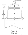
- Figure 1 schematically illustrates a conventional LED having an n-type SiC substrate 10, an active region 12 comprising an n-GaN-based layer 14 and a p-GaN-based layer 16 grown on the substrate and patterned into a mesa.
- a metal p-electrode 18 is deposited on and electrically coupled to the p-GaN layer 16 and a wire bond connection 28 is made to a bond pad 20 on the p-electrode 18.
- An n-eleetrode 22 on and electrically coupled to the conductive substrate is attached to metallic submount 24 using a conductive epoxy 26.
- the conductive epoxy 26 usually silver epoxy
- the LED is pressed into the epoxy 26.
- the epoxy is then heat cured which causes it to harden, providing a stable and electrically conductive mount for the LED chip.
- Light generated in the active region 12 is directed up and out of the device. However, a substantial amount of the generated light may be transmitted into the substrate and partially absorbed by the epoxy 26.
- Flip-chip mounting of LEDs involves mounting the LED onto the submount substrate side up. Light is then extracted and emitted through the transparent substrate.
- Flip chip mounting may be an especially desirable technique for mounting SiC-based LEDs. Since SiC has a higher index of refraction than GaN, light generated in the active region does not internally reflect ( i.e. reflect back into the GaN-based layers) at the GaN/SiC interface.
- Flip chip mounting of SiC-based LEDs may offer improved light extraction when employing certain chip-shaping techniques known in the art.
- Flip chip packaging of SiC LEDs may have other benefits as well, such as improved heat extraction/dissipation, which may be desirable depending on the particular application for the chip.
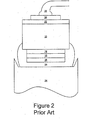
- FIG. 2 One problem with flip-chip mounting is illustrated in Figure 2 . Namely, when a chip is flip-chip mounted on a conductive submount or package conventional techniques may not be possible. Conventionally, a conductive die attach material 26, such as silver epoxy, is deposited on the chip and/or on the submount 24, and the chip is pressed onto the submount 24. This can cause the viscous conductive die attach material 26 to squeeze out and make contact with the n-type layers 14 and 10 in the device, thereby forming a Schottky diode connection that shunts the p-n junction in the active region with predictably undesirable results. Thus, new techniques may be needed for flip-chip mounting of LEDs.
- a conductive die attach material 26 such as silver epoxy
- Embodiments of the present invention provide for mounting a light emitting device having a gallium nitride based light emitting region on a silicon carbide substrate in a flip-chip configuration by mounting an electrode of the gallium nitride based light emitting region to a submount utilizing a B-stage curable die epoxy.
- the electrode is mounted to the submount by forming a predefined pattern of the B-stage curable die epoxy on the electrode, the predefined pattern covering only a predefined portion of the electrode.
- the electrode of the gallium nitride based light emitting region is attached to the submount utilizing the predefined pattern of the B-stage curable die epoxy.
- the predefined pattern of B-stage curable die epoxy may be provided by applying the B-stage curable die epoxy to the electrode by screen printing.
- the screen printing provides a resolution of application of the B-stage curable die epoxy of about 4 mils.
- the predefined pattern of B-stage curable die epoxy may also be provided by dispensing the B-stage epoxy onto desired locations of the electrode. Furthermore, the predefined pattern of B-stage curable die epoxy can be provided by coating the electrode with a B-stage epoxy and selectively removing B-stage epoxy from the electrode to provide the predefined pattern. The B-stage epoxy may be selectively removed by laser scribing the B-stage epoxy to selectively remove epoxy to provide the predefined pattern. If the B-stage epoxy is a photo-sensitive B-stage epoxy the B-stage epoxy may be selectively removed utilizing photolithography to provide the predefined pattern. The predefined pattern of B-stage curable die epoxy may also be provided by pin transferring the B-stage epoxy to locations on the electrode to provide the predefined pattern.
- forming a predefined pattern of B-stage curable die epoxy is followed by pre-curing the B-stage epoxy.
- the pre-curing of the B-stage epoxy can be provided by pre-curing the B-stage epoxy utilizing a temperature of from about 50 to about150 °C.
- the B-stage epoxy can be pre-cured utilizing a temperature of about 85 °C.
- the electrode of the gallium nitride based light emitting region may be attached to the submount utilizing the predefined pattern of the B-stage curable die epoxy by placing the light emitting device on the submount and heating the B-stage epoxy to a final curing temperature so as to cause the B-stage epoxy to re-flow.
- the B-stage epoxy may be heated to a temperature of at least about 150 °C.
- the predefined pattern is a single nodule of B-stage epoxy on the electrode.
- the predefined pattern may also be a plurality of bumps of B-stage epoxy on the electrode.
- the predefined pattern may further be a plurality of lines of B-stage epoxy on the electrode.
- the predefined pattern could also be a criss-cross pattern of B-stage epoxy on the electrode.
- a light emitting device die having a mesa configuration on a substrate and an electrode on the mesa is attached to a submount in a flip-chip configuration by forming predefined pattern of conductive die attach material on at least one of the electrode and the submount and mounting the light emitting device die to the submount.
- the predefined pattern of conductive die attach material is selected so as to prevent the conductive die attach material from contacting sidewalls of the mesa or the substrate when the light emitting device die is mounted to the submount.
- the predefined pattern of conductive die attach material may provide a volume of die attach material that is less than a volume defined by an area of the electrode and a distance between the electrode and the submount.
- the predefined pattern is a single nodule of conductive die attach material on the electrode.
- the predefined pattern may also be a plurality of bumps of conductive die attach material on the electrode.
- the predefined pattern may further be a plurality of lines of conductive die attach material on the electrode.
- the predefined pattern could also be a criss-cross pattern of conductive die attach material on the electrode.
- the conductive die attach material is at least one of a B-stage curable die epoxy, a solder paste, a pattern of solder bumps, and/or a conductive polymer.
- the predefined pattern may be provided by forming a predefined pattern of solder paste by at least one of screen printing, dispensing and/or pin transferring, If the conductive die attach material is solder bumps, the predefined pattern may be provided by forming a predefined pattern of solder bumps by at least one of dispensing a solder paste and reflowing, electroplating and/or dipping.
- the predefined pattern may be provided by forming a pattern of a B-stage curable-die epoxy and/or a conductive polymer by screen printing, dispensing, dispensing and reflowing, layering and laser scribing, photolithography and/or pin transferring methods.
- light emitting device dive suitable for mounting on a submount includes a conducting substrate, such as a silicon carbide substrate, a gallium nitride based active region on the silicon carbide substrate and a first electrode on the gallium nitride based active region opposite the substrate.
- a conducting substrate such as a silicon carbide substrate, a gallium nitride based active region on the silicon carbide substrate and a first electrode on the gallium nitride based active region opposite the substrate.
- the first electrode and the gallium nitride based active region form a mesa having sidewalls.
- a second electrode is provided on the silicon carbide substrate opposite the gallium nitride active region.
- a predefined pattern of conductive die attach material is provided on the first electrode opposite the gallium nitride active region that substantially prevents the conductive die attach material from contacting the sidewalls of the mesa and/or the substrate when the light emitting device die is mounted to the submount.
- the predefined pattern of conductive die attach material may provide a volume of die attach material that is less than a volume defined by an area of the first electrode and a distance between the first electrode and the submount.
- the predefined pattern may be a single nodule of conductive die attach material on the first electrode.
- the predefined pattern may also be a plurality of bumps of conductive die attach material on the first electrode.
- the predefined pattern could be a plurality of lines of conductive die attach material on the first electrode.
- the predefined pattern could also be a criss-cross pattern of conductive die attach material on the first electrode.
- the conductive die attach material may be a B-stage curable die epoxy, a solder paste, a pattern of solder bumps, and/or a conductive polymer.
- a submount may also be provided.
- the first electrode is mounted to the submount by the predefined pattern of conductive die attach material.
- Additional embodiments of the present invention provide a light emitting device die suitable for mounting on a submount that includes a substrate, such as a silicon carbide substrate, a gallium nitride based active region on the substrate and a first electrode on the nitride based active region opposite the substrate.
- the first electrode and the gallium nitride based active region may form a mesa having sidewalls.
- a second electrode may be provided on the substrate opposite the gallium nitride active region.
- the B-stage conductive epoxy is provided on the first electrode opposite the gallium nitride active region
- the B-stage conductive epoxy may be provided in a predefined pattern.
- the predefined pattern of B-stage conductive epoxy may provide a volume of B-stage conductive epoxy that is less than a volume defined by an area of the first electrode and a distance between the first electrode and the submount.
- the predefined pattern may be a single nodule of B-stage conductive epoxy on the first electrode.
- the predefined pattern could also be a plurality of bumps of B-stage conductive epoxy on the first electrode.
- the predefined pattern may further be a plurality of lines of B-stage conductive epoxy on the first electrode.
- the predefined pattern could also be a criss-cross pattern of B-stage conductive epoxy on the first electrode.
- a submount may also be provided.
- the first electrode is mounted to the submount by the B-stage conductive epoxy.
- a light emitting device die includes a gallium nitride based active region having at least one region of a first conductivity type and a first electrode electrically coupled to the gallium nitride based active region.
- a region of semiconductor material of a second conductivity type is electrically coupled to the gallium nitride based active region.
- the second conductivity type is opposite to the first conductivity type.
- a predefined pattern of conductive die attach material is on the first electrode opposite the gallium nitride active region and configured to substantially prevent the conductive die attach material from contacting the region of semiconductor material of a second conductivity type when the light emitting device die is mounted to a submount.
- a second electrode may also be provided on the region of semiconductor material of a second conductivity type.
- a substrate may also be provide and the gallium nitride based active region may be on the substrate.
- the first electrode and the second electrode may be on opposite sides of the substrate or may be on the same side of the substrate.
- the substrate may be insulating or conductive. In certain embodiments of the present invention, the substrate is a silicon carbide substrate.
- Embodiments of the present invention provide for connecting a light emitting device having a light emitting element, such as an LED die, to a submount or package in a flip-chip configuration using a die attach material that can be applied to an electrode of the light emitting device, such as the p-electrode, and/or the submount or package prior to packaging the light emitting device.
- the die attach material can be used to form a conductive attachment between the light emitting device and the submount without forming a parasitic diode that shunts the p-n diode of the device.
- the shunt diode may be avoided by preventing the conductive adhesive from substantially flowing during curing.
- the shunt diode may be avoided by preventing the conductive adhesive from contacting a region of the device of opposite conductivity type to that of the region to which the conductive adhesive provides a contact.
- the shunt diode may be avoided by preventing the conductive adhesive from contacting an n-type region of the device. If the conductive adhesive provides a contact to the n-type contact of the device, the shunt diode may be avoided by preventing the conductive adhesive from contacting a p-type region of the device.
- the conductive adhesive may facilitate heat extraction from the device when the device is mounted in a flip-chip configuration. Such heat extraction may be beneficial for high power devices, such as devices that may be suitable for use in white light applications.
- the present invention is described herein primarily with reference to devices.having contacts on opposite sides of the device, embodiments of the present invention may also be beneficial for devices having both contacts on the same side of the device.
- the conductive adhesive may provided in a manner where the conductive adhesive of the contact do not form a shunt diode by contacting a regions of the device of opposite conductivity type of that to which the conductive adhesive makes contact.
- the conductive adhesive of the two contacts should not contact each other.
- Embodiments of the present invention are described herein with reference to a GaN based LED on an n-type SiC substrate 10 and having a n-type layer 14, a p-type layer 16 and a p-electrode 18 electrically coupled to the p-type layer.
- the present invention should not be construed as limited to such structures.
- references herein to the conductive die attach material shorting to the n-type regions 10 and 14 are provided for illustrative purposes only.
- references to shorting to the n-type regions 10 and 14 may be considered as references to other layers in other device structures (for example to quantum well and/or barrier layers in a multi-quantum well device) where unintentional contact with the die attach material would result in impaired performance, reliability or other characteristics of the device.
- Light emitting devices for use in embodiments of the present invention may be gallium nitride based LEDs or lasers fabricated on a silicon carbide substrate such as those devices manufactured and sold by Cree, Inc. of Durham, North Carolina.
- the present invention may be suitable for use with LEDs and/or lasers as described in United States Patent Nos.
- the light emitting devices may include a p-electrode that provides a reflecting layer to reflect light generated in the active region back through the device.
- Reflective p-electrodes and related structures are described in U.S. Patent Application Serial No. 10/057,82 entitled "LIGHT EMITTING DIODES INCLUDING SUBSTRATE MODIFICATIONS FOR LIGHT EXTRACTION AND MANUFACTURING METHODS THEREFOR” filed January 25, 2002, which is hereby incorporated by reference as if set forth fully herein.
- the LEDs and/or lasers may be configured to operate in a "flip-chip" configuration such that light emission occurs through the substrate.
- the substrate may be patterned so as to enhance light output of the devices as is described, for example, in United States Provisional Patent Application Ser. No. 60/307,235 filed July 23, 2001 entitled “LIGHT EMITTING DIODES INCLUDING SUBSTRATE MODIFICATIONS FOR LIGHT EXTRACTION AND MANUFACTURING METHODS THEREFOR” and United States patent Application Serial No. 10/057,82 filed January 25, 2002 entitled entitled “LIGHT EMITTING DIODES INCLUDING SUBSTRATE MODIFICATIONS FOR LIGHT EXTRACTION AND MANUFACTURING METHODS THEREFOR.”
- the die attach material may be provided in a pattern on the p-electrode of a gallium nitride based light emitting device formed on a silicon carbide substrate.
- the term pattern means that the die attach material covers some, but not all, of the surface on which it is placed.
- the pattern may be selected so as to substantially prevent the conductive die attach material from flowing to the sidewalls of the gallium nitride device so as to short the active region of the device.
- the pattern may be selected to prevent the conductive adhesive from substantially flowing during curing/bonding. Examples of suitable patterns of conducive die attach material are shown in Figures 3A-3D .
- a single nodule of die attach material 30 is provided on a p-electrode 18 of a light emitting device on the substrate 10.
- Figure 3B shows die attach material 30 formed in an array of nodules on the p-electrode 18.
- Figure 3C shows die attach material 30 formed in an array of lines on the p-electrode 18.
- Figure 3D shows die attach material 30 formed in a criss-cross or "X" pattern on the p-electrode 18.
- the pattern of conductive die attach material provides a volume of die attach material which is less than a volume defined by the area of the p-electrode of the light emitting device and the distance between the light emitting device and the submount.
- Suitable die attach materials include a B-stage curable die epoxy (or a "B-stage epoxy"), a solder paste, a pattern of solder bumps, and/or a conductive polymer.
- Embodiments of the invention include methods of applying a die attach material to an LED die or wafer and further include an LED die having deposited thereon a die attach material. Additional embodiments include methods of patterning a die attach material on an LED die or applying a patterned die attach material to an LED die or wafer, and further include the resulting LED die.
- the die attach material may comprise a standard B-stage epoxy.
- epoxies are available commercially from, for example, Emerson Cumming, Ablestik, Dexter, Diemat and Epotek.
- Ablestik's RP333-3 epoxy, Dexter's BMI-519 epoxy and Emerson and Cumming's LA-9843-28 epoxy are suitable B-stage epoxies.
- the epoxy has the following characteristics:
- the B-stage epoxy need not be electrically conductive, and a separate electrically conductive path may be provided.
- the die attach material may comprise a conductive polymer such as CB028 manufactured by DuPont.
- a GaN based light emitting device such as those described above, is fabricated on a SiC substrate (block 100).
- ohmic contacts are formed on opposite sides of the wafer.
- the wafer is patterned into LEDs, for example, by etching to form a plurality of mesas.
- a passivation layer is formed to protect the epitaxial layers such as described in United States Provisional Patent Application Serial No.
- the die attach material may contact the substrate, for example, at a portion where the substrate has been sawn or broken and, thereby form a shunt diode.
- the passivation layer is somehow damaged, for example at a region where the substrate is broken, a contact could unintentionally be made in such areas.
- the die attach material is formed in a predefined pattern on the p-electrode of the LEDs (block 105). If a B-stage epoxy or conductive polymer is used, it may be deposited using any of the following techniques (or a combination of techniques, if desired):
- the B-stage epoxy Once the B-stage epoxy has been deposited, it is pre-cured to cause it to solidify.
- Typical heat ranges for pre-curing are 50-150 °C.
- the pre-curing occurs at temperatures below 85 °C to avoid damaging other materials used in the manufacturing process such as a mounting tape.
- solder paste may be used as the die attach material.
- Solder paste generally includes a solder metal or alloy such as Au/Ge, Pb/Sn, Au/Sn or In mixed together with solvents and/or binders to form a paste.
- Solder paste may be applied by screen printing, dispensing or pin transferring as described above in connection with epoxies.
- pin transferring techniques may be used to provide a solder dot as the pattern of the die attach material. For example, a solder dot of about 0.2 mm formed by pin transfer techniques may be used to attach the device to the submount.
- the die attach material may comprise solder bumps formed on the p-electrode.
- Solder bumps generally includes solder metal without binders or solvents, and may be deposited by, for example, dispensing a solder paste and subsequent reflow, electroplating and/or dipping.
- the wafer is swan and/or sawn and broken using conventional techniques to separate the individual dies (block 110 ). Since the sawing may be done under a flow of de-ionized (DI) water, in some embodiments the conductive die attach material, such as the B-stage epoxy, is able to withstand water as well as the mechanical stress imparted from sawing and breaking. The individual die may then be secured onto adhesive tape rolls to facilitate automated packaging. Additionally, unitized groups of dies may be provided as described in United States Patent Application Serial No. 10/058,369 filed January 28, 2002 , entitled "CLUSTER PACKAGING OF LIGHT EMITTING DIODES,” the disclosure of which is incorporated herein by reference as if set forth fully herein.
- DI de-ionized
- Individual dies may then be attached to a submount utilizing the conductive die attach material on the p-electrode (block 115).
- the die may be set in place on the submount and heated to a final curing temperature (typically in excess of 150 °C). This causes the epoxy to re-flow and create a permanent connection between the LED chip and the submount.
- the conductive die attach material utilized, the pattern of the material on the p-electrode and/or the pressure used during bonding, the conductive material does not flow onto the sidewalls of the mesa and/or the substrate of the device thereby creating a shunt diode in parallel with the active region of the device. A wirebond connection is then made to the n-electrode.
- Figure 4 illustrates embodiments of the present invention where the die attach material is provided on the p-electrode of the device
- the die attach material may be applied directly to the package or submount in a desired pattern or to both the submount and the p-electrode.
- the submount is heated to the final curing temperature and the LED chip is pressed onto the submount. Since a B-stage epoxy is used instead of the less viscous conventional epoxies, there is less likelihood of contacting the n-type layers of the active region of the device with the epoxy.
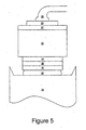
- Figure 5 illustrates an LED mounted in accordance with embodiments of the present invention.
- the die attach material epoxy 30 is disposed between the p-electrode 18 and the submount 24 but does not contact the n-type layer 14 or the substrate 10 of the device.
- the volume of the die attach material 30 is less than the volume defined by the area of the p-electrode 18 and the distance between the p-electrode 18 and the submount 24.
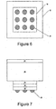
- Figure 6 illustrates a substrate 10 and a p-electrode 18 of a light emitting device on which an array of bumps of conductive die attach material 30 have been formed, such as through deposition, patterning, plating and/or other techniques.
- Figure 7 illustrates the light emitting device of Figure 6 in elevation. After deposition of the bumps 30 the LED is placed on a submount and the device is heated at a temperature sufficient to reflow the bumps 30. In some embodiments, flux may also applied as part of the reflow process. The reflow temperature depends on the particular metal or alloy used.
- alloys containing a high percentage of Sn may have a meting point below 200 °C, while alloys having a low percentage of Sn may have a melting point above 350 °C.
- surface tension keeps the bumps from outflowing and wetting the n-type layer 14 or the substrate 10 of the LED.
- non-wettable patterns and/or solder dams may be used to control outflow.
- FIG 8 illustrates an LED mounted in accordance with these embodiments of the present invention.
- the bumps of die attach material epoxy 30 are disposed between the p-electrode 18 and the submount 24 but do not contact the n-type layer 14 or the substrate 10 of the device.
- the volume of the die attach material 30 e.g . the solder bumps
- the volume of the die attach material 30 is less than the volume defined by the area of the p-electrode 18 and the distance between the p-electrode 18 and the submount 24. Therefore, no Schottky diode connection is made between the solder bumps and the n-type portions of the LED.
Landscapes
- Led Device Packages (AREA)
- Wire Bonding (AREA)
Applications Claiming Priority (3)
| Application Number | Priority Date | Filing Date | Title |
|---|---|---|---|
| US30731101P | 2001-07-23 | 2001-07-23 | |
| US10/185,252 US6888167B2 (en) | 2001-07-23 | 2002-06-27 | Flip-chip bonding of light emitting devices and light emitting devices suitable for flip-chip bonding |
| EP02752483A EP1417722B1 (de) | 2001-07-23 | 2002-07-22 | Flip-chip bonden von licht-emittierenden chips |
Related Parent Applications (2)
| Application Number | Title | Priority Date | Filing Date |
|---|---|---|---|
| EP02752483.4 Division | 2002-07-22 | ||
| EP02752483A Division EP1417722B1 (de) | 2001-07-23 | 2002-07-22 | Flip-chip bonden von licht-emittierenden chips |
Publications (2)
| Publication Number | Publication Date |
|---|---|
| EP2262017A2 true EP2262017A2 (de) | 2010-12-15 |
| EP2262017A3 EP2262017A3 (de) | 2017-01-04 |
Family
ID=26880972
Family Applications (2)
| Application Number | Title | Priority Date | Filing Date |
|---|---|---|---|
| EP02752483A Expired - Lifetime EP1417722B1 (de) | 2001-07-23 | 2002-07-22 | Flip-chip bonden von licht-emittierenden chips |
| EP10179427.9A Withdrawn EP2262017A3 (de) | 2001-07-23 | 2002-07-22 | Flip-Chip-Kleben von lichtemittierenden Vorrichtungen und zum Flip-Chip-Kleben geeignete lichtemittierende Vorrichtungen |
Family Applications Before (1)
| Application Number | Title | Priority Date | Filing Date |
|---|---|---|---|
| EP02752483A Expired - Lifetime EP1417722B1 (de) | 2001-07-23 | 2002-07-22 | Flip-chip bonden von licht-emittierenden chips |
Country Status (9)
| Country | Link |
|---|---|
| US (3) | US6888167B2 (de) |
| EP (2) | EP1417722B1 (de) |
| JP (1) | JP2005510043A (de) |
| KR (1) | KR20040029381A (de) |
| CN (1) | CN100392874C (de) |
| AT (1) | ATE527698T1 (de) |
| CA (1) | CA2454797A1 (de) |
| TW (1) | TW578276B (de) |
| WO (1) | WO2003010833A2 (de) |
Families Citing this family (78)
| Publication number | Priority date | Publication date | Assignee | Title |
|---|---|---|---|---|
| US6747298B2 (en) * | 2001-07-23 | 2004-06-08 | Cree, Inc. | Collets for bonding of light emitting diodes having shaped substrates |
| AU2003263779A1 (en) | 2002-07-22 | 2004-02-09 | Cree, Inc. | Light emitting diode including barrier layers and manufacturing methods therefor |
| US7009199B2 (en) * | 2002-10-22 | 2006-03-07 | Cree, Inc. | Electronic devices having a header and antiparallel connected light emitting diodes for producing light from AC current |
| KR101020387B1 (ko) * | 2002-12-20 | 2011-03-08 | 크리 인코포레이티드 | 반도체 메사 구조와 도전형 접합을 포함하는 전자 소자 및그 제조방법 |
| US20040188696A1 (en) * | 2003-03-28 | 2004-09-30 | Gelcore, Llc | LED power package |
| DE10314876B4 (de) * | 2003-04-01 | 2008-02-14 | Infineon Technologies Ag | Verfahren zum mehrstufigen Herstellen von Diffusionslötverbindungen und seine Verwendung für Leistungsbauteile mit Halbleiterchips |
| JP4766845B2 (ja) * | 2003-07-25 | 2011-09-07 | シャープ株式会社 | 窒化物系化合物半導体発光素子およびその製造方法 |
| JP2005203519A (ja) * | 2004-01-14 | 2005-07-28 | Sumitomo Electric Ind Ltd | 半導体発光装置 |
| TWI230425B (en) | 2004-02-06 | 2005-04-01 | South Epitaxy Corp | Bumping process for light emitting diode |
| CN100347867C (zh) * | 2004-02-26 | 2007-11-07 | 元砷光电科技股份有限公司 | 发光二极管的焊球制造工艺 |
| US7419912B2 (en) * | 2004-04-01 | 2008-09-02 | Cree, Inc. | Laser patterning of light emitting devices |
| US7462861B2 (en) * | 2004-04-28 | 2008-12-09 | Cree, Inc. | LED bonding structures and methods of fabricating LED bonding structures |
| WO2006005062A2 (en) * | 2004-06-30 | 2006-01-12 | Cree, Inc. | Chip-scale methods for packaging light emitting devices and chip-scale packaged light emitting devices |
| JP4644193B2 (ja) * | 2004-07-12 | 2011-03-02 | ローム株式会社 | 半導体発光素子 |
| US7405093B2 (en) * | 2004-08-18 | 2008-07-29 | Cree, Inc. | Methods of assembly for a semiconductor light emitting device package |
| US8513686B2 (en) * | 2004-09-22 | 2013-08-20 | Cree, Inc. | High output small area group III nitride LEDs |
| US7737459B2 (en) * | 2004-09-22 | 2010-06-15 | Cree, Inc. | High output group III nitride light emitting diodes |
| US8174037B2 (en) | 2004-09-22 | 2012-05-08 | Cree, Inc. | High efficiency group III nitride LED with lenticular surface |
| US7259402B2 (en) * | 2004-09-22 | 2007-08-21 | Cree, Inc. | High efficiency group III nitride-silicon carbide light emitting diode |
| US8288942B2 (en) * | 2004-12-28 | 2012-10-16 | Cree, Inc. | High efficacy white LED |
| TWI422044B (zh) * | 2005-06-30 | 2014-01-01 | 克立公司 | 封裝發光裝置之晶片尺度方法及經晶片尺度封裝之發光裝置 |
| US20070015300A1 (en) * | 2005-07-15 | 2007-01-18 | Yu-Chuan Liu | Method for fabricating a light-emitting device |
| US20070063344A1 (en) * | 2005-09-22 | 2007-03-22 | Chun-Hung Lin | Chip package structure and bumping process |
| WO2007081719A2 (en) | 2006-01-05 | 2007-07-19 | Illumitex, Inc. | Separate optical device for directing light from an led |
| US8596819B2 (en) * | 2006-05-31 | 2013-12-03 | Cree, Inc. | Lighting device and method of lighting |
| DE102006033873A1 (de) * | 2006-07-21 | 2008-01-24 | Patent-Treuhand-Gesellschaft für elektrische Glühlampen mbH | Strahlungsemittierende Einrichtung mit mehreren strahlungs-emittierenden Bauelementen und Beleuchtungseinrichtung |
| US7635869B2 (en) | 2006-09-14 | 2009-12-22 | Lumination Llc | Support with recessed electrically conductive chip attachment material for flip-chip bonding a light emitting chip |
| US8087960B2 (en) | 2006-10-02 | 2012-01-03 | Illumitex, Inc. | LED system and method |
| US10873002B2 (en) * | 2006-10-20 | 2020-12-22 | Cree, Inc. | Permanent wafer bonding using metal alloy preform discs |
| US20080121911A1 (en) * | 2006-11-28 | 2008-05-29 | Cree, Inc. | Optical preforms for solid state light emitting dice, and methods and systems for fabricating and assembling same |
| CN102683376A (zh) | 2007-01-22 | 2012-09-19 | 科锐公司 | 高压发光体、发光体及照明装置 |
| US9391118B2 (en) * | 2007-01-22 | 2016-07-12 | Cree, Inc. | Fault tolerant light emitters, systems incorporating fault tolerant light emitters and methods of fabricating fault tolerant light emitters |
| US20080283864A1 (en) * | 2007-05-16 | 2008-11-20 | Letoquin Ronan P | Single Crystal Phosphor Light Conversion Structures for Light Emitting Devices |
| JP4987632B2 (ja) * | 2007-08-30 | 2012-07-25 | 株式会社東芝 | 半導体素子の製造方法、サブマウントの製造方法及び電子部品 |
| US8008707B2 (en) * | 2007-12-14 | 2011-08-30 | Kabushiki Kaisha Toshiba | Nonvolatile semiconductor memory device provided with charge storage layer in memory cell |
| JP2011512037A (ja) | 2008-02-08 | 2011-04-14 | イルミテックス, インコーポレイテッド | エミッタ層成形のためのシステムおよび方法 |
| US7791101B2 (en) * | 2008-03-28 | 2010-09-07 | Cree, Inc. | Indium gallium nitride-based ohmic contact layers for gallium nitride-based devices |
| US9147812B2 (en) * | 2008-06-24 | 2015-09-29 | Cree, Inc. | Methods of assembly for a semiconductor light emitting device package |
| TW201034256A (en) | 2008-12-11 | 2010-09-16 | Illumitex Inc | Systems and methods for packaging light-emitting diode devices |
| US20100248424A1 (en) * | 2009-03-27 | 2010-09-30 | Intellectual Business Machines Corporation | Self-Aligned Chip Stacking |
| US9437785B2 (en) * | 2009-08-10 | 2016-09-06 | Cree, Inc. | Light emitting diodes including integrated backside reflector and die attach |
| US8449128B2 (en) | 2009-08-20 | 2013-05-28 | Illumitex, Inc. | System and method for a lens and phosphor layer |
| US8585253B2 (en) | 2009-08-20 | 2013-11-19 | Illumitex, Inc. | System and method for color mixing lens array |
| DE102010009717A1 (de) | 2010-03-01 | 2011-09-01 | Osram Opto Semiconductors Gmbh | Leuchtdiodenchip |
| US9991427B2 (en) * | 2010-03-08 | 2018-06-05 | Cree, Inc. | Photonic crystal phosphor light conversion structures for light emitting devices |
| US8519298B2 (en) * | 2010-03-25 | 2013-08-27 | Veeco Instruments, Inc. | Split laser scribe |
| TWI407536B (zh) * | 2010-12-10 | 2013-09-01 | 國立成功大學 | 半導體元件之散熱座的製作方法 |
| TW201230910A (en) * | 2011-01-11 | 2012-07-16 | Hon Hai Prec Ind Co Ltd | The method of manufacturing the LED lightbar and the equipment thereof |
| DE102011112000B4 (de) | 2011-08-31 | 2023-11-30 | OSRAM Opto Semiconductors Gesellschaft mit beschränkter Haftung | Leuchtdiodenchip |
| US8426255B2 (en) * | 2011-09-14 | 2013-04-23 | Chipmos Technologies, Inc. | Chip package structure and method for manufacturing the same |
| US11160148B2 (en) | 2017-06-13 | 2021-10-26 | Ideal Industries Lighting Llc | Adaptive area lamp |
| US11792898B2 (en) | 2012-07-01 | 2023-10-17 | Ideal Industries Lighting Llc | Enhanced fixtures for area lighting |
| US8933433B2 (en) | 2012-07-30 | 2015-01-13 | LuxVue Technology Corporation | Method and structure for receiving a micro device |
| US9484504B2 (en) | 2013-05-14 | 2016-11-01 | Apple Inc. | Micro LED with wavelength conversion layer |
| US9111464B2 (en) | 2013-06-18 | 2015-08-18 | LuxVue Technology Corporation | LED display with wavelength conversion layer |
| US9671362B2 (en) * | 2013-07-29 | 2017-06-06 | Honeywell International Inc. | ph sensor with bonding agent disposed in a pattern |
| US9664641B2 (en) | 2013-07-29 | 2017-05-30 | Honeywell International Inc. | pH sensor with substrate or bonding layer configured to maintain piezoresistance of the ISFET die |
| US9972557B2 (en) * | 2014-12-11 | 2018-05-15 | Stmicroelectronics Pte Ltd | Integrated circuit (IC) package with a solder receiving area and associated methods |
| DE102015002176A1 (de) * | 2015-02-24 | 2016-08-25 | Jenoptik Laser Gmbh | Verfahren zum Herstellen eines Diodenlasers und Diodenlaser |
| EP3357097B1 (de) | 2015-10-01 | 2020-12-16 | Cree, Inc. | Flip-chip-festkörperbeleuchtungsvorrichtung mit geringem optischen verlust |
| US10529696B2 (en) | 2016-04-12 | 2020-01-07 | Cree, Inc. | High density pixelated LED and devices and methods thereof |
| CN105921356B (zh) * | 2016-05-20 | 2018-06-26 | 中国电子科技集团公司第十研究所 | 全自动芯片贴装回形蘸胶头 |
| CN105903639B (zh) * | 2016-05-20 | 2018-06-26 | 中国电子科技集团公司第十研究所 | 全自动芯片贴装x形点蘸胶头 |
| KR20170139924A (ko) | 2016-06-10 | 2017-12-20 | 엘지전자 주식회사 | 투명 발광다이오드 필름 |
| US10312415B2 (en) | 2017-06-19 | 2019-06-04 | Microsoft Technology Licensing, Llc | Flexible electronic assembly with semiconductor die |
| US10734363B2 (en) | 2017-08-03 | 2020-08-04 | Cree, Inc. | High density pixelated-LED chips and chip array devices |
| WO2019028314A1 (en) | 2017-08-03 | 2019-02-07 | Cree, Inc. | HIGH DENSITY PIXELIZED LED CHIPS AND NETWORK DEVICES AND METHODS OF MANUFACTURE |
| US11031527B2 (en) | 2018-01-29 | 2021-06-08 | Creeled, Inc. | Reflective layers for light-emitting diodes |
| US11387389B2 (en) | 2018-01-29 | 2022-07-12 | Creeled, Inc. | Reflective layers for light-emitting diodes |
| US11923481B2 (en) | 2018-01-29 | 2024-03-05 | Creeled, Inc. | Reflective layers for light-emitting diodes |
| US10529773B2 (en) | 2018-02-14 | 2020-01-07 | Cree, Inc. | Solid state lighting devices with opposing emission directions |
| CN109346405B (zh) * | 2018-11-23 | 2021-12-03 | 江苏新广联科技股份有限公司 | 一种GaN基SBD倒装芯片的制备方法 |
| US10879441B2 (en) | 2018-12-17 | 2020-12-29 | Cree, Inc. | Interconnects for light emitting diode chips |
| US10903265B2 (en) | 2018-12-21 | 2021-01-26 | Cree, Inc. | Pixelated-LED chips and chip array devices, and fabrication methods |
| US10985294B2 (en) | 2019-03-19 | 2021-04-20 | Creeled, Inc. | Contact structures for light emitting diode chips |
| US11094848B2 (en) | 2019-08-16 | 2021-08-17 | Creeled, Inc. | Light-emitting diode chip structures |
| WO2021087109A1 (en) | 2019-10-29 | 2021-05-06 | Cree, Inc. | Texturing for high density pixelated-led chips |
| US11437548B2 (en) | 2020-10-23 | 2022-09-06 | Creeled, Inc. | Pixelated-LED chips with inter-pixel underfill materials, and fabrication methods |
Citations (14)
| Publication number | Priority date | Publication date | Assignee | Title |
|---|---|---|---|---|
| US4918497A (en) | 1988-12-14 | 1990-04-17 | Cree Research, Inc. | Blue light emitting diode formed in silicon carbide |
| US4966862A (en) | 1989-08-28 | 1990-10-30 | Cree Research, Inc. | Method of production of light emitting diodes |
| US5027168A (en) | 1988-12-14 | 1991-06-25 | Cree Research, Inc. | Blue light emitting diode formed in silicon carbide |
| US5210051A (en) | 1990-03-27 | 1993-05-11 | Cree Research, Inc. | High efficiency light emitting diodes from bipolar gallium nitride |
| US5338944A (en) | 1993-09-22 | 1994-08-16 | Cree Research, Inc. | Blue light-emitting diode with degenerate junction structure |
| US5393993A (en) | 1993-12-13 | 1995-02-28 | Cree Research, Inc. | Buffer structure between silicon carbide and gallium nitride and resulting semiconductor devices |
| US5416342A (en) | 1993-06-23 | 1995-05-16 | Cree Research, Inc. | Blue light-emitting diode with high external quantum efficiency |
| US5523589A (en) | 1994-09-20 | 1996-06-04 | Cree Research, Inc. | Vertical geometry light emitting diode with group III nitride active layer and extended lifetime |
| US5604135A (en) | 1994-08-12 | 1997-02-18 | Cree Research, Inc. | Method of forming green light emitting diode in silicon carbide |
| US5631190A (en) | 1994-10-07 | 1997-05-20 | Cree Research, Inc. | Method for producing high efficiency light-emitting diodes and resulting diode structures |
| US5739554A (en) | 1995-05-08 | 1998-04-14 | Cree Research, Inc. | Double heterojunction light emitting diode with gallium nitride active layer |
| US5782102A (en) | 1992-04-24 | 1998-07-21 | Nippondenso Co., Ltd. | Automotive air conditioner having condenser and evaporator provided within air duct |
| US5836902A (en) | 1996-12-03 | 1998-11-17 | Gray; James C. | Splint |
| US6187606B1 (en) | 1997-10-07 | 2001-02-13 | Cree, Inc. | Group III nitride photonic devices on silicon carbide substrates with conductive buffer interlayer structure |
Family Cites Families (55)
| Publication number | Priority date | Publication date | Assignee | Title |
|---|---|---|---|---|
| JPS559442B2 (de) | 1972-02-24 | 1980-03-10 | ||
| JPS559442A (en) | 1978-07-05 | 1980-01-23 | Matsushita Electric Ind Co Ltd | Light emission element and its manufacturing method |
| JPS55148477A (en) | 1979-05-08 | 1980-11-19 | Sanyo Electric Co Ltd | Fabricating method of light emitting diode |
| JPS5664484A (en) | 1979-10-30 | 1981-06-01 | Toshiba Corp | Led device |
| JPS57153479A (en) * | 1981-03-17 | 1982-09-22 | Matsushita Electric Ind Co Ltd | Nitride gallium light emitting element |
| FR2610451B1 (fr) | 1987-01-30 | 1989-04-21 | Radiotechnique Compelec | Dispositif opto-electronique comprenant au moins un composant monte sur un support |
| JPH01214141A (ja) * | 1988-02-23 | 1989-08-28 | Nec Corp | フリップチップ型半導体装置 |
| GB2249428A (en) * | 1988-08-11 | 1992-05-06 | Plessey Co Plc | Connections for led arrays |
| JP2722601B2 (ja) | 1989-02-06 | 1998-03-04 | 松下電器産業株式会社 | ダイボンディング装置及びダイボンディング方法 |
| EP0397911A1 (de) * | 1989-05-19 | 1990-11-22 | Siemens Aktiengesellschaft | Optoelektronisches Halbleiterbauelement |
| US5068708A (en) * | 1989-10-02 | 1991-11-26 | Advanced Micro Devices, Inc. | Ground plane for plastic encapsulated integrated circuit die packages |
| US5117279A (en) | 1990-03-23 | 1992-05-26 | Motorola, Inc. | Semiconductor device having a low temperature uv-cured epoxy seal |
| US5118584A (en) * | 1990-06-01 | 1992-06-02 | Eastman Kodak Company | Method of producing microbump circuits for flip chip mounting |
| JPH04152645A (ja) | 1990-10-17 | 1992-05-26 | Toshiba Corp | ダイボンディング用コレット |
| JPH0529364A (ja) | 1991-07-17 | 1993-02-05 | Sharp Corp | 半導体素子のボンデイング方法及び装置 |
| US5265792A (en) | 1992-08-20 | 1993-11-30 | Hewlett-Packard Company | Light source and technique for mounting light emitting diodes |
| TW253997B (de) | 1992-09-25 | 1995-08-11 | Philips Electronics Nv | |
| US5438477A (en) * | 1993-08-12 | 1995-08-01 | Lsi Logic Corporation | Die-attach technique for flip-chip style mounting of semiconductor dies |
| JP3054021B2 (ja) * | 1993-12-27 | 2000-06-19 | 株式会社東芝 | 化合物半導体装置 |
| JPH07302858A (ja) | 1994-04-28 | 1995-11-14 | Toshiba Corp | 半導体パッケージ |
| JP2540787B2 (ja) | 1994-07-22 | 1996-10-09 | 日本電気株式会社 | 半導体装置の製造方法 |
| US5539153A (en) * | 1994-08-08 | 1996-07-23 | Hewlett-Packard Company | Method of bumping substrates by contained paste deposition |
| US5694482A (en) | 1994-11-08 | 1997-12-02 | Universal Instruments Corporation | System and method for locating solder bumps on semiconductor chips or chip carriers |
| JP3195720B2 (ja) | 1994-12-20 | 2001-08-06 | シャープ株式会社 | 多色led素子およびその多色led素子を用いたled表示装置、並びに多色led素子の製造方法 |
| KR100367702B1 (ko) * | 1995-03-20 | 2003-04-07 | 유나이티브 인터내셔널 리미티드 | 티타늄장벽층을포함하는솔더범프제조방법및구조 |
| JP2625654B2 (ja) * | 1995-04-28 | 1997-07-02 | 日本電気株式会社 | 半導体装置およびその製造方法 |
| DE19548046C2 (de) * | 1995-12-21 | 1998-01-15 | Siemens Matsushita Components | Verfahren zur Herstellung von für eine Flip-Chip-Montage geeigneten Kontakten von elektrischen Bauelementen |
| US6224690B1 (en) * | 1995-12-22 | 2001-05-01 | International Business Machines Corporation | Flip-Chip interconnections using lead-free solders |
| US5760479A (en) | 1996-02-29 | 1998-06-02 | Texas Instruments Incorporated | Flip-chip die attachment for a high temperature die to substrate bond |
| EP1959506A2 (de) * | 1997-01-31 | 2008-08-20 | Matsushita Electric Industrial Co., Ltd. | Herstellungsverfahren für eine lichtemittierende Halbleitervorrichtung |
| JPH10256313A (ja) | 1997-03-12 | 1998-09-25 | Dekusutaa Kk | 電子素子チップと実装基板の電気的接合方法 |
| JPH11354848A (ja) * | 1998-06-10 | 1999-12-24 | Matsushita Electron Corp | 半導体発光装置 |
| US6189772B1 (en) * | 1998-08-31 | 2001-02-20 | Micron Technology, Inc. | Method of forming a solder ball |
| US6189208B1 (en) * | 1998-09-11 | 2001-02-20 | Polymer Flip Chip Corp. | Flip chip mounting technique |
| JP2000123957A (ja) | 1998-10-14 | 2000-04-28 | Co-Op Chem Co Ltd | 面状発熱体の電極部 |
| US6168972B1 (en) * | 1998-12-22 | 2001-01-02 | Fujitsu Limited | Flip chip pre-assembly underfill process |
| JP2000208822A (ja) | 1999-01-11 | 2000-07-28 | Matsushita Electronics Industry Corp | 半導体発光装置 |
| US6146984A (en) * | 1999-10-08 | 2000-11-14 | Agilent Technologies Inc. | Method and structure for uniform height solder bumps on a semiconductor wafer |
| US6214733B1 (en) * | 1999-11-17 | 2001-04-10 | Elo Technologies, Inc. | Process for lift off and handling of thin film materials |
| US6614056B1 (en) * | 1999-12-01 | 2003-09-02 | Cree Lighting Company | Scalable led with improved current spreading structures |
| HK1048709A1 (zh) * | 1999-12-03 | 2003-04-11 | Cree, Inc. | 透过使用内置及外置光元件提高发光二极管(led)中的抽光效果 |
| JP4897133B2 (ja) | 1999-12-09 | 2012-03-14 | ソニー株式会社 | 半導体発光素子、その製造方法および配設基板 |
| US6213789B1 (en) | 1999-12-15 | 2001-04-10 | Xerox Corporation | Method and apparatus for interconnecting devices using an adhesive |
| US6486499B1 (en) * | 1999-12-22 | 2002-11-26 | Lumileds Lighting U.S., Llc | III-nitride light-emitting device with increased light generating capability |
| US6514782B1 (en) | 1999-12-22 | 2003-02-04 | Lumileds Lighting, U.S., Llc | Method of making a III-nitride light-emitting device with increased light generating capability |
| US6885035B2 (en) | 1999-12-22 | 2005-04-26 | Lumileds Lighting U.S., Llc | Multi-chip semiconductor LED assembly |
| US20020068373A1 (en) * | 2000-02-16 | 2002-06-06 | Nova Crystals, Inc. | Method for fabricating light emitting diodes |
| DE20024002U1 (de) | 2000-03-17 | 2009-03-26 | Tridonicatco Gmbh & Co. Kg | Spannungsversorgung von Leuchtdioden (LEDs) |
| CN1252837C (zh) * | 2000-04-26 | 2006-04-19 | 奥斯兰姆奥普托半导体股份有限两合公司 | 在GaN基板上的发光二极管芯片和用GaN基板上的发光二极管芯片制造发光二极管元件的方法 |
| US6400033B1 (en) * | 2000-06-01 | 2002-06-04 | Amkor Technology, Inc. | Reinforcing solder connections of electronic devices |
| US6506681B2 (en) * | 2000-12-06 | 2003-01-14 | Micron Technology, Inc. | Thin flip—chip method |
| US20020076854A1 (en) * | 2000-12-15 | 2002-06-20 | Pierce John L. | System, method and apparatus for constructing a semiconductor wafer-interposer using B-Stage laminates |
| US6547249B2 (en) | 2001-03-29 | 2003-04-15 | Lumileds Lighting U.S., Llc | Monolithic series/parallel led arrays formed on highly resistive substrates |
| US6455878B1 (en) * | 2001-05-15 | 2002-09-24 | Lumileds Lighting U.S., Llc | Semiconductor LED flip-chip having low refractive index underfill |
| US6498355B1 (en) | 2001-10-09 | 2002-12-24 | Lumileds Lighting, U.S., Llc | High flux LED array |
-
2002
- 2002-06-27 US US10/185,252 patent/US6888167B2/en not_active Expired - Lifetime
- 2002-07-22 WO PCT/US2002/023120 patent/WO2003010833A2/en not_active Ceased
- 2002-07-22 JP JP2003516109A patent/JP2005510043A/ja active Pending
- 2002-07-22 CN CNB028186206A patent/CN100392874C/zh not_active Expired - Lifetime
- 2002-07-22 AT AT02752483T patent/ATE527698T1/de not_active IP Right Cessation
- 2002-07-22 TW TW091116245A patent/TW578276B/zh not_active IP Right Cessation
- 2002-07-22 EP EP02752483A patent/EP1417722B1/de not_active Expired - Lifetime
- 2002-07-22 KR KR10-2004-7001063A patent/KR20040029381A/ko not_active Withdrawn
- 2002-07-22 EP EP10179427.9A patent/EP2262017A3/de not_active Withdrawn
- 2002-07-22 CA CA002454797A patent/CA2454797A1/en not_active Abandoned
-
2004
- 2004-08-17 US US10/920,101 patent/US7259033B2/en not_active Expired - Lifetime
-
2007
- 2007-07-02 US US11/772,419 patent/US7608860B2/en not_active Expired - Lifetime
Patent Citations (17)
| Publication number | Priority date | Publication date | Assignee | Title |
|---|---|---|---|---|
| US4918497A (en) | 1988-12-14 | 1990-04-17 | Cree Research, Inc. | Blue light emitting diode formed in silicon carbide |
| US5027168A (en) | 1988-12-14 | 1991-06-25 | Cree Research, Inc. | Blue light emitting diode formed in silicon carbide |
| US4966862A (en) | 1989-08-28 | 1990-10-30 | Cree Research, Inc. | Method of production of light emitting diodes |
| US5210051A (en) | 1990-03-27 | 1993-05-11 | Cree Research, Inc. | High efficiency light emitting diodes from bipolar gallium nitride |
| US5782102A (en) | 1992-04-24 | 1998-07-21 | Nippondenso Co., Ltd. | Automotive air conditioner having condenser and evaporator provided within air duct |
| US5416342A (en) | 1993-06-23 | 1995-05-16 | Cree Research, Inc. | Blue light-emitting diode with high external quantum efficiency |
| US5338944A (en) | 1993-09-22 | 1994-08-16 | Cree Research, Inc. | Blue light-emitting diode with degenerate junction structure |
| US5393993A (en) | 1993-12-13 | 1995-02-28 | Cree Research, Inc. | Buffer structure between silicon carbide and gallium nitride and resulting semiconductor devices |
| US5604135A (en) | 1994-08-12 | 1997-02-18 | Cree Research, Inc. | Method of forming green light emitting diode in silicon carbide |
| US5523589A (en) | 1994-09-20 | 1996-06-04 | Cree Research, Inc. | Vertical geometry light emitting diode with group III nitride active layer and extended lifetime |
| US5631190A (en) | 1994-10-07 | 1997-05-20 | Cree Research, Inc. | Method for producing high efficiency light-emitting diodes and resulting diode structures |
| US5912477A (en) | 1994-10-07 | 1999-06-15 | Cree Research, Inc. | High efficiency light emitting diodes |
| US5739554A (en) | 1995-05-08 | 1998-04-14 | Cree Research, Inc. | Double heterojunction light emitting diode with gallium nitride active layer |
| US6120600A (en) | 1995-05-08 | 2000-09-19 | Cree, Inc. | Double heterojunction light emitting diode with gallium nitride active layer |
| US5836902A (en) | 1996-12-03 | 1998-11-17 | Gray; James C. | Splint |
| US6187606B1 (en) | 1997-10-07 | 2001-02-13 | Cree, Inc. | Group III nitride photonic devices on silicon carbide substrates with conductive buffer interlayer structure |
| US6201262B1 (en) | 1997-10-07 | 2001-03-13 | Cree, Inc. | Group III nitride photonic devices on silicon carbide substrates with conductive buffer interlay structure |
Also Published As
| Publication number | Publication date |
|---|---|
| CA2454797A1 (en) | 2003-02-06 |
| WO2003010833A2 (en) | 2003-02-06 |
| EP1417722B1 (de) | 2011-10-05 |
| ATE527698T1 (de) | 2011-10-15 |
| TW578276B (en) | 2004-03-01 |
| WO2003010833A3 (en) | 2004-03-11 |
| KR20040029381A (ko) | 2004-04-06 |
| US20050017256A1 (en) | 2005-01-27 |
| CN100392874C (zh) | 2008-06-04 |
| US7259033B2 (en) | 2007-08-21 |
| CN1557025A (zh) | 2004-12-22 |
| US20070241360A1 (en) | 2007-10-18 |
| EP1417722A2 (de) | 2004-05-12 |
| US7608860B2 (en) | 2009-10-27 |
| US6888167B2 (en) | 2005-05-03 |
| EP2262017A3 (de) | 2017-01-04 |
| JP2005510043A (ja) | 2005-04-14 |
| US20030045015A1 (en) | 2003-03-06 |
Similar Documents
| Publication | Publication Date | Title |
|---|---|---|
| US6888167B2 (en) | Flip-chip bonding of light emitting devices and light emitting devices suitable for flip-chip bonding | |
| US7642121B2 (en) | LED bonding structures and methods of fabricating LED bonding structures | |
| EP1653523B1 (de) | Leuchtdioden-Verpackung | |
| EP1774598B1 (de) | Verfahren zum kapseln eines lichtemittierenden bauelements und gekapselte lichtemittierende bauelemente im chip-massstab | |
| US7405093B2 (en) | Methods of assembly for a semiconductor light emitting device package | |
| US7977686B2 (en) | Chip-scale methods for packaging light emitting devices and chip-scale packaged light emitting devices | |
| KR20120109497A (ko) | 플립 칩 led를 위한 실리콘 기반 반사성 언더필 및 열 커플러 | |
| WO2024030891A1 (en) | Wafer level fabrication for multiple chip light-emitting devices |
Legal Events
| Date | Code | Title | Description |
|---|---|---|---|
| PUAI | Public reference made under article 153(3) epc to a published international application that has entered the european phase |
Free format text: ORIGINAL CODE: 0009012 |
|
| AC | Divisional application: reference to earlier application |
Ref document number: 1417722 Country of ref document: EP Kind code of ref document: P |
|
| AK | Designated contracting states |
Kind code of ref document: A2 Designated state(s): AT BE BG CH CY CZ DE DK EE ES FI FR GB GR IE IT LI LU MC NL PT SE SK TR |
|
| RIN1 | Information on inventor provided before grant (corrected) |
Inventor name: MOHAMMED, ANWAR Inventor name: BHARATHAN, JAYESH Inventor name: ANDREWS, PETER Inventor name: EDMOND, JOHN Inventor name: SLATER, DAVID Inventor name: NEGLEY, GERALD H. Inventor name: RAFFETTO, MARK |
|
| PUAL | Search report despatched |
Free format text: ORIGINAL CODE: 0009013 |
|
| AK | Designated contracting states |
Kind code of ref document: A3 Designated state(s): AT BE BG CH CY CZ DE DK EE ES FI FR GB GR IE IT LI LU MC NL PT SE SK TR |
|
| RIC1 | Information provided on ipc code assigned before grant |
Ipc: H01L 33/62 20100101AFI20161201BHEP |
|
| STAA | Information on the status of an ep patent application or granted ep patent |
Free format text: STATUS: THE APPLICATION IS DEEMED TO BE WITHDRAWN |
|
| 18D | Application deemed to be withdrawn |
Effective date: 20170705 |