EP2267543A2 - Elektrofotografischer Fotorezeptor, Bilderzeugungsvorrichtung und Prozesskartusche - Google Patents
Elektrofotografischer Fotorezeptor, Bilderzeugungsvorrichtung und Prozesskartusche Download PDFInfo
- Publication number
- EP2267543A2 EP2267543A2 EP10156225A EP10156225A EP2267543A2 EP 2267543 A2 EP2267543 A2 EP 2267543A2 EP 10156225 A EP10156225 A EP 10156225A EP 10156225 A EP10156225 A EP 10156225A EP 2267543 A2 EP2267543 A2 EP 2267543A2
- Authority
- EP
- European Patent Office
- Prior art keywords
- charge transporting
- electrophotographic photoreceptor
- transporting materials
- surface layer
- weight
- Prior art date
- Legal status (The legal status is an assumption and is not a legal conclusion. Google has not performed a legal analysis and makes no representation as to the accuracy of the status listed.)
- Withdrawn
Links
Images


Classifications
-
- G—PHYSICS
- G03—PHOTOGRAPHY; CINEMATOGRAPHY; ANALOGOUS TECHNIQUES USING WAVES OTHER THAN OPTICAL WAVES; ELECTROGRAPHY; HOLOGRAPHY
- G03G—ELECTROGRAPHY; ELECTROPHOTOGRAPHY; MAGNETOGRAPHY
- G03G5/00—Recording-members for original recording by exposure, e.g. to light, to heat or to electrons; Manufacture thereof; Selection of materials therefor
- G03G5/14—Inert intermediate or cover layers for charge-receiving layers
- G03G5/142—Inert intermediate layers
- G03G5/144—Inert intermediate layers comprising inorganic material
-
- G—PHYSICS
- G03—PHOTOGRAPHY; CINEMATOGRAPHY; ANALOGOUS TECHNIQUES USING WAVES OTHER THAN OPTICAL WAVES; ELECTROGRAPHY; HOLOGRAPHY
- G03G—ELECTROGRAPHY; ELECTROPHOTOGRAPHY; MAGNETOGRAPHY
- G03G5/00—Recording-members for original recording by exposure, e.g. to light, to heat or to electrons; Manufacture thereof; Selection of materials therefor
- G03G5/02—Charge-receiving layers
- G03G5/04—Photoconductive layers; Charge-generation layers or charge-transporting layers; Additives therefor; Binders therefor
- G03G5/05—Organic bonding materials; Methods for coating a substrate with a photoconductive layer; Inert supplements for use in photoconductive layers
- G03G5/0528—Macromolecular bonding materials
- G03G5/0532—Macromolecular bonding materials obtained by reactions only involving carbon-to-carbon unsatured bonds
- G03G5/0542—Polyvinylalcohol, polyallylalcohol; Derivatives thereof, e.g. polyvinylesters, polyvinylethers, polyvinylamines
-
- G—PHYSICS
- G03—PHOTOGRAPHY; CINEMATOGRAPHY; ANALOGOUS TECHNIQUES USING WAVES OTHER THAN OPTICAL WAVES; ELECTROGRAPHY; HOLOGRAPHY
- G03G—ELECTROGRAPHY; ELECTROPHOTOGRAPHY; MAGNETOGRAPHY
- G03G5/00—Recording-members for original recording by exposure, e.g. to light, to heat or to electrons; Manufacture thereof; Selection of materials therefor
- G03G5/02—Charge-receiving layers
- G03G5/04—Photoconductive layers; Charge-generation layers or charge-transporting layers; Additives therefor; Binders therefor
- G03G5/05—Organic bonding materials; Methods for coating a substrate with a photoconductive layer; Inert supplements for use in photoconductive layers
- G03G5/0528—Macromolecular bonding materials
- G03G5/0557—Macromolecular bonding materials obtained otherwise than by reactions only involving carbon-to-carbon unsatured bonds
- G03G5/0564—Polycarbonates
-
- G—PHYSICS
- G03—PHOTOGRAPHY; CINEMATOGRAPHY; ANALOGOUS TECHNIQUES USING WAVES OTHER THAN OPTICAL WAVES; ELECTROGRAPHY; HOLOGRAPHY
- G03G—ELECTROGRAPHY; ELECTROPHOTOGRAPHY; MAGNETOGRAPHY
- G03G5/00—Recording-members for original recording by exposure, e.g. to light, to heat or to electrons; Manufacture thereof; Selection of materials therefor
- G03G5/02—Charge-receiving layers
- G03G5/04—Photoconductive layers; Charge-generation layers or charge-transporting layers; Additives therefor; Binders therefor
- G03G5/05—Organic bonding materials; Methods for coating a substrate with a photoconductive layer; Inert supplements for use in photoconductive layers
- G03G5/0528—Macromolecular bonding materials
- G03G5/0592—Macromolecular compounds characterised by their structure or by their chemical properties, e.g. block polymers, reticulated polymers, molecular weight, acidity
-
- G—PHYSICS
- G03—PHOTOGRAPHY; CINEMATOGRAPHY; ANALOGOUS TECHNIQUES USING WAVES OTHER THAN OPTICAL WAVES; ELECTROGRAPHY; HOLOGRAPHY
- G03G—ELECTROGRAPHY; ELECTROPHOTOGRAPHY; MAGNETOGRAPHY
- G03G5/00—Recording-members for original recording by exposure, e.g. to light, to heat or to electrons; Manufacture thereof; Selection of materials therefor
- G03G5/02—Charge-receiving layers
- G03G5/04—Photoconductive layers; Charge-generation layers or charge-transporting layers; Additives therefor; Binders therefor
- G03G5/06—Photoconductive layers; Charge-generation layers or charge-transporting layers; Additives therefor; Binders therefor characterised by the photoconductive material being organic
- G03G5/0664—Dyes
- G03G5/0696—Phthalocyanines
-
- G—PHYSICS
- G03—PHOTOGRAPHY; CINEMATOGRAPHY; ANALOGOUS TECHNIQUES USING WAVES OTHER THAN OPTICAL WAVES; ELECTROGRAPHY; HOLOGRAPHY
- G03G—ELECTROGRAPHY; ELECTROPHOTOGRAPHY; MAGNETOGRAPHY
- G03G5/00—Recording-members for original recording by exposure, e.g. to light, to heat or to electrons; Manufacture thereof; Selection of materials therefor
- G03G5/14—Inert intermediate or cover layers for charge-receiving layers
- G03G5/147—Cover layers
- G03G5/14708—Cover layers comprising organic material
- G03G5/14713—Macromolecular material
- G03G5/14747—Macromolecular material obtained otherwise than by reactions only involving carbon-to-carbon unsaturated bonds
- G03G5/1476—Other polycondensates comprising oxygen atoms in the main chain; Phenol resins
-
- G—PHYSICS
- G03—PHOTOGRAPHY; CINEMATOGRAPHY; ANALOGOUS TECHNIQUES USING WAVES OTHER THAN OPTICAL WAVES; ELECTROGRAPHY; HOLOGRAPHY
- G03G—ELECTROGRAPHY; ELECTROPHOTOGRAPHY; MAGNETOGRAPHY
- G03G5/00—Recording-members for original recording by exposure, e.g. to light, to heat or to electrons; Manufacture thereof; Selection of materials therefor
- G03G5/14—Inert intermediate or cover layers for charge-receiving layers
- G03G5/147—Cover layers
- G03G5/14708—Cover layers comprising organic material
- G03G5/14713—Macromolecular material
- G03G5/14747—Macromolecular material obtained otherwise than by reactions only involving carbon-to-carbon unsaturated bonds
- G03G5/14769—Other polycondensates comprising nitrogen atoms with or without oxygen atoms in the main chain
Definitions
- the present invention relates to an electrophotographic photoreceptor, an image forming apparatus and a process cartridge.
- Image forming apparatuses operating in a so-called xerographic mode are each equipped with an electrophotographic photoreceptor, a charging device, an exposure device, a developing device, a transfer device and the like, and carry out image formation by electrophotographic processes using those devices.
- the electrophotographic photoreceptor include (1) a photoreceptor using a curable binder (see, for example, Japanese Patent Application Laid-Open (JP-A) Nos. 56-51749 , 60-247647 , 8-278645 , 2002-82469 , and 2003-186234 ); (2) a photoreceptor using a charge transportable polymer (see, for example, JP-A No. 64-1728 ); (3) a photoreceptor having a charge transporting material and an inorganic filler dispersed in a thermoplastic resin (see, for example, JP-ANo. 4-281461 ), and the like.
- An object of the present invention is to provide an electrophotographic photoreceptor with which the occurrence of image degradation may be suppressed while residual potential may also be suppressed, as compared with a case where the following Formula (1) is not satisfied.
- an electrophotographic photoreceptor including:
- an electrophotographic photoreceptor of the first aspect wherein the surface layer satisfies the following Formula (2): X(m-1) ⁇ 2X(m) Formula (2) wherein in Formula (2), X(m) represents a content ratio expressed by % by weight of a charge transporting material that has the m th highest ionization potential among the two or more charge transporting materials; X(m-1) represents a content ratio expressed by % by weight of a charge transporting material that has the (m-1) th highest ionization potential among the two or more charge transporting materials; and m is an integer of two or more and represents the number of charge transporting materials contained in the surface layer.
- an electrophotographic photoreceptor of the first or second aspect wherein the content ratio X of each of the two or more charge transporting materials further satisfies the following Formula (1'): X(n-1) ⁇ X(n) Formula (1') wherein in Formula (1'), X(n) represents a content ratio expressed by % by weight of a charge transporting material that has the n th highest ionization potential among the two or more charge transporting materials; X(n-1) represents a content ratio expressed by % by weight of a charge transporting material that has the (n-1) th highest ionization potential among the two or more charge transporting materials; and n is an integer of two or more and represents a variable equal to or lower than the number of charge transporting materials contained in the surface layer.
- an electrophotographic photoreceptor of any one of the first to third aspects wherein the surface layer includes three or more charge transporting materials each including a reactive substituent and respectively having mutually different ionization potentials.
- the surface layer includes the two or more charge transporting materials each including a reactive substituent and respectively having mutually different ionization potentials, in an amount of 94% by weight or more relative to the total solid content of the surface layer.
- an electrophotographic photoreceptor of any one of the first to fifth aspect wherein the surface layer has a thickness of from 5 ⁇ m to 15 ⁇ m.
- the two or more charge transporting materials each including a reactive substituent and respectively having mutually different ionization potentials are selected from the group consisting of charge transporting materials containing at least one substituent selected from the group consisting of -OH, -OCH 3 , -NH 2 , -SH, and -COOH.
- an electrophotographic photoreceptor of the seventh aspect wherein the two or more charge transporting materials each including a reactive substituent and respectively having mutually different ionization potentials, are selected from the group consisting of compounds having a structure represented by the following Formula (I): F-((-R 12 -X) n1 (R 13 ) n3 -Y) n2 Formula (I) wherein in Formula (I), F is an organic group derived from a compound capable of hole-transporting; R 12 and R 13 are each independently an alkylene group having from 1 to 5 carbon atoms which may be branched; n1 is 0 or 1; n2 is an integer of from 1 to 4; n3 is 0 or 1; X is an oxygen atom, NH or a sulfur atom; and Y is -OH, -OCH 3 , -NH 2 , -SH or -COOH.
- Formula (I) F-((-R 12 -X) n1 (R 13 )
- an electrophotographic photoreceptor of any one of the first to eighth aspect wherein the surface layer further includes at least one selected from the group consisting of a guanamine compound and a melamine compound.
- an image forming apparatus including:
- a process cartridge that is attachable to and detachable from an image forming apparatus and includes:
- the occurrence of image degradation may be suppressed while residual potential may also be suppressed, compared with a case in which Formula (1) is not satisfied.
- the occurrence of image degradation may be suppressed while residual potential may also be suppressed, compared with a case in which Formula (2) is not satisfied.
- the occurrence of image degradation may be suppressed while residual potential may also be suppressed, compared with a case in which Formula (1') is not satisfied.
- the occurrence of image degradation may be suppressed while residual potential may also be suppressed, compared with an electrophotographic photoreceptor which is not a photoreceptor containing three or more charge transporting materials.
- the occurrence of image degradation may be suppressed while residual potential may also be suppressed, compared with a case in which the content of the two or more charge transporting materials each including a reactive substituent and respectively having mutually different ionization potentials are less than 94% by weight relative to the total solid content of the surface layer.
- the lifespan of the photoreceptor may be extended and increase in residual potential may be suppressed, compared with a case in which the thickness of the surface layer of from 5 ⁇ m to 15 ⁇ m is not satisfied.
- charge transportability may be further improved and increase in residual potential may be suppressed, compared with an electrophotographic photoreceptor which does not have the present structure (structure of the seventh aspect of the invention).
- charge transportability may be further improved and increase in residual potential may be suppressed, compared with an electrophotographic photoreceptor which does not have the present structure (structure of the eighth aspect of the invention).
- charge transportability may be further improved and increase in residual potential may be suppressed, compared with an electrophotographic photoreceptor which does not have the present structure (structure of the ninth aspect of the invention).
- the occurrence of image degradation may be suppressed while residual potential may also be suppressed, compared with an image forming apparatus which does not have the present structure (structure of the tenth aspect of the invention).
- the occurrence of image degradation may be suppressed while residual potential may also be suppressed, compared with a process cartridge which does not have the present structure (structure of the eleventh aspect of the invention).
- An electrophotographic photoreceptor (hereinafter, may be simply referred to as "photoreceptor") of the exemplary embodiment includes a conductive substrate; an intermediate layer; a photosensitive layer; and a surface layer, in this order, the surface layer includes two or more charge transporting materials each including a reactive substituent and respectively having mutually different ionization potentials, in an amount of 90% by weight (or about 90% by weight) or more, and preferably 94% by weight (or about 94% by weight) or more, relative to the total solid content of the surface layer, and the content ratio X of each of the two or more charge transporting materials satisfies the following Formula (1).
- X(n-1) ⁇ X(n) Formula (1)
- X(n) represents a content ratio expressed by % by weight of a charge transporting material that has the n th highest ionization potential among the two or more charge transporting materials
- X(n-1) represents a content ratio expressed by % by weight of a charge transporting material that has the (n-1) th highest ionization potential among the two or more charge transporting materials
- n is an integer of two or more and represents a variable equal to or lower than the number of charge transporting materials contained in the surface layer.
- the photoreceptor of the exemplary embodiment contains, in the surface layer, two or more charge transporting materials each including a reactive substituent and respectively having mutually different ionization potentials, and the content ratio X of each of the two or more charge transporting materials satisfies Formula (1) shown above.
- Formula (1-2) X(1) ⁇ X(2) Formula (1-2)
- Formula (1-3) X(1) ⁇ X(2) ⁇ X(3) Formula (1-3)
- the surface layer includes x kinds (x ⁇ 4) of charge transporting materials (that is, the number of charge transporting materials contained in the surface layer is x)
- the following Formula (1-x) is satisfied: X(1) ⁇ X(2) ⁇ X(3) ⁇ ⁇ X(x) Formula (1-x)
- X(1) represents the content ratio expressed by % by weight of a charge transporting material that has the highest ionization potential among the two or more charge transporting materials
- X(2) represents the content ratio expressed by % by weight of a charge transporting material that has the second highest ionization potential
- X(3) represents the content ratio expressed by % by weight of a charge transporting material that has
- the content of the charge transporting material having the highest ionization potential is greater than or equal to the content of the charge transporting material having the second highest ionization potential; the content of the charge transporting material having the second highest ionization potential is greater than or equal to the content of the charge transporting material having the third highest ionization potential; and the content of the charge transporting material having the (x-1) th highest ionization potential is greater than or equal to the content of the charge transporting material having the x th highest ionization potential (in other words, the charge transporting material having the lowest ionization potential).
- the content of the charge transporting material having the highest ionization potential is greater than or equal to the content of any one of the other charge transporting materials, whereas the content of the charge transporting material having the lowest ionization potential is smaller than or equal to the content of each of the other charge transporting materials.
- a charge transporting material that is used in the surface layer of a photoreceptor having a curable surface layer tends to be exposed for a longer time to highly oxidative substances such as discharge products and discharge gases, because the surface layer has a low rate of abrasion.
- the charge transporting material may react with the oxidative substance and become decomposed.
- the charge transporting material when the charge transporting material is deprived of electrons by the highly oxidative substance, the charge transporting material is cationically radicalized, and the number of carriers in the surface layer is increased, so that the potential obtainable after exposure is lowered to cause an increase in the image density, or a decrease in the image density occurs as a result of charge transfer in the horizontal direction.
- the cationic radicalization occurring in the charge transporting material is a phenomenon that is unavoidable due to the mechanism of charge transfer. That is, the charge transporting material exchanges electrons with the molecules of other charge transporting materials, and transports charges while repeating oxidation and reduction. Since the charge transporting material easily transfer electrons, that is, is easily oxidized, changes in the image density due to a highly oxidative substance are prone to occur.
- the photoreceptor of the exemplary embodiment is such that, as previously described, the content of the charge transporting material having the highest ionization potential in the surface layer is greater than or equal to the content of each of the other charge transporting materials, and the content of the charge transporting material having the lowest ionization potential is smaller than or equal to the content of each of the other charge transporting materials.
- the ionization potential being high implies that the energy needed to extract an electron is high, and implies that it is difficult to extract electrons. Therefore, in the photoreceptor of the exemplary embodiment, when the contents of plural charge transporting materials are controlled in accordance with their ionization potentials, the occurrence of image degradation may be suppressed while the residual potential may be suppressed.
- the photoreceptor of the exemplary embodiment when used as a latent image holding member of the image forming apparatus, the residual potential may be suppressed, and the occurrence of image degradation as a result of the exposure of the photoreceptor to highly oxidative substances such as discharge products, may also be suppressed.
- Formula (1) further satisfies the following Formula (1').
- X(n-1) > X(n) Formula (1')
- the surface layer contains m kinds (m is an integer of 2 or larger) of charge transporting materials each including a reactive substituent and respectively having mutually different ionization potentials
- the surface layer satisfy the following Formula (2).
- X(m) represents the content ratio (% by weight) of a charge transporting material having the m th highest ionization potential among the m kinds of charge transporting materials
- X(m-1) represents the content ratio (% by weight) of a charge transporting material having the (m-1) th highest ionization potential among the m kinds of charge transporting materials
- m represents the number of the charge transporting materials contained in the surface layer.
- the surface layer of the exemplary embodiment contain three or more charge transporting materials each including a reactive substituent and respectively having mutually different ionization potentials.
- the "reactive substituent” represents a substituent which reacts with another substituent under external stimulation of heat, light or the like and binds to the substituent.
- Specific examples of the reactive substituent include, for example, -OH, -OCH 3 , -NH 2 , -SH, -COOH, and the like.
- the measurement of the ionization potential of the charge transporting material is carried out using a photoelectron spectroscopy in air (trade name: AC-2, manufactured by Riken Keiki Co., Ltd.). The values described herein are obtained by this method.
- Fig. 1 is a schematic diagram showing the cross-section of a photoreceptor of the exemplary embodiment.
- an intermediate layer 22 is provided on a conductive substrate 21, and a charge generating layer 23 and a charge transporting layer 24 are provided thereon.
- a surface layer 25 is further provided on the photosensitive layer (charge generating layer 23 and charge transporting layer 24).
- a substrate formed of aluminum may be used.
- the conductive substrate may in the shape of, for example, but without being limited to, a drum, a sheet, a plate or the like.
- the conductive substrate may also be subjected to an anodizing treatment, a boehmite treatment, a homing treatment or the like.
- Examples of the material which may be used in the intermediate layer 22 include an organic zirconium compound, an organic titanium compound, an organic aluminum compound, and other organic metal compounds, and preferable examples of the material which may be used in the intermediate layer 22 include an organic zirconium compound, an organic titanyl compound and an organic aluminum compound.
- the intermediate layer 22 may also contain a known binding resin such as polyvinyl alcohol, polyvinyl methyl ether, poly-N-vinylimidazole, polyethylene oxide, ethylcellulose, methylcellulose, an ethylene-acrylic acid copolymer, polyamide, polyimide, casein, gelatin, polyethylene, polyester, a phenolic resin, a vinyl chloride-vinyl acetate copolymer, an epoxy resin, polyvinylpyrrolidone, polyvinylpyridine, polyurethane, polyglutamic acid or polyacrylic acid.
- a known binding resin such as polyvinyl alcohol, polyvinyl methyl ether, poly-N-vinylimidazole, polyethylene oxide, ethylcellulose, methylcellulose, an ethylene-acrylic acid copolymer, polyamide, polyimide, casein, gelatin, polyethylene, polyester, a phenolic resin, a vinyl chloride-vinyl acetate copolymer, an epoxy
- the intermediate layer 22 may also have an electron transportable pigment mixed/dispersed therein.
- the electron transportable pigment include organic pigments such as a perylene pigment, a bisbenzimidazole perylene pigment, a polycyclic quinone pigment, an indigo pigment and a quinacridone pigment; and inorganic pigments such as zinc oxide and titanium oxide. These pigments may also be surface treated with a coupling agent such as those mentioned above, a binder or the like, for the purpose of controlling dispersibility and charge transportability.
- the charge generating layer 23 may include a charge generating material and a binding resin.
- the charge generating material is preferably a phthalocyanine compound that has photosensitivity in the infrared region and is highly sensitive.
- the charge generating material is more preferably hydroxygallium phthalocyanine having diffraction peaks at Bragg angles (2 ⁇ ⁇ 0.2) of at least 7.5°, 9.9°, 12.5°, 16.3°, 18.6°, 25.1° and 28.1° in an X-ray diffraction spectrum measured with CuK ⁇ ray, or titanylphthalocyanine having diffraction peaks at Bragg angles (2 ⁇ 0.2) of at least 7.6°, 18.3°, 23.2°, 24.2° and 27.3° in an X-ray diffraction spectrum measured with Cu-K ⁇ ray.
- the binding resin may be selected from a wide variety of insulating resins, and may also be selected from organic photoconductive polymers.
- the binding resin examples include a polyester resin, a methacrylic resin, an acrylic resin, a polyvinyl chloride resin, a polystyrene resin, a polyvinyl acetate resin, a styrene-butadiene copolymer resin, a vinylidene chloride-acrylonitrile copolymer resin, a vinyl chloride-vinyl acetate-maleic anhydride resin, a silicone resin, a silicone-alkyd resin, a phenol-formaldehyde resin, a styrene-alkyd resin, poly-N-vinylcarbazole and the like.
- the binding resins may be used individually or as mixtures of two or more resins.
- the charge transporting layer 24 may include a charge transporting material and a binding resin.
- a charge transporting material a known charge transporting material may be used.
- the charge transporting materials may be used individually as a single charge transporting material, or may be used in combination of two or more charge transporting materials.
- the binding resin of the charge transporting layer 24 is not particularly limited, but a known electrically insulating resin capable of film forming is preferred. Among them, preferable examples include a polycarbonate resin, a polyester resin, a methacrylic resin, and an acrylic resin. These binding resins may be used individually as a single resin, or may be used in combination of two or more resins.
- additive(s) such as an antioxidant, a photostabilizer and/or a thermal stabilizer may also be added into the photosensitive layer (charge generating layer 23 and charge transporting layer 24).
- the surface layer is a layer constituting the outermost surface in the photoreceptor of the exemplary embodiment, and is a layer provided in order to impart resistance to abrasion, scratches and the like to the outermost surface.
- the surface layer 25 contains two or more charge transporting materials each including a reactive substituent and respectively having mutually different ionization potentials, in an amount of 90% by weight (or about 90% by weight) or more relative to the total solid content of the surface layer, and the content ratio X of each of the two or more charge transporting materials satisfies the relationship represented by Formula (1). It is preferable that the thickness of the surface layer 25 be 5 ⁇ m (or about 5 ⁇ m) or more and 15 ⁇ m (or about 15 ⁇ m) or less. When the thickness of the surface layer 25 is 5 ⁇ m or more, the lifespan of the photoreceptor may be extended. When the thickness is 15 ⁇ m or less, favorable properties of the surface layer may be maintained even when the photoreceptor is used for a long time period, and an increase in the residual potential may be suppressed.
- the charge transporting material used in the surface layer 25 includes a reactive substituent.
- the charge transporting material may be, for example, a charge transporting material including at least one substituent selected from the group consisting of -OH, -OCH 3 , -NH 2 , -SH, and -COOH, and is preferably a compound having a structure represented by the following Formula (I).
- F is an organic group derived from a compound capable of hole-transporting;
- R 12 and R 13 are each independently an alkylene group having from 1 to 5 carbon atoms which may be branched; n1 is 0 or 1, n2 is an integer of from 1 to 4; n3 is 0 or 1;
- X is an oxygen atom, NH or a sulfur atom, and Y is -OH, -OCH 3 , -NH 2 , -SH or -COOH.
- the surface layer may include at least one of a guanamine compound represented by the following formula (A) and a melamine compound represented by the following formula (B).
- R 1 is an alkyl group having from 1 to 10 carbon atoms which may be branched, or a substituted or unsubstituted phenyl group having from 6 to 10 carbon atoms;
- R 2 through R 5 are each independently a hydrogen atom, -CH 2 -OH or -CH 2 -O-R 14 , wherein R 14 is an alkyl group having from 1 to 5 carbon atoms which may be branched.
- R 6 through R 11 are each independently a hydrogen atom, -CH 2 -OH or -CH 2 -O-R 15 , wherein R 15 is an alkyl group having from 1 to 5 carbon atoms which may be branched.
- a coupling agents and/or a fluorine compound may further be incorporated.
- examples of such compounds include various silane-coupling agents and commercially available silicone-based hard coating agents.
- a resin which dissolves in alcohol may be added.
- a catalyst may also be used in the surface layer 25.
- an acid-based catalyst is preferably used.
- the acid-based catalyst include aliphatic carboxylic acids such as acetic acid, chloroacetic acid, trichloroacetic acid, trifluoroacetic acid, oxalic acid, maleic acid, malonic acid and lactic acid; aromatic carboxylic acids such as benzoic acid, phthalic acid, terephthalic acid and trimellitic acid; aliphatic and aromatic sulfonic acids such as methanesulfonic acid, dodecylsulfonic acid, benzenesulfonic acid, dodecylbenzenesulfonic acid and naphthalenesulfonic acid; and the like.
- sulfur-containing materials it is preferable to use sulfur-containing materials.
- the amount of incorporation of the catalyst is preferably 0.01% by weight or more and 5% by weight or less relative to the solid content.
- the image forming apparatus of the exemplary embodiment includes a photoreceptor of the exemplary embodiment as described above; a charging device that charges the photoreceptor; a latent image forming device that exposes the surface of the charged photoreceptor to form an electrostatic latent image; a developing device that develops the electrostatic latent image formed on the surface of the photoreceptor to form a toner image; a transfer device that transfers the toner image formed on the surface of the photoreceptor to the surface of a recording medium; and a cleaning device that cleans the surface of the photoreceptor.
- the process cartridge of the exemplary embodiment is attachable to and detachable from the image forming apparatus, and includes at least one selected from the group consisting of a photoreceptor of the exemplary embodiment as described above, a charging device that charges the photoreceptor, a latent image forming device that exposes the surface of the charged photoreceptor to form an electrostatic latent image, a developing device that develops the electrostatic latent image formed on the surface of the electrophotographic photoreceptor to form a toner image, a transfer device that transfers the toner image formed on the surface of the electrophotographic photoreceptor to the surface of a recording medium, and a cleaning device that cleans the surface of the photoreceptor.
- a photoreceptor of the exemplary embodiment as described above a charging device that charges the photoreceptor
- a latent image forming device that exposes the surface of the charged photoreceptor to form an electrostatic latent image
- a developing device that develops the electrostatic latent image formed on the surface of the electro
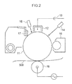
- Fig. 2 is a cross-sectional view depicting an outline of a basic configuration of an example of the image forming apparatus of the exemplary embodiment.
- the image forming apparatus shown in Fig. 2 includes a photoreceptor 11 of the exemplary embodiment as described above; a charging device 12 of contact charging type that charges the photoreceptor 11; a power supply 13 connected to the charging device 12; an exposure device 14 that exposes the photoreceptor 11 charged by the charging device 12, to form an electrostatic latent image; a developing device 15 that develops the electrostatic latent image formed by the exposure device 14 using a toner, to form a toner image; a transfer device 16 that transfers the toner image formed by the developing device 15 to a recording medium 500; a cleaning device 17; and a charge eraser 18.
- the image forming apparatus may be the apparatus that is not provided with the charge eliminating device 18.
- the charging device 12 is a non-contact type charging device that applies a voltage to the photoreceptor 11 without contacting with the surface of the photoreceptor 11, and charges the surface of the photoreceptor 11 to a predetermined potential.
- a non-contact type charge device such as a corotron or a scorotron may be used.
- an optical device capable of required-imagewise light exposure using a light source such as a semiconductor laser, a light emitting diode (LED) or a liquid crystal shutter, on the surface of the photoreceptor 11, or the like, may be used.
- a light source such as a semiconductor laser, a light emitting diode (LED) or a liquid crystal shutter, on the surface of the photoreceptor 11, or the like.
- the developing device 15 a conventionally known developing device using a normal or reversal developer such as of a one-component system or a two-component system, is used.
- the shape of the toner used in the developing device 15 is not particularly limited, and a toner having an irregular shape, a spherical shape, or even some other specific shape may be used.
- the transfer device 16 may be a roller-shaped contact type transfer charging member; a contact type transfer charging unit using a belt, a film, a rubber blade or the like; a scorotron transfer charging unit or corotron transfer charging unit utilizing corona discharge; or the like.
- the cleaning device 17 is a device for removing any residual toner, paper dust or the like, which remains attached to the surface of the photoreceptor 11 after the transfer process, and the photoreceptor 11 having the surface cleaned by this cleaning device is repeatedly used for the image forming process described above.
- a cleaning blade, brush cleaning, roll cleaning and the like may be used, and among these, it is preferable to use a cleaning blade.
- the material of the cleaning blade include urethane rubber, neoprene rubber, silicone rubber, and the like.
- the image forming apparatus of the exemplary embodiment may further include an erasing light irradiation device as the charge eraser 18, as shown in Fig. 2 .
- an erasing light irradiation device as the charge eraser 18, as shown in Fig. 2 .
- a brush, film or the like having a charge erasing ability may also be used instead. This allows, when the photoreceptor 11 is repeatedly uesed, prevention of the phenomenon of the residual potential of the photoreceptor 11 being carried over to the subsequent cycles.
- FIG. 3 is a cross-sectional view depicting an outline of a basic configuration of another example of the image forming apparatus of the exemplary embodiment.
- the image forming apparatus 400 shown in Fig. 3 is a so-called four-cycle type image forming apparatus, which forms a toner image of multiple colors with a single electrophotographic photoreceptor.
- the image forming apparatus 400 includes a photoreceptor drum 401 which rotates in the direction of the arrow A in the drawing at a predetermined speed of rotation under the action of a driving unit (not depicted), and a charging device 422 that charges the outer peripheral surface of the photoreceptor drum 401 is provided above the photoreceptor drum 401.
- an exposure device 430 including a surface emitting laser array as an exposure light source.
- the exposure device 430 modulates plural laser beams that are ejected from the light source in accordance with the image to be formed, and also deflects the laser beams to the main scanning direction so as to scan over the outer peripheral surface of the photoreceptor drum 401 in parallel with the axial line of the photoreceptor drum 401. Thereby, an electrostatic latent image is formed on the outer peripheral surface of the charged photoreceptor drum 401.
- a developing device 425 is disposed laterally to the photoreceptor drum 401.
- the developing device 425 includes a roller-shaped holder that is disposed to be rotatable. There are four holding units formed in the inside of this holder, and each holding unit is provided with a developing unit 425Y, 425M, 425C or 425K.
- the developing units 425Y, 425M, 425C and 425K each include a developing roller 426, and respectively store a toner having a color of yellow (Y), magenta (M), cyan (C) and black (K) inside the developing unit.
- Formation of full color images in the image forming apparatus 400 is carried out by the formation of an image by the photoreceptor drum 401 four times.
- the charging device 422 repeats charging of the outer peripheral surface of the photoreceptor drum 401 every time the photoreceptor drum 401 forms an image once.
- the exposure device 430 repeats scanning the laser beam which has been modulated in accordance with any of the image data of Y, M, C and K colors representing the color image to be formed, over the outer peripheral surface of the photoreceptor drum 401, while converting the image data used in the modulation of the laser beam, every time the photoreceptor drum 401 forms an image once.
- the developing device 425 repeats operating a developing unit that is facing the outer peripheral surface, with the developing roller 426 of any of the developing units 425Y, 425M, 425C and 425K facing the outer peripheral surface of the photoreceptor drum 401, to develop the electrostatic latent image formed on the outer peripheral surface of the photoreceptor drum 401 in determined colors, and to form a toner image of the colors on the outer peripheral surface of the photoreceptor drum 401, every time the photoreceptor drum 401 forms an image of each color, while rotating the holder so as to change the developing unit used in the development of the electrostatic latent image.
- the photoreceptor drum 401 forms an image of each color
- toner images of Y, M, C and K colors are sequentially formed on the outer peripheral surface of the photoreceptor drum 401.
- an endless intermediate transfer belt 450 is disposed below the photoreceptor drum 401.
- the intermediate transfer belt 450 is stretched over rollers 451, 453 and 455, and is disposed such that the outer peripheral surface is in contact with the outer peripheral surface of the photoreceptor drum 401.
- the rollers 451, 453 and 455 rotate as a result of the driving force of the motor, which is not depicted in the drawing, being transferred, and make the intermediate transfer belt 450 to revolve in the direction of the arrow B in Fig. 3 .
- a transfer device (transfer unit) 440 is disposed, and the toner images of Y, M, C and K colors that have been sequentially formed on the outer peripheral surface of the photoreceptor drum 401, are transferred to the image forming surface of the intermediate transfer belt 450, one color at a time, by the transfer device 440. Eventually, all of the images of Y, M, C and K colors are disposed on the intermediate transfer belt 450.
- a lubricant supplying device 428 and a cleaning device 427 are disposed on the outer peripheral surface of the photoreceptor drum 401.
- a lubricant is supplied to the outer peripheral surface of the photoreceptor drum 401 by the lubricant supplying device 428, and in the outer peripheral surface, the area in which toner images were held and then transferred is cleaned by the cleaning device 427.
- a transfer medium holding unit 460 is disposed below the intermediate transfer belt 450, and a large number of sheets of paper 500 as a recording medium are stacked and held inside the transfer medium holding unit 460.
- a takeout roller 461 is disposed, and on the downstream side in the direction of takeout of the paper 500 by the takeout roller 461, a pair of rollers 463 and a roller 465 are disposed in order.
- a sheet of paper (recording medium) 500 that is stacked and located on the uppermost side, is taken out from the transfer medium holding unit 460 as the takeout roller 461 rotates, and is conveyed by the pair of rollers 463 and the roller 465.
- a transfer device 442 is disposed on the opposite side of the roller 455 with respect to the intermediate transfer belt 450.
- the paper 500 conveyed by the pair of rollers 463 and the roller 465 is conveyed to an area interposed between the intermediate transfer belt 450 and the transfer device 442, and the toner image formed on the image forming surface of the intermediate transfer belt 450 is transferred to the paper 500 by the transfer device 442.
- a fixing device 444 equipped with a pair of fixing rollers is disposed on the downstream side with respect to the transfer device 442 in the direction of conveyance of the paper 500.
- the paper 500 having the toner image transferred thereon is discharged out of the image forming apparatus 400 after the transferred toner image is subjected fusion fixing by the fixing device 444, and the paper is placed on the catch tray (not depicted).
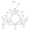
- FIG. 4 is a cross-sectional view depicting an outline of a basic configuration of an example of the process cartridge of the exemplary embodiment.
- the process cartridge 300 includes a photoreceptor 307, a charging device 308, a developing device 311, a cleaning device 313, an aperture 318 for exposure, and an aperture 317 for exposure after elimination of charge, which are combined and integrated using a mounting rail 316.
- This process cartridge 300 is freely attachable to and detachable from the main body of the image forming apparatus which includes a transfer device 312, a fixing device 315 and other constituent elements that are not depicted, and constitutes the image forming apparatus together with the body of the image forming apparatus and the like.
- the recording medium 500 that is used in the exemplary embodiment is not particularly limited as long as it is a medium capable of receiving the toner image formed on the photoreceptor and transferred.
- the paper is the recording medium.
- the intermediate transfer medium is the recording medium.
- This coating liquid is applied on an aluminum substrate having a diameter of 84 mm, a length of 340 mm and a thickness of 1 mm, by a dip coating method, and the substrate is subjected to drying and curing at 160°C for 100 minutes, to obtain an intermediate layer having a thickness of 20 ⁇ m.
- the resulting dispersion liquid is dip-coated on the intermediate layer and dried at 100°C for 10 minutes, to form a charge generating layer having a thickness of 0.2 ⁇ m.
- a coating liquid is prepared by sufficiently mixing and dissolving 45 parts by N,N'-bis(3-methylphenyl)-N,N'-diphenylbenzidine and 55 parts by weight of bisphenol Z-polycarbonate resin (trade name: TS2050, viscosity average molecular weight 50,000, manufactured by Teijin Chemicals, Ltd.) in 300 parts by weight of tetrahydrofuran and 100 parts by weight of monochlorobenzene, and this coating liquid is dip-coated, as a charge transporting layer, on the aluminum substrate having up to the charge generating layer formed thereon.
- the coating liquid is dried at 125°C for 60 minutes, to form a charge transporting layer having a thickness of 19 ⁇ m.
- the obtained photoreceptor is mounted on a DOCUCENTRE COLOR500 (trade name) manufactured by Fuji Xerox Corp., and 10,000 sheets per day of a full-page halftone image at a density of 40% are printed under high temperature and high humidity conditions at 29°C and 80% RH. It is verified whether image degradation occurs in every 1000 th sheet of the printed images. Furthermore, the photoreceptor is left to stand under high temperature and high humidity for 14 hours, and the first print after a lapse of 14 hours is carried out by printing a full-page halftone image at a density of 40%. Thus, the image degradation after standing is checked. The results are shown in Table 3. The evaluation criteria are as follows.
- the residual potential is measured by the following method, and evaluation is carried out.
- the residual potential is measured after printing the first sheet and the 10,000 th sheet of a full-page halftone image at a density of 40%, using a surface potentiometer installed in the DOCUCENTRE COLOR 500, separately under high temperature and high humidity conditions at 29°C and 80% RH and under low temperature and low humidity conditions at 10°C and 20% RH.
- the differences are determined, and the absolute values of the differences are taken as the amount of change of the residual potential.
- the amount of change of the residual potential is evaluated according to the following criteria. The results are shown in Table 3.
- the evaluation criteria are as follows.
- the ionization potential of the various materials is measured using a photoelectron spectroscopy in air, AC-2 (trade name) manufactured by Riken Keiki Co., Ltd., as described above.
- the ionization potentials are shown in the following Table 1.
- An intermediate layer, a charge generating layer and a charge transporting layer are formed according to the method described in Example 1. Subsequently, a surface layer is formed by the same method as described in Example 1, except that the charge transporting material indicated in Table 1 or Table 2 is used correspondingly, the content of the material and the layer thickness are correspondingly changed to the respective values indicated in Table 1 or Table 2.
- the amount of the solvent t-BuOH is adjusted, and coating is carried out. The evaluation is carried out in the same manner as in Example 1.
- Example 1 Charge transporting material 1 Charge transporting material 2 Charge transporting material 3 Melamine Thickness ( ⁇ m) Type Content X [parts by [weight] Ionization potential Type Content X [parts by weight] Ionization potential Type Content X [parts by weight] Ionization potential
- Example 1 1-21 55 5.70 1-19 43 5.53 - 0 - 2 6
- Example 2 1-21 60 5.70 1-19 38 5.53 - 0 - 2 6
- Example 3 1-21 65 5.70 1-19 33 5.53 - 0 - 2 6
- Example 4 1-21 55 5.70 1-19 43 5.53 - 0 - 2 10
- Example 5 1-21 55 5.70 1-19 43 5.53 - 0 - 2 15
- Example 6 1-21 55 5.70 1-19 43 5.53 - 0 - 2 17
- Example 7 1-21 56 5.70 1-27 41 5.44 - 0 - 3 6
- Example 8 1-21 55 5.70 1-27 40 5.44 - 0 - 5 6
- Example 9 1-8 42 5.77
Landscapes
- Physics & Mathematics (AREA)
- General Physics & Mathematics (AREA)
- Spectroscopy & Molecular Physics (AREA)
- Chemical & Material Sciences (AREA)
- Chemical Kinetics & Catalysis (AREA)
- Inorganic Chemistry (AREA)
- Photoreceptors In Electrophotography (AREA)
Applications Claiming Priority (1)
| Application Number | Priority Date | Filing Date | Title |
|---|---|---|---|
| JP2009152541A JP5428574B2 (ja) | 2009-06-26 | 2009-06-26 | 電子写真感光体、画像形成装置、およびプロセスカートリッジ |
Publications (2)
| Publication Number | Publication Date |
|---|---|
| EP2267543A2 true EP2267543A2 (de) | 2010-12-29 |
| EP2267543A3 EP2267543A3 (de) | 2011-11-09 |
Family
ID=42790910
Family Applications (1)
| Application Number | Title | Priority Date | Filing Date |
|---|---|---|---|
| EP10156225A Withdrawn EP2267543A3 (de) | 2009-06-26 | 2010-03-11 | Elektrofotografischer Fotorezeptor, Bilderzeugungsvorrichtung und Prozesskartusche |
Country Status (4)
| Country | Link |
|---|---|
| US (1) | US8685600B2 (de) |
| EP (1) | EP2267543A3 (de) |
| JP (1) | JP5428574B2 (de) |
| CN (1) | CN101930187B (de) |
Families Citing this family (9)
| Publication number | Priority date | Publication date | Assignee | Title |
|---|---|---|---|---|
| JP5724518B2 (ja) * | 2011-03-28 | 2015-05-27 | 富士ゼロックス株式会社 | 電子写真感光体、画像形成装置、およびプロセスカートリッジ |
| JP2013057810A (ja) * | 2011-09-08 | 2013-03-28 | Fuji Xerox Co Ltd | 電子写真感光体、電子写真感光体の製造方法、画像形成装置、およびプロセスカートリッジ |
| JP5807507B2 (ja) * | 2011-10-20 | 2015-11-10 | 富士ゼロックス株式会社 | 電子写真感光体、プロセスカートリッジ、及び画像形成装置 |
| JP5866991B2 (ja) * | 2011-11-14 | 2016-02-24 | 富士ゼロックス株式会社 | 画像形成装置 |
| JP2013200415A (ja) * | 2012-03-23 | 2013-10-03 | Fuji Xerox Co Ltd | 電子写真感光体、プロセスカートリッジ、及び画像形成装置 |
| JP5900277B2 (ja) | 2012-03-23 | 2016-04-06 | 富士ゼロックス株式会社 | 電子写真感光体、プロセスカートリッジ、及び画像形成装置 |
| JP5954040B2 (ja) * | 2012-08-10 | 2016-07-20 | 富士ゼロックス株式会社 | 電子写真感光体、プロセスカートリッジ、及び画像形成装置 |
| JP6024334B2 (ja) * | 2012-09-21 | 2016-11-16 | 富士ゼロックス株式会社 | 画像形成装置、およびプロセスカートリッジ |
| US10178447B2 (en) | 2015-07-23 | 2019-01-08 | Palo Alto Research Center Incorporated | Sensor network system |
Citations (10)
| Publication number | Priority date | Publication date | Assignee | Title |
|---|---|---|---|---|
| JPS5651749A (en) | 1979-10-04 | 1981-05-09 | Canon Inc | Electrophotographic receptor |
| JPS60247647A (ja) | 1984-05-23 | 1985-12-07 | Canon Inc | 静電荷像形成方法 |
| JPS641728A (en) | 1987-06-10 | 1989-01-06 | Xerox Corp | Arylamine-containing polyhydroxyether resin |
| JPH04281461A (ja) | 1991-03-08 | 1992-10-07 | Ricoh Co Ltd | 電子写真用感光体 |
| JPH08278645A (ja) | 1995-04-07 | 1996-10-22 | Ricoh Co Ltd | 電子写真感光体 |
| JP2000292959A (ja) | 1999-04-02 | 2000-10-20 | Nec Corp | 電子写真感光体 |
| JP2001255685A (ja) | 2000-03-13 | 2001-09-21 | Konica Corp | 電子写真感光体、画像形成方法、画像形成装置、及びプロセスカートリッジ |
| JP2002082469A (ja) | 2000-06-21 | 2002-03-22 | Canon Inc | 電子写真感光体、電子写真装置およびプロセスカートリッジ |
| JP2003186234A (ja) | 2001-12-21 | 2003-07-03 | Canon Inc | 電子写真感光体、該電子写真感光体を有するプロセスカートリッジ及び電子写真装置 |
| JP2003186222A (ja) | 2001-12-21 | 2003-07-03 | Canon Inc | 電子写真感光体、該電子写真感光体を有するプロセスカートリッジ及び電子写真装置 |
Family Cites Families (76)
| Publication number | Priority date | Publication date | Assignee | Title |
|---|---|---|---|---|
| US5358813A (en) * | 1902-01-13 | 1994-10-25 | Fuji Xerox Co., Ltd. | Crystals of chlorogallium phthalocyanine and method of preparing them |
| JP3123185B2 (ja) | 1991-04-22 | 2001-01-09 | 富士ゼロックス株式会社 | クロロガリウムフタロシアニンの新規な結晶、その新規な結晶よりなる光導電材料及びそれを用いた電子写真感光体 |
| JPS62251757A (ja) | 1986-04-24 | 1987-11-02 | Hitachi Chem Co Ltd | 正帯電型電子写真感光体 |
| US4956440A (en) * | 1987-06-10 | 1990-09-11 | Xerox Corporation | Arylamine containing polyhydroxyether resins |
| AU611070B2 (en) | 1988-12-26 | 1991-05-30 | Mitsui Toatsu Chemicals Inc. | Injection-molding thermosetting resin composition |
| JPH02255856A (ja) | 1988-12-26 | 1990-10-16 | Mitsui Toatsu Chem Inc | 射出成形用熱硬化性樹脂組成成物 |
| US5290928A (en) * | 1990-11-22 | 1994-03-01 | Fuji Xerox Co., Ltd. | Process for preparing oxytitanium phthalocyanine hydrate crystal |
| JPH04189873A (ja) * | 1990-11-22 | 1992-07-08 | Fuji Xerox Co Ltd | オキシチタニウムフタロシアニン水和物結晶及びそれを用いた電子写真感光体 |
| JP3166293B2 (ja) * | 1991-04-26 | 2001-05-14 | 富士ゼロックス株式会社 | ヒドロキシガリウムフタロシアニンの新規な結晶、その新規な結晶よりなる光導電材料およびそれを用いた電子写真感光体 |
| US5393629A (en) * | 1991-04-26 | 1995-02-28 | Fuji Xerox Co., Ltd. | Electrophotographic photoreceptor |
| JP3092270B2 (ja) | 1991-11-15 | 2000-09-25 | 富士ゼロックス株式会社 | 新規なジクロロスズフタロシアニン結晶の製造方法及びその結晶を用いた電子写真感光体 |
| US5283145A (en) * | 1991-05-01 | 1994-02-01 | Fuji Xerox Co., Ltd. | Crystals of dichlorotin phthalocyanine, method of preparing the crystal, and electrophotographic photoreceptor comprising the crystal |
| JPH0543823A (ja) | 1991-08-12 | 1993-02-23 | Fuji Resin Kogyo Kk | 導電性コーテイング材 |
| US5308728A (en) * | 1991-08-16 | 1994-05-03 | Fuji Xerox Co., Ltd. | Dichlorotin phthalocyanine crystal, process for producing the same, and electrophotographic photoreceptor using the same |
| US5338636A (en) * | 1991-09-27 | 1994-08-16 | Fuji Xerox Co., Ltd. | Dichlorotin phthalocyanine crystal electrophotographic photoreceptor using the same, and coating composition for electrophotographic photoreceptor |
| JP3123184B2 (ja) | 1991-09-27 | 2001-01-09 | 富士ゼロックス株式会社 | ジクロロスズフタロシアニンの新規な結晶とその製造方法、およびそれを用いた電子写真感光体 |
| JPH0599737A (ja) | 1991-10-10 | 1993-04-23 | Mitsubishi Kasei Corp | 光量センサー |
| JP3166283B2 (ja) | 1992-03-31 | 2001-05-14 | 富士ゼロックス株式会社 | ヒドロキシガリウムフタロシアニンの新規な結晶の製造方法 |
| JP3287678B2 (ja) | 1992-12-28 | 2002-06-04 | キヤノン株式会社 | 電子写真感光体、該電子写真感光体を有する電子写真装置及び装置ユニット |
| JPH07146564A (ja) | 1993-11-24 | 1995-06-06 | Fuji Electric Co Ltd | 電子写真感光体 |
| JP2865029B2 (ja) | 1994-10-24 | 1999-03-08 | 富士ゼロックス株式会社 | 電荷輸送性ポリエステルを用いた有機電子デバイス |
| US5639581A (en) * | 1994-10-24 | 1997-06-17 | Fuji Xerox Co., Ltd. | Charge transporting polymer, process for producing the same, and organic electronic device containing the same |
| JP2894257B2 (ja) | 1994-10-24 | 1999-05-24 | 富士ゼロックス株式会社 | 新規電荷輸送性ポリマー、その製造法およびそれを用いた有機電子デバイス |
| US5654119A (en) * | 1995-04-06 | 1997-08-05 | Fuji Xerox Co., Ltd. | Organic electronic device comprising charge-transporting polyester and image forming apparatus |
| US5932384A (en) * | 1997-05-14 | 1999-08-03 | Mitsubishi Chemical Corporation | Electrophotographic photoreceptor |
| JP4011790B2 (ja) | 1998-06-12 | 2007-11-21 | キヤノン株式会社 | 電子写真感光体の製造方法 |
| EP0964309B1 (de) * | 1998-06-12 | 2005-12-07 | Canon Kabushiki Kaisha | Elektrophotographisches, lichtempfindliches Element, Verfahrenskassette und elektrophotographischer Apparat, sowie Verfahren zur Herstellung des lichtempfindlichen Elementes |
| JP3755856B2 (ja) | 1998-06-26 | 2006-03-15 | キヤノン株式会社 | 電子写真感光体 |
| US6489069B1 (en) * | 1999-02-15 | 2002-12-03 | Konica Corporation | Electrophotographic image carrier and image forming apparatus, image forming method and processing cartridge using it |
| JP2001201876A (ja) | 2000-01-17 | 2001-07-27 | Ricoh Co Ltd | 電子写真感光体及びそれを用いた画像形成方法 |
| EP1174771B1 (de) * | 2000-06-21 | 2008-06-11 | Canon Kabushiki Kaisha | Elektrophotographisches photoempfindliches Element, Prozesskartusche und elektrophotographischer Apparat |
| JP2002006524A (ja) | 2000-06-23 | 2002-01-09 | Hitachi Chem Co Ltd | 電子写真感光体 |
| JP3766008B2 (ja) * | 2000-11-30 | 2006-04-12 | 株式会社リコー | 電子写真感光体、その製造方法、電子写真方法、画像形成装置及び画像形成装置用プロセスカートリッジ |
| US6830858B2 (en) * | 2001-06-27 | 2004-12-14 | Ricoh Company, Ltd. | Electrophotographic photosensitive member, preparation method thereof, image forming process, apparatus and process cartridge using the same |
| JP3963440B2 (ja) | 2001-06-27 | 2007-08-22 | 株式会社リコー | 電子写真感光体及びその製造方法、並びに該電子写真感光体を用いた画像形成方法、画像形成装置、及び画像形成用プロセスカートリッジ |
| US6829454B2 (en) * | 2001-08-28 | 2004-12-07 | Seiko Epson Corporation | Image forming apparatus with improved transfer efficiency |
| US6806009B2 (en) * | 2001-12-21 | 2004-10-19 | Canon Kabushiki Kaisha | Electrophotographic photosensitive member, process cartridge and electrophotographic apparatus |
| JP3979243B2 (ja) | 2002-04-24 | 2007-09-19 | コニカミノルタホールディングス株式会社 | 有機感光体、画像形成方法、画像形成装置及びプロセスカートリッジ |
| CN1310096C (zh) * | 2002-07-15 | 2007-04-11 | 佳能株式会社 | 电摄影感光体、电摄影装置和成像处理盒 |
| JP4050176B2 (ja) * | 2003-04-04 | 2008-02-20 | シャープ株式会社 | 電子写真感光体およびそれを備える画像形成装置 |
| JP4148415B2 (ja) | 2003-07-31 | 2008-09-10 | 株式会社リコー | 電子写真感光体、電子写真装置、及びプロセスカートリッジ |
| JP4070700B2 (ja) | 2003-10-01 | 2008-04-02 | 株式会社リコー | 電子写真感光体、画像形成装置、画像形成装置用プロセスカートリッジ |
| JP3881648B2 (ja) * | 2003-10-08 | 2007-02-14 | シャープ株式会社 | 電子写真感光体およびそれを備える画像形成装置 |
| JP4319553B2 (ja) | 2004-01-08 | 2009-08-26 | 株式会社リコー | 電子写真感光体、電子写真感光体の製造方法、電子写真装置、プロセスカートリッジ |
| JP4410691B2 (ja) | 2004-01-19 | 2010-02-03 | 株式会社リコー | 電子写真感光体、それを用いた画像形成方法、画像形成装置及び画像形成装置用プロセスカートリッジ |
| JP4228932B2 (ja) | 2004-02-18 | 2009-02-25 | 富士ゼロックス株式会社 | 電子写真感光体、プロセスカートリッジ及び電子写真装置 |
| JP2005234081A (ja) | 2004-02-18 | 2005-09-02 | Konica Minolta Business Technologies Inc | 画像形成装置及び画像形成方法 |
| EP1600822B1 (de) | 2004-05-25 | 2018-12-12 | Ricoh Company, Ltd. | Elektrophotographischer photorezeptor,bilderzeugungsverfahren, bilderzeugungs-apparat und prozesskartusche |
| JP2006084711A (ja) * | 2004-09-15 | 2006-03-30 | Fuji Xerox Co Ltd | 電子写真感光体用添加物、電子写真感光体、画像形成装置及びプロセスカートリッジ |
| US20060093931A1 (en) * | 2004-11-04 | 2006-05-04 | Akihiko Itami | Organic photoconductor, image forming method, image forming apparatus and process cartridge |
| US20060199092A1 (en) * | 2005-03-03 | 2006-09-07 | Akihiro Sugino | Electrostatic latent image bearer, and image forming method, image forming apparatus and process cartridge using the electrostatic latent image bearer |
| JP4595603B2 (ja) * | 2005-03-16 | 2010-12-08 | 富士ゼロックス株式会社 | 画像形成装置 |
| JP2006267652A (ja) | 2005-03-24 | 2006-10-05 | Fuji Xerox Co Ltd | 電子写真感光体、プロセスカートリッジ及び画像形成装置 |
| JP2006276103A (ja) | 2005-03-28 | 2006-10-12 | Fuji Xerox Co Ltd | 画像形成装置 |
| JP2007086209A (ja) | 2005-09-20 | 2007-04-05 | Fuji Xerox Co Ltd | 画像形成装置及び画像形成方法 |
| JP4600230B2 (ja) * | 2005-09-21 | 2010-12-15 | 富士ゼロックス株式会社 | 電子写真感光体、プロセスカートリッジ及び画像形成装置 |
| US7384717B2 (en) * | 2005-09-26 | 2008-06-10 | Xerox Corporation | Photoreceptor with improved overcoat layer |
| JP4590344B2 (ja) * | 2005-11-21 | 2010-12-01 | 株式会社リコー | 静電潜像担持体及びそれを用いた画像形成装置、プロセスカートリッジ及び画像形成方法 |
| JP4615426B2 (ja) | 2005-12-01 | 2011-01-19 | 株式会社リコー | 画像形成装置及び画像形成方法 |
| JP4807848B2 (ja) | 2005-12-15 | 2011-11-02 | 株式会社リコー | 画像形成装置及び画像形成方法 |
| JP4885535B2 (ja) * | 2005-12-26 | 2012-02-29 | 富士ゼロックス株式会社 | 電子写真感光体、プロセスカートリッジ及び画像形成装置 |
| US8029956B2 (en) * | 2006-01-13 | 2011-10-04 | Xerox Corporation | Photoreceptor with overcoat layer |
| JP2007219087A (ja) * | 2006-02-15 | 2007-08-30 | Fuji Xerox Co Ltd | 帯電装置及び画像形成装置 |
| US7674565B2 (en) * | 2006-07-25 | 2010-03-09 | Xerox Corporation | Protective overcoat |
| JP4800157B2 (ja) * | 2006-09-15 | 2011-10-26 | 株式会社リコー | 電子写真感光体並びに電子写真装置 |
| JP2008096923A (ja) * | 2006-10-16 | 2008-04-24 | Fuji Xerox Co Ltd | 画像形成装置及びプロセスカートリッジ |
| US7645548B2 (en) | 2006-11-06 | 2010-01-12 | Xerox Corporation | Photoreceptor overcoat layer masking agent |
| JP2008299039A (ja) * | 2007-05-31 | 2008-12-11 | Fuji Xerox Co Ltd | 画像形成装置 |
| US8679709B2 (en) * | 2007-06-28 | 2014-03-25 | Fuji Xerox Co., Ltd. | Electrophotographic photoreceptor, process cartridge, image forming apparatus, and film forming coating solution |
| JP2009063862A (ja) * | 2007-09-07 | 2009-03-26 | Fuji Xerox Co Ltd | 帯電装置、プロセスカートリッジ、画像形成装置、およびクリーニング部材 |
| US8309285B2 (en) * | 2007-11-07 | 2012-11-13 | Xerox Corporation | Protective overcoat layer and photoreceptor including same |
| JP4618311B2 (ja) * | 2008-03-19 | 2011-01-26 | 富士ゼロックス株式会社 | 電子写真感光体、プロセスカートリッジ、及び画像形成装置 |
| US8273511B2 (en) | 2008-12-25 | 2012-09-25 | Fuji Xerox Co., Ltd. | Electrophotographic photoreceptor, manufacturing method of electrophotographic photoreceptor, processing cartridge, and image forming apparatus |
| JP2010224173A (ja) * | 2009-03-23 | 2010-10-07 | Fuji Xerox Co Ltd | 電子写真感光体、プロセスカートリッジ、及び画像形成装置 |
| JP4900413B2 (ja) | 2009-03-27 | 2012-03-21 | 富士ゼロックス株式会社 | 画像形成装置、及びプロセスカートリッジ |
| JP2011008117A (ja) * | 2009-06-26 | 2011-01-13 | Fuji Xerox Co Ltd | 電子写真感光体、プロセスカートリッジ、及び画像形成装置 |
-
2009
- 2009-06-26 JP JP2009152541A patent/JP5428574B2/ja not_active Expired - Fee Related
- 2009-11-23 US US12/623,916 patent/US8685600B2/en active Active
- 2009-12-07 CN CN2009102533531A patent/CN101930187B/zh active Active
-
2010
- 2010-03-11 EP EP10156225A patent/EP2267543A3/de not_active Withdrawn
Patent Citations (10)
| Publication number | Priority date | Publication date | Assignee | Title |
|---|---|---|---|---|
| JPS5651749A (en) | 1979-10-04 | 1981-05-09 | Canon Inc | Electrophotographic receptor |
| JPS60247647A (ja) | 1984-05-23 | 1985-12-07 | Canon Inc | 静電荷像形成方法 |
| JPS641728A (en) | 1987-06-10 | 1989-01-06 | Xerox Corp | Arylamine-containing polyhydroxyether resin |
| JPH04281461A (ja) | 1991-03-08 | 1992-10-07 | Ricoh Co Ltd | 電子写真用感光体 |
| JPH08278645A (ja) | 1995-04-07 | 1996-10-22 | Ricoh Co Ltd | 電子写真感光体 |
| JP2000292959A (ja) | 1999-04-02 | 2000-10-20 | Nec Corp | 電子写真感光体 |
| JP2001255685A (ja) | 2000-03-13 | 2001-09-21 | Konica Corp | 電子写真感光体、画像形成方法、画像形成装置、及びプロセスカートリッジ |
| JP2002082469A (ja) | 2000-06-21 | 2002-03-22 | Canon Inc | 電子写真感光体、電子写真装置およびプロセスカートリッジ |
| JP2003186234A (ja) | 2001-12-21 | 2003-07-03 | Canon Inc | 電子写真感光体、該電子写真感光体を有するプロセスカートリッジ及び電子写真装置 |
| JP2003186222A (ja) | 2001-12-21 | 2003-07-03 | Canon Inc | 電子写真感光体、該電子写真感光体を有するプロセスカートリッジ及び電子写真装置 |
Also Published As
| Publication number | Publication date |
|---|---|
| JP2011008099A (ja) | 2011-01-13 |
| CN101930187B (zh) | 2013-07-03 |
| US20100330472A1 (en) | 2010-12-30 |
| CN101930187A (zh) | 2010-12-29 |
| EP2267543A3 (de) | 2011-11-09 |
| JP5428574B2 (ja) | 2014-02-26 |
| US8685600B2 (en) | 2014-04-01 |
Similar Documents
| Publication | Publication Date | Title |
|---|---|---|
| EP2267543A2 (de) | Elektrofotografischer Fotorezeptor, Bilderzeugungsvorrichtung und Prozesskartusche | |
| JP2006084711A (ja) | 電子写真感光体用添加物、電子写真感光体、画像形成装置及びプロセスカートリッジ | |
| JP4905228B2 (ja) | 電子写真感光体、プロセスカートリッジ及び画像形成装置 | |
| JP2015078350A (ja) | ポリアリレート樹脂、及びそれを用いた電子写真感光体 | |
| JP2008216812A (ja) | 電子写真感光体、プロセスカートリッジ及び画像形成装置 | |
| WO2014021341A1 (ja) | 電子写真感光体、電子写真感光体カートリッジ、画像形成装置、及びトリアリールアミン化合物 | |
| JP2007133344A (ja) | 電荷輸送性化合物、電子写真感光体、画像形成装置及びプロセスカートリッジ | |
| JP4885535B2 (ja) | 電子写真感光体、プロセスカートリッジ及び画像形成装置 | |
| JP2008015275A (ja) | 電子写真感光体、画像形成装置及びプロセスカートリッジ | |
| JP2003287914A (ja) | 電子写真感光体、画像形成装置、画像形成方法及びプロセスカートリッジ | |
| JP5315851B2 (ja) | ポリカーボネート樹脂、それを用いた電子写真感光体用塗布液及び電子写真感光体 | |
| JP2003307861A (ja) | 有機感光体、画像形成方法、画像形成装置、及びプロセスカートリッジ | |
| JP7005327B2 (ja) | 電子写真感光体、プロセスカートリッジ及び電子写真装置 | |
| JP2009237165A (ja) | 電子写真感光体、プロセスカートリッジ及び画像形成装置 | |
| JP4285212B2 (ja) | 電子写真感光体用添加剤、電子写真感光体、画像形成装置及びプロセスカートリッジ | |
| JP4360288B2 (ja) | 電子写真感光体、画像形成装置及びプロセスカートリッジ | |
| JP3952833B2 (ja) | 有機感光体、画像形成方法、画像形成装置及びプロセスカートリッジ | |
| JP2008262050A (ja) | 電子写真感光体、プロセスカートリッジ、及び画像形成装置 | |
| JP5049059B2 (ja) | 電子写真感光体、並びにこれを用いた画像形成装置及びプロセスカートリッジ | |
| JP2009075341A (ja) | 電子写真感光体、プロセスカートリッジ、及び画像形成装置 | |
| JP4696905B2 (ja) | 電子写真用有機感光体及び画像形成装置 | |
| JP6307885B2 (ja) | 電子写真感光体、電子写真感光体カートリッジ、及び画像形成装置 | |
| JP4400288B2 (ja) | 電子写真感光体、該電子感光体を用いたドラムカートリッジおよび画像形成装置 | |
| JP5365262B2 (ja) | 電子写真感光体、プロセスカートリッジ及び画像形成装置 | |
| JP5353083B2 (ja) | 電子写真感光体および該感光体を用いた画像形成装置 |
Legal Events
| Date | Code | Title | Description |
|---|---|---|---|
| PUAI | Public reference made under article 153(3) epc to a published international application that has entered the european phase |
Free format text: ORIGINAL CODE: 0009012 |
|
| AK | Designated contracting states |
Kind code of ref document: A2 Designated state(s): AT BE BG CH CY CZ DE DK EE ES FI FR GB GR HR HU IE IS IT LI LT LU LV MC MK MT NL NO PL PT RO SE SI SK SM TR |
|
| AX | Request for extension of the european patent |
Extension state: AL BA ME RS |
|
| PUAL | Search report despatched |
Free format text: ORIGINAL CODE: 0009013 |
|
| AK | Designated contracting states |
Kind code of ref document: A3 Designated state(s): AT BE BG CH CY CZ DE DK EE ES FI FR GB GR HR HU IE IS IT LI LT LU LV MC MK MT NL NO PL PT RO SE SI SK SM TR |
|
| AX | Request for extension of the european patent |
Extension state: AL BA ME RS |
|
| RIC1 | Information provided on ipc code assigned before grant |
Ipc: G03G 5/147 20060101ALI20110930BHEP Ipc: G03G 5/14 20060101ALI20110930BHEP Ipc: G03G 5/06 20060101ALI20110930BHEP Ipc: G03G 5/05 20060101AFI20110930BHEP |
|
| 17P | Request for examination filed |
Effective date: 20120502 |
|
| STAA | Information on the status of an ep patent application or granted ep patent |
Free format text: STATUS: THE APPLICATION HAS BEEN WITHDRAWN |
|
| 18W | Application withdrawn |
Effective date: 20140117 |