EP2267787A2 - Méthode de fabrication d'un transistor à effet de champ DMOS à grille en tranchée - Google Patents
Méthode de fabrication d'un transistor à effet de champ DMOS à grille en tranchée Download PDFInfo
- Publication number
- EP2267787A2 EP2267787A2 EP10012844A EP10012844A EP2267787A2 EP 2267787 A2 EP2267787 A2 EP 2267787A2 EP 10012844 A EP10012844 A EP 10012844A EP 10012844 A EP10012844 A EP 10012844A EP 2267787 A2 EP2267787 A2 EP 2267787A2
- Authority
- EP
- European Patent Office
- Prior art keywords
- trench
- layer
- insulating layer
- over
- region
- Prior art date
- Legal status (The legal status is an assumption and is not a legal conclusion. Google has not performed a legal analysis and makes no representation as to the accuracy of the status listed.)
- Granted
Links
Images


Classifications
-
- H—ELECTRICITY
- H10—SEMICONDUCTOR DEVICES; ELECTRIC SOLID-STATE DEVICES NOT OTHERWISE PROVIDED FOR
- H10D—INORGANIC ELECTRIC SEMICONDUCTOR DEVICES
- H10D30/00—Field-effect transistors [FET]
- H10D30/60—Insulated-gate field-effect transistors [IGFET]
-
- H—ELECTRICITY
- H10—SEMICONDUCTOR DEVICES; ELECTRIC SOLID-STATE DEVICES NOT OTHERWISE PROVIDED FOR
- H10D—INORGANIC ELECTRIC SEMICONDUCTOR DEVICES
- H10D30/00—Field-effect transistors [FET]
- H10D30/60—Insulated-gate field-effect transistors [IGFET]
- H10D30/64—Double-diffused metal-oxide semiconductor [DMOS] FETs
- H10D30/66—Vertical DMOS [VDMOS] FETs
- H10D30/668—Vertical DMOS [VDMOS] FETs having trench gate electrodes, e.g. UMOS transistors
-
- H—ELECTRICITY
- H10—SEMICONDUCTOR DEVICES; ELECTRIC SOLID-STATE DEVICES NOT OTHERWISE PROVIDED FOR
- H10D—INORGANIC ELECTRIC SEMICONDUCTOR DEVICES
- H10D30/00—Field-effect transistors [FET]
- H10D30/01—Manufacture or treatment
- H10D30/021—Manufacture or treatment of FETs having insulated gates [IGFET]
- H10D30/028—Manufacture or treatment of FETs having insulated gates [IGFET] of double-diffused metal oxide semiconductor [DMOS] FETs
- H10D30/0291—Manufacture or treatment of FETs having insulated gates [IGFET] of double-diffused metal oxide semiconductor [DMOS] FETs of vertical DMOS [VDMOS] FETs
- H10D30/0297—Manufacture or treatment of FETs having insulated gates [IGFET] of double-diffused metal oxide semiconductor [DMOS] FETs of vertical DMOS [VDMOS] FETs using recessing of the gate electrodes, e.g. to form trench gate electrodes
-
- H—ELECTRICITY
- H10—SEMICONDUCTOR DEVICES; ELECTRIC SOLID-STATE DEVICES NOT OTHERWISE PROVIDED FOR
- H10D—INORGANIC ELECTRIC SEMICONDUCTOR DEVICES
- H10D30/00—Field-effect transistors [FET]
- H10D30/60—Insulated-gate field-effect transistors [IGFET]
- H10D30/64—Double-diffused metal-oxide semiconductor [DMOS] FETs
- H10D30/66—Vertical DMOS [VDMOS] FETs
- H10D30/665—Vertical DMOS [VDMOS] FETs having edge termination structures
-
- H—ELECTRICITY
- H10—SEMICONDUCTOR DEVICES; ELECTRIC SOLID-STATE DEVICES NOT OTHERWISE PROVIDED FOR
- H10D—INORGANIC ELECTRIC SEMICONDUCTOR DEVICES
- H10D64/00—Electrodes of devices having potential barriers
- H10D64/111—Field plates
- H10D64/117—Recessed field plates, e.g. trench field plates or buried field plates
-
- H—ELECTRICITY
- H10—SEMICONDUCTOR DEVICES; ELECTRIC SOLID-STATE DEVICES NOT OTHERWISE PROVIDED FOR
- H10D—INORGANIC ELECTRIC SEMICONDUCTOR DEVICES
- H10D64/00—Electrodes of devices having potential barriers
- H10D64/20—Electrodes characterised by their shapes, relative sizes or dispositions
- H10D64/27—Electrodes not carrying the current to be rectified, amplified, oscillated or switched, e.g. gates
- H10D64/311—Gate electrodes for field-effect devices
- H10D64/411—Gate electrodes for field-effect devices for FETs
- H10D64/511—Gate electrodes for field-effect devices for FETs for IGFETs
- H10D64/514—Gate electrodes for field-effect devices for FETs for IGFETs characterised by the insulating layers
- H10D64/516—Gate electrodes for field-effect devices for FETs for IGFETs characterised by the insulating layers the thicknesses being non-uniform
Definitions
- the present invention relates generally to MOSFET transistors and more generally to DMOS transistors having a trench structure.
- DMOS Double diffused MOS transistors are a type of MOSFET (Metal On Semiconductor Field Effect Transistor) that use diffusion to form the transistor regions. DMOS transistors are typically employed as power transistors to provide high voltage circuits for power integrated circuit applications. DMOS transistors provide higher current per unit area when low forward voltage drops are required.
- MOSFET Metal On Semiconductor Field Effect Transistor
- a typical discrete DMOS circuit includes two or more individual DMOS transistor cells which are fabricated in parallel.
- the individual DMOS transistor cells share a common drain contact (the substrate), while their sources are all shorted together with metal and their gates are shorted together by polysilicon.
- the discrete DMOS circuit is constructed from a matrix of smaller transistors it behaves as if it were a single large transistor.
- DMOS transistor is a so-called trench DMOS transistor in which the channel is formed vertically and the gate is formed in a trench extending between the source and drain.
- the trench which is lined with a thin oxide layer and filled with polysilicon, allows less constricted current flow and thereby provides lower values of specific on-resistance.
- Examples of trench DMOS transistors are disclosed in U.S. Patent Nos. 5,072,266 (Bulucea et al.), 5,541,425 (Nishihara ), 5,430,324 (Bencuya ), 5,639,676 (Hshieh et al. ), 5,316,959 (Kwan et al. ), 5,304,381 (Yilmaz et al. ) and 5,866,931 .
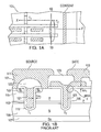
- FIGS. 1A and 1B depict one example of a conventional trench DMOS transistor 101.
- the device is provided with a first trench 103 which is in the active region of the transistor and a second trench 105 which is in the termination region of the transistor.
- FIG. 1B which is a cross-sectional view of the device of FIG. 1A taken along the line X-X', the trenches reside in a substrate comprising an n+ doped layer 107, an n doped epitaxial layer 109, and a p type diffusion layer 111 of opposite conductivity.
- An n+ doped epitaxial layer 113 which overlies the p type diffusion layer serves as the source.
- the bottom of the trenches terminate in the n doped epitaxial layer.
- An insulating layer of silicon oxide 115 extends over the surface of both trenches.
- a source electrode 117 extends over the first trench, and a gate electrode 119 extends over the second trench. Both trenches are filled with polysilicon 121 and capped with BPSG 123 (boron phosphorosilicate glass).
- Devices of this type have at least one drawback that is an artifact of the methodology by which the device is manufactured.
- the device is typically subjected to at least two oxidation treatments during its manufacture, the first of which is employed for the removal of damages occurring at the time of silicon etching after formation of the trenches, and the second of which is used to form the silicon oxide layer. As shown in FIG.
- these oxidation steps produce a defect 125 in the form of a protrusion of the p type diffusion layer 111 into the silicon oxide layer 115.
- This defect often referred to as a "horn", occurs in the upper end corner of the sidewall of the tench.
- the horn terminates in an acute angle.
- the thickness "t h " of the silicon oxide layer in the vicinity of the horn will be smaller than the average thickness t ox2 of the silicon oxide layer positioned on the sidewall of the trench or on the surface of the p type diffusion layer.
- the n type polycrystalline silicon layer 127 that covers the horn and silicon oxide layer functions as a gate and is supplied with a predetermined potential.
- an electric field between the n type polycrystalline silicon layer and the substrate is concentrated in the vicinity of horn. Since the thickness of the silicon oxide layer in the vicinity of the horn is thin, the breakdown voltage of the silicon oxide layer is greatly reduced in this area.
- U.S. 5,541,425 discloses yet another approach which is intended to overcome the problems associated with segments of the gate oxide layer that have been thinned by two-dimensional oxidation. There, a method is disclosed whereby the top corner of the trench is rounded with an additional heavy arsenic implant through the use of an additional mask.
- the methodologies proposed therein are not suitable for a power MOSFET because the floating arsenic portion causes early avalanche breakdown.
- the heavy doped arsenic portion induces silicon defects during subsequent oxidation processes such as sacrificial oxidation and gate oxidation.
- U.S. 5,639,676 discloses a method for making a trenched DMOS transistor using seven masking steps.
- a masking step is used to produce an insulating oxide layer in the termination region which is thicker than the gate oxide layer in the active region of the transistor.
- devices of this type are prone to reduction in breakdown voltage of the silicon oxide layer at the upper corner portion of the sidewall of the trench due to two-dimensional oxidation of the silicon oxide layer in this area.
- the present invention relates to methods for creating trench DMOS devices with enhanced gate oxide integrity and, in particular, to trench DMOS devices in which the gate oxide layer has improved breakdown voltage, and to the trench DMOS devices so made.
- the present invention relates to trench DMOS devices, and to methods for making the same.
- the trench DMOS devices comprise a first region (e.g., an n doped epitaxial layer) having a first conductivity type and a second region (e.g., a p type diffusion layer) having a second conductivity type, and have at least first and second trenches which are in communication with the first and second regions.
- a first electrically insulating layer is disposed over the surface of the first trench and has a mean thickness over the first trench of t 1 .
- a second electrically insulating layer is disposed over the surface of the second trench and has a mean thickness over the second trench of t 2 .
- the electrically insulating layers typically comprise an oxide such as silicon oxide.
- the ratio t 1 /t 2 is greater than 1, and is typically at least about 1.2.
- the trench DMOS devices made in accordance with this aspect of the invention are particularly useful in power MOSFET applications.
- the first trench may be disposed in the termination region of the transistor and the second trench may be disposed in the active region of the transistor.
- the presence of the thicker insulating layer in the termination region maintains the breakdown voltage of the insulating layer at an acceptable level, particularly in the vicinity of the upper corner of the trench where two-dimensional oxidation is most likely to produce horns or similar defects in the insulating layer.
- the thicker insulating layer improves the electric field distribution so that avalanche breakdown occurs in the active region of the transistor rather than in the termination region, thus causing breakdown voltage behavior to be more stable and predictable.
- the thicker insulating layer also improves process control and reduces substrate contamination during processing. Also, the thicker the oxide, the less crowded the electric field distributed so the oxide rupture voltage will be larger. 2. The thicker the oxide, the less the dopant can penetrate from the doped polysilicon through the oxide into the substrate region so a thicker oxide can help to reduce the substrate contamination.
- the average thickness of the insulating layer at the bottom of the second trench is also increased, without increasing the average thickness of the insulating layer in the upper portion of these trenches.
- Trench DMOS devices of these later embodiments have all of the advantages noted above. Moreover, the presence of a thicker insulating layer at the bottom of the trenches in the active region of a power MOSFET reduces penetration of dopant material through the insulating layer and into the p type diffusion layer in this area of the trench, thereby reducing punch-through.
- the present invention relates to a method for making trench DMOS devices, and to the devices so made.
- an article which comprises a first region having a first conductivity type and a second region having a second conductivity type.
- the article has first and second trenches which are in communication with the first and second regions.
- a first electrically insulating layer is then deposited over the surface of the first trench.
- the first insulating layer has a mean thickness over the first trench of t 1 .
- a second insulating layer is deposited over the surface of the second trench.
- the second insulating layer has a mean thickness over the second trench of t 2 .
- the thicknesses of the two insulating layers are such that, if k is the larger of the two layers and m is the smaller of the two layers, then k/m is greater than 1, and typically is at least about 1.2.
- the differences in thickness of the insulating layer may be achieved by depositing a first insulating layer over the first and second trench, and then depositing at least one mask (e.g., an oxide mask if the insulating layer is an oxide such as silicon oxide) over at least a portion of the first insulating layer, thereby defining a masked region and an unmasked region.
- the masked region extends over the entire surface of the first trench, and the unmasked region extends over the entire surface of the second trench.
- the masked region extends over the entire surface of the first trench and over a first portion of the surface of the second trench (e.g., the bottom), and the unmasked region extends over a second portion of the surface of the second trench. Any portion of the first insulating layer extending into the unmasked region is then removed, as by etching, and a second insulating layer having an average thickness t 2 , wherein t1 ⁇ t 2 , is deposited over the unmasked region. Typically, if the first trench is located in the termination region of the transistor and the second trench is located in the active region of the transistor, then t 1 > t 2 . This method may be used advantageously to produce a trench DMOS device of the type described above.
- the present invention relates to an intermediary article which is useful in the construction of a trench DMOS transistors and similar devices, and to methods for making the same.
- the article comprises a first region having a first conductivity type and a second region having a second conductivity type.
- a first trench which is in communication with the first and second regions, has first and second walls and terminates in a first bottom.
- the first wall extends from the first bottom to a surface of the article, and the intersection of the first wall and the surface defines a first locus.
- a second trench which has third and fourth walls and terminate in a second bottom (the second bottom defines a second locus), also extends through the first and second regions.
- An electrically insulating material (typically an insulating oxide such as silicon oxide) is disposed over at least the first locus.
- the insulating material extends over the second locus as well.
- the article is further provided with at least one mask which defines a masked region and an unmasked region.
- the masked region extends over the first locus and, in some embodiments, extends over the second locus as well.
- the unmasked region extends over all areas outside of the masked region, and typically includes at least a portion of the third and fourth walls of the second trench.
- the intermediary articles of the present invention may be used advantageously in the manufacture of the trench DMOS transistors and devices of the present invention, as by removing any insulating material present in the unmasked region (as, for example, by chemical etching, where the insulating material is silicon oxide and the at least one mask is an oxide mask) and then depositing another portion of the same or different insulating material over the unmasked region (either before or after removal of the at least one mask).
- the thickness of the insulating material (which may form the gate oxide layer and/or a sacrificial oxide layer) may be varied independently over the masked and unmasked regions of the trench DMOS device so as to obtain the benefits described above.
- FIG. 1A is a plan view of a prior art DMOS device
- FIG. 1B is a cross-sectional view taken along the Line 1B-1B of FIG. 1 ;
- FIG. 1C is a magnified view of Area 2 in FIG. 2 ;
- FIGS. 2-5 are a schematic cross-sectional views of trench DMOS transistor constructed in accordance with the present invention.
- FIGS. 6A-6E are schematic cross-sectional views illustrating a method of making trench DMOS transistors in accordance with the present invention.
- FIGS. 7A-7D are schematic cross-sectional views illustrating a method of making trench DMOS transistors in accordance with the present invention.
- FIGS. 8A-8B are schematic cross-sectional views illustrating a method of making trench DMOS transistors in accordance with the present invention.
- the present invention pertains to trench DMOS devices (and to methods for making the same) with improved gate oxide integrity and, in particular, to trench DMOS devices having a gate oxide layer with improved breakdown voltage. These devices, and the methodology for making them, are particularly useful in making power MOSFET devices.
- FIG. 2 illustrates a first embodiment of a trench DMOS device 1 which is made in accordance with the present invention.
- the structure includes an n+ substrate 3 on which is grown a lightly n doped epitaxial layer 5 .
- a p type diffusion layer 7 of opposite conductivity is provided within the doped epitaxial layer.
- An N+ doped epitaxial layer 9 that overlies at least a portion of the p type diffusion layer serves as the source.
- First and second trenches 11,11 ' are provided in the epitaxial layer.
- the first trench is disposed in the active region 12 of the device and the second trench is disposed in the termination region 12 ' of the device.
- the second trench is filled with a portion of polysilicon which 14 extends to the top surface for contact with the gate 16 .
- First and second oxide layers 13,13 ' are provided in first and second trenches, respectively, the first and second oxide layers having respective thicknesses of t 1 and t 2 such that t 2 > t 1 .
- the thicknesses t 1 and t 2 are chosen such that the breakdown voltage of the oxide layers are sufficient for the intended end use, subject to the requirement that t 2 > t 1 .
- the presence of the thicker oxide layer in the termination region maintains the breakdown voltage of the oxide layer at an acceptable level in the vicinity of the upper corner of the trench, where two-dimensional oxidation is most likely to produce horns or similar defects.
- the thicker oxide layer improves the electric field distribution so that avalanche breakdown occurs in the active region of the transistor rather than in the termination region, thus causing breakdown voltage behavior to be more stable and predictable.
- the thicker silicon oxide layer also improves process control and reduces substrate contamination during processing.
- t 1 and t 2 will be chosen such that the ratio t 2 :t 1l is at least about 1.2, more preferably at least about 1.5, and most preferably at least about 2.
- t 1 is within the range of 400 to 700 angstroms, more preferably within the range of 500 to 650 angstroms, and most preferably within the range of 550 to 600 angstroms
- t 2 is typically within the range of 600 to 840 angstroms, more preferably within the range of 750 to 1050 angstroms, and most preferably within the range of 1000 to 1400 angstroms.
- the gate oxide thickness i.e., the oxide in the trench located in the active area depends on the voltage of the device being fabricated.
- FIG. 3 illustrates a second embodiment of a trench DMOS structure 21 which is made in accordance with the present invention.
- This structure is similar to that depicted in FIG. 2 , except that masking techniques are used to thicken the portion of the gate oxide layer 23 along the bottom of the first trench 25 as compared to the device of FIG. 2 .
- This thickening of the gate oxide layer is advantageous in that it reduces penetration of dopant material through the insulating layer and into the p type diffusion layer in this area of the trench, thereby reducing punch-through.
- the gate oxide layer is thinner elsewhere in the trench, thereby ensuring that avalanche breakdown occurs in the active region of the transistor rather than in the termination region.
- Typical values for the thickness t b of the oxide layer at the bottom of the first trench, and the thickness t s of the oxide layer along the sides of the trench, are comparable to the values of t 1 and t 2 , respectively, for the device depicted in FIG. 2 .
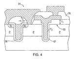
- FIG. 4 illustrates a third embodiment of a trench DMOS structure 31 which is made in accordance with the present invention.
- This device is similar to the device depicted in FIG. 3 , except that additional masking steps are used to produce an insulating oxide layer 33 in the termination region of the device which has a first region 35 with a thickness t 1 and a second region 37 with a thickness t 2 .
- the gate oxide layer 38 in the active region of the device has a thickness t 3 .
- the thicknesses of these layers are chosen such that t 1 > t 2 > t 3 .
- t 1 and t 2 will be chosen such that the ratio t 1 :t 2 is at least about 1.5, more preferably at least about 3.0, and most preferably at least about 4.0.
- t 1 is within the range of 1500 to 2000 angstroms, more preferably within the range of 2000 to 2500 angstroms, and most preferably within the range of 3500 to 4500 angstroms
- t 2 is typically within the range of 600 to 840 angstroms, more preferably within the range of 750 to 1050 angstroms, and most preferably within the range of 1000 to 1400 angstroms.
- Typical values for t 3 correspond to the values for t 2 in the device of FIG. 2 .
- the additional thickness of the first region in this embodiment is advantageous in that it reduces the Gate runner capacitance.
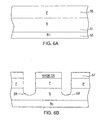
- FIG. 5 illustrates a fourth embodiment of a trench DMOS structure 41 which is made in accordance with the present invention.
- This device is similar to the device depicted in FIG. 4 except that masking techniques are used to thicken the portion 43 of the gate oxide layer 45 along the bottom of the trench 47 in the active region of the device.
- the benefits of a thicker oxide layer in this region have been noted with respect to the embodiment depicted in FIG. 3 .
- Portion 43 of the gate oxide layer will typically have a thickness t 4 comparable to the values of t 2 in the device depicted in FIG. 4 .
- FIG. 6A-6E illustrate a first embodiment of the method of the present invention that may be used to form a trench DMOS device of the type depicted in FIG. 4 .
- an n doped epitaxial layer 51 is grown on a conventionally n+ doped substrate 53.
- the epitaxial layer is typically 5.5 microns in thickness for a 30 V device.
- p type diffusion layer 55 is formed in an implantation and diffusion step. Since the p type diffusion layer is uniform across the substrate, no mask is needed.
- the p type diffusion layer may be boron implanted at 40 to 60 KEV with a dosage of 5.5 x 10 13 /cm 3 .
- a mask oxide layer is formed by covering the surface of the epitaxial layer with an oxide layer, which is then conventionally exposed and patterned to leave mask portions 57.
- Mask portions 57 are used for defining the location of the first and second trenches 59, 59 ' which are dry etched through the mask openings by reactive ion etching to a depth that typically ranges from 1.5 to 2.5 microns.
- the mask portions are removed, typically by a buffer oxide etch or an HF etch. Since the steps of trench formation are completed prior to removal of the patterned trench mask, and since the patterned trench mask serves as a cap or buffer during the trench forming process, dopant material does not leach out of the p type diffusion layer, and punch-through is consequently reduced.
- a sacrificial oxide layer 61 is deposited on the entire structure so that it covers the trench walls and the surface of p type diffusion layer 55.
- the sacrificial oxide layer typically has a thickness t 2 in the range of 800 angstroms, more preferably within the range of 1000 angstroms, and most preferably within the range of 1200 angstroms.
- a sacrificial oxide mask 71 is deposited over the second trench 59', while the first trench 59 is left exposed.
- the sacrificial oxide layer is then removed from the surface of the first trench by means of an oxide etch.
- gate oxide layer 75 is then deposited on the surface of the first trench, followed by polysilicon 77 deposition.
- the polysilicon is then doped with phosphorous chloride or implanted with arsenic or phosphorous to reduce its resistivity, which resistivity is typically within the range of 20 ohm per square cm.
- a photoresist polysilicon mask 79 is then placed over the second trench, and the device is completed in a conventional manner to produce a device such as that depicted in FIG. 2 .
- FIGS. 7A-7B show a second embodiment of the method of the present invention.
- first and second sacrificial oxide masks 81, 81' are deposited over the structure depicted in FIG. 6C such that the sacrificial oxide layer 82, which has an average thickness t 1 , is completely covered in the vicinity of the second trench 83' but is covered only at the bottom of the first trench 83.
- the resulting structure is then exposed to an oxide etch which removes a portion of the sacrificial oxide layer in the vicinity of the first trench as shown in FIG. 7B .
- the sacrificial oxide masks are then removed and a gate oxide layer 85 having an average thickness t 2 is deposited to give the structure depicted in FIG. 7C .
- a layer of polysilicon 87 is then deposited over the gate oxide layer and sacrificial oxide layer, the polysilicon is doped, and a photoresist polysilicon mask 89 is placed over the second trench to give the structure depicted in FIG. 7D .
- the device is then completed in a conventional manner to result in a device such as that depicted in FIG. 3 . Typical values for t 1 and t 2 are noted with respect to the device depicted in FIG. 3 .
- FIGS. 8A-8B show a third embodiment of the method of the present invention.
- a first oxide layer 91 having a thickness t 1 is deposited over a substrate of the type depicted in FIG. 6A .
- the first oxide layer is then patterned into a prescribed shape having at least first and second openings 93, 93', thereby forming an oxide mask.
- Corresponding first and second trenches 95, 95' are then anisotropically etched through the mask openings.
- a sacrificial oxide layer (not shown) is deposited over the etched structure to remove any damages that occurred during etching, after which the sacrificial oxide layer is removed.
- the trenches are subject to thermal oxidation to form a second oxide film 97 having a thickness t 2 , wherein t 1 > t 2 , over the surfaces of the trenches.
- a second oxide film 97 having a thickness t 2 , wherein t 1 > t 2 , over the surfaces of the trenches.
- Such a film may be formed, for example, in an oxygen/hydrogen atmosphere at about 950°C, with the time of deposition and other parameters being controlled to achieve a desired layer thickness.
- An oxide mask 99 is then deposited over the second trench.
- the device is then typically subjected to an oxide etch to form a structure analogous to that shown in FIG. 6D , and is completed using methodology similar to that described with respect to FIG. 6E to result in the device depicted in FIG. 4 .
- additional masking steps e.g., the placement of an oxide mask on the bottom of the first trench
- oxide etching may be performed prior to oxide etching so as to form a device such as that depicted in FIG. 5 in which the gate oxide layer is thickened in the vicinity of the bottom of the first trench.
- the method of the present invention may be used to form a trench DMOS in which the conductivities of the various semiconductor regions are reversed from those described herein.
Landscapes
- Insulated Gate Type Field-Effect Transistor (AREA)
- Electrodes Of Semiconductors (AREA)
- Formation Of Insulating Films (AREA)
- Metal-Oxide And Bipolar Metal-Oxide Semiconductor Integrated Circuits (AREA)
Applications Claiming Priority (3)
| Application Number | Priority Date | Filing Date | Title |
|---|---|---|---|
| US59512000A | 2000-06-16 | 2000-06-16 | |
| EP01948426A EP1295343A2 (fr) | 2000-06-16 | 2001-06-15 | Dispositif a tranchee pour semi-conducteur comprenant une structure ayant une meilleure integrite de l'oxyde de la grille |
| PCT/US2001/019377 WO2001099198A2 (fr) | 2000-06-16 | 2001-06-15 | Dispositif a tranchee pour semi-conducteur comprenant une structure ayant une meilleure integrite de l'oxyde de la grille |
Related Parent Applications (2)
| Application Number | Title | Priority Date | Filing Date |
|---|---|---|---|
| EP01948426.0 Division | 2001-06-15 | ||
| EP01948426A Division EP1295343A2 (fr) | 2000-06-16 | 2001-06-15 | Dispositif a tranchee pour semi-conducteur comprenant une structure ayant une meilleure integrite de l'oxyde de la grille |
Publications (3)
| Publication Number | Publication Date |
|---|---|
| EP2267787A2 true EP2267787A2 (fr) | 2010-12-29 |
| EP2267787A3 EP2267787A3 (fr) | 2011-01-12 |
| EP2267787B1 EP2267787B1 (fr) | 2020-04-22 |
Family
ID=24381814
Family Applications (2)
| Application Number | Title | Priority Date | Filing Date |
|---|---|---|---|
| EP10012844.6A Expired - Lifetime EP2267787B1 (fr) | 2000-06-16 | 2001-06-15 | Méthode de fabrication d'un transistor à effet de champ DMOS à grille en tranchée |
| EP01948426A Ceased EP1295343A2 (fr) | 2000-06-16 | 2001-06-15 | Dispositif a tranchee pour semi-conducteur comprenant une structure ayant une meilleure integrite de l'oxyde de la grille |
Family Applications After (1)
| Application Number | Title | Priority Date | Filing Date |
|---|---|---|---|
| EP01948426A Ceased EP1295343A2 (fr) | 2000-06-16 | 2001-06-15 | Dispositif a tranchee pour semi-conducteur comprenant une structure ayant une meilleure integrite de l'oxyde de la grille |
Country Status (8)
| Country | Link |
|---|---|
| US (1) | US6620691B2 (fr) |
| EP (2) | EP2267787B1 (fr) |
| JP (1) | JP5442921B2 (fr) |
| KR (1) | KR100850689B1 (fr) |
| CN (1) | CN100416855C (fr) |
| AU (1) | AU2001269878A1 (fr) |
| TW (1) | TW523816B (fr) |
| WO (1) | WO2001099198A2 (fr) |
Families Citing this family (23)
| Publication number | Priority date | Publication date | Assignee | Title |
|---|---|---|---|---|
| JP4860102B2 (ja) * | 2003-06-26 | 2012-01-25 | ルネサスエレクトロニクス株式会社 | 半導体装置 |
| TWI400757B (zh) * | 2005-06-29 | 2013-07-01 | 快捷半導體公司 | 形成遮蔽閘極場效應電晶體之方法 |
| KR100905778B1 (ko) | 2006-12-29 | 2009-07-02 | 주식회사 하이닉스반도체 | 반도체 소자의 제조 방법 |
| JP4600936B2 (ja) | 2007-06-20 | 2010-12-22 | 三菱電機株式会社 | 半導体装置およびその製造方法 |
| JP5123622B2 (ja) * | 2007-09-13 | 2013-01-23 | 株式会社日立製作所 | 半導体装置及びその製造方法 |
| US9484451B2 (en) | 2007-10-05 | 2016-11-01 | Vishay-Siliconix | MOSFET active area and edge termination area charge balance |
| US8314471B2 (en) * | 2009-11-17 | 2012-11-20 | Diodes Incorporated | Trench devices having improved breakdown voltages and method for manufacturing same |
| US8698232B2 (en) | 2010-01-04 | 2014-04-15 | International Rectifier Corporation | Semiconductor device including a voltage controlled termination structure and method for fabricating same |
| TWI438901B (zh) | 2010-05-27 | 2014-05-21 | Sinopower Semiconductor Inc | 具有低閘極輸入電阻之功率半導體元件及其製作方法 |
| US9431249B2 (en) | 2011-12-01 | 2016-08-30 | Vishay-Siliconix | Edge termination for super junction MOSFET devices |
| US9614043B2 (en) * | 2012-02-09 | 2017-04-04 | Vishay-Siliconix | MOSFET termination trench |
| US9842911B2 (en) | 2012-05-30 | 2017-12-12 | Vishay-Siliconix | Adaptive charge balanced edge termination |
| TW201423869A (zh) * | 2012-12-13 | 2014-06-16 | 茂達電子股份有限公司 | 溝渠式電晶體的製作方法 |
| DE102013108518B4 (de) * | 2013-08-07 | 2016-11-24 | Infineon Technologies Ag | Halbleitervorrichtung und verfahren zum herstellen derselben |
| US9023709B2 (en) * | 2013-08-27 | 2015-05-05 | Globalfoundries Inc. | Top corner rounding by implant-enhanced wet etching |
| JP6168961B2 (ja) * | 2013-10-10 | 2017-07-26 | 三菱電機株式会社 | 半導体装置 |
| US10395970B2 (en) * | 2013-12-05 | 2019-08-27 | Vishay-Siliconix | Dual trench structure |
| JP2015230932A (ja) * | 2014-06-04 | 2015-12-21 | 三菱電機株式会社 | 炭化珪素半導体装置および炭化珪素半導体装置の製造方法 |
| US9887259B2 (en) | 2014-06-23 | 2018-02-06 | Vishay-Siliconix | Modulated super junction power MOSFET devices |
| KR102098996B1 (ko) | 2014-08-19 | 2020-04-08 | 비쉐이-실리코닉스 | 초접합 금속 산화물 반도체 전계 효과 트랜지스터 |
| CN104167354B (zh) * | 2014-09-18 | 2017-07-28 | 上海华力微电子有限公司 | 通过栅氧的双氧化提高栅氧均匀性的方法 |
| US9673314B2 (en) | 2015-07-08 | 2017-06-06 | Vishay-Siliconix | Semiconductor device with non-uniform trench oxide layer |
| CN105185698A (zh) * | 2015-08-11 | 2015-12-23 | 上海华虹宏力半导体制造有限公司 | 减少沟道功率器件的源漏击穿电压蠕变的方法 |
Citations (9)
| Publication number | Priority date | Publication date | Assignee | Title |
|---|---|---|---|---|
| JPS63166230A (ja) | 1986-12-26 | 1988-07-09 | Toshiba Corp | ドライエツチング方法 |
| JPS6457623A (en) | 1987-08-28 | 1989-03-03 | Toshiba Corp | Manufacture of semiconductor device |
| US5072266A (en) | 1988-12-27 | 1991-12-10 | Siliconix Incorporated | Trench DMOS power transistor with field-shaping body profile and three-dimensional geometry |
| US5304381A (en) | 1989-03-17 | 1994-04-19 | Eisai Co., Ltd. | Stabilization of polyprenyl compound |
| US5316959A (en) | 1992-08-12 | 1994-05-31 | Siliconix, Incorporated | Trenched DMOS transistor fabrication using six masks |
| US5430324A (en) | 1992-07-23 | 1995-07-04 | Siliconix, Incorporated | High voltage transistor having edge termination utilizing trench technology |
| US5541425A (en) | 1994-01-20 | 1996-07-30 | Mitsubishi Denki Kabushiki Kaisha | Semiconductor device having trench structure |
| US5639676A (en) | 1994-08-15 | 1997-06-17 | Siliconix Incorporated | Trenched DMOS transistor fabrication having thick termination region oxide |
| US5866931A (en) | 1993-04-14 | 1999-02-02 | Siliconix Incorporated | DMOS power transistor with reduced number of contacts using integrated body-source connections |
Family Cites Families (16)
| Publication number | Priority date | Publication date | Assignee | Title |
|---|---|---|---|---|
| JP2573272B2 (ja) | 1987-06-15 | 1997-01-22 | 株式会社東芝 | 半導体記憶装置 |
| JP2644515B2 (ja) * | 1988-01-27 | 1997-08-25 | 株式会社日立製作所 | 半導体装置 |
| US5304831A (en) | 1990-12-21 | 1994-04-19 | Siliconix Incorporated | Low on-resistance power MOS technology |
| JP2635828B2 (ja) * | 1991-01-09 | 1997-07-30 | 株式会社東芝 | 半導体装置 |
| US5233215A (en) * | 1992-06-08 | 1993-08-03 | North Carolina State University At Raleigh | Silicon carbide power MOSFET with floating field ring and floating field plate |
| US5468982A (en) * | 1994-06-03 | 1995-11-21 | Siliconix Incorporated | Trenched DMOS transistor with channel block at cell trench corners |
| JP3155894B2 (ja) * | 1994-09-29 | 2001-04-16 | 株式会社東芝 | 半導体装置およびその製造方法 |
| KR100373581B1 (ko) * | 1995-05-01 | 2003-05-09 | 내셔널 세미콘덕터 코포레이션 | 자기정렬된접점트렌치dmos트랜지스터를제조하는방법 |
| DE19617646C2 (de) | 1996-05-02 | 1998-07-09 | Siemens Ag | Speicherzellenanordnung und ein Verfahren zu deren Herstellung |
| JPH1098188A (ja) | 1996-08-01 | 1998-04-14 | Kansai Electric Power Co Inc:The | 絶縁ゲート半導体装置 |
| JP3924829B2 (ja) * | 1997-01-13 | 2007-06-06 | 株式会社日立製作所 | 電圧駆動型半導体装置及びその製造方法 |
| US6009023A (en) | 1998-05-26 | 1999-12-28 | Etron Technology, Inc. | High performance DRAM structure employing multiple thickness gate oxide |
| US6319759B1 (en) | 1998-08-10 | 2001-11-20 | International Business Machines Corporation | Method for making oxide |
| US5998833A (en) * | 1998-10-26 | 1999-12-07 | North Carolina State University | Power semiconductor devices having improved high frequency switching and breakdown characteristics |
| TW400615B (en) | 1998-11-23 | 2000-08-01 | United Microelectronics Corp | The structure process of Shallow Trench Isolation(STI) |
| DE19935442C1 (de) * | 1999-07-28 | 2000-12-21 | Siemens Ag | Verfahren zum Herstellen eines Trench-MOS-Leistungstransistors |
-
2001
- 2001-06-14 TW TW090114465A patent/TW523816B/zh not_active IP Right Cessation
- 2001-06-15 JP JP2002503949A patent/JP5442921B2/ja not_active Expired - Fee Related
- 2001-06-15 KR KR1020027017138A patent/KR100850689B1/ko not_active Expired - Lifetime
- 2001-06-15 WO PCT/US2001/019377 patent/WO2001099198A2/fr not_active Ceased
- 2001-06-15 CN CNB018111890A patent/CN100416855C/zh not_active Expired - Fee Related
- 2001-06-15 EP EP10012844.6A patent/EP2267787B1/fr not_active Expired - Lifetime
- 2001-06-15 EP EP01948426A patent/EP1295343A2/fr not_active Ceased
- 2001-06-15 AU AU2001269878A patent/AU2001269878A1/en not_active Abandoned
- 2001-11-20 US US10/042,558 patent/US6620691B2/en not_active Expired - Lifetime
Patent Citations (9)
| Publication number | Priority date | Publication date | Assignee | Title |
|---|---|---|---|---|
| JPS63166230A (ja) | 1986-12-26 | 1988-07-09 | Toshiba Corp | ドライエツチング方法 |
| JPS6457623A (en) | 1987-08-28 | 1989-03-03 | Toshiba Corp | Manufacture of semiconductor device |
| US5072266A (en) | 1988-12-27 | 1991-12-10 | Siliconix Incorporated | Trench DMOS power transistor with field-shaping body profile and three-dimensional geometry |
| US5304381A (en) | 1989-03-17 | 1994-04-19 | Eisai Co., Ltd. | Stabilization of polyprenyl compound |
| US5430324A (en) | 1992-07-23 | 1995-07-04 | Siliconix, Incorporated | High voltage transistor having edge termination utilizing trench technology |
| US5316959A (en) | 1992-08-12 | 1994-05-31 | Siliconix, Incorporated | Trenched DMOS transistor fabrication using six masks |
| US5866931A (en) | 1993-04-14 | 1999-02-02 | Siliconix Incorporated | DMOS power transistor with reduced number of contacts using integrated body-source connections |
| US5541425A (en) | 1994-01-20 | 1996-07-30 | Mitsubishi Denki Kabushiki Kaisha | Semiconductor device having trench structure |
| US5639676A (en) | 1994-08-15 | 1997-06-17 | Siliconix Incorporated | Trenched DMOS transistor fabrication having thick termination region oxide |
Non-Patent Citations (1)
| Title |
|---|
| IEEE TRANSACTIONS ON ELECTRON DEVICES, vol. ED-34, no. 8, August 1987 (1987-08-01), pages 1681 - 1687 |
Also Published As
| Publication number | Publication date |
|---|---|
| CN1449587A (zh) | 2003-10-15 |
| KR100850689B1 (ko) | 2008-08-07 |
| JP2004507882A (ja) | 2004-03-11 |
| AU2001269878A1 (en) | 2002-01-02 |
| CN100416855C (zh) | 2008-09-03 |
| EP1295343A2 (fr) | 2003-03-26 |
| US20020061623A1 (en) | 2002-05-23 |
| EP2267787A3 (fr) | 2011-01-12 |
| WO2001099198A3 (fr) | 2002-10-10 |
| EP2267787B1 (fr) | 2020-04-22 |
| TW523816B (en) | 2003-03-11 |
| WO2001099198A2 (fr) | 2001-12-27 |
| US6620691B2 (en) | 2003-09-16 |
| JP5442921B2 (ja) | 2014-03-19 |
| KR20030084563A (ko) | 2003-11-01 |
Similar Documents
| Publication | Publication Date | Title |
|---|---|---|
| EP2267787B1 (fr) | Méthode de fabrication d'un transistor à effet de champ DMOS à grille en tranchée | |
| EP1393362B1 (fr) | Méthode de fabrication d'un dispositif semi-conducteur à grille en tranchée | |
| US6368921B1 (en) | Manufacture of trench-gate semiconductor devices | |
| US6498071B2 (en) | Manufacture of trench-gate semiconductor devices | |
| US6545315B2 (en) | Trench DMOS transistor having reduced punch-through | |
| JP2002299619A (ja) | 半導体装置およびその製造方法 | |
| EP1386352B1 (fr) | Dispositifs semi-conducteurs à grille en tranchée et leur procédé de fabrication | |
| JP2004504711A (ja) | 高速トレンチ二重拡散金属酸化膜半導体 | |
| US6620669B2 (en) | Manufacture of trench-gate semiconductor devices | |
| US6087224A (en) | Manufacture of trench-gate semiconductor devices | |
| US6977203B2 (en) | Method of forming narrow trenches in semiconductor substrates | |
| EP0996970B1 (fr) | Fabrication de composants a semiconducteur a effet de champ | |
| JPS62169369A (ja) | 縦形半導体装置の製造方法 |
Legal Events
| Date | Code | Title | Description |
|---|---|---|---|
| PUAI | Public reference made under article 153(3) epc to a published international application that has entered the european phase |
Free format text: ORIGINAL CODE: 0009012 |
|
| PUAL | Search report despatched |
Free format text: ORIGINAL CODE: 0009013 |
|
| AC | Divisional application: reference to earlier application |
Ref document number: 1295343 Country of ref document: EP Kind code of ref document: P |
|
| AK | Designated contracting states |
Kind code of ref document: A2 Designated state(s): DE FR |
|
| AK | Designated contracting states |
Kind code of ref document: A3 Designated state(s): DE FR |
|
| 17P | Request for examination filed |
Effective date: 20110712 |
|
| 17Q | First examination report despatched |
Effective date: 20130911 |
|
| GRAP | Despatch of communication of intention to grant a patent |
Free format text: ORIGINAL CODE: EPIDOSNIGR1 |
|
| RIC1 | Information provided on ipc code assigned before grant |
Ipc: H01L 29/423 20060101ALI20191010BHEP Ipc: H01L 29/78 20060101AFI20191010BHEP Ipc: H01L 21/336 20060101ALI20191010BHEP |
|
| INTG | Intention to grant announced |
Effective date: 20191108 |
|
| RAP1 | Party data changed (applicant data changed or rights of an application transferred) |
Owner name: GENERAL SEMICONDUCTOR, INC. |
|
| GRAS | Grant fee paid |
Free format text: ORIGINAL CODE: EPIDOSNIGR3 |
|
| GRAA | (expected) grant |
Free format text: ORIGINAL CODE: 0009210 |
|
| STAA | Information on the status of an ep patent application or granted ep patent |
Free format text: STATUS: THE PATENT HAS BEEN GRANTED |
|
| AC | Divisional application: reference to earlier application |
Ref document number: 1295343 Country of ref document: EP Kind code of ref document: P |
|
| AK | Designated contracting states |
Kind code of ref document: B1 Designated state(s): DE FR |
|
| REG | Reference to a national code |
Ref country code: DE Ref legal event code: R096 Ref document number: 60151270 Country of ref document: DE |
|
| PGFP | Annual fee paid to national office [announced via postgrant information from national office to epo] |
Ref country code: FR Payment date: 20200625 Year of fee payment: 20 Ref country code: DE Payment date: 20200629 Year of fee payment: 20 |
|
| REG | Reference to a national code |
Ref country code: DE Ref legal event code: R097 Ref document number: 60151270 Country of ref document: DE |
|
| PLBE | No opposition filed within time limit |
Free format text: ORIGINAL CODE: 0009261 |
|
| STAA | Information on the status of an ep patent application or granted ep patent |
Free format text: STATUS: NO OPPOSITION FILED WITHIN TIME LIMIT |
|
| 26N | No opposition filed |
Effective date: 20210125 |
|
| REG | Reference to a national code |
Ref country code: DE Ref legal event code: R071 Ref document number: 60151270 Country of ref document: DE |