EP2472625B1 - Organische Halbleiterverbindungen mit geringen Bandabständen sowie elektronische Vorrichtungen damit - Google Patents
Organische Halbleiterverbindungen mit geringen Bandabständen sowie elektronische Vorrichtungen damit Download PDFInfo
- Publication number
- EP2472625B1 EP2472625B1 EP12150078.9A EP12150078A EP2472625B1 EP 2472625 B1 EP2472625 B1 EP 2472625B1 EP 12150078 A EP12150078 A EP 12150078A EP 2472625 B1 EP2472625 B1 EP 2472625B1
- Authority
- EP
- European Patent Office
- Prior art keywords
- substituted
- unsubstituted
- group
- chemical formula
- organic semiconductor
- Prior art date
- Legal status (The legal status is an assumption and is not a legal conclusion. Google has not performed a legal analysis and makes no representation as to the accuracy of the status listed.)
- Not-in-force
Links
- 0 CCC(CC1*CC1)C=C(C)C(***1)[C@@]1C(C)=CC Chemical compound CCC(CC1*CC1)C=C(C)C(***1)[C@@]1C(C)=CC 0.000 description 6
- XBXQXYFAXLGVNM-UHFFFAOYSA-N COc1cccc(-c(c(-c2cccc(OC)c2)nc2c(nc3)Br)nc2c3Br)c1 Chemical compound COc1cccc(-c(c(-c2cccc(OC)c2)nc2c(nc3)Br)nc2c3Br)c1 XBXQXYFAXLGVNM-UHFFFAOYSA-N 0.000 description 1
Images



Classifications
-
- C—CHEMISTRY; METALLURGY
- C07—ORGANIC CHEMISTRY
- C07D—HETEROCYCLIC COMPOUNDS
- C07D495/00—Heterocyclic compounds containing in the condensed system at least one hetero ring having sulfur atoms as the only ring hetero atoms
- C07D495/02—Heterocyclic compounds containing in the condensed system at least one hetero ring having sulfur atoms as the only ring hetero atoms in which the condensed system contains two hetero rings
- C07D495/04—Ortho-condensed systems
-
- B—PERFORMING OPERATIONS; TRANSPORTING
- B82—NANOTECHNOLOGY
- B82Y—SPECIFIC USES OR APPLICATIONS OF NANOSTRUCTURES; MEASUREMENT OR ANALYSIS OF NANOSTRUCTURES; MANUFACTURE OR TREATMENT OF NANOSTRUCTURES
- B82Y10/00—Nanotechnology for information processing, storage or transmission, e.g. quantum computing or single electron logic
-
- C—CHEMISTRY; METALLURGY
- C07—ORGANIC CHEMISTRY
- C07D—HETEROCYCLIC COMPOUNDS
- C07D471/00—Heterocyclic compounds containing nitrogen atoms as the only ring hetero atoms in the condensed system, at least one ring being a six-membered ring with one nitrogen atom, not provided for by groups C07D451/00 - C07D463/00
- C07D471/02—Heterocyclic compounds containing nitrogen atoms as the only ring hetero atoms in the condensed system, at least one ring being a six-membered ring with one nitrogen atom, not provided for by groups C07D451/00 - C07D463/00 in which the condensed system contains two hetero rings
- C07D471/04—Ortho-condensed systems
-
- C—CHEMISTRY; METALLURGY
- C08—ORGANIC MACROMOLECULAR COMPOUNDS; THEIR PREPARATION OR CHEMICAL WORKING-UP; COMPOSITIONS BASED THEREON
- C08G—MACROMOLECULAR COMPOUNDS OBTAINED OTHERWISE THAN BY REACTIONS ONLY INVOLVING UNSATURATED CARBON-TO-CARBON BONDS
- C08G61/00—Macromolecular compounds obtained by reactions forming a carbon-to-carbon link in the main chain of the macromolecule
- C08G61/12—Macromolecular compounds containing atoms other than carbon in the main chain of the macromolecule
- C08G61/122—Macromolecular compounds containing atoms other than carbon in the main chain of the macromolecule derived from five- or six-membered heterocyclic compounds, other than imides
-
- C—CHEMISTRY; METALLURGY
- C08—ORGANIC MACROMOLECULAR COMPOUNDS; THEIR PREPARATION OR CHEMICAL WORKING-UP; COMPOSITIONS BASED THEREON
- C08G—MACROMOLECULAR COMPOUNDS OBTAINED OTHERWISE THAN BY REACTIONS ONLY INVOLVING UNSATURATED CARBON-TO-CARBON BONDS
- C08G61/00—Macromolecular compounds obtained by reactions forming a carbon-to-carbon link in the main chain of the macromolecule
- C08G61/12—Macromolecular compounds containing atoms other than carbon in the main chain of the macromolecule
- C08G61/122—Macromolecular compounds containing atoms other than carbon in the main chain of the macromolecule derived from five- or six-membered heterocyclic compounds, other than imides
- C08G61/123—Macromolecular compounds containing atoms other than carbon in the main chain of the macromolecule derived from five- or six-membered heterocyclic compounds, other than imides derived from five-membered heterocyclic compounds
-
- C—CHEMISTRY; METALLURGY
- C09—DYES; PAINTS; POLISHES; NATURAL RESINS; ADHESIVES; COMPOSITIONS NOT OTHERWISE PROVIDED FOR; APPLICATIONS OF MATERIALS NOT OTHERWISE PROVIDED FOR
- C09B—ORGANIC DYES OR CLOSELY-RELATED COMPOUNDS FOR PRODUCING DYES, e.g. PIGMENTS; MORDANTS; LAKES
- C09B69/00—Dyes not provided for by a single group of this subclass
- C09B69/10—Polymeric dyes; Reaction products of dyes with monomers or with macromolecular compounds
- C09B69/109—Polymeric dyes; Reaction products of dyes with monomers or with macromolecular compounds containing other specific dyes
-
- H—ELECTRICITY
- H10—SEMICONDUCTOR DEVICES; ELECTRIC SOLID-STATE DEVICES NOT OTHERWISE PROVIDED FOR
- H10K—ORGANIC ELECTRIC SOLID-STATE DEVICES
- H10K10/00—Organic devices specially adapted for rectifying, amplifying, oscillating or switching; Organic capacitors or resistors having potential barriers
- H10K10/40—Organic transistors
- H10K10/46—Field-effect transistors, e.g. organic thin-film transistors [OTFT]
- H10K10/462—Insulated gate field-effect transistors [IGFETs]
- H10K10/484—Insulated gate field-effect transistors [IGFETs] characterised by the channel regions
-
- H—ELECTRICITY
- H10—SEMICONDUCTOR DEVICES; ELECTRIC SOLID-STATE DEVICES NOT OTHERWISE PROVIDED FOR
- H10K—ORGANIC ELECTRIC SOLID-STATE DEVICES
- H10K30/00—Organic devices sensitive to infrared radiation, light, electromagnetic radiation of shorter wavelength or corpuscular radiation
- H10K30/30—Organic devices sensitive to infrared radiation, light, electromagnetic radiation of shorter wavelength or corpuscular radiation comprising bulk heterojunctions, e.g. interpenetrating networks of donor and acceptor material domains
-
- H—ELECTRICITY
- H10—SEMICONDUCTOR DEVICES; ELECTRIC SOLID-STATE DEVICES NOT OTHERWISE PROVIDED FOR
- H10K—ORGANIC ELECTRIC SOLID-STATE DEVICES
- H10K85/00—Organic materials used in the body or electrodes of devices covered by this subclass
- H10K85/10—Organic polymers or oligomers
- H10K85/111—Organic polymers or oligomers comprising aromatic, heteroaromatic, or aryl chains, e.g. polyaniline, polyphenylene or polyphenylene vinylene
- H10K85/113—Heteroaromatic compounds comprising sulfur or selene, e.g. polythiophene
-
- H—ELECTRICITY
- H10—SEMICONDUCTOR DEVICES; ELECTRIC SOLID-STATE DEVICES NOT OTHERWISE PROVIDED FOR
- H10K—ORGANIC ELECTRIC SOLID-STATE DEVICES
- H10K85/00—Organic materials used in the body or electrodes of devices covered by this subclass
- H10K85/10—Organic polymers or oligomers
- H10K85/151—Copolymers
-
- H—ELECTRICITY
- H10—SEMICONDUCTOR DEVICES; ELECTRIC SOLID-STATE DEVICES NOT OTHERWISE PROVIDED FOR
- H10K—ORGANIC ELECTRIC SOLID-STATE DEVICES
- H10K85/00—Organic materials used in the body or electrodes of devices covered by this subclass
- H10K85/60—Organic compounds having low molecular weight
- H10K85/649—Aromatic compounds comprising a hetero atom
- H10K85/655—Aromatic compounds comprising a hetero atom comprising only sulfur as heteroatom
-
- H—ELECTRICITY
- H10—SEMICONDUCTOR DEVICES; ELECTRIC SOLID-STATE DEVICES NOT OTHERWISE PROVIDED FOR
- H10K—ORGANIC ELECTRIC SOLID-STATE DEVICES
- H10K85/00—Organic materials used in the body or electrodes of devices covered by this subclass
- H10K85/60—Organic compounds having low molecular weight
- H10K85/649—Aromatic compounds comprising a hetero atom
- H10K85/657—Polycyclic condensed heteroaromatic hydrocarbons
- H10K85/6572—Polycyclic condensed heteroaromatic hydrocarbons comprising only nitrogen in the heteroaromatic polycondensed ring system, e.g. phenanthroline or carbazole
-
- H—ELECTRICITY
- H10—SEMICONDUCTOR DEVICES; ELECTRIC SOLID-STATE DEVICES NOT OTHERWISE PROVIDED FOR
- H10K—ORGANIC ELECTRIC SOLID-STATE DEVICES
- H10K85/00—Organic materials used in the body or electrodes of devices covered by this subclass
- H10K85/60—Organic compounds having low molecular weight
- H10K85/649—Aromatic compounds comprising a hetero atom
- H10K85/657—Polycyclic condensed heteroaromatic hydrocarbons
- H10K85/6576—Polycyclic condensed heteroaromatic hydrocarbons comprising only sulfur in the heteroaromatic polycondensed ring system, e.g. benzothiophene
-
- C—CHEMISTRY; METALLURGY
- C08—ORGANIC MACROMOLECULAR COMPOUNDS; THEIR PREPARATION OR CHEMICAL WORKING-UP; COMPOSITIONS BASED THEREON
- C08G—MACROMOLECULAR COMPOUNDS OBTAINED OTHERWISE THAN BY REACTIONS ONLY INVOLVING UNSATURATED CARBON-TO-CARBON BONDS
- C08G2261/00—Macromolecular compounds obtained by reactions forming a carbon-to-carbon link in the main chain of the macromolecule
- C08G2261/10—Definition of the polymer structure
- C08G2261/12—Copolymers
- C08G2261/124—Copolymers alternating
-
- C—CHEMISTRY; METALLURGY
- C08—ORGANIC MACROMOLECULAR COMPOUNDS; THEIR PREPARATION OR CHEMICAL WORKING-UP; COMPOSITIONS BASED THEREON
- C08G—MACROMOLECULAR COMPOUNDS OBTAINED OTHERWISE THAN BY REACTIONS ONLY INVOLVING UNSATURATED CARBON-TO-CARBON BONDS
- C08G2261/00—Macromolecular compounds obtained by reactions forming a carbon-to-carbon link in the main chain of the macromolecule
- C08G2261/30—Monomer units or repeat units incorporating structural elements in the main chain
- C08G2261/32—Monomer units or repeat units incorporating structural elements in the main chain incorporating heteroaromatic structural elements in the main chain
- C08G2261/322—Monomer units or repeat units incorporating structural elements in the main chain incorporating heteroaromatic structural elements in the main chain non-condensed
- C08G2261/3223—Monomer units or repeat units incorporating structural elements in the main chain incorporating heteroaromatic structural elements in the main chain non-condensed containing one or more sulfur atoms as the only heteroatom, e.g. thiophene
-
- C—CHEMISTRY; METALLURGY
- C08—ORGANIC MACROMOLECULAR COMPOUNDS; THEIR PREPARATION OR CHEMICAL WORKING-UP; COMPOSITIONS BASED THEREON
- C08G—MACROMOLECULAR COMPOUNDS OBTAINED OTHERWISE THAN BY REACTIONS ONLY INVOLVING UNSATURATED CARBON-TO-CARBON BONDS
- C08G2261/00—Macromolecular compounds obtained by reactions forming a carbon-to-carbon link in the main chain of the macromolecule
- C08G2261/30—Monomer units or repeat units incorporating structural elements in the main chain
- C08G2261/32—Monomer units or repeat units incorporating structural elements in the main chain incorporating heteroaromatic structural elements in the main chain
- C08G2261/324—Monomer units or repeat units incorporating structural elements in the main chain incorporating heteroaromatic structural elements in the main chain condensed
- C08G2261/3241—Monomer units or repeat units incorporating structural elements in the main chain incorporating heteroaromatic structural elements in the main chain condensed containing one or more nitrogen atoms as the only heteroatom, e.g. carbazole
-
- C—CHEMISTRY; METALLURGY
- C08—ORGANIC MACROMOLECULAR COMPOUNDS; THEIR PREPARATION OR CHEMICAL WORKING-UP; COMPOSITIONS BASED THEREON
- C08G—MACROMOLECULAR COMPOUNDS OBTAINED OTHERWISE THAN BY REACTIONS ONLY INVOLVING UNSATURATED CARBON-TO-CARBON BONDS
- C08G2261/00—Macromolecular compounds obtained by reactions forming a carbon-to-carbon link in the main chain of the macromolecule
- C08G2261/30—Monomer units or repeat units incorporating structural elements in the main chain
- C08G2261/32—Monomer units or repeat units incorporating structural elements in the main chain incorporating heteroaromatic structural elements in the main chain
- C08G2261/324—Monomer units or repeat units incorporating structural elements in the main chain incorporating heteroaromatic structural elements in the main chain condensed
- C08G2261/3243—Monomer units or repeat units incorporating structural elements in the main chain incorporating heteroaromatic structural elements in the main chain condensed containing one or more sulfur atoms as the only heteroatom, e.g. benzothiophene
-
- C—CHEMISTRY; METALLURGY
- C08—ORGANIC MACROMOLECULAR COMPOUNDS; THEIR PREPARATION OR CHEMICAL WORKING-UP; COMPOSITIONS BASED THEREON
- C08G—MACROMOLECULAR COMPOUNDS OBTAINED OTHERWISE THAN BY REACTIONS ONLY INVOLVING UNSATURATED CARBON-TO-CARBON BONDS
- C08G2261/00—Macromolecular compounds obtained by reactions forming a carbon-to-carbon link in the main chain of the macromolecule
- C08G2261/40—Polymerisation processes
- C08G2261/41—Organometallic coupling reactions
- C08G2261/414—Stille reactions
-
- C—CHEMISTRY; METALLURGY
- C08—ORGANIC MACROMOLECULAR COMPOUNDS; THEIR PREPARATION OR CHEMICAL WORKING-UP; COMPOSITIONS BASED THEREON
- C08G—MACROMOLECULAR COMPOUNDS OBTAINED OTHERWISE THAN BY REACTIONS ONLY INVOLVING UNSATURATED CARBON-TO-CARBON BONDS
- C08G2261/00—Macromolecular compounds obtained by reactions forming a carbon-to-carbon link in the main chain of the macromolecule
- C08G2261/90—Applications
- C08G2261/91—Photovoltaic applications
-
- C—CHEMISTRY; METALLURGY
- C08—ORGANIC MACROMOLECULAR COMPOUNDS; THEIR PREPARATION OR CHEMICAL WORKING-UP; COMPOSITIONS BASED THEREON
- C08G—MACROMOLECULAR COMPOUNDS OBTAINED OTHERWISE THAN BY REACTIONS ONLY INVOLVING UNSATURATED CARBON-TO-CARBON BONDS
- C08G2261/00—Macromolecular compounds obtained by reactions forming a carbon-to-carbon link in the main chain of the macromolecule
- C08G2261/90—Applications
- C08G2261/92—TFT applications
-
- H—ELECTRICITY
- H10—SEMICONDUCTOR DEVICES; ELECTRIC SOLID-STATE DEVICES NOT OTHERWISE PROVIDED FOR
- H10K—ORGANIC ELECTRIC SOLID-STATE DEVICES
- H10K30/00—Organic devices sensitive to infrared radiation, light, electromagnetic radiation of shorter wavelength or corpuscular radiation
- H10K30/50—Photovoltaic [PV] devices
-
- H—ELECTRICITY
- H10—SEMICONDUCTOR DEVICES; ELECTRIC SOLID-STATE DEVICES NOT OTHERWISE PROVIDED FOR
- H10K—ORGANIC ELECTRIC SOLID-STATE DEVICES
- H10K85/00—Organic materials used in the body or electrodes of devices covered by this subclass
- H10K85/20—Carbon compounds, e.g. carbon nanotubes or fullerenes
- H10K85/211—Fullerenes, e.g. C60
- H10K85/215—Fullerenes, e.g. C60 comprising substituents, e.g. PCBM
-
- Y—GENERAL TAGGING OF NEW TECHNOLOGICAL DEVELOPMENTS; GENERAL TAGGING OF CROSS-SECTIONAL TECHNOLOGIES SPANNING OVER SEVERAL SECTIONS OF THE IPC; TECHNICAL SUBJECTS COVERED BY FORMER USPC CROSS-REFERENCE ART COLLECTIONS [XRACs] AND DIGESTS
- Y02—TECHNOLOGIES OR APPLICATIONS FOR MITIGATION OR ADAPTATION AGAINST CLIMATE CHANGE
- Y02E—REDUCTION OF GREENHOUSE GAS [GHG] EMISSIONS, RELATED TO ENERGY GENERATION, TRANSMISSION OR DISTRIBUTION
- Y02E10/00—Energy generation through renewable energy sources
- Y02E10/50—Photovoltaic [PV] energy
- Y02E10/549—Organic PV cells
Definitions
- Example embodiments relate to low band gap organic semiconductor compounds and electronic devices including the same.
- CTR cathode ray tube
- LCD liquid crystal display
- OLED organic light emitting diode
- PDP plasma display panel
- SED surface-conduction electron-emitter display
- a thin film transistor including amorphous silicon as a semiconductor layer is widely used.
- the amorphous silicon thin film transistor is widely used because it may have good uniformity and high electrical properties in a doping state, but good insulating properties in a non-doping state.
- the deposition process may be performed at a relatively high temperature of about 300°C. Therefore, this process is difficult to apply to low-temperature substrates (e.g., polymer substrates and the like) to accomplish a flexible display.
- the organic thin film transistor generally includes a substrate, a gate electrode, an insulation layer, a source electrode, a drain electrode, and a channel region.
- the organic thin film transistor may be classified into a bottom contact (BC) type in which a channel region is formed on the source electrode and the drain electrode and a top contact (TC) type in which a metal electrode is formed beneath the channel region due to mask deposition and the like.
- the low molecular or oligomer organic semiconductor material filled in the channel region of the organic thin film transistor may include merocyanine, phthalocyanine, perylene, pentacene, C60, a thiophene oligomer, and so on.
- the low molecular or oligomer organic semiconductor material may be a thin film formed on the channel region mainly according to a vacuum process.
- an organic semiconductor polymer material has a workability advantage of large-area processing with a low cost in a solution method such as printing techniques.
- US 2006/0081839 A1 discloses an oligothiophene-arylene derivative wherein an arylene having n-type semiconductor characteristics is introduced into an oligothiophene having p-type semiconductor characteristics, thereby simultaneously exhibiting both p-type and n-type semiconductor characteristics.
- US 2008/0099758 A1 discloses an organic polymer semiconductor, which may include an aromatic ring derivative having p-type semiconductor properties and a heteroaromatic ring having n-type semiconductor properties in the main chain thereof, and which thus may exhibit both p-type transistor properties and n-type transistor properties when used in the organic active layer of an electronic device, e.g., an organic thin film transistor.
- US 2010/0307594 A1 discloses certain polymeric compounds and their use as organic semiconductors in organic and hybrid optical, optoelectronic, and/or electronic devices such as photovoltaic cells, light emitting diodes, light emitting transistors, and field effect transistors.
- At least some example embodiments may provide organic semiconductor compounds with excellent and/or improved charge mobility fabricated using a solution process.
- Other example embodiments may provide electronic devices including the organic semiconductor compounds, such as a transistor and an organic solar cell.
- an organic semiconductor compound includes at least one structural unit represented by the following Chemical Formula 1.
- R 1 is hydrogen
- R 2 is one of selected from a halogen, a substituted or unsubstituted C1-C20 linear or branched alkyl group, a substituted or unsubstituted C3-C20 cycloalkyl group, a substituted or unsubstituted linear or branched C1-C20 alkoxy group, a substituted or unsubstituted C3-C20 cycloalkyloxy group, a substituted or unsubstituted C6-C30 aryl group, a substituted or unsubstituted C6-C30 aryloxy group, a substituted or unsubstituted C2-C30 heteroaryl group, and a combination thereof, and selected from a C1-C20 alkyl group, a C1-C20 alkoxy group, and a C3-C20 cycloalkyl group
- Chemical Formula 1 p/(p+q) may range from 0.6 to 0.9
- Chemical Formula 1A a structural unit represented by the following Chemical Formula 1A may be selected from the structural units represented by the following Chemical Formula 3.
- Hydrogen in each ring of Chemical Formula 3 may be substituted with a substituent selected from a substituted or unsubstituted C1-C15 linear or branched alkyl group, a substituted or unsubstituted C3-C15 cycloalkyl group, a substituted or unsubstituted C1-C15 alkoxy group, a substituted or unsubstituted C6-C15 aryl group, a substituted or unsubstituted C2-C15 heteroaryl group, and a combination thereof.
- a -Z- structural unit may be at least one of the structural units represented by the following Chemical Formula 4.
- Q 1 and Q 2 are each S, CR 64 R 65 , NR 66 , or SiR 67 R 68 , where R 60 -R 68 are each independently selected from hydrogen, a substituted or unsubstituted C1-C15 linear or branched alkyl group, a substituted or unsubstituted C3-C15 cycloalkyl group, a substituted or unsubstituted C1-C15 alkoxy group, a substituted or unsubstituted C6-C15 aryl group, a substituted or unsubstituted C2-C15 heteroaryl group, and a combination thereof, and where hydrogen in each ring of Chemical Formula 4 may be substituted with a substituent selected from a substituted or unsubstituted C1-C15 linear or branched alkyl group, a substituted or unsubstituted C3- C15 cycloalkyl group, a substituted or unsubstituted C1-
- the organic semiconductor compound including the at least one structural unit of Chemical Formula 1 may include a structural unit represented by the following Chemical Formula 5.
- R 1 and R 2 are the same as in Chemical Formula 1
- X and Y are the same as in Chemical Formula 3
- Z is the same as in Chemical Formula 4
- Z' is at least one functional group represented by the above Chemical Formula 4, Z' being different from Z
- p, q, and r denote a mole ratio of each structural unit, and r/(p+q+r) is in a range of 0.05 to 0.2.
- the structural unit of Chemical Formula 1A in Chemical Formula 1 may be the structural unit 3-4 and the -Z-structural unit in Chemical Formula 1 may be one of the structural units 4-1, 4-3, 4-5, 4-6, 4-8, 4-10, 4-11, and 4-12.
- the organic semiconductor compound including the at least one structural unit represented by Chemical Formula 1 may include at least one of the structural units represented by the following Chemical Formula 6.
- Ra is selected from one of a substituted and unsubstituted C1-C20 linear or branched alkyl group, and one of a substituted and unsubstituted C1-C20 linear or branched alkoxy group
- Rb-Rg are each independently selected from hydrogen, a substituted or unsubstituted C1-C20 linear or branched alkyl group, and a substituted or unsubstituted C1-C20 linear or branched alkoxy group
- p and q are the same as in Chemical Formula 1 for each of the structural units (7), (8), (9), (10), (11), (12), (13), and (14), p, q, and r denote a mole ratio of the structural unit (15), p/(p+q) ranges from 0.5 to 0.95 for each of the structural units (7), (8), (9), (10), (11), (12), (13), and (14), and r/(p+q+r) is 0.05 to 0.2
- an electronic device including the organic semiconductor compound may be a transistor.
- the transistor includes a gate electrode positioned on a substrate, a source electrode and a drain electrode facing each other and defining a channel region, an insulation layer separating the source electrode and the drain electrode from the gate electrode, and an active layer including the organic semiconductor compound in the channel region between the source electrode and the drain electrode.
- the electronic device may be an organic solar cell.
- an organic semiconductor compound includes at least one structural unit according to Chemical Formula 1, where, in Chemical Formula 1, R 1 and R 2 , X, Y, Z and p and q are as described above.
- FIGS. 1-7 represent non-limiting, example embodiments as described herein.
- Example embodiments will now be described more fully with reference to the accompanying drawings, in which example embodiments are shown.
- Example embodiments may, however, be embodied in many different forms and should not be construed as being limited to the embodiments set forth herein; rather, these embodiments are provided so that this disclosure will be thorough and complete, and will fully convey the concept of example embodiments to those of ordinary skill in the art.
- the thicknesses of layers and regions are exaggerated for clarity.
- Like reference numerals in the drawings denote like elements, and thus their description will be omitted.
- first, second, etc. may be used herein to describe various elements, components, regions, layers and/or sections, these elements, components, regions, layers and/or sections should not be limited by these terms. These terms are only used to distinguish one element, component, region, layer or section from another element, component, region, layer or section. Thus, a first element, component, region, layer or section discussed below could be termed a second element, component, region, layer or section without departing from the teachings of example embodiments.
- spatially relative terms such as “beneath,” “below,” “lower,” “above,” “upper” and the like, may be used herein for ease of description to describe one element or feature's relationship to another element(s) or feature(s) as illustrated in the figures. It will be understood that the spatially relative terms are intended to encompass different orientations of the device in use or operation in addition to the orientation depicted in the figures. For example, if the device in the figures is turned over, elements described as “below” or “beneath” other elements or features would then be oriented “above” the other elements or features. Thus, the exemplary term “below” can encompass both an orientation of above and below. The device may be otherwise oriented (rotated 90 degrees or at other orientations) and the spatially relative descriptors used herein interpreted accordingly.
- Example embodiments are described herein with reference to cross-sectional illustrations that are schematic illustrations of idealized embodiments (and intermediate structures) of example embodiments. As such, variations from the shapes of the illustrations as a result, for example, of manufacturing techniques and/or tolerances, are to be expected. Thus, example embodiments should not be construed as limited to the particular shapes of regions illustrated herein but are to include deviations in shapes that result, for example, from manufacturing. For example, an implanted region illustrated as a rectangle may have rounded or curved features and/or a gradient of implant concentration at its edges rather than a binary change from implanted to non-implanted region.
- a buried region formed by implantation may result in some implantation in the region between the buried region and the surface through which the implantation takes place.
- the regions illustrated in the figures are schematic in nature and their shapes are not intended to illustrate the actual shape of a region of a device and are not intended to limit the scope of example embodiments.
- heteromatic ring group may refer to a C2-C30 heteroaryl group, a C3-C30 heterocycloalkenyl group, or a C3-C30 heterocycloalkynyl group.
- condensed polycyclic group may refer to a fused ring where at least one ring selected from a C3-C30 cycloalkyl group, a C3-C30 cycloalkenyl group, a C2-C30 heterocycloalkyl group, a C2-C30 heteroaryl group, and a C3-C30 heterocycloalkenyl group, and the heteroaromatic ring group are linked to each other.
- hetero refers to one including heteroatoms selected from the group consisting of N, O, S, Si, and P, and including 1-4 heteroatoms in one ring.
- substituted refers to one substituted with at least one functional group selected from the group consisting of a fluoro group, a C1-C30 linear or branched alkyl group, a C3-C30 cycloalkyl group, a C1-C20 fluoroalkyl group, a C1-C20 perfluoroalkyl group (C n F 2n+1 ), a C1-C30 linear or branched alkoxy group, a C3-C30 cycloalkoxy group, a C2-C30 linear or branched alkoxyalkyl group, a C4-C30 cycloalkoxyalkyl group, and a combination thereof, in a functional group or a compound.
- a fluoro group a C1-C30 linear or branched alkyl group, a C3-C30 cycloalkyl group, a C1-C20 fluoroalkyl group, a C1-C20 perfluoroalkyl
- an organic semiconductor compound including at least one structural unit represented by the following Chemical Formula 1 is provided.
- R 1 and R 2 , X, Y, Z, p and q are as described above.
- the organic semiconductor compound may lower an energy band gap down to a desired range while maintaining coplanarity.
- a thiophene structural unit having a R 1 substituent, a structural unit represented by the following Chemical Formula 1A, and an -Z-structural unit may be alternately arranged in the mole ratio (mole fraction).
- the thiophene structural unit with R 1 substituent may have regioregularity (a Head-to-Tail structure) where the R 1 substituent is regularly arranged at a specific site.
- the thiophene structural unit including an R 1 substituent may be included in an amount of about 0.5 or more based on the amount (p+q) of the total structural units, and may improve coplanarity of a compound and increase charge transfer.
- the organic semiconductor compound with excellent and/or improved coplanarity may bring about good and/or improved semiconductor characteristics and may be usefully applied to transistors.
- the R 1 substituent may have regioregularity and may improve interaction with an n-type structure and control intermolecular interaction.
- This organic semiconductor compound may have excellent and/or improved miscibility with CNT, fullerene, graphene, and the like and may be used in an organic solar cell and the like.
- the structural unit represented by Chemical Formula 1A may be selected from the structural units represented by the following Chemical Formula 3.
- the structural unit represented by the above Chemical Formula 1A may decrease the band gap of an organic semiconductor compound. (3-4 to 3-6 and 3-10 define embodiments of the present invention).
- Hydrogen in each ring of Chemical Formula 3 may be substituted with a substituent selected from a substituted or unsubstituted C1-C15 linear or branched alkyl group, a substituted or unsubstituted C3-C15 cycloalkyl group, a substituted or unsubstituted C1-C15 alkoxy group, a substituted or unsubstituted C6-C15 aryl group, a substituted or unsubstituted C2-C15 heteroaryl group, and a combination thereof.
- the -Z- structural unit may control UV absorption coefficient.
- the -Z- structural unit may be at least one of the structural units represented by the following Chemical Formula 4.
- Q 1 and Q 2 may each be S, CR 64 R 65 , NR 66 or SiR 67 R 68 , where R 60 -R 68 are each independently selected from hydrogen, a substituted or unsubstituted C1-C15 linear or branched alkyl group, a substituted or unsubstituted C3-C15 cycloalkyl group, a substituted or unsubstituted C1-C15 alkoxy group, a substituted or unsubstituted C6-C15 aryl group, a substituted or unsubstituted C2-C15 heteroaryl group, and a combination thereof.
- Hydrogen in each ring of Chemical Formula 4 may be substituted with a substituent selected from a substituted or unsubstituted C1-C15 linear or branched alkyl group, a substituted or unsubstituted C3-C15 cycloalkyl group, a substituted or unsubstituted C1-C15 alkoxy group, a substituted or unsubstituted C6-C15 aryl group, a substituted or unsubstituted C2-C15 heteroaryl group, and a combination thereof.
- the organic semiconductor compound including structural units represented by the above Chemical Formula 1 may include one of functional groups represented by Chemical Formulas 4-1 to 4-13 (Chemical Formula 4) and a combination thereof as an additional structural unit.
- the functional groups may have a different structure from the -Z- structural unit included in Chemical Formula 1.
- Chemical Formula 1 additionally including a structural unit (Z') additionally included in Chemical Formula 1 may be represented in the following Chemical Formula 5.
- R 1 , R 2 , X, Y, Z, p, and q are the same as in Chemical Formula 1
- Z' is at least one functional group represented by the above Chemical Formula 4, Z' being different from Z
- r/(p+q+r) is 0.05 to 0.2, or 0.05 to about 0.15.
- a -Z'- structural unit including the functional group may be included in an amount of about 20.0 moles or less based on 100 moles of the structural unit of Chemical Formula 1, and according to other example embodiments, in an amount of about 5 moles to about 20 moles or about 5 moles to about 15 moles.
- the -Z'-structural unit including a functional group of Chemical Formula 4 is included within the range, the -Z'- structural unit may not deteriorate properties of an organic semiconductor compound and may also introduce various structural units.
- the structural unit of Chemical Formula 1A in Chemical Formula 1 may be for example, the structural unit 3-4.
- the -Z- structural unit in Chemical Formula 1 may be one of, for example, the structural units 4-1, 4-3, 4-5, 4-6, 4-8, 4-10, 4-11, and 4-12.
- the organic semiconductor compound including the structural unit represented by Chemical Formula 1 may include, for example, at least one of the structural units represented by the following Chemical Formula 6.
- Ra is selected from one of a substituted and unsubstituted C1-C20 linear or branched alkyl group, and one of a substituted and unsubstituted C1-C20 linear or branched alkoxy group
- Rb-Rg are each independently selected from hydrogen, one of a substituted and unsubstituted C1-C20 linear or branched alkyl group, and one of a substituted and unsubstituted C1-C20 linear or branched alkoxy group
- p and q are the same as in Chemical Formula 1 for each of the structural units (7), (8), (9), (10), (11), (12), (13), and (14), p, q, and r denote a mole ratio of the structural unit (15), p/(p+q) is 0.5 to 0.95 for each of the structural units (7), (8), (9), (10), (11), (12), (13), and (14), for example, about 0.6 to about 0.9 (e.g.
- Chemical Formula 6 may be, as one example, Chemical Formula 6-1.
- p, q, and r may denote a mole ratio of each structural unit, and p/(p+q) may be about 0.5 to about 0.95, for example, about 0.6 to about 0.9, (e.g., about 0.7 to about 0.8).
- the variable r may have a value to make r/(p+q+r) about 0.2 or less, for example may be about 0.05 to about 0.15.
- a number average molecular weight (Mn) of the organic semiconductor compound may be about 5,000 to about 200,000, and a weight average molecular weight (Mw) of about 10,000 to about 500,000.
- the organic semiconductor compound may be a p-type organic semiconductor compound.
- the substituted or unsubstituted C2-C30 heteroaryl group may be a C2-C30 heteroarylgroup including at least one electron withdrawing imine nitrogen atom and in particular, a functional group represented by the following Chemical Formula 7, but is not limited thereto.
- Y may be hydrogen, a C1-C20 linear or branched alkyl group, or a C3-C20 cycloalkyl group, a C6-C30 aryl group, a C1-C16 linear or branched alkoxy group, or a C3-C16 cycloalkoxyalkyl group.
- a substituent represented by the above Chemical Formula 7 is substituted for hydrogen of Chemical Formula 1 and may not be illustrated here.
- Examples of the C2-C30 heteroarylgroup including at least one electron-withdrawing imine nitrogen atom may include a thiazolyl group, a thiadiazolyl group, an isoxazolyl group, an oxadiazolyl group, an imidazolyl group, a pyrazolyl group, a trizolyl group, a tetrazolyl group, a pyridine group, a pyridazine group, a quinolinyl group, an iso quinolinyl group, a quinoxalinyl group, a naphthyridinyl group, a benzoimidazolyl group, a pyrimidopyrimidinyl group, a benzothiadiazolyl group, a benzoselenadiazolyl group, a benzotriazolyl group, a benzothiazolyl group, a benzooxazolyl group, a phenanthrolinyl group, a
- the substituted or unsubstituted C2-C30 heteroaryl group may be a C2-C30 heteroaryl group including at least one sulfur atom and selected from the following Chemical Formula 8.
- Y may be hydrogen, a C1-C20 linear or branched alkyl group, or a C3-C20 cycloalkyl group, a C6-C30 aryl group, a C1-C16 linear or branched alkoxy group, or a C3-C16 cycloalkoxyalkyl group.
- Y may be the same or different from each other. There is no particular limit to a position where a substituent represented by Chemical Formula 8 may be combined with Chemical Formula 1 and may not be illustrated here.
- the organic semiconductor compound including the structural unit represented by Chemical Formula 1 may be prepared by conventional methods.
- the organic semiconductor compound including the structural unit represented by Chemical Formula 1 may be prepared through reactions of monomers as shown in the following Reaction Scheme 1.
- R 1 , R 2 , X, Y, Z, p and q are the same as in Chemical Formula 1
- a 1 -A 6 may be independently reactive groups, for example, a halogen (e.g., -Br, -I, -CI, and the like), a trialkyltin group, and a borolane group, but are not limited thereto.
- the trialkyltin group may be represented by the following Chemical Formula 9
- the borolane group may be represented by the following Chemical Formula 10 or 11.
- R 31 -R 33 may be the same or different and may independently be hydrogen or a C1-C7 alkyl group, provided that at least one of R 31 -R 33 is an alkyl group.
- R 34 -R 37 may be the same or different and may independently be hydrogen or a C1-C7 alkyl group provided, as one example, that at least one of R 34 -R 37 is an alkyl group.
- a catalyst may be used in the reaction of Reaction Scheme 1 and may be an organic metal catalyst represented by the following Chemical Formulae 12-1 to 12-4.
- L 1 and L 2 may be ligands, for example, triphenylphosphine (PPh 3 ), 1,4-bis(diphenylphosphino)butane (dppb), 1,1'-bis(diphenylphosphino)ferrocene (dppf), acetate (OAc), triphenyl arsine (AsPh 3 ), and triphenylphosphite (P(OPh) 3 ), where x may be an integer ranging from 2 to 4, inclusive, and y may be an integer ranging from 1 to 3, inclusive.
- PPh 3 triphenylphosphine
- dppb 1,4-bis(diphenylphosphino)butane
- dppf 1,1'-bis(diphenylphosphino)ferrocene
- OAc triphenyl arsine
- P(OPh) 3 triphenylphosphite
- x may be an integer ranging from 2 to 4, inclusive
- L 3 and L 4 may be ligands, for example, diphenylphosphinoalkane (e.g., 1,3-bis(diphenylphosphino)propane (dppp), 1,2-bis(diphenylphosphino)ethane (dppe), 1,4-diphenylphosphinobutane (dppb), and the like), and a cycloalkene (e.g., bis(1,5-cyclooctadiene) (COD), and the like)), where x may be an integer of 2 or 3, and y may be an integer of 1 or 2.
- diphenylphosphinoalkane e.g., 1,3-bis(diphenylphosphino)propane (dppp), 1,2-bis(diphenylphosphino)ethane (dppe), 1,4-diphenylphosphinobutane (dppb), and the like
- a cycloalkene e.g
- palladium catalysts may include a palladium (0) catalyst (e.g., a tetrakis(triphenylphosphine)palladium (0) compound (Pd(PPh 3 ) 4 )), and palladium (II) catalysts (e.g., bis(triphenylphosphine)palladium (II) dichloride (PdCl 2 (PPh 3 ) 2 ), [1,4-bis(diphenylphosphino)butane]palladium (II) dichloride (Pd(dppb)Cl 2 ), [1,1'-bis(diphenylphosphino)ferrocene]palladium (II) dichloride (Pd(dppf)Cl 2 ), palladium (II) acetate (Pd(OAc) 2 ), and the like).
- a palladium (0) catalyst e.g., a tetrakis(triphenylphosphine)
- nickel catalysts may include a nickel (0) catalyst (e.g., a bis(1,5-cyclooctadiene) nickel (0) compound (Ni(COD) 2 )), and a nickel (II) catalyst (e.g., 1,3-bis(diphenylphosphino)propane nickel (II) dichloride (Ni(dppp)Cl 2 ), 1,2-bis(diphenylphosphino)ethane nickel (II) dichloride (Ni(dppe)Cl 2 ), and the like).
- the catalyst may be used by adjusting its amount according to amounts of the monomers.
- the tetrakistriphenylphosphine palladium (0) compound may be used in an amount of about 0.2 mol% to about 15 mol% with respect to monomers, and in at least one example embodiment, it may be used at about 2 mol% to about 10 mol% with respect to monomers.
- a polymerization solvent for example toluene, dimethylformamide (DMF), tetrahydrofuran (THF), N-methylpyrrolidone (NMP), and the like, may be used.
- the reaction of the Reaction Scheme 1 may be performed at about 80 to about 120°C for about 6 to about 48 hours under a nitrogen atmosphere.
- the organic semiconductor compound may be applicable to an active layer of a transistor.
- the transistor may include a gate electrode on a substrate, a source electrode and a drain electrode facing each other and defining a channel region, an insulation layer that electrically insulates the source and drain electrodes from the gate electrode, and an active layer including the organic semiconductor compound in the channel region.
- the active layer may be prepared by a solution process of a composition including an organic semiconductor compound, for example, screen printing, printing, spin coating, dipping, ink-jetting, and so on.
- a solution process of a composition including an organic semiconductor compound, for example, screen printing, printing, spin coating, dipping, ink-jetting, and so on.
- the process cost may be reduced.
- the active layer may be usefully applied to fabricate a large area device.
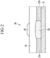
- FIG. 1 and FIG. 2 are schematic cross-sectional diagrams illustrating transistors according to example embodiments.
- a transistor according to at least one example embodiment may be a thin film transistor.
- the thin film transistor may include a thin film with a thickness of several nm to several ⁇ m.
- a transistor 10 may include a substrate 12, a gate electrode 14 on the substrate 12, and an insulation layer 16 covering the gate electrode 14.
- a source electrode 17a and a drain electrode 17b defining a channel region may be on the insulation layer 16.
- An active layer 18 may be in the channel region.
- the active layer 18 may include, for example, an organic semiconductor compound according to example embodiments.
- a source electrode 27a and a drain electrode 27b defining a channel region may be on a substrate 22, and an active layer 28 may be on the channel region.
- the active layer 28 may include an organic semiconductor compound according to example embodiments.
- An insulation layer 26 may cover the source electrode 27a, the drain electrode 27b, and the active layer 28.
- a gate electrode 24 may be on the insulation layer 26.
- the substrates 12 and 22 may include an inorganic material, an organic material, and/or a composite of an inorganic material and an organic material.
- the substrate organic material may include, for example, a plastic (e.g., polyethylenenaphthalate (PEN), polyethyleneterephthalate (PET), polycarbonate, polyvinylalcohol, polyacrylate, polyimide, polynorbornene, and polyethersulfone (PES)) and the inorganic material may include, for example, glass and/or metal.
- a plastic e.g., polyethylenenaphthalate (PEN), polyethyleneterephthalate (PET), polycarbonate, polyvinylalcohol, polyacrylate, polyimide, polynorbornene, and polyethersulfone (PES)
- the inorganic material may include, for example, glass and/or metal.
- the gate electrodes 14 and 24, source electrodes 17a and 27a, and drain electrodes 17b and 27b may include a generally-used metal and/or metal oxide, for example, gold (Au), silver (Ag), aluminum (Al), nickel (Ni), and/or indium tin oxide (ITO), but is not limited thereto.
- a generally-used metal and/or metal oxide for example, gold (Au), silver (Ag), aluminum (Al), nickel (Ni), and/or indium tin oxide (ITO), but is not limited thereto.
- the insulation layers 16 and 26 may include a generally-used insulator of high dielectric constant, for example, a ferroelectric insulator (e.g., Ba 0.33 Sr 0.66 TiO 3 (BST, barium strontium titanate), Al 2 O 3 , Ta 2 O 5 , La 2 O 5 , Y 2 O 3 , TiO 2 ), an inorganic insulator (e.g., PbZr 0.33 Ti 0.66 O 3 (PZT), Bi 4 Ti 3 O 12 , BaMgF 4 , SrBi 2 (TaNb) 2 O 9 , Ba(ZrTi)O 3 (BZT), BaTiO 3 , SrTiO 3 , SiO 2 , SiN x , AION and so on), or an organic insulator (e.g., polyimide, benzocyclobutene (BCB), parylene, polyacrylate, polyvinylalcohol, polyvinylphenol, and so on), but is not limited
- the organic semiconductor compound may be applicable to a memory device, an organic light emitting diode (OLED), a photosensor, a laser device, and so on.
- OLED organic light emitting diode
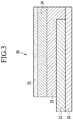
- FIG. 3 is a schematic cross-sectional diagram illustrating organic solar cells according to still other example embodiments.
- the organic solar cell 30 may include an anode 32 on a substrate 31.
- the substrate 31 may include any transparent material allowing an external light to enter without any particular limit.
- the transparent substrate may be glass and/or a plastic.
- plastics may include polyethyleneterephthalate (PET), polyethylene naphthalate (PEN), polycarbonate (PC), polypropylene (PP), polyimide (PI), triacetyl cellulose (TAC), a copolymer thereof, and/or the like.
- the anode 32 may be made of a high work function material for hole injection, for example, a transparent oxide (e.g., indium tin oxide (ITO), fluorine doped tin oxide (FTO), indium oxide, and/or the like).
- a hole transport layer (HTL) 33 may be on the anode 32.
- the hole transport layer (HTL) 33 may include a conductive polymer, for example, poly(3,4-ethylenedioxy-thiophene) (PEDOT) doped with poly(styrenesulfonate) (PSS) (PEDOT:PSS), polyaniline doped with poly(styrenesulfonic acid) (PAni:PSS), polypyrrole, poly(p-phenylenevinylene), poly[2-methoxy-5-(2'-ethyl-hexyloxy)-1,4-phenylene vinylene] (MEH-PPV), poly[2-methoxy-5-(3,7-dimethyloctyloxy)-1,4-phenylene-vinylene) (MDMO-PPV), poly(3-alkylthiophene), polythiophene, and the like, pentacene, CuPc, and/or a triphenyldiamine derivative (TPD).
- PEDOT poly(3,4-ethylenedioxy-thi
- a photoactive layer 34 may be on the hole transport layer (HTL) 33.
- the photoactive layer may include an electron donor (p-type semiconductor) material and an electron acceptor (n-type semiconductor) material.
- the electron donor may be one of the above-described organic semiconductor compounds.
- the electron acceptor may include fullerene with large electron affinity (C60, C70, C74, C76, C78, C82, C84, C720, C860), a fullerene derivative (e.g., 1-(3-methoxy-carbonyl)propyl-1-phenyl(6,6)C61 (PCBM)), or a mixture thereof.
- the organic semiconductor compound and the electron acceptor may be mixed in the photoactive layer 34 and/or form a bilayered photoactive layer 34 including two separate thin films.
- the organic semiconductor compound and a carbon-based material may be mixed in a weight ratio of about 1:0.5 to about 1:4. When the organic semiconductor compound and the carbon-based material are mixed within the range, efficiency of an organic solar cell may be improved.
- the photoactive layer 34 may be formed using a common method of coating an organic semiconductor compound mixture and an electron acceptor, for example, spraying, spin coating, dipping, printing, doctor-blading, sputtering, and/or the like.
- a thickness of the photoactive layer 34 may be about 5nm to about 2000 nm.
- a cathode 35 may be on the photoactive layer 34.
- the cathode 35 may include an alkali metal (e.g., lithium (Li), sodium (Na), and/or the like), an alkali-earth metal (e.g., beryllium (Be), magnesium (Mg), and/or the like), aluminum (Al), transition elements (e.g., silver (Ag), gold (Au), cobalt (Co), iridium (Ir), nickel (Ni), osmium (Os), palladium (Pd), platinum (Pt), and/or the like) a rare earth element, a semi-metal (e.g., selenium (Se), and/or the like), a metal alloy (e.g., a sodium-potassium alloy, a magnesium-indium alloy, an aluminum-lithium alloy, and/or the like), LiF/Al, and/or the like.
- an electron transport layer ETL
- ETL electron transport layer
- a photocurrent may be generated when a light is absorbed in the photoactive layer 34 and excites an electron-hole pair, the excited electron-hole pair may be diffused and reach a interface of an electron-acceptor and an electron-donor and may be separated into electrons and holes due to an electron affinity difference of the two materials at the interface.
- the electrons may move through the electron acceptor to a cathode 35 while the hole may move through the electron-donor to an anode 32.
- 3-hexylthiophene is reacted with N-bromosuccinimide (hereinafter, NBS) in the same amount in chloroform at room temperature for about 15 hours, preparing 2-bromo-3-hexylthiophene.
- NBS N-bromosuccinimide
- 2-bromo-3-hexylthiophene About 50 mmol of the 2-bromo-3-hexylthiophene is added with about 57 mmol of lithium diisopropylamine (hereinafter, LDA, about 2.0 M in a mixture of THF/hexane) to about 40 mL of an anhydrous THF during agitation at a temperature of about -80°C to about -90°C.
- LDA lithium diisopropylamine
- the resulting mixture is reacted at the same temperature for about 20 to about 30 minutes, and a THF solution of Me 3 SnCl (about 50 mmol) is added thereto.
- the mixture is agitated at about -50°C for about 1 hour.
- the agitated product is extracted with ether and water.
- the acquired organic layer is concentrated and distilled, obtaining 78 % of a yield of a colorless oily product.
- 2,5-bis(trimethylstannyl)thiophene (m is 1 in the following reaction scheme 3) and 2,5-bis(trimethylstannyl)bithiophene (m is 2 in the following reaction scheme 3) is synthesized referring to a synthesis method illustrated in J. Org. Chem., 1984, 49, 5250 .
- a palladium (0) compound, Pd(PPh 3 ) 4 as a polymerization catalyst is added thereto in an amount of about 0.1g, that is, 7.0 mol% based on the total monomers.
- the resulting mixture is reacted at about 90 °C for about 12 hours.
- the reaction solution is cooled down to room temperature and then, filtered, obtaining a polymer solid.
- the polymer solid is rinsed with a hydrochloric acid aqueous solution/chloroform twice, an ammonia aqueous solution/chloroform twice, and water/chloroform twice in order and then, recovered by using methanol, acetone, methylenechloride, and chloroform in a Soxhlet extraction method.
- FIG. 4 is an 1 H NMR spectrum of the organic semiconductor polymer represented by the above Chemical Formula 6-1 (3).
- 1 H NMR 300MHz, CDCl 3 ) ⁇ (ppm) : 0.86-1.83 (alkyl-CH2), 2.60 (Th-CH2, Head-to-Head), 2.80 (Th-CH2, Head-to-Tail), 3.92 (b, -O-CH2-), 6.76 - 7.60(Th-H, Ph-H), 7.78 (b, Th-H), 8.52 (b, Th-H), 9.13 (s, pyrido[3,4-b]pyrazine-H).
- FIG. 5 illustrates 1 H NMR spectrum of the organic semiconductor polymer represented by the above Chemical Formula 6-1 (2).
- 1 H NMR 300MHz, CDCl 3 ) ⁇ (ppm): 0.84-1.73 (alkyl-CH2), 2.60 (Th-CH2, Head-to-Head), 2.80 (Th-CH2, Head-to-Tail), 3.90 (b, -O-CH2-), 4.24 (b, -O-CH2-), 6.90 - 7.64(Th-H, Ph-H), 7.84 (b, Th-H), 8.55 (b, Th-H), 9.13 (s, pyrido[3,4-b]pyrazine-H).
- the reaction solution is cooled down to room temperature and is filtered, obtaining a polymer solid.
- the polymer solid is rinsed with a hydrochloric acid aqueous solution/chloroform twice, an ammonia aqueous solution/chloroform twice, and water/chloroform twice in order and is recovered in a Soxhlet extraction method by using methanol, acetone, methylene chloride, and chloroform.
- the hexylthiophene may have a ratio between head-to-tail (HT) : head-to-head (HH) of 0.89:0.11 with a significant regularity.
- 1 H NMR 300 MHz, CDCl3 ⁇ (ppm) : 0.92 -CH3, 1.10-1.72 (alkyl-CH2), 2.60 (Th-CH2, Head-to-Head), 2.81 (Th-CH2, Head-to-Tail), 3.94 (b, -O-CH2-, -N-CH2-), 6.95-7.43 (Th-H, Ph-H), 7.80 (b, Th-H), 8.53 (b, Th-H), 9.13 (s, pyrido[3,4-b]pyrazine-H).
- the organic semiconductor polymers according to Reference Examples 1-3 and Example 4 are respectively dissolved to have a concentration of about 1.0 wt% in chlorobenzene.
- the solution is coated in a spin-coating method.
- the coated product is baked at about 100°C for about one hour under a nitrogen atmosphere to form a film.
- FIG. 6 illustrates UV-Vis absorption spectrum of the organic semiconductor compound according to Reference Example 1. As shown in FIG. 6 , the organic semiconductor compound has a broad absorption spectrum ranging from about 400 nm to about 800 nm.
- a glass substrate is cleaned, chromium used as a gate electrode is deposited thereon at a thickness of about 100 nm (1000 ⁇ ) using, for example, a sputtering method, and SiO 2 used as a gate insulating layer is deposited on the gate electrode at a thickness of about 100 nm (1000 ⁇ ) using, for example, a CVD method.
- Au used as a source-drain electrode is deposited at a thickness of about 120 nm (1200 ⁇ ) on the gate insulating layer using, for example, a sputtering method.
- the substrate is rinsed with isopropyl alcohol for about 10 minutes and is dried before depositing organic semiconductor polymers.
- the organic semiconductor polymers are dipped in an octadecyl trichlorosilane solution diluted to have about 10mM of a concentration in chloroform for about 30 seconds, are rinsed with acetone, and dried, and each organic semiconductor polymer according to Reference Examples 1-3 and Example 4 is respectively dissolved to be about 1.0 wt% of a concentration in chlorobenzene.
- the solution is coated in a spin-coating method and is baked at about 150°C for about one hour under a nitrogen atmosphere, fabricating an OTFT device.
- the organic semiconductor polymers according to Reference Examples 1-3 and Example 4 are respectively mixed with a PCBM fullerene derivative ([6,6]-phenyl-C 61 -butyric acid methyl ester, a fullerene derivative) in a weight ratio of about 1:1 in a clorobenzene solvent, preparing a solution with about 10 mg/mL of a concentration.
- An ITO e.g., a conventional ITO
- PEDOT:PSS is spin-coated to be about 40nm thick.
- the coated ITO is baked at about 120°C for about 60 minutes.
- the solution is spin-coated to be about 100nm thick to form a photoactive layer on the PEDOT:PSS layer.
- LiF (about 0.6 nm)/AI (about 150 nm) is thermally deposited to form a cathode on the photoactive layer under about 1 X10 -4 Pa(1 X10 -6 mbar) of vacuum, fabricating an organic solar cell.
- Each organic solar cell is measured regarding current density-voltage (J sc -V oc ).
- the organic solar cells are operated using a conventional solar simulator, while being radiated by an AM 1.5G solar light with an intensity of 100 mW/cm 2 .
- the organic solar cell is measured regarding current density-voltage using a conventional source measurement unit.
- the intensity of the solar light is calibrated using a silicon solar cell as a reference.
- the organic solar cell including a mixture of the organic semiconductor polymer represented by Chemical Formula 6-1 (2) according to Reference Example 2 and PCBM in a weight ratio of 1 : 1 is measured regarding current density-voltage (J sc -V oc ). The result is provided in FIG. 7 . Based on the current density-voltage curved line of FIG. 7 , the power conversion efficiency (PCE) of the organic solar cell is calculated using the following Equation 1.
- PCE FF ⁇ V ⁇ I SC P in
- V oc may indicate open voltage of a solar cell
- I sc may indicate a short-circuit current
- FF may indicate a fill factor
- P in may indicate intensity of incident light in the solar cell.
- the organic solar cell including a mixture of the organic semiconductor polymer represented by Chemical Formula 6-1 (2) according to Reference Example 2 and PCBM in a weight ratio of 1:1 shows efficiency of 2.85%.
Landscapes
- Chemical & Material Sciences (AREA)
- Engineering & Computer Science (AREA)
- Organic Chemistry (AREA)
- Physics & Mathematics (AREA)
- Materials Engineering (AREA)
- Chemical Kinetics & Catalysis (AREA)
- Health & Medical Sciences (AREA)
- Medicinal Chemistry (AREA)
- Polymers & Plastics (AREA)
- Nanotechnology (AREA)
- Mathematical Physics (AREA)
- Crystallography & Structural Chemistry (AREA)
- Theoretical Computer Science (AREA)
- Spectroscopy & Molecular Physics (AREA)
- Electromagnetism (AREA)
- Thin Film Transistor (AREA)
- Electroluminescent Light Sources (AREA)
- Polyoxymethylene Polymers And Polymers With Carbon-To-Carbon Bonds (AREA)
- Photovoltaic Devices (AREA)
Claims (14)
- Organische Halbleiterverbindung, umfassend:
mindestens eine strukturelle Einheit gemäß der chemischen Formel 1: R1 ist Wasserstoff,und R2 ist ausgewählt aus einem der folgenden: einem Halogen, einer substituierten oder unsubstituierten C1 bis C20 linearen oder verzweigten Alkylgruppe, einer substituierten oder unsubstituierten C3- bis C20-Cycloalkylgruppe, einer substituierten oder unsubstituierten linearen oder verzweigten C1- bis C20-Alkoxygruppe, einer substituierten oder unsubstituierten C3- bis C20-Cycloalkyloxygruppe, einer substituierten oder unsubstituierten C6- bis C30-Arylgruppe, einer substituierten oder unsubstituierten C6- bis C30-Aryloxygruppe, einer substituierten oder unsubstituierten C2- bis C30-Heteroarylgruppe und einer Kombination dieser, undausgewählt aus einer C1- bis C20-Alkylgruppe, einer C1- bis C20-Alkoxygruppe und einer C3- bis C20-Cycloalkylgruppe,jedes X ist unabhängig ausgewählt aus -CR3=N-, -N=N- und -NR6-,Y ist ausgewählt aus -CR7=CR8-, -O-, -S-, -Se- und -NR9-, wobeiR3 und R6-R9 sind jeweils unabhängig ausgewählt aus einem der folgenden: Wasserstoff, einem Halogen, einer substituierten oder unsubstituierten C1 bis C20 linearen oder verzweigten Alkylgruppe, einer substituierten oder unsubstituierten C3-bis C20-Cycloalkylgruppe, einer substituierten oder unsubstituierten linearen oder verzweigten C1- bis C20-Alkoxygruppe, einer substituierten oder unsubstituierten C3-bis C20-Cycloalkyloxygruppe, einer substituierten oder unsubstituierten C6- bis C30-Arylgruppe, einer substituierten oder unsubstituierten C6- bis C30-Aryloxygruppe, einer substituierten oder unsubstituierten C2- bis C30-Heteroarylgruppe und einer Kombination dieser, undausgewählt aus einer C1- bis C20-Alkylgruppe, einer C1- bis C20-Alkoxygruppe und einer C3- bis C20-Cycloalkylgruppe,wobei eines einer CH2-Gruppe und einer Mehrzahl nicht benachbarter CH2-Gruppen optional substituiert ist mit -O-, -S-, -S(O)2-, -CO-, -OCO-, -C(O)O-, -CR51=CR52, -C≡C- oder -SiR53R54,wobei R51 bis R54 jeweils unabhängig ausgewählt sind aus Wasserstoff, einer substituierten oder unsubstituierten C1 bis C15 linearen oder verzweigten Alkylgruppe, einer substituierten oder unsubstituierten C3- bis C15-Cycloalkylgruppe, einer substituierten oder unsubstituierten C1- bis C15-Alkoxygruppe, einer substituierten oder unsubstituierten C6- bis C15-Arylgruppe, einer substituierten oder unsubstituierten C2-bis C15-Heteroarylgruppe und einer Kombination dieser, undwobei, wenn Y -CR7=CR8- ist, benachbarte R7 und R8 in einem kondensierten Ring verknüpft sein können,Z ist ausgewählt aus einer substituierten oder unsubstituierten C6- bis C40-Arylengruppe, einer substituierten oder unsubstituierten C4 bis C14 heteroaromatischen Ringgruppe und einer substituierten oder unsubstituierten C6 bis C30 kondensierten polycyclischen Gruppe, die eine heteroaromatische Ringgruppe aufweist, undp und q bezeichnen ein Molverhältnis jeder strukturellen Einheit und p/(p+q) liegt zwischen 0,5 und 0,95.
 - Organische Halbleiterverbindung nach Anspruch 1, wobei und p/(p+q) zwischen 0,6 und 0,9 liegt.
- Organische Halbleiterverbindung nach Anspruch 1 oder 2, wobei in der chemischen Formel 1 eine strukturelle Einheit gemäß der chemischen Formel 1A ausgewählt ist aus den strukturellen Einheiten gemäß der chemischen Formel 3,


- Organische Halbleiterverbindung nach einem der Ansprüche 1 bis 3, wobei in der chemischen Formel 1 eine strukturelle Einheit -Z- mindestens eine der strukturellen Einheiten gemäß der chemischen Formel 4 ist,

 wobei in der chemischen Formel 4 Q1 und Q2 jeweils eines der folgenden sind: S, CR64R65, NR66 oder SiR67R68,wobei R60 bis R68 jeweils unabhängig ausgewählt sind aus Wasserstoff, einer substituierten oder unsubstituierten C1 bis C15 linearen oder verzweigten Alkylgruppe, einer substituierten oder unsubstituierten C3- bis C15-Cycloalkylgruppe, einer substituierten oder unsubstituierten C1- bis C15-Alkoxygruppe, einer substituierten oder unsubstituierten C6- bis C15-Arylgruppe, einer substituierten oder unsubstituierten C2-bis C15-Heteroarylgruppe und einer Kombination davon, und wobei Wasserstoff in jedem Ring der chemischen Formel 4 optional substituiert ist mit einem Substituenten, der ausgewählt ist aus einem der folgenden: einer substituierten oder unsubstituierten C1 bis C15 linearen oder verzweigten Alkylgruppe, einer substituierten oder unsubstituierten C3- bis C15-Cycloalkylgruppe, einer substituierten oder unsubstituierten C1- bis C15-Alkoxygruppe, einer substituierten oder unsubstituierten C6- bis C15-Arylgruppe, einer substituierten oder unsubstituierten C2- bis C15-Heteroarylgruppe und einer Kombination davon.
 - Organische Halbleiterverbindung nach Anspruch 4, bei Abhängigkeit von Anspruch 4 von Anspruch 3, umfassend eine strukturelle Einheit gemäß der chemischen Formel 5,
 wobei in der chemischen Formel 5 R1 und R2 wie in der chemischen Formel 1 sind, wobei X und Y wie in der chemischen Formel 3 sind, wobei Z wie in der chemischen Formel 4 ist,wobei Z' mindestens eine funktionelle Gruppe gemäß der chemischen Formel 4 ist, wobei sich Z' von Z unterscheidet, undwobei p, q und r ein Molverhältnis jeder strukturellen Einheit bezeichnen, und wobei r/(p+q+r) zwischen 0,05 und 0,2 liegt.
 - Organische Halbleiterverbindung nach Anspruch 4, bei Abhängigkeit von Anspruch 4 von Anspruch 3, wobei die strukturelle Einheit der chemischen Formel 1A die strukturelle Einheit 3-4 ist, und wobei die strukturelle Einheit -Z- eine der strukturellen Einheiten 4-1, 4-3, 4-5, 4-6, 4-8, 4-10, 4-11 und 4-12 ist.
- Organische Hableiterverbindung nach Anspruch 1, umfassend mindestens eine der strukturellen Einheiten gemäß der chemischen Formel 6,

 wobei in der chemischen Formel 6 Ra ausgewählt ist aus einem der folgenden: einer substituierten oder unsubstituierten C1 bis C20 linearen oder verzweigten Alkylgruppe und einer substituierten oder unsubstituierten C1 bis C20 linearen oder verzweigten Alkoxygruppe, und wobei Rb-Rg jeweils unabhängig ausgewählt sind aus Wasserstoff, einer substituierten oder unsubstituierten C1 bis C20 linearen oder verzweigten Alkylgruppe und einer substituierten oder unsubstituierten C1 bis C20 linearen oder verzweigten Alkoxygruppe,wobei p und q für jede der strukturellen Einheiten (7), (8), (9), (10), (11), (12), (13) und (14) wie in der chemischen Formel 1 sind,wobei p, q und r ein Molverhältnis der strukturellen Einheit (15) bezeichnen,wobei p/(p+q) für jede der strukturellen Einheiten (7), (8), (9), (10), (11), (12), (13) und (14) zwischen 0,5 und 0,95 liegt,und wobei r/(p+q+r) für die strukturelle Einheit (15) zwischen 0,05 und 0,2 liegt.
 - Organische Halbleiterverbindung nach einem der Ansprüche 1 bis 7, wobei ein Zahlenmittel des Molekulargewichts (Mn) der organischen Halbleiterverbindung zwischen 5.000 und 200.000 liegt.
- Organische Halbleiterverbindung nach Anspruch 8, wobei ein Gewichtsmittel des Molekulargewichts (Mw) des organischen Halbleiters zwischen 10.000 und 500.000 liegt.
- Organische Halbleiterverbindung nach einem der Ansprüche 1 bis 9, wobei die organische Halbleiterverbindung vom p-Typ ist.
- Elektronische Vorrichtung, welche die organische Halbleiterverbindung nach einem der Ansprüche 1 bis 10 umfasst.
- Elektronische Vorrichtung nach Anspruch 11, wobei die elektronische Vorrichtung ein Transistor (10; 20) ist.
- Elektronische Vorrichtung nach Anspruch 12, wobei der Transistor (10; 20) folgendes aufweist:eine Gate-Elektrode (14; 24), die auf einem Substrat (12; 22) positioniert ist;eine Source-Elektrode (17a; 27a) und eine Drain-Elektrode (17b; 27b), die zueinander zeigen und eine Kanalregion definieren;eine Isolationsschicht (16; 26), welche die Source-Elektrode (17a; 27a) und die Drain-Elektrode (17b; 27b) von der Gate-Elektrode (14; 24) trennt; undeine aktive Schicht (18; 28), welche die organische Halbleiterverbindung in der Kanalregion zwischen der Source-Elektrode (17a; 27a) und der Drain-Elektrode (17b; 27b) aufweist.
- Elektronische Vorrichtung nach Anspruch 11, wobei die elektronische Vorrichtung eine organische Solarzelle (30) ist.
Applications Claiming Priority (1)
| Application Number | Priority Date | Filing Date | Title |
|---|---|---|---|
| KR1020110000692A KR102011872B1 (ko) | 2011-01-04 | 2011-01-04 | 낮은 밴드 갭을 갖는 유기 반도체 화합물 및 이를 포함하는 트랜지스터와 전자 소자 |
Publications (2)
| Publication Number | Publication Date |
|---|---|
| EP2472625A1 EP2472625A1 (de) | 2012-07-04 |
| EP2472625B1 true EP2472625B1 (de) | 2020-04-01 |
Family
ID=45401015
Family Applications (1)
| Application Number | Title | Priority Date | Filing Date |
|---|---|---|---|
| EP12150078.9A Not-in-force EP2472625B1 (de) | 2011-01-04 | 2012-01-03 | Organische Halbleiterverbindungen mit geringen Bandabständen sowie elektronische Vorrichtungen damit |
Country Status (5)
| Country | Link |
|---|---|
| US (1) | US9379329B2 (de) |
| EP (1) | EP2472625B1 (de) |
| JP (1) | JP5946273B2 (de) |
| KR (1) | KR102011872B1 (de) |
| CN (1) | CN102585173B (de) |
Families Citing this family (4)
| Publication number | Priority date | Publication date | Assignee | Title |
|---|---|---|---|---|
| WO2014094955A1 (en) | 2012-12-18 | 2014-06-26 | Merck Patent Gmbh | Polymer comprising a thiadiazol group, the production of such polymer and its use in organic electronic devices |
| TW201501340A (zh) * | 2013-06-27 | 2015-01-01 | Inst Nuclear Energy Res Atomic Energy Council | 製備大面積有機太陽能電池之方法 |
| US9876184B2 (en) * | 2013-08-28 | 2018-01-23 | Taiwan Semiconductor Manufacturing Company, Ltd. | Organic photosensitive device with an electron-blocking and hole-transport layer |
| KR102168174B1 (ko) | 2014-03-19 | 2020-10-20 | 삼성전자주식회사 | 니켈 화합물 및 이를 이용한 박막 형성 방법 |
Family Cites Families (19)
| Publication number | Priority date | Publication date | Assignee | Title |
|---|---|---|---|---|
| US5946551A (en) | 1997-03-25 | 1999-08-31 | Dimitrakopoulos; Christos Dimitrios | Fabrication of thin film effect transistor comprising an organic semiconductor and chemical solution deposited metal oxide gate dielectric |
| US6215130B1 (en) | 1998-08-20 | 2001-04-10 | Lucent Technologies Inc. | Thin film transistors |
| JP4404550B2 (ja) | 2001-01-24 | 2010-01-27 | ケンブリッジ ディスプレイ テクノロジー リミテッド | 光学デバイスに使用すべきポリマーの調製に使用するモノマー |
| KR101007787B1 (ko) | 2003-12-08 | 2011-01-14 | 삼성전자주식회사 | 퀴녹살린환을 주쇄에 포함하는 유기박막 트랜지스터용유기반도체 고분자 |
| CN100583485C (zh) | 2004-09-24 | 2010-01-20 | 普莱克斯托尼克斯公司 | 含杂原子立体规则性聚(3-取代噻吩)的光电池 |
| KR101224708B1 (ko) | 2004-10-19 | 2013-01-21 | 삼성전자주식회사 | (올리고티오펜-아릴렌) 유도체 및 이를 이용한유기박막트랜지스터 |
| EP1864300A4 (de) | 2005-03-16 | 2009-12-02 | Plextronics Inc | Copolymere aus lösbaren poly(thiophenen) mit verbesserter elektronischer leistungsfähigkeit |
| KR101314931B1 (ko) | 2006-10-30 | 2013-10-04 | 삼성전자주식회사 | 유기 고분자 반도체, 이의 제조방법 및 이를 이용한 양극성 유기 박막 트랜지스터 |
| JP2008208289A (ja) | 2007-02-28 | 2008-09-11 | Sumitomo Chemical Co Ltd | 芳香族重合体およびそれを用いた有機光電変換素子 |
| US20080262183A1 (en) | 2007-04-17 | 2008-10-23 | Lutz Uwe Lehmann | Dithienopyrrole-containing copolymers |
| WO2009125647A1 (ja) | 2008-04-11 | 2009-10-15 | 東レ株式会社 | 電子供与性有機材料、光起電力素子用材料および光起電力素子 |
| EP2287936B1 (de) * | 2008-05-12 | 2016-05-04 | Toray Industries, Inc. | Kohlenstoffnanoröhrchenverbund, organischer halbleiterverbund und feldeffekttransistor |
| US8367798B2 (en) | 2008-09-29 | 2013-02-05 | The Regents Of The University Of California | Active materials for photoelectric devices and devices that use the materials |
| JP5655267B2 (ja) | 2008-11-10 | 2015-01-21 | 東レ株式会社 | キノキサリン化合物、これを用いた電子供与性有機材料、光起電力素子用材料および光起電力素子 |
| JP5533646B2 (ja) | 2009-01-20 | 2014-06-25 | 東レ株式会社 | 光起電力素子用材料および光起電力素子 |
| WO2010135701A1 (en) | 2009-05-21 | 2010-11-25 | Polyera Corporation | Conjugated polymers and their use in optoelectronic devices |
| WO2010138566A2 (en) | 2009-05-26 | 2010-12-02 | University Of Florida Research Foundation, Inc. | Green soluble conjugated polymers with high charge carrier mobilities |
| KR101648072B1 (ko) * | 2009-07-03 | 2016-08-12 | 삼성전자 주식회사 | 유기 반도체 고분자 및 이를 포함하는 트랜지스터 |
| WO2011138885A1 (ja) | 2010-05-06 | 2011-11-10 | 住友化学株式会社 | 高分子化合物及びそれを用いた有機光電変換素子 |
-
2011
- 2011-01-04 KR KR1020110000692A patent/KR102011872B1/ko not_active Expired - Fee Related
- 2011-08-17 US US13/211,810 patent/US9379329B2/en active Active
- 2011-12-29 JP JP2011290399A patent/JP5946273B2/ja not_active Expired - Fee Related
-
2012
- 2012-01-03 EP EP12150078.9A patent/EP2472625B1/de not_active Not-in-force
- 2012-01-04 CN CN201210001157.7A patent/CN102585173B/zh not_active Expired - Fee Related
Non-Patent Citations (1)
| Title |
|---|
| None * |
Also Published As
| Publication number | Publication date |
|---|---|
| US20120168727A1 (en) | 2012-07-05 |
| EP2472625A1 (de) | 2012-07-04 |
| KR102011872B1 (ko) | 2019-08-19 |
| CN102585173B (zh) | 2016-11-02 |
| CN102585173A (zh) | 2012-07-18 |
| KR20120079423A (ko) | 2012-07-12 |
| JP2012140624A (ja) | 2012-07-26 |
| JP5946273B2 (ja) | 2016-07-06 |
| US9379329B2 (en) | 2016-06-28 |
Similar Documents
| Publication | Publication Date | Title |
|---|---|---|
| US8367798B2 (en) | Active materials for photoelectric devices and devices that use the materials | |
| CN102449030B (zh) | 用于有机半导体器件中的二酮基吡咯并吡咯聚合物 | |
| US8871884B2 (en) | Copolymer semiconductors comprising thiazolothiazole or benzobisthiazole, or benzobisoxazole electron acceptor subunits, and electron donor subunits, and their uses in transistors and solar cells | |
| JP5583133B2 (ja) | 有機電界効果トランジスタに使用するためのジケトピロロピロールポリマー | |
| KR101546985B1 (ko) | 피롤로피롤 유도체, 그의 제조 및 용도 | |
| JP5635070B2 (ja) | 有機半導体デバイスでの使用のためのジケトピロロピロールポリマー | |
| KR101764436B1 (ko) | 유기 반도체 장치에 사용하기 위한 디케토피롤로피롤 중합체 | |
| JP2014512100A (ja) | 電気光学デバイスの活性物質および電気光学デバイス | |
| CN101479272A (zh) | 作为有机半导体的二酮基吡咯并吡咯聚合物 | |
| EP2270064B1 (de) | Organisches Halbleiterpolymer, Transistor mit einem organischen Halbleiterpolymer und Herstellungsverfahren dafür | |
| WO2008143838A1 (en) | Aryl-substituted conjugated polymers | |
| US9379329B2 (en) | Low band-gap organic semiconductor compounds, and transistors and electronic devices including the same | |
| US20150194608A1 (en) | Building block for low bandgap conjugated polymers | |
| Patil et al. | Synthesis and photovoltaic properties of narrow band gap copolymers of dithieno [3, 2-b: 2′, 3′-d] thiophene and diketopyrrolopyrrole | |
| US8933441B2 (en) | Organic electronic device | |
| KR101935466B1 (ko) | 유기 전자 소자 | |
| KR101947020B1 (ko) | 낮은 밴드 갭을 갖는 유기 반도체 화합물 및 이를 포함하는 트랜지스터와 전자 소자 | |
| KR101504864B1 (ko) | 공액성 곁사슬이 도입된 고분자 및 이를 이용한 광전자소자 | |
| Nicoletta | Design and synthesis of new processable materials for application in organic devices. | |
| CN110536915A (zh) | 用于电子和光子应用的垂直苯并二噻吩基给体-受体聚合物 |
Legal Events
| Date | Code | Title | Description |
|---|---|---|---|
| 17P | Request for examination filed |
Effective date: 20120330 |
|
| AK | Designated contracting states |
Kind code of ref document: A1 Designated state(s): AL AT BE BG CH CY CZ DE DK EE ES FI FR GB GR HR HU IE IS IT LI LT LU LV MC MK MT NL NO PL PT RO RS SE SI SK SM TR |
|
| AX | Request for extension of the european patent |
Extension state: BA ME |
|
| PUAI | Public reference made under article 153(3) epc to a published international application that has entered the european phase |
Free format text: ORIGINAL CODE: 0009012 |
|
| RAP1 | Party data changed (applicant data changed or rights of an application transferred) |
Owner name: SAMSUNG ELECTRONICS CO., LTD. |
|
| STAA | Information on the status of an ep patent application or granted ep patent |
Free format text: STATUS: EXAMINATION IS IN PROGRESS |
|
| 17Q | First examination report despatched |
Effective date: 20180518 |
|
| REG | Reference to a national code |
Ref country code: DE Ref legal event code: R079 Ref document number: 602012068850 Country of ref document: DE Free format text: PREVIOUS MAIN CLASS: H01L0051000000 Ipc: B82Y0010000000 |
|
| RIC1 | Information provided on ipc code assigned before grant |
Ipc: C08G 61/12 20060101ALI20190730BHEP Ipc: H01L 51/00 20060101ALI20190730BHEP Ipc: H01L 51/05 20060101ALN20190730BHEP Ipc: C09B 69/10 20060101ALI20190730BHEP Ipc: B82Y 10/00 20110101AFI20190730BHEP Ipc: H01L 51/42 20060101ALN20190730BHEP |
|
| GRAP | Despatch of communication of intention to grant a patent |
Free format text: ORIGINAL CODE: EPIDOSNIGR1 |
|
| STAA | Information on the status of an ep patent application or granted ep patent |
Free format text: STATUS: GRANT OF PATENT IS INTENDED |
|
| INTG | Intention to grant announced |
Effective date: 20191009 |
|
| GRAS | Grant fee paid |
Free format text: ORIGINAL CODE: EPIDOSNIGR3 |
|
| GRAA | (expected) grant |
Free format text: ORIGINAL CODE: 0009210 |
|
| STAA | Information on the status of an ep patent application or granted ep patent |
Free format text: STATUS: THE PATENT HAS BEEN GRANTED |
|
| AK | Designated contracting states |
Kind code of ref document: B1 Designated state(s): AL AT BE BG CH CY CZ DE DK EE ES FI FR GB GR HR HU IE IS IT LI LT LU LV MC MK MT NL NO PL PT RO RS SE SI SK SM TR |
|
| REG | Reference to a national code |
Ref country code: GB Ref legal event code: FG4D |
|
| REG | Reference to a national code |
Ref country code: AT Ref legal event code: REF Ref document number: 1251135 Country of ref document: AT Kind code of ref document: T Effective date: 20200415 Ref country code: CH Ref legal event code: EP |
|
| REG | Reference to a national code |
Ref country code: DE Ref legal event code: R096 Ref document number: 602012068850 Country of ref document: DE |
|
| REG | Reference to a national code |
Ref country code: IE Ref legal event code: FG4D |
|
| PG25 | Lapsed in a contracting state [announced via postgrant information from national office to epo] |
Ref country code: BG Free format text: LAPSE BECAUSE OF FAILURE TO SUBMIT A TRANSLATION OF THE DESCRIPTION OR TO PAY THE FEE WITHIN THE PRESCRIBED TIME-LIMIT Effective date: 20200701 |
|
| REG | Reference to a national code |
Ref country code: NL Ref legal event code: MP Effective date: 20200401 |
|
| REG | Reference to a national code |
Ref country code: LT Ref legal event code: MG4D |
|
| PG25 | Lapsed in a contracting state [announced via postgrant information from national office to epo] |
Ref country code: NL Free format text: LAPSE BECAUSE OF FAILURE TO SUBMIT A TRANSLATION OF THE DESCRIPTION OR TO PAY THE FEE WITHIN THE PRESCRIBED TIME-LIMIT Effective date: 20200401 Ref country code: IS Free format text: LAPSE BECAUSE OF FAILURE TO SUBMIT A TRANSLATION OF THE DESCRIPTION OR TO PAY THE FEE WITHIN THE PRESCRIBED TIME-LIMIT Effective date: 20200801 Ref country code: CZ Free format text: LAPSE BECAUSE OF FAILURE TO SUBMIT A TRANSLATION OF THE DESCRIPTION OR TO PAY THE FEE WITHIN THE PRESCRIBED TIME-LIMIT Effective date: 20200401 Ref country code: FI Free format text: LAPSE BECAUSE OF FAILURE TO SUBMIT A TRANSLATION OF THE DESCRIPTION OR TO PAY THE FEE WITHIN THE PRESCRIBED TIME-LIMIT Effective date: 20200401 Ref country code: NO Free format text: LAPSE BECAUSE OF FAILURE TO SUBMIT A TRANSLATION OF THE DESCRIPTION OR TO PAY THE FEE WITHIN THE PRESCRIBED TIME-LIMIT Effective date: 20200701 Ref country code: SE Free format text: LAPSE BECAUSE OF FAILURE TO SUBMIT A TRANSLATION OF THE DESCRIPTION OR TO PAY THE FEE WITHIN THE PRESCRIBED TIME-LIMIT Effective date: 20200401 Ref country code: GR Free format text: LAPSE BECAUSE OF FAILURE TO SUBMIT A TRANSLATION OF THE DESCRIPTION OR TO PAY THE FEE WITHIN THE PRESCRIBED TIME-LIMIT Effective date: 20200702 Ref country code: PT Free format text: LAPSE BECAUSE OF FAILURE TO SUBMIT A TRANSLATION OF THE DESCRIPTION OR TO PAY THE FEE WITHIN THE PRESCRIBED TIME-LIMIT Effective date: 20200817 Ref country code: LT Free format text: LAPSE BECAUSE OF FAILURE TO SUBMIT A TRANSLATION OF THE DESCRIPTION OR TO PAY THE FEE WITHIN THE PRESCRIBED TIME-LIMIT Effective date: 20200401 |
|
| REG | Reference to a national code |
Ref country code: AT Ref legal event code: MK05 Ref document number: 1251135 Country of ref document: AT Kind code of ref document: T Effective date: 20200401 |
|
| PG25 | Lapsed in a contracting state [announced via postgrant information from national office to epo] |
Ref country code: RS Free format text: LAPSE BECAUSE OF FAILURE TO SUBMIT A TRANSLATION OF THE DESCRIPTION OR TO PAY THE FEE WITHIN THE PRESCRIBED TIME-LIMIT Effective date: 20200401 Ref country code: LV Free format text: LAPSE BECAUSE OF FAILURE TO SUBMIT A TRANSLATION OF THE DESCRIPTION OR TO PAY THE FEE WITHIN THE PRESCRIBED TIME-LIMIT Effective date: 20200401 Ref country code: HR Free format text: LAPSE BECAUSE OF FAILURE TO SUBMIT A TRANSLATION OF THE DESCRIPTION OR TO PAY THE FEE WITHIN THE PRESCRIBED TIME-LIMIT Effective date: 20200401 |
|
| PG25 | Lapsed in a contracting state [announced via postgrant information from national office to epo] |
Ref country code: AL Free format text: LAPSE BECAUSE OF FAILURE TO SUBMIT A TRANSLATION OF THE DESCRIPTION OR TO PAY THE FEE WITHIN THE PRESCRIBED TIME-LIMIT Effective date: 20200401 |
|
| REG | Reference to a national code |
Ref country code: DE Ref legal event code: R097 Ref document number: 602012068850 Country of ref document: DE |
|
| PG25 | Lapsed in a contracting state [announced via postgrant information from national office to epo] |
Ref country code: ES Free format text: LAPSE BECAUSE OF FAILURE TO SUBMIT A TRANSLATION OF THE DESCRIPTION OR TO PAY THE FEE WITHIN THE PRESCRIBED TIME-LIMIT Effective date: 20200401 Ref country code: EE Free format text: LAPSE BECAUSE OF FAILURE TO SUBMIT A TRANSLATION OF THE DESCRIPTION OR TO PAY THE FEE WITHIN THE PRESCRIBED TIME-LIMIT Effective date: 20200401 Ref country code: SM Free format text: LAPSE BECAUSE OF FAILURE TO SUBMIT A TRANSLATION OF THE DESCRIPTION OR TO PAY THE FEE WITHIN THE PRESCRIBED TIME-LIMIT Effective date: 20200401 Ref country code: IT Free format text: LAPSE BECAUSE OF FAILURE TO SUBMIT A TRANSLATION OF THE DESCRIPTION OR TO PAY THE FEE WITHIN THE PRESCRIBED TIME-LIMIT Effective date: 20200401 Ref country code: AT Free format text: LAPSE BECAUSE OF FAILURE TO SUBMIT A TRANSLATION OF THE DESCRIPTION OR TO PAY THE FEE WITHIN THE PRESCRIBED TIME-LIMIT Effective date: 20200401 Ref country code: DK Free format text: LAPSE BECAUSE OF FAILURE TO SUBMIT A TRANSLATION OF THE DESCRIPTION OR TO PAY THE FEE WITHIN THE PRESCRIBED TIME-LIMIT Effective date: 20200401 Ref country code: RO Free format text: LAPSE BECAUSE OF FAILURE TO SUBMIT A TRANSLATION OF THE DESCRIPTION OR TO PAY THE FEE WITHIN THE PRESCRIBED TIME-LIMIT Effective date: 20200401 |
|
| PLBE | No opposition filed within time limit |
Free format text: ORIGINAL CODE: 0009261 |
|
| STAA | Information on the status of an ep patent application or granted ep patent |
Free format text: STATUS: NO OPPOSITION FILED WITHIN TIME LIMIT |
|
| PG25 | Lapsed in a contracting state [announced via postgrant information from national office to epo] |
Ref country code: PL Free format text: LAPSE BECAUSE OF FAILURE TO SUBMIT A TRANSLATION OF THE DESCRIPTION OR TO PAY THE FEE WITHIN THE PRESCRIBED TIME-LIMIT Effective date: 20200401 Ref country code: SK Free format text: LAPSE BECAUSE OF FAILURE TO SUBMIT A TRANSLATION OF THE DESCRIPTION OR TO PAY THE FEE WITHIN THE PRESCRIBED TIME-LIMIT Effective date: 20200401 |
|
| 26N | No opposition filed |
Effective date: 20210112 |
|
| PG25 | Lapsed in a contracting state [announced via postgrant information from national office to epo] |
Ref country code: SI Free format text: LAPSE BECAUSE OF FAILURE TO SUBMIT A TRANSLATION OF THE DESCRIPTION OR TO PAY THE FEE WITHIN THE PRESCRIBED TIME-LIMIT Effective date: 20200401 |
|
| PG25 | Lapsed in a contracting state [announced via postgrant information from national office to epo] |
Ref country code: MC Free format text: LAPSE BECAUSE OF FAILURE TO SUBMIT A TRANSLATION OF THE DESCRIPTION OR TO PAY THE FEE WITHIN THE PRESCRIBED TIME-LIMIT Effective date: 20200401 |
|
| REG | Reference to a national code |
Ref country code: CH Ref legal event code: PL |
|
| PG25 | Lapsed in a contracting state [announced via postgrant information from national office to epo] |
Ref country code: LU Free format text: LAPSE BECAUSE OF NON-PAYMENT OF DUE FEES Effective date: 20210103 |
|
| REG | Reference to a national code |
Ref country code: BE Ref legal event code: MM Effective date: 20210131 |
|
| PG25 | Lapsed in a contracting state [announced via postgrant information from national office to epo] |
Ref country code: LI Free format text: LAPSE BECAUSE OF NON-PAYMENT OF DUE FEES Effective date: 20210131 Ref country code: CH Free format text: LAPSE BECAUSE OF NON-PAYMENT OF DUE FEES Effective date: 20210131 |
|
| PG25 | Lapsed in a contracting state [announced via postgrant information from national office to epo] |
Ref country code: IE Free format text: LAPSE BECAUSE OF NON-PAYMENT OF DUE FEES Effective date: 20210103 |
|
| PG25 | Lapsed in a contracting state [announced via postgrant information from national office to epo] |
Ref country code: BE Free format text: LAPSE BECAUSE OF NON-PAYMENT OF DUE FEES Effective date: 20210131 |
|
| PG25 | Lapsed in a contracting state [announced via postgrant information from national office to epo] |
Ref country code: HU Free format text: LAPSE BECAUSE OF FAILURE TO SUBMIT A TRANSLATION OF THE DESCRIPTION OR TO PAY THE FEE WITHIN THE PRESCRIBED TIME-LIMIT; INVALID AB INITIO Effective date: 20120103 Ref country code: CY Free format text: LAPSE BECAUSE OF FAILURE TO SUBMIT A TRANSLATION OF THE DESCRIPTION OR TO PAY THE FEE WITHIN THE PRESCRIBED TIME-LIMIT Effective date: 20200401 |
|
| P01 | Opt-out of the competence of the unified patent court (upc) registered |
Effective date: 20230519 |
|
| PGFP | Annual fee paid to national office [announced via postgrant information from national office to epo] |
Ref country code: GB Payment date: 20231220 Year of fee payment: 13 |
|
| PGFP | Annual fee paid to national office [announced via postgrant information from national office to epo] |
Ref country code: FR Payment date: 20231222 Year of fee payment: 13 |
|
| PG25 | Lapsed in a contracting state [announced via postgrant information from national office to epo] |
Ref country code: MK Free format text: LAPSE BECAUSE OF FAILURE TO SUBMIT A TRANSLATION OF THE DESCRIPTION OR TO PAY THE FEE WITHIN THE PRESCRIBED TIME-LIMIT Effective date: 20200401 |
|
| PGFP | Annual fee paid to national office [announced via postgrant information from national office to epo] |
Ref country code: DE Payment date: 20231220 Year of fee payment: 13 |
|
| PG25 | Lapsed in a contracting state [announced via postgrant information from national office to epo] |
Ref country code: TR Free format text: LAPSE BECAUSE OF FAILURE TO SUBMIT A TRANSLATION OF THE DESCRIPTION OR TO PAY THE FEE WITHIN THE PRESCRIBED TIME-LIMIT Effective date: 20200401 |
|
| PG25 | Lapsed in a contracting state [announced via postgrant information from national office to epo] |
Ref country code: MT Free format text: LAPSE BECAUSE OF FAILURE TO SUBMIT A TRANSLATION OF THE DESCRIPTION OR TO PAY THE FEE WITHIN THE PRESCRIBED TIME-LIMIT Effective date: 20200401 |
|
| REG | Reference to a national code |
Ref country code: DE Ref legal event code: R119 Ref document number: 602012068850 Country of ref document: DE |
|
| GBPC | Gb: european patent ceased through non-payment of renewal fee |
Effective date: 20250103 |
|
| PG25 | Lapsed in a contracting state [announced via postgrant information from national office to epo] |
Ref country code: DE Free format text: LAPSE BECAUSE OF NON-PAYMENT OF DUE FEES Effective date: 20250801 |
|
| PG25 | Lapsed in a contracting state [announced via postgrant information from national office to epo] |
Ref country code: GB Free format text: LAPSE BECAUSE OF NON-PAYMENT OF DUE FEES Effective date: 20250103 |
|
| PG25 | Lapsed in a contracting state [announced via postgrant information from national office to epo] |
Ref country code: FR Free format text: LAPSE BECAUSE OF NON-PAYMENT OF DUE FEES Effective date: 20250131 |