EP2270896A1 - Organische el-anzeigetafel - Google Patents
Organische el-anzeigetafel Download PDFInfo
- Publication number
- EP2270896A1 EP2270896A1 EP09700056A EP09700056A EP2270896A1 EP 2270896 A1 EP2270896 A1 EP 2270896A1 EP 09700056 A EP09700056 A EP 09700056A EP 09700056 A EP09700056 A EP 09700056A EP 2270896 A1 EP2270896 A1 EP 2270896A1
- Authority
- EP
- European Patent Office
- Prior art keywords
- organic
- light emitting
- hole injection
- display panel
- injection layer
- Prior art date
- Legal status (The legal status is an assumption and is not a legal conclusion. Google has not performed a legal analysis and makes no representation as to the accuracy of the status listed.)
- Granted
Links
Images



Classifications
-
- H—ELECTRICITY
- H10—SEMICONDUCTOR DEVICES; ELECTRIC SOLID-STATE DEVICES NOT OTHERWISE PROVIDED FOR
- H10K—ORGANIC ELECTRIC SOLID-STATE DEVICES
- H10K59/00—Integrated devices, or assemblies of multiple devices, comprising at least one organic light-emitting element covered by group H10K50/00
- H10K59/10—OLED displays
- H10K59/12—Active-matrix OLED [AMOLED] displays
- H10K59/124—Insulating layers formed between TFT elements and OLED elements
-
- H—ELECTRICITY
- H10—SEMICONDUCTOR DEVICES; ELECTRIC SOLID-STATE DEVICES NOT OTHERWISE PROVIDED FOR
- H10K—ORGANIC ELECTRIC SOLID-STATE DEVICES
- H10K50/00—Organic light-emitting devices
- H10K50/10—OLEDs or polymer light-emitting diodes [PLED]
- H10K50/17—Carrier injection layers
-
- H—ELECTRICITY
- H10—SEMICONDUCTOR DEVICES; ELECTRIC SOLID-STATE DEVICES NOT OTHERWISE PROVIDED FOR
- H10K—ORGANIC ELECTRIC SOLID-STATE DEVICES
- H10K50/00—Organic light-emitting devices
- H10K50/80—Constructional details
- H10K50/805—Electrodes
- H10K50/81—Anodes
- H10K50/813—Anodes characterised by their shape
-
- H—ELECTRICITY
- H10—SEMICONDUCTOR DEVICES; ELECTRIC SOLID-STATE DEVICES NOT OTHERWISE PROVIDED FOR
- H10K—ORGANIC ELECTRIC SOLID-STATE DEVICES
- H10K50/00—Organic light-emitting devices
- H10K50/80—Constructional details
- H10K50/85—Arrangements for extracting light from the devices
-
- H—ELECTRICITY
- H10—SEMICONDUCTOR DEVICES; ELECTRIC SOLID-STATE DEVICES NOT OTHERWISE PROVIDED FOR
- H10K—ORGANIC ELECTRIC SOLID-STATE DEVICES
- H10K59/00—Integrated devices, or assemblies of multiple devices, comprising at least one organic light-emitting element covered by group H10K50/00
- H10K59/10—OLED displays
- H10K59/12—Active-matrix OLED [AMOLED] displays
- H10K59/122—Pixel-defining structures or layers, e.g. banks
-
- H—ELECTRICITY
- H10—SEMICONDUCTOR DEVICES; ELECTRIC SOLID-STATE DEVICES NOT OTHERWISE PROVIDED FOR
- H10K—ORGANIC ELECTRIC SOLID-STATE DEVICES
- H10K59/00—Integrated devices, or assemblies of multiple devices, comprising at least one organic light-emitting element covered by group H10K50/00
- H10K59/10—OLED displays
- H10K59/17—Passive-matrix OLED displays
- H10K59/173—Passive-matrix OLED displays comprising banks or shadow masks
-
- H—ELECTRICITY
- H10—SEMICONDUCTOR DEVICES; ELECTRIC SOLID-STATE DEVICES NOT OTHERWISE PROVIDED FOR
- H10K—ORGANIC ELECTRIC SOLID-STATE DEVICES
- H10K59/00—Integrated devices, or assemblies of multiple devices, comprising at least one organic light-emitting element covered by group H10K50/00
- H10K59/80—Constructional details
- H10K59/805—Electrodes
- H10K59/8051—Anodes
- H10K59/80515—Anodes characterised by their shape
-
- H—ELECTRICITY
- H10—SEMICONDUCTOR DEVICES; ELECTRIC SOLID-STATE DEVICES NOT OTHERWISE PROVIDED FOR
- H10K—ORGANIC ELECTRIC SOLID-STATE DEVICES
- H10K59/00—Integrated devices, or assemblies of multiple devices, comprising at least one organic light-emitting element covered by group H10K50/00
- H10K59/80—Constructional details
- H10K59/875—Arrangements for extracting light from the devices
-
- H—ELECTRICITY
- H10—SEMICONDUCTOR DEVICES; ELECTRIC SOLID-STATE DEVICES NOT OTHERWISE PROVIDED FOR
- H10K—ORGANIC ELECTRIC SOLID-STATE DEVICES
- H10K71/00—Manufacture or treatment specially adapted for the organic devices covered by this subclass
- H10K71/10—Deposition of organic active material
- H10K71/12—Deposition of organic active material using liquid deposition, e.g. spin coating
-
- H—ELECTRICITY
- H10—SEMICONDUCTOR DEVICES; ELECTRIC SOLID-STATE DEVICES NOT OTHERWISE PROVIDED FOR
- H10K—ORGANIC ELECTRIC SOLID-STATE DEVICES
- H10K2102/00—Constructional details relating to the organic devices covered by this subclass
- H10K2102/301—Details of OLEDs
Definitions
- the present invention relates to an organic EL display panel and a manufacturing method thereof.
- An organic EL device which is a display device, is a light emitting element exploiting electro-luminescence of organic compounds.
- An organic EL device has a cathode, an anode, and an electroluminescent organic light emitting layer provided between the electrodes.
- Organic light emitting layer can be roughly classified into two categories: the organic light emitting layer containing combinations of small molecular organic compounds (host material and dopant material) and the organic light emitting layer containing polymer.
- Examples of electro-luminescent polymer include polyphenylenevinylene (also referred to as PPV) and its derivatives.
- PPV polyphenylenevinylene
- organic EL elements In an organic EL display panel using organic EL devices, organic EL elements (sub pixels) are arranged in matrix form on the substrate. In an organic EL display panel, organic EL element emits red (R), green (G), or blue (B) light.
- R red
- G green
- B blue
- An organic light emitting layer containing polymer is formed by applying a polymer ink containing, for example, organic light emitting materials and solvents, to an anode with ink jet or the like. Therefore, when an ink that contains an organic light emitting material is applied to each sub pixel of an organic EL display panel, it is necessary to prevent ink from intruding into adjacent sub pixels.
- Patent Document 1 discloses a method for preventing a polymer ink from intruding into adjacent sub pixels by providing banks defining each sub pixel and by dropping a polymer ink accurately on each sub pixel.
- Patent Documents 2 to 4 disclose techniques for improving the viewing angle of an organic EL display, by forming a plurality of concave and convex shapes on the surface of an anode of organic EL element to make an organic light emitting layer concavo-convex.
- Patent Documents 5 to 8 disclose techniques of enlarging a surface of an anode by forming fine concave and convex shapes on the surface of an anode of organic EL element to improve the light emission efficiency by increasing a current to supply to an organic light emitting layer.
- Patent Document 9 discloses a technique for improving the efficiency of light emission of a pixel by forming concave parts and convex parts in an organic light emitting layer and by suppressing light emission from the convex parts.
- Patent Documents 10 and 11 disclose techniques for efficiently utilizing light of the organic light emitting layer by making the organic light emitting layer concavely curved. Further, in Patent Documents 10 and 11, an organic light emitting layer is formed with the deposition method.
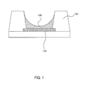
- the ink is attracted to banks 107 in the process of drying the ink.
- cases occur where the center part of formed organic light emitting layer 109 is dented and the surface of organic light emitting layer 109 curves concavely. If the surface of organic light emitting layer 109 curves concavely, the organic light emitting layer near the banks becomes thick and the center part of organic light emitting layer 109 becomes thin, and therefore the thickness of organic light emitting layer 109 in the sub pixel becomes non-uniform.
- the center part of the organic light emitting layer when only the center part of the organic light emitting layer emits light, the center part of the organic light emitting layer is deteriorated severely, which result in shortening the duration of the organic EL display panel.
- the present inventors have found that it is possible to make the thickness of an organic light emitting layer uniform by making the shape of a part of a hole injection layer concavely curved or convexly curved on which the organic light emitting layer is formed, and have made the present invention by adding various other considerations.
- the height of the bank (the distance from the substrate surface to the top of the bank) is preferably from 0.5 to 2 ⁇ m. Further, the bank may h ave a forward-tapered shape or a reverse-tapered shape.
- the bank preferably has a forward-tapered shape in the case where the hole injection layer is concavely curved (described later).
- the upper limit of the taper angle of the bank is 20 to 90°, and, more preferably, 40 to 70°.
- the width of the bank is preferably 60 to 80 ⁇ m.
- the banks preferably are lyophobic because the banks define the regions to which an ink containing an organic light emitting material (described later) is applied.
- the banks may be subjected to plasma-treatment by fluorine gas, or may be made of a fluorine-containing resin material.
- the fluorine-containing resin may be a resin which has fluorine atoms in at least part of units among the polymer repeating units.
- the material of the banks may be polyimide or an acrylic resin.
- polyimide is a preferable material for the banks because polyimide has low water absorption.
- a fluorine-containing resin include a fluorinated polyimide resin, a fluorinated polymethacrylic resin, a fluorine-containing phenol novolac resin, and so on.
- the inorganic film protrude from the organic layer into the linear region it is possible to prevent the dust produced during the process of forming the organic layer from adhering to the hole injection layer (described later). As a result, it is possible to make the thickness of layers laminated on the anode uniform, so that the light emission efficiency of the organic EL display panel improves substantially.
- the organic layer material may be polyimide, an acrylic resin and a fluorine-containing resin as described above, and the organic layer may be liquid-repellent, self-assembled monolayer (SAM).
- SAM self-assembled monolayer
- the self-assembled monolayer material preferably has a silane coupling structure at the end of the organic material.
- Silane coupling bonding may be cut by radiating light such as ultraviolet rays, so that the self-assembled monolayer may be patterned by radiating light using photo-mask.
- Each organic EL element has an anode, a hole injection layer, an organic light emitting layer and a cathode.
- anode As described above, a plurality of organic EL elements are aligned in one row inside the linear region.
- Each organic EL element has an anode, a hole injection layer, an organic light emitting layer and a cathode.
- individual components of the organic EL element will be explained.
- the hole injection layer has a function of helping the injection of holes from the anode to the organic light emitting layer (described later). Therefore, the hole injection layer is provided between the anode and the organic light emitting layer (described later). A par t(end) of the hole injection layer is provided below the bank. The end of the hole injection layer are preferably covered by the bank.
- the hole injection layer is made of a transition metal oxide.
- transition metals include tungsten, molybdenum, titanium, vanadium, ruthenium, manganese, chromium, nickel, iridium, and APC alloy (silver-palladium-copper alloy), and combination thereof.
- the hole injection layer preferably is made of tungsten oxide (WO x ), vanadium oxide (V x O y ) or molybdenum oxide (MoO x ), or combination thereof.
- the thickness of the hole injection layer is usually 10 to 100 nm and may be approximately 50 nm.
- one hole injection layer may be shared by a plurality of elements, or the hole injection layers may be arranged per element individually.
- the convexly curved hole injection layer means that, in the surface of the hole injection layer, the center part of the surface part contacting the organic light emitting layer (described later) is bulged toward the organic light emitting layer. Further, in the case where the hole injection layer is convexly curved, the surface part contacting the organic light emitting layer (described later) may be an ellipsoid or elliptical cylinder.
- the hole injection layer may be formed on the concavely curved anode.
- the anode is concavely curved, for example, by forming concavely curved part on the substrate and by forming the anode on the concavely curved part.
- the hole injection layer may be formed on the convexly curved anode.
- the anode is convexly curved by forming convexly curved part on the substrate and by forming the anode on the convexly curved part.
- the shape of the hole injection layer is selected as appropriate depending on the shape of the organic light emitting layer (described later).
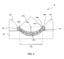
- FIG.2 shows a cross-sectional view (i.e. cross-sectional view along the A-A line in FIG.5 ) perpendicular to the drawing direction of the linear banks of organic EL element 10 having a concavely curved hole injection layer. Further, in FIG.2 , the anode and the organic light emitting layer are omitted. As shown in FIG.2 , organic EL element 10 has substrate 101, anode 103, concavely curved hole injection layer 105 and bank 107.
- bank 107 preferably has a forward-tapered shape in the case where the hole injection layer is concavely curved.
- the taper angle of bank 107 is 20 to 90°, and, more preferably, 40 to 70°.
- Tilt angle 105a of tangent line 1051 at edge 105e of concavely curved hole injection layer 105 is 20 to 90°, more preferably, 20 to 50°, and more preferably, the same extent to the taper angle of bank 107 (40 to 50°) as measured when concavely curved hole injection layer 105 is seen from a cross-section perpendicular to the drawing direction of linear banks 107.
- depth 105d of concavely curved hole injection layer 105 is preferably 50 to 300 nm.
- the depth of the concavely curved hole injection layer means a distance between most dented point 105b in the surface of concavely curved hole injection layer 105 and the line linked between edges 105e of hole injection layer 105.
- Curvature radius 105r of concavely curved hole injection layer 105 is preferably 10 to 300 ⁇ m, and, more preferably, 60 to 80 ⁇ m.
- the thickness of the organic light emitting layer (described later) is made uniform.
- the organic light emitting layer contains an organic light emitting material.
- the organic light emitting layer is provided on the hole injection layer in the region defined by the banks.
- the thickness of the organic light emitting layer is preferably approximately 50 to 100 nm (e.g. 70 nm).
- the organic light emitting layer is arranged in the region defined by the banks. That is, the organic light emitting layer is formed linearly inside the linear region. Therefore, the organic EL elements in one linear region share one organic light emitting layer.
- the organic light emitting material contained in the organic light emitting layer may be a small molecular organic light emitting material or an organic light emitting polymer material, and is preferably an organic light emitting polymer material. This is because the organic light emitting layer containing an organic light emitting polymer material can be formed easily with coating method.
- Examples of an organic light emitting polymer material include polyphenylenevinylene and its derivatives, polyphenylene and its derivatives, polyparaphenylene ethylene and its derivatives, poly-3-hexylthiophene (P3HT) and its derivatives, and polyfluorene (PF) and its derivatives.
- the organic light emitting material is selected as appropriate so that a desired color (red, green, or blue) is generated from each sub pixel (organic EL element).
- a desired color red, green, or blue
- the green sub pixel is arranged next to the red sub pixel
- the blue sub pixel is arranged next to the green sub pixel
- a red sub pixel is arranged next to the blue sub pixel.
- the organic light emitting layer often becomes concavely curved or convexly curved.
- the organic light emitting layer preferably becomes concavely curved.
- the physical properties of the ink having influence on the shape of the organic light emitting layer include, for example, the boiling point of the solvent and the concentration of the organic light emitting material.
- the shape of the hole injection layer is selected as appropriate depending on shape of the organic light emitting layer.
- the hole injection layer in the case where the organic light emitting layer is made concavely curved, the hole injection layer may be concavely curved, and, in the case where the organic light emitting layer is made convexly curved, the hole injection layer may be convexly curved.
- the interlayer may be set between the hole injection layer and the organic light emitting layer.
- the interlayer has a role of blocking intrusion of electrons into the hole injection layer and a role of efficiently transporting holes to the organic light emitting layer, and is made of a polyaniline material, for example.
- the interlayer is provided in the region defined by the banks. That is, the interlayer is formed linearly inside the linear region. Therefore, the organic EL elements in the linear region share one linear interlayer.
- the thickness of the interlayer is usually between 5 nm and 100 nm inclusive and is preferably between 10 nm and 50 nm inclusive (e.g. approximately 20 nm). Further, the interlayer may be omitted as long as holes are efficiently transported from the hole injection layer to the organic light emitting layer.
- the cathode is provided on the organic light emitting layer.
- the material of the cathode varies depending on whether the organic EL display panel of the present invention is of a bottom emission type or a top emission type.
- the cathode is required to be optically transparent. Therefore, examples of the material of the cathode include ITO, IZO, Ba, AI, WOx and so on.
- an organic buffer layer formed with the deposition method may be provided between the organic light emitting layer and the cathode.
- the material of the cathode is not particularly limited, and, for example, Ba, BaO, and Al.
- the organic EL display panel is an active matrix type
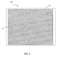
- all the organic EL elements may share one cathode (see FIG.4 ), because each sub pixel is driven by separate TFTs in an active matrix type organic EL display panel.
- the organic EL display panel is a passive matrix type
- a plurality of linear cathodes are arranged on the panel.
- the linear banks can function as a cathode separator.
- the drawing direction of the linear cathodes preferably crosses the drawing direction of the linear anodes at right angles.
- the organic EL display panel may be sealed by providing a cover material (sealing material) on the cathode.
- a cover material sealing material
- an organic EL element has an organic light emitting layer with uniform thickness, so that the light emitting area in the organic light emitting layer is large. Consequently, the organic EL display panel of the present invention has a high aperture ratio. Further, by making the thickness of the organic light emitting layer uniform, the organic light emitting layer will be deteriorated little. Therefore, the duration of the organic EL display panel of the present invention is long.
- the organic EL display panel of the present invention may be manufactured by any method as long as the effect of the present invention is not impaired.
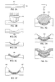
- the preferable manufacturing method of the organic EL display panel includes, for example: (1) the first step of providing a substrate ( FIG.3A ); (2) a second step of forming two or more concavely curved parts or convexly curved parts ( FIGS.3B and 3C ); (3) a third step of forming an anode on the concavely curved part or convexly curved part on the substrate ( FIG.3D ); (4) a fourth step of forming a concavely curved or convexly curved hole injection layer on the anode ( FIG.3E ); (5) a fifth step of forming linear banks ( FIG.3F ); (6) a sixth step of applying an ink containing an organic light emitting material in the region defined by the banks (i.e. linear region) to form an organic light emitting layer ( FIGS.3G and 3H ); and (7) a seventh step of forming a cathode on the organic light emitting layer ( FIG.3I ).
- the substrate may be directly subjected to wet etching or dry etching, or a photosensitive resin layer may be exposed and developed, which is laminated on the substrate surface which is formed to be the concavely curved parts or the convexly curved parts.
- a photosensitive resin layer may be exposed and developed, which is laminated on the substrate surface which is formed to be the concavely curved parts or the convexly curved parts.
- FIG.3A shows the first step.
- substrate 101 is provided.
- Substrate 101 has photosensitive resin layer 101'.
- Substrate 101 may have built-in driving TFTs.
- FIG.3B and 3C show the second step.
- concavely curved part 102 is formed on substrate 101.
- a positive photoresist is selected as the material of photosensitive resin layer 101' of substrate 101, and, photosensitive resin layer 101' may be exposed using mesh mask 113 in which the opening ratio near the center is higher than the opening ratio near the periphery, as shown in FIG.3B .
- mesh mask 113 in which the opening ratio near the center is higher than the opening ratio near the periphery
- FIG.3D shows the third step.
- anode 103 is formed on concavely curved part 102 on substrate 101.
- Anode 103 may be formed by forming a film made of the materials of anode 103 on concavely curved part 102 on substrate 101 with sputtering or the like, and by patterning the formed layer with etching.
- FIG.3E shows the fourth step.
- hole injection layer 105 is formed on anode 103.
- Hole injection layer 105 is formed by forming a film made of the materials of hole injection layer 105 on concavely curved anode 103 with sputtering or the like and by patterning the layer with etching.
- hole injection layer 105 By forming hole injection layer 105 on concavely curved anode 103 with sputtering or the like as mentioned above, concavely curved hole injection layer 105 can be obtained.
- FIG.3F shows the fifth step.
- linear banks 107 are formed. Banks 107 may be formed with photolithography or printing technologies.
- Formation of banks using the photolithography technologies includes the steps of (a) forming film of a photosensitive resin composition containing a resin on substrate 101 and hole injection layer 105 (b) exposing and developing the film so as to expose at least part of hole injection layer 105.
- a film of a photosensitive resin composition containing a resin on substrate 101 and hole injection layer 105 is formed by, for example, applying a resin composition using spin-coating, forming a film made of the resin composition; and drying the film made of the resin composition.
- the drying condition is not particularly limited, and the films may be left for 2 to 3 minutes at 80 °C.
- hole injection layer 105 is exposed i n the linear region in which the ink containing the organic light emitting material (described later) is to be applied.
- the developed film is subjected to baking treatment.
- the condition of the baking treatment is not particularly limited, the temperature is approximately 200 °C or more and the time period is approximately one hour, for example.
- the printing technology a technique such as intaglio printing, relief printing or the like may be used to form a patterned resin film. If banks 107 are formed by intaglio printing or the like, other component members will be damaged little.
- the manufacturing method of the organic EL display panel of the present invention may include a step of forming an inorganic film between the fourth step and fifth step.
- the inorganic film is formed with inorganic material using the CVD method.
- the formed inorganic film may be subject to dry-etching with gas including SiF and CF 4 to be patterned.
- FIGS.3G and 3H show the sixth step.
- organic light emitting layer 109 is formed on hole injection layer 105.
- Organic light emitting layer 109 is formed by applying ink 108 containing an organic light emitting material and solvent to the region defined by banks 107 (i.e. linear region) ( FIG.3G ), and by drying the ink applied.
- the solvent include an aromatic system solvent, for example, anisole.
- the applying means is not particularly limited. Examples of the applying means include ink-jet, dispenser, nozzle coating, spin coating intaglio printing, relief printing or the like.
- the preferable applying means is ink-jet.
- Organic light emitting layer 109 formed by drying ink 108 becomes concavely curved. Therefore, when the region on which organic light emitting layer 109 is formed is flat, the thickness of organic light emitting layer 109 of each organic EL element 10 will become non-uniform (see FIG.1 ).
- hole injection layer 105 in the region in which organic light emitting layer 109 is formed is also concavely curved. Consequently, even if organic light emitting layer 109 becomes concavely curved, the thickness of organic light emitting layer 109 on hole injection layer 105 is uniform.
- the manufacturing method of the present invention may have a step of forming an interlayer between the fifth step and the sixth step.
- the interlayer is formed by applying ink containing the material of the interlayer and solvent to the region defined by the banks.
- FIG.3I shows the seventh step.
- cathode 111 is formed on organic light emitting layer 109.
- Cathode 111 is formed with, for example, the deposition method or sputtering.
- a seal film may be formed on the cathode to prevent moisture or oxygen from intruding into organic light emitting layer.
- the manufacturing method of the organic EL display panel of the present invention it is possible to make the thickness of the organic light emitting layer in the organic EL element uniform, so that the aperture ratio of the organic EL display panel improves and the light emission efficiency improves. Further, when the thickness of the organic light emitting layer is uniform, it is possible to extend the life of an organic EL display panel and reduce power consumption.
- Embodiment 1 an active matrix type organic EL display panel will be described.
- FIG.4 is a plan view of organic EL display panel in Embodiment 1. As shown in FIG.4 , organic EL display panel 100 has cathode 111 covering the entire panel.
- FIG.5 is a plan view of organic EL display panel 100 omitting cathode 111.
- organic EL display panel 100 has linear banks 107 aligned in parallel to each other on substrate 101. Linear banks 107 define linear regions 11. A plurality of organic EL elements 10 are aligned in one row in linear region 11.
- Organic light emitting layer 109 is arranged linearly in linear region 11.
- Organic EL elements 10 aligned in linear region 11 share linear organic light emitting layer 109.
- Organic EL elements 10 aligned in linear region 11R emit red light
- organic EL elements 10 aligned in linear region 11G emit green light
- organic EL elements 10 aligned in linear region 11B emit blue light.
- Linear regions 11 are each defined by the banks, and therefore the inks applied in the regions will not become mixed. Further, by forming the organic light emitting layer linearly, the thickness of the organic light emitting layer becomes uniform in the linear direction.
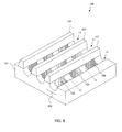
- FIG.6 is a perspective view of organic EL display panel 100 omitting cathode 111, organic light emitting layer 109 and interlayer 104 from organic EL display panel shown in FIG.5 .
- substrate 101 has convexly curved parts 102 in the shape of a parabolic cylinder.
- Anode 103 and hole injection layer 105 are formed on concavely curved part 102, so that, in the present embodiment, hole injection layer 105 is concavely curved, and the surface of hole injection layer 105 contacting the organic light emitting layer has a shape of a parabolic cylinder.
- the surface of region 12 between the organic EL elements has a shape of a parabolic cylinder.
- region 12 between the organic EL elements By making region 12 between the organic EL elements concavely curved, even when foreign substances such as particles are intruded on region 12 before forming the organic light emitting layer, it is possible to hold foreign substances in region 12 and prevent foreign substances from intruding on organic EL element.
- the organic EL element included in organic EL display panel 100 of Embodiment 1 will be described in detail.
- FIG.7 shows organic EL element 10 of cross-sectional view of organic EL display panel 100 along A-A line shown in FIG.5 .
- Organic EL element 10 has substrate 101, anode 103, hole injection layer 105, banks 107, interlayer 104 and organic light emitting layer 109.
- Substrate 101 has built-in driving TFTs.
- Substrate 101 has gate electrode 201, source electrode 203 and drain electrode 205.
- Gate insulating film 211 insulates gate electrode 201 from source electrode 203 and drain electrode 205.
- Channel 207 connects source electrode 203 and drain electrode 205.
- flattening film 213 is placed over channel 207, source electrode 203 and drain electrode 205. Drain electrode 205 and anode 103 are connected via contact hole 209.
- anode 103 and hole injection layer 105 is concavely curved.
- hole injection layer 105 concavely curved as mentioned above, the thickness of interlayer 104 and organic light emitting layer 109 formed on hole injection layer with coating method 105 becomes uniform.
- the thickness of organic light emitting layer is uniform. Further, it is possible to reduce the decrease of the yield caused by particles.
- Embodiment 1 the case is explained where the surface of the concavely curved hole injection layer has a shape of a parabolic cylinder.
- Embodiment 2 a case will be explained with an example where the surface of concavely curved the hole injection layer has a shape of an elliptical paraboloid.
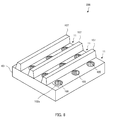
- FIG.8 is a perspective view of organic EL display panel 200 of Embodiment 2 omitting the cathode, the organic light emitting layer and the interlayer.
- Organic EL display panel 200 is the same as organic EL display panel 100 except the shape of concavely curved part 102a substrate 101 has. Therefore, the same reference numerals are assigned to the same components as in organic EL display panel 100 and the explanation thereof will be omitted.
- substrate 101 has concavely curved parts 102a aligned in a row in linear region 11.
- the surface of concavely curved part 102a has a shape of an elliptical paraboloid.
- each organic EL element is formed on concavely curved part 102a. Therefore, the hole injection layer of each organic EL element is concavely curved and the surface of the hole injection layer has a shape of an elliptical paraboloid.
- each surface of the concavely curved hole injection layer has a shape of an elliptical paraboloid, so that it is possible to make the thickness of the organic light emitting layer uniform and improve the aperture ratio.
- Embodiments 1 and 2 examples where the bank has a one-layered structure are explained.
- Embodiment 3 an example where the bank has a two-layered structure will be explained.
- a plane view of the organic EL display panel of Embodiment 3 is the same as of organic EL display panel 100 shown in FIGS.4 and 5 of Embodiment 1.
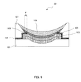
- FIG.9 is a cross-sectional view of organic EL element 20 included in organic EL display panel of Embodiment 3.
- Organic EL element 20 is the same as organic EL element 10 other than having an inorganic film. Therefore, the same reference numerals are assigned to the same components as in organic EL element 10 and the explanation thereof will be omitted.
- organic EL element 20 has inorganic film 106 placed under bank 107.
- Inorganic film 106 is placed on substrate 101 such that inorganic film cover the end of hole injection layer 105. Further, inorganic film 106 protrudes from bank 107 into the region defined by banks 107. The width d of inorganic film 106 protruded from banks 107 is 1 to 10 ⁇ m.
- inorganic film protrude from an organic layer into the linear region it is possible to prevent the dust produced during the process of forming the organic layer from adhering to a hole injection layer. As a result, it is possible to make the thickness of layers piled over an anode uniform, so that the light emission efficiency of the organic EL display panel improves substantially.
- Embodiments 1 to 3 examples where the hole injection layer is concavely curved are explained.
- Embodiment 4 an example where the hole injection layer is convexly curved will be explained. That is, a case will explained where the organic light emitting layer becomes convexly curved.
- a plan view of the organic EL display panel of Embodiment 4 is the same as of organic EL display panel 100 shown in FIGS.4 and 5 of Embodiment 1.
- FIG.10 is a cross-sectional view of organic EL element 30 included in organic EL display panel of Embodiment 4.
- organic EL element 30 has substrate 101, anode 103, hole injection layer 105, banks 107, interlayer 104 and organic light emitting layer 109.
- a feature of the present embodiment includes that anode 103 and hole injection layer 105 are convexly curved. Further, substrate 101 has convexly curved part 102'.
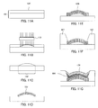
- FIG.11 shows a manufacturing process of organic EL display panel in Embodiment 4.
- the manufacturing method of the organic EL display panel in Embodiment 4 includes: ( 1) the first step of providing substrate 101 ( FIG.11A ); (2) a second step of forming convexly curved part 102' on substrate 101 ( FIGS.11B and 11C ); (3) a third step of forming anode 103 on convexly curved part 102' on substrate 101 ( FIG.11D ); (4) a fourth step of forming convexly curved hole injection layer 105 on anode 103 ( FIG.11E ); (5) a fifth step of forming banks 107 ( FIG.11F ); and ( 6 ) a sixth step of forming interlayer 104 and organic light emitting layer 109 inside the region defined by banks 107 ( FIGS.11G ).
- the organic EL display panel of the present invention is applicable to, for example, organic EL displays (e.g. large screen televisions and monitors of information equipments including mobile phones).
Landscapes
- Engineering & Computer Science (AREA)
- Physics & Mathematics (AREA)
- Optics & Photonics (AREA)
- Microelectronics & Electronic Packaging (AREA)
- Manufacturing & Machinery (AREA)
- Electroluminescent Light Sources (AREA)
- Devices For Indicating Variable Information By Combining Individual Elements (AREA)
Applications Claiming Priority (2)
| Application Number | Priority Date | Filing Date | Title |
|---|---|---|---|
| JP2008047043 | 2008-02-28 | ||
| PCT/JP2009/000366 WO2009107323A1 (ja) | 2008-02-28 | 2009-01-30 | 有機elディスプレイパネル |
Publications (3)
| Publication Number | Publication Date |
|---|---|
| EP2270896A1 true EP2270896A1 (de) | 2011-01-05 |
| EP2270896A4 EP2270896A4 (de) | 2011-05-18 |
| EP2270896B1 EP2270896B1 (de) | 2014-12-24 |
Family
ID=41015730
Family Applications (1)
| Application Number | Title | Priority Date | Filing Date |
|---|---|---|---|
| EP09700056.6A Active EP2270896B1 (de) | 2008-02-28 | 2009-01-30 | Organische el-anzeigetafel |
Country Status (6)
| Country | Link |
|---|---|
| US (1) | US7812345B2 (de) |
| EP (1) | EP2270896B1 (de) |
| JP (2) | JP4418525B2 (de) |
| KR (1) | KR100959466B1 (de) |
| CN (1) | CN101681997B (de) |
| WO (1) | WO2009107323A1 (de) |
Cited By (8)
| Publication number | Priority date | Publication date | Assignee | Title |
|---|---|---|---|---|
| EP2398084A4 (de) * | 2009-02-10 | 2013-03-27 | Panasonic Corp | Lichtemittierendes element, lichtemittierende vorrichtung mit dem lichtemittierenden element sowie verfahren zur herstellung des lichtemittierenden elements |
| US8852977B2 (en) | 2010-08-06 | 2014-10-07 | Panasonic Corporation | Method for producing light-emitting elements |
| US8890129B2 (en) | 2010-08-06 | 2014-11-18 | Panasonic Corporation | Light emitting device, light emitting apparatus provided with a light emitting device, and method of manufacturing a light emitting device |
| US8927976B2 (en) | 2010-08-06 | 2015-01-06 | Panasonic Corporation | Organic EL element and production method for same |
| US8999832B2 (en) | 2010-08-06 | 2015-04-07 | Panasonic Corporation | Organic EL element |
| US9130187B2 (en) | 2010-08-06 | 2015-09-08 | Joled Inc. | Organic EL element, display device, and light-emitting device |
| US9843010B2 (en) | 2010-08-06 | 2017-12-12 | Joled Inc. | Light-emitting element, light-emitting device provided with light-emitting element, and light-emitting element production method |
| EP2398083B1 (de) * | 2009-02-10 | 2018-06-13 | Joled Inc. | Lichtemittierendes element, anzeigevorrichtung und verfahren zur herstellung des lichtemittierenden elements |
Families Citing this family (70)
| Publication number | Priority date | Publication date | Assignee | Title |
|---|---|---|---|---|
| KR101480005B1 (ko) * | 2008-02-25 | 2015-01-08 | 삼성디스플레이 주식회사 | 유기 발광 표시 장치 및 그 제조 방법 |
| US8242516B2 (en) * | 2008-08-29 | 2012-08-14 | Panasonic Corporation | Organic EL display panel and method of manufacturing the same |
| AT507322B1 (de) * | 2008-10-07 | 2011-07-15 | Nanoident Technologies Ag | Schaltvorrichtung zur elektrischen kontaktprüfung |
| CN102308671B (zh) | 2009-02-10 | 2015-01-21 | 松下电器产业株式会社 | 发光元件的制造方法和发光元件、以及发光装置的制造方法和发光装置 |
| JP5437736B2 (ja) | 2009-08-19 | 2014-03-12 | パナソニック株式会社 | 有機el素子 |
| WO2011040237A1 (ja) * | 2009-09-30 | 2011-04-07 | 凸版印刷株式会社 | 有機エレクトロルミネセンス素子、有機エレクトロルミネセンスディスプレイパネルおよび有機エレクトロルミネセンスディスプレイパネル製造方法 |
| JP5209123B2 (ja) | 2009-11-04 | 2013-06-12 | パナソニック株式会社 | 表示パネル装置及びその製造方法 |
| KR101546552B1 (ko) * | 2009-11-11 | 2015-08-21 | 가부시키가이샤 제이올레드 | 유기 el 소자 및 그 제조 방법 |
| WO2011161727A1 (ja) | 2010-06-24 | 2011-12-29 | パナソニック株式会社 | 有機el素子の製造方法、表示装置、発光装置および紫外光照射装置 |
| CN102473847B (zh) | 2010-06-24 | 2015-01-14 | 松下电器产业株式会社 | 有机el元件、显示装置以及发光装置 |
| JP5330545B2 (ja) * | 2010-07-05 | 2013-10-30 | パナソニック株式会社 | 発光素子の製造方法 |
| JP5524954B2 (ja) * | 2010-07-05 | 2014-06-18 | パナソニック株式会社 | 有機el表示パネルとその製造方法 |
| JP5624141B2 (ja) | 2010-07-30 | 2014-11-12 | パナソニック株式会社 | 有機el素子 |
| WO2012017490A1 (ja) * | 2010-08-06 | 2012-02-09 | パナソニック株式会社 | 有機el素子、表示装置および発光装置 |
| WO2012017503A1 (ja) * | 2010-08-06 | 2012-02-09 | パナソニック株式会社 | 有機el素子 |
| JP5658256B2 (ja) * | 2010-08-06 | 2015-01-21 | パナソニック株式会社 | 発光素子とその製造方法、および発光装置 |
| JP5620494B2 (ja) | 2010-08-06 | 2014-11-05 | パナソニック株式会社 | 発光素子、表示装置、および発光素子の製造方法 |
| WO2012017502A1 (ja) * | 2010-08-06 | 2012-02-09 | パナソニック株式会社 | 有機el素子およびその製造方法 |
| JP5574456B2 (ja) | 2010-08-06 | 2014-08-20 | パナソニック株式会社 | 発光素子とその製造方法、および発光装置 |
| WO2012017485A1 (ja) * | 2010-08-06 | 2012-02-09 | パナソニック株式会社 | 有機el素子、表示装置および発光装置 |
| WO2012017501A1 (ja) | 2010-08-06 | 2012-02-09 | パナソニック株式会社 | 有機el素子およびその製造方法 |
| WO2012017499A1 (ja) * | 2010-08-06 | 2012-02-09 | パナソニック株式会社 | 有機el素子 |
| CN102960065B (zh) * | 2010-08-25 | 2016-03-16 | 株式会社日本有机雷特显示器 | 有机发光元件及其制造方法以及有机显示面板和有机显示装置 |
| JP5276222B2 (ja) * | 2010-08-25 | 2013-08-28 | パナソニック株式会社 | 有機発光素子とその製造方法、および有機表示パネルと有機表示装置 |
| JP5606227B2 (ja) * | 2010-09-10 | 2014-10-15 | 株式会社日本触媒 | 自己組織化単分子膜を有する有機薄膜電界発光素子 |
| US9182146B2 (en) | 2010-10-01 | 2015-11-10 | Tokyo Institute Of Technology | Cross linear type solar heat collecting apparatus |
| JP5573616B2 (ja) * | 2010-11-12 | 2014-08-20 | 住友化学株式会社 | 表示装置 |
| JP5676652B2 (ja) | 2011-01-21 | 2015-02-25 | パナソニック株式会社 | 有機el素子 |
| CN103314462B (zh) | 2011-02-23 | 2016-03-02 | 株式会社日本有机雷特显示器 | 有机el显示面板和有机el显示装置 |
| JP5809234B2 (ja) | 2011-02-25 | 2015-11-10 | 株式会社Joled | 有機el表示パネルおよび有機el表示装置 |
| TW201219543A (en) * | 2011-04-01 | 2012-05-16 | Chi Mei Corp | having the formula of Ii-Mm-Aa-Bb-Ot-Nn:Zr and providing the high luminance and durability |
| CN102884650A (zh) | 2011-05-11 | 2013-01-16 | 松下电器产业株式会社 | 有机el显示面板及有机el显示装置 |
| JP5861210B2 (ja) * | 2011-07-15 | 2016-02-16 | 株式会社Joled | 有機発光素子 |
| CN104247071B (zh) * | 2012-06-01 | 2016-08-17 | 株式会社日本有机雷特显示器 | 有机发光元件、有机el显示面板、有机el显示装置、和涂敷型器件、以及它们的制造方法 |
| KR101941178B1 (ko) * | 2012-09-28 | 2019-01-23 | 삼성디스플레이 주식회사 | 유기 발광 표시 장치 및 유기 발광 표시 장치의 제조 방법 |
| US20140346468A1 (en) * | 2013-05-27 | 2014-11-27 | Samsung Display Co., Ltd. | Organic light emitting display device having a channel in pixel defining layer |
| JP2015050022A (ja) * | 2013-08-30 | 2015-03-16 | 株式会社ジャパンディスプレイ | 有機el表示装置 |
| CN103943787B (zh) * | 2014-03-28 | 2016-08-24 | 京东方科技集团股份有限公司 | 一种oled显示器及其制备方法 |
| CN103928626A (zh) * | 2014-04-17 | 2014-07-16 | 上海和辉光电有限公司 | Oled发光装置及其制造方法 |
| CN104103673B (zh) * | 2014-07-09 | 2017-06-20 | 京东方科技集团股份有限公司 | 一种oled显示器及其制备方法 |
| CN104362257B (zh) * | 2014-10-22 | 2017-10-17 | 京东方科技集团股份有限公司 | 一种顶发射oled器件及其制作方法、显示设备 |
| KR101664007B1 (ko) | 2014-12-31 | 2016-10-11 | 엘지디스플레이 주식회사 | 유기발광표시장치 및 그 제조방법 |
| CN104698662A (zh) * | 2015-03-26 | 2015-06-10 | 京东方科技集团股份有限公司 | 显示装置及其制作方法 |
| CN104779268B (zh) * | 2015-04-13 | 2016-07-06 | 深圳市华星光电技术有限公司 | Oled显示器件 |
| KR102513510B1 (ko) * | 2015-05-28 | 2023-03-22 | 엘지디스플레이 주식회사 | 유기발광 표시장치 |
| KR102467214B1 (ko) * | 2015-09-14 | 2022-11-14 | 엘지디스플레이 주식회사 | 유기발광다이오드표시장치 및 이의 제조방법 |
| KR20170080459A (ko) * | 2015-12-30 | 2017-07-10 | 엘지디스플레이 주식회사 | 유기발광다이오드표시장치 |
| CN105576145B (zh) * | 2016-02-29 | 2018-11-30 | Tcl集团股份有限公司 | 一种量子点发光二极管、显示器以及制备方法 |
| CN105826356B (zh) * | 2016-05-04 | 2020-05-05 | Tcl科技集团股份有限公司 | 一种高开口率的显示面板及其制作方法 |
| CN106783929B (zh) * | 2016-12-29 | 2020-08-11 | 上海天马微电子有限公司 | 一种显示面板、显示设备 |
| CN107316949B (zh) * | 2017-07-11 | 2020-07-31 | 京东方科技集团股份有限公司 | 显示面板及其制造方法、显示装置 |
| CN107403811A (zh) * | 2017-09-07 | 2017-11-28 | 京东方科技集团股份有限公司 | 显示基板及其制造方法和显示装置 |
| JP7027141B2 (ja) * | 2017-12-05 | 2022-03-01 | キヤノン株式会社 | トップエミッション型有機el素子、トップエミッション型有機el装置、およびトップエミッション型有機el素子の製造方法 |
| CN108400153B (zh) * | 2018-04-03 | 2021-01-26 | 京东方科技集团股份有限公司 | 一种oled基板及其制备方法、显示装置 |
| CN110098221A (zh) * | 2018-05-29 | 2019-08-06 | 广东聚华印刷显示技术有限公司 | 像素结构及其制备方法、显示屏和显示装置 |
| JP6807350B2 (ja) * | 2018-05-30 | 2021-01-06 | 株式会社Joled | 有機el表示パネル、有機el表示装置、及び、有機el表示パネルの製造方法 |
| CN109979983B (zh) | 2018-06-22 | 2021-05-28 | 友达光电股份有限公司 | 有机发光二极管显示装置 |
| KR102724703B1 (ko) * | 2018-10-23 | 2024-11-01 | 삼성디스플레이 주식회사 | 디스플레이 장치 및 디스플레이 장치를 제조하기 위한 마스크 |
| CN109935726B (zh) * | 2019-03-19 | 2020-12-08 | 京东方科技集团股份有限公司 | 有机发光显示面板、其制造方法及显示装置 |
| CN110148685B (zh) * | 2019-05-07 | 2021-01-15 | 深圳市华星光电半导体显示技术有限公司 | 显示面板及其制作方法 |
| CN110797473B (zh) * | 2019-11-12 | 2022-10-28 | 京东方科技集团股份有限公司 | 一种显示基板、显示基板的制备方法及显示面板 |
| KR102745536B1 (ko) * | 2019-12-13 | 2024-12-24 | 엘지디스플레이 주식회사 | 표시 장치 |
| CN111312791B (zh) * | 2020-03-02 | 2022-12-09 | 京东方科技集团股份有限公司 | 显示面板、其制作方法及显示装置 |
| CN111710694B (zh) * | 2020-05-28 | 2022-10-25 | 京东方科技集团股份有限公司 | 显示基板及其制作方法、显示装置 |
| KR102907280B1 (ko) | 2020-09-11 | 2026-01-05 | 삼성디스플레이 주식회사 | 전자 장치 |
| CN112349872A (zh) * | 2020-11-05 | 2021-02-09 | 合肥京东方卓印科技有限公司 | 一种显示屏的封装方法、显示屏及电子设备 |
| KR20220089180A (ko) * | 2020-12-21 | 2022-06-28 | 엘지디스플레이 주식회사 | 발광 표시 장치 |
| CN112952025A (zh) * | 2021-03-31 | 2021-06-11 | 京东方科技集团股份有限公司 | 显示基板及显示装置 |
| CN114203773A (zh) * | 2021-11-16 | 2022-03-18 | 长沙惠科光电有限公司 | 像素结构及其制备方法和显示面板 |
| CN114975821A (zh) * | 2022-05-05 | 2022-08-30 | 武汉华星光电半导体显示技术有限公司 | 显示面板及其制作方法、和显示装置 |
Family Cites Families (34)
| Publication number | Priority date | Publication date | Assignee | Title |
|---|---|---|---|---|
| JPH0547470A (ja) | 1991-08-20 | 1993-02-26 | Matsushita Electric Ind Co Ltd | 分散型elおよびその製造法 |
| JPH10208875A (ja) | 1997-01-27 | 1998-08-07 | Hokuriku Electric Ind Co Ltd | 有機el素子とその製造方法 |
| JPH10223368A (ja) | 1997-01-31 | 1998-08-21 | Hokuriku Electric Ind Co Ltd | 有機el素子とその製造方法 |
| JP3783558B2 (ja) | 2000-11-30 | 2006-06-07 | 松下電工株式会社 | モジュラコネクタ |
| JP2002170663A (ja) * | 2000-12-04 | 2002-06-14 | Canon Inc | 有機発光素子及びその製造方法 |
| JP2003264084A (ja) | 2002-03-11 | 2003-09-19 | Harison Toshiba Lighting Corp | 発光装置 |
| US20050062412A1 (en) | 2001-10-25 | 2005-03-24 | Yoshio Taniguchi | Light emitting apparatus |
| JP2004047215A (ja) | 2002-07-10 | 2004-02-12 | Toshiba Corp | 有機el素子および有機el表示装置 |
| GB2416066B (en) * | 2002-07-31 | 2006-04-12 | Dainippon Printing Co Ltd | Electroluminescent display and process for producing the same |
| JP3956046B2 (ja) | 2002-09-30 | 2007-08-08 | 株式会社豊田自動織機 | El装置及びその製造方法並びにel装置を用いた液晶表示装置 |
| JP2004234901A (ja) * | 2003-01-28 | 2004-08-19 | Seiko Epson Corp | ディスプレイ基板、有機el表示装置、ディスプレイ基板の製造方法および電子機器 |
| JP4702516B2 (ja) | 2003-05-07 | 2011-06-15 | エルジー エレクトロニクス インコーポレイティド | 有機el素子及びその製造方法 |
| JP2005012173A (ja) * | 2003-05-28 | 2005-01-13 | Seiko Epson Corp | 膜パターン形成方法、デバイス及びデバイスの製造方法、電気光学装置、並びに電子機器 |
| JP4344270B2 (ja) * | 2003-05-30 | 2009-10-14 | セイコーエプソン株式会社 | 液晶表示装置の製造方法 |
| JP2005013986A (ja) * | 2003-05-30 | 2005-01-20 | Seiko Epson Corp | デバイスとその製造方法、アクティブマトリクス基板の製造方法及び電気光学装置並びに電子機器 |
| JP3750682B2 (ja) * | 2003-06-26 | 2006-03-01 | セイコーエプソン株式会社 | 有機el装置とその製造方法、並びに電子機器 |
| JP4049033B2 (ja) * | 2003-06-26 | 2008-02-20 | セイコーエプソン株式会社 | 有機el装置とその製造方法 |
| WO2005025276A1 (en) | 2003-09-08 | 2005-03-17 | Lg Chem, Ltd. | Highly efficient organic light emitting device using substrate having nanosized hemispherical recesses and method for preparing the same |
| TWI315162B (en) | 2003-12-08 | 2009-09-21 | Chi Mei Optoelectronics Corporatio | Organic electroluminescent device |
| JP2005174717A (ja) | 2003-12-10 | 2005-06-30 | Samsung Yokohama Research Institute Co Ltd | 有機el素子及びその製造方法 |
| US20050174041A1 (en) | 2004-02-05 | 2005-08-11 | Au Optronics | Display device with improved light emitting diode and a method of manufacturing the improved light emitting diode |
| CN100525558C (zh) | 2004-04-30 | 2009-08-05 | 三洋电机株式会社 | 发光显示器 |
| JP4645064B2 (ja) * | 2004-05-19 | 2011-03-09 | セイコーエプソン株式会社 | 電気光学装置の製造方法 |
| JP4525536B2 (ja) * | 2004-11-22 | 2010-08-18 | セイコーエプソン株式会社 | El装置および電子機器 |
| JP2006253443A (ja) * | 2005-03-11 | 2006-09-21 | Seiko Epson Corp | 有機el装置、その製造方法および電子機器 |
| JP4682651B2 (ja) | 2005-03-11 | 2011-05-11 | セイコーエプソン株式会社 | エレクトロルミネッセンス装置、電子機器 |
| JP4106076B2 (ja) | 2005-09-29 | 2008-06-25 | 松下電器産業株式会社 | 有機elディスプレイおよびその製造方法 |
| JP5256605B2 (ja) * | 2006-01-18 | 2013-08-07 | 凸版印刷株式会社 | 有機エレクトロルミネッセンス素子の製造方法 |
| JP2007288074A (ja) * | 2006-04-19 | 2007-11-01 | Matsushita Electric Ind Co Ltd | 有機エレクトロルミネッセント素子およびその製造方法 |
| US20070241665A1 (en) | 2006-04-12 | 2007-10-18 | Matsushita Electric Industrial Co., Ltd. | Organic electroluminescent element, and manufacturing method thereof, as well as display device and exposure apparatus using the same |
| US20070290604A1 (en) | 2006-06-16 | 2007-12-20 | Matsushita Electric Industrial Co., Ltd. | Organic electroluminescent device and method of producing the same |
| JP2007335737A (ja) | 2006-06-16 | 2007-12-27 | Matsushita Electric Ind Co Ltd | 有機エレクトロルミネッセント素子およびその製造方法 |
| JP2008243773A (ja) * | 2007-03-29 | 2008-10-09 | Seiko Epson Corp | 電気発光装置、その製造方法、電子機器、薄膜構造体、薄膜形成方法 |
| US8017940B2 (en) | 2007-05-25 | 2011-09-13 | Panasonic Corporation | Organic transistor, method of forming organic transistor and organic EL display with organic transistor |
-
2009
- 2009-01-30 JP JP2009516774A patent/JP4418525B2/ja active Active
- 2009-01-30 KR KR1020097012715A patent/KR100959466B1/ko not_active Expired - Fee Related
- 2009-01-30 WO PCT/JP2009/000366 patent/WO2009107323A1/ja not_active Ceased
- 2009-01-30 US US12/521,044 patent/US7812345B2/en active Active
- 2009-01-30 CN CN2009800000579A patent/CN101681997B/zh active Active
- 2009-01-30 EP EP09700056.6A patent/EP2270896B1/de active Active
- 2009-11-26 JP JP2009269112A patent/JP4526595B2/ja active Active
Cited By (10)
| Publication number | Priority date | Publication date | Assignee | Title |
|---|---|---|---|---|
| EP2398084A4 (de) * | 2009-02-10 | 2013-03-27 | Panasonic Corp | Lichtemittierendes element, lichtemittierende vorrichtung mit dem lichtemittierenden element sowie verfahren zur herstellung des lichtemittierenden elements |
| US8866160B2 (en) | 2009-02-10 | 2014-10-21 | Panasonic Corporation | Light-emitting element, device, and manufacturing method including a charge injection layer having a recess for suppressing uneven luminance |
| EP2398083B1 (de) * | 2009-02-10 | 2018-06-13 | Joled Inc. | Lichtemittierendes element, anzeigevorrichtung und verfahren zur herstellung des lichtemittierenden elements |
| EP2398085B1 (de) * | 2009-02-10 | 2018-06-27 | Joled Inc. | Lichtemittierendes element, anzeigevorrichtung und verfahren zur herstellung des lichtemittierenden elements |
| US8852977B2 (en) | 2010-08-06 | 2014-10-07 | Panasonic Corporation | Method for producing light-emitting elements |
| US8890129B2 (en) | 2010-08-06 | 2014-11-18 | Panasonic Corporation | Light emitting device, light emitting apparatus provided with a light emitting device, and method of manufacturing a light emitting device |
| US8927976B2 (en) | 2010-08-06 | 2015-01-06 | Panasonic Corporation | Organic EL element and production method for same |
| US8999832B2 (en) | 2010-08-06 | 2015-04-07 | Panasonic Corporation | Organic EL element |
| US9130187B2 (en) | 2010-08-06 | 2015-09-08 | Joled Inc. | Organic EL element, display device, and light-emitting device |
| US9843010B2 (en) | 2010-08-06 | 2017-12-12 | Joled Inc. | Light-emitting element, light-emitting device provided with light-emitting element, and light-emitting element production method |
Also Published As
| Publication number | Publication date |
|---|---|
| JP2010050107A (ja) | 2010-03-04 |
| KR20090121272A (ko) | 2009-11-25 |
| EP2270896A4 (de) | 2011-05-18 |
| KR100959466B1 (ko) | 2010-05-25 |
| US7812345B2 (en) | 2010-10-12 |
| WO2009107323A1 (ja) | 2009-09-03 |
| EP2270896B1 (de) | 2014-12-24 |
| CN101681997B (zh) | 2011-06-01 |
| JP4526595B2 (ja) | 2010-08-18 |
| US20100181554A1 (en) | 2010-07-22 |
| CN101681997A (zh) | 2010-03-24 |
| JP4418525B2 (ja) | 2010-02-17 |
| JPWO2009107323A1 (ja) | 2011-06-30 |
Similar Documents
| Publication | Publication Date | Title |
|---|---|---|
| US7812345B2 (en) | Organic EL display panel | |
| US7764014B2 (en) | Organic EL display panel with banks defining line-state pixels | |
| US7683537B2 (en) | Organic EL device and display | |
| US7888867B2 (en) | Organic el device having bank with groove, organic el display panel, and method for manufacturing the organic el device | |
| US8130177B2 (en) | Organic EL display panel and manufacturing method thereof | |
| KR100817992B1 (ko) | 표시장치 및 그 제조방법 | |
| US8570252B2 (en) | Organic EL light emitting device | |
| US9099408B2 (en) | Organic light-emitting diode (OLED) display | |
| JP2005203215A (ja) | 有機el素子 | |
| US20090322210A1 (en) | Organic electroluminescent element substrate, and organic electroluminescent element and the manufacturing method | |
| US7449252B2 (en) | Organic electroluminescent device, manufacturing method thereof, and electronic apparatus | |
| KR101608965B1 (ko) | 듀얼패널 타입 유기전계발광소자의 제조방법 |
Legal Events
| Date | Code | Title | Description |
|---|---|---|---|
| PUAI | Public reference made under article 153(3) epc to a published international application that has entered the european phase |
Free format text: ORIGINAL CODE: 0009012 |
|
| 17P | Request for examination filed |
Effective date: 20090618 |
|
| AK | Designated contracting states |
Kind code of ref document: A1 Designated state(s): AT BE BG CH CY CZ DE DK EE ES FI FR GB GR HR HU IE IS IT LI LT LU LV MC MK MT NL NO PL PT RO SE SI SK TR |
|
| AX | Request for extension of the european patent |
Extension state: AL BA RS |
|
| A4 | Supplementary search report drawn up and despatched |
Effective date: 20110415 |
|
| RIC1 | Information provided on ipc code assigned before grant |
Ipc: H05B 33/12 20060101ALI20110411BHEP Ipc: H01L 51/50 20060101AFI20090922BHEP Ipc: H05B 33/10 20060101ALI20110411BHEP Ipc: H01L 51/52 20060101ALI20110411BHEP Ipc: H01L 51/00 20060101ALI20110411BHEP Ipc: H05B 33/26 20060101ALI20110411BHEP |
|
| DAX | Request for extension of the european patent (deleted) | ||
| 17Q | First examination report despatched |
Effective date: 20130709 |
|
| REG | Reference to a national code |
Ref country code: DE Ref legal event code: R079 Ref document number: 602009028524 Country of ref document: DE Free format text: PREVIOUS MAIN CLASS: H01L0051500000 Ipc: H01L0027320000 |
|
| GRAP | Despatch of communication of intention to grant a patent |
Free format text: ORIGINAL CODE: EPIDOSNIGR1 |
|
| RIC1 | Information provided on ipc code assigned before grant |
Ipc: H01L 27/32 20060101AFI20140206BHEP |
|
| INTG | Intention to grant announced |
Effective date: 20140225 |
|
| GRAP | Despatch of communication of intention to grant a patent |
Free format text: ORIGINAL CODE: EPIDOSNIGR1 |
|
| INTG | Intention to grant announced |
Effective date: 20140718 |
|
| GRAS | Grant fee paid |
Free format text: ORIGINAL CODE: EPIDOSNIGR3 |
|
| GRAA | (expected) grant |
Free format text: ORIGINAL CODE: 0009210 |
|
| AK | Designated contracting states |
Kind code of ref document: B1 Designated state(s): AT BE BG CH CY CZ DE DK EE ES FI FR GB GR HR HU IE IS IT LI LT LU LV MC MK MT NL NO PL PT RO SE SI SK TR |
|
| REG | Reference to a national code |
Ref country code: GB Ref legal event code: FG4D |
|
| REG | Reference to a national code |
Ref country code: CH Ref legal event code: EP |
|
| REG | Reference to a national code |
Ref country code: IE Ref legal event code: FG4D |
|
| REG | Reference to a national code |
Ref country code: AT Ref legal event code: REF Ref document number: 703524 Country of ref document: AT Kind code of ref document: T Effective date: 20150115 |
|
| REG | Reference to a national code |
Ref country code: DE Ref legal event code: R096 Ref document number: 602009028524 Country of ref document: DE Effective date: 20150219 |
|
| REG | Reference to a national code |
Ref country code: DE Ref legal event code: R082 Ref document number: 602009028524 Country of ref document: DE Representative=s name: GRUENECKER PATENT- UND RECHTSANWAELTE PARTG MB, DE |
|
| REG | Reference to a national code |
Ref country code: NL Ref legal event code: VDEP Effective date: 20141224 |
|
| PG25 | Lapsed in a contracting state [announced via postgrant information from national office to epo] |
Ref country code: NO Free format text: LAPSE BECAUSE OF FAILURE TO SUBMIT A TRANSLATION OF THE DESCRIPTION OR TO PAY THE FEE WITHIN THE PRESCRIBED TIME-LIMIT Effective date: 20150324 Ref country code: FI Free format text: LAPSE BECAUSE OF FAILURE TO SUBMIT A TRANSLATION OF THE DESCRIPTION OR TO PAY THE FEE WITHIN THE PRESCRIBED TIME-LIMIT Effective date: 20141224 Ref country code: LT Free format text: LAPSE BECAUSE OF FAILURE TO SUBMIT A TRANSLATION OF THE DESCRIPTION OR TO PAY THE FEE WITHIN THE PRESCRIBED TIME-LIMIT Effective date: 20141224 |
|
| REG | Reference to a national code |
Ref country code: DE Ref legal event code: R081 Ref document number: 602009028524 Country of ref document: DE Owner name: JOLED, INC., JP Free format text: FORMER OWNER: PANASONIC CORPORATION, KADOMA-SHI, OSAKA, JP Effective date: 20150330 Ref country code: DE Ref legal event code: R082 Ref document number: 602009028524 Country of ref document: DE Representative=s name: GRUENECKER PATENT- UND RECHTSANWAELTE PARTG MB, DE Effective date: 20150330 |
|
| REG | Reference to a national code |
Ref country code: LT Ref legal event code: MG4D |
|
| PG25 | Lapsed in a contracting state [announced via postgrant information from national office to epo] |
Ref country code: LV Free format text: LAPSE BECAUSE OF FAILURE TO SUBMIT A TRANSLATION OF THE DESCRIPTION OR TO PAY THE FEE WITHIN THE PRESCRIBED TIME-LIMIT Effective date: 20141224 Ref country code: SE Free format text: LAPSE BECAUSE OF FAILURE TO SUBMIT A TRANSLATION OF THE DESCRIPTION OR TO PAY THE FEE WITHIN THE PRESCRIBED TIME-LIMIT Effective date: 20141224 Ref country code: GR Free format text: LAPSE BECAUSE OF FAILURE TO SUBMIT A TRANSLATION OF THE DESCRIPTION OR TO PAY THE FEE WITHIN THE PRESCRIBED TIME-LIMIT Effective date: 20150325 Ref country code: HR Free format text: LAPSE BECAUSE OF FAILURE TO SUBMIT A TRANSLATION OF THE DESCRIPTION OR TO PAY THE FEE WITHIN THE PRESCRIBED TIME-LIMIT Effective date: 20141224 |
|
| REG | Reference to a national code |
Ref country code: AT Ref legal event code: MK05 Ref document number: 703524 Country of ref document: AT Kind code of ref document: T Effective date: 20141224 |
|
| PG25 | Lapsed in a contracting state [announced via postgrant information from national office to epo] |
Ref country code: NL Free format text: LAPSE BECAUSE OF FAILURE TO SUBMIT A TRANSLATION OF THE DESCRIPTION OR TO PAY THE FEE WITHIN THE PRESCRIBED TIME-LIMIT Effective date: 20141224 |
|
| PG25 | Lapsed in a contracting state [announced via postgrant information from national office to epo] |
Ref country code: SK Free format text: LAPSE BECAUSE OF FAILURE TO SUBMIT A TRANSLATION OF THE DESCRIPTION OR TO PAY THE FEE WITHIN THE PRESCRIBED TIME-LIMIT Effective date: 20141224 Ref country code: CZ Free format text: LAPSE BECAUSE OF FAILURE TO SUBMIT A TRANSLATION OF THE DESCRIPTION OR TO PAY THE FEE WITHIN THE PRESCRIBED TIME-LIMIT Effective date: 20141224 Ref country code: EE Free format text: LAPSE BECAUSE OF FAILURE TO SUBMIT A TRANSLATION OF THE DESCRIPTION OR TO PAY THE FEE WITHIN THE PRESCRIBED TIME-LIMIT Effective date: 20141224 Ref country code: ES Free format text: LAPSE BECAUSE OF FAILURE TO SUBMIT A TRANSLATION OF THE DESCRIPTION OR TO PAY THE FEE WITHIN THE PRESCRIBED TIME-LIMIT Effective date: 20141224 Ref country code: RO Free format text: LAPSE BECAUSE OF FAILURE TO SUBMIT A TRANSLATION OF THE DESCRIPTION OR TO PAY THE FEE WITHIN THE PRESCRIBED TIME-LIMIT Effective date: 20141224 |
|
| REG | Reference to a national code |
Ref country code: CH Ref legal event code: PL |
|
| PG25 | Lapsed in a contracting state [announced via postgrant information from national office to epo] |
Ref country code: PL Free format text: LAPSE BECAUSE OF FAILURE TO SUBMIT A TRANSLATION OF THE DESCRIPTION OR TO PAY THE FEE WITHIN THE PRESCRIBED TIME-LIMIT Effective date: 20141224 Ref country code: AT Free format text: LAPSE BECAUSE OF FAILURE TO SUBMIT A TRANSLATION OF THE DESCRIPTION OR TO PAY THE FEE WITHIN THE PRESCRIBED TIME-LIMIT Effective date: 20141224 Ref country code: LU Free format text: LAPSE BECAUSE OF FAILURE TO SUBMIT A TRANSLATION OF THE DESCRIPTION OR TO PAY THE FEE WITHIN THE PRESCRIBED TIME-LIMIT Effective date: 20150130 Ref country code: IS Free format text: LAPSE BECAUSE OF FAILURE TO SUBMIT A TRANSLATION OF THE DESCRIPTION OR TO PAY THE FEE WITHIN THE PRESCRIBED TIME-LIMIT Effective date: 20150424 |
|
| REG | Reference to a national code |
Ref country code: DE Ref legal event code: R097 Ref document number: 602009028524 Country of ref document: DE |
|
| PG25 | Lapsed in a contracting state [announced via postgrant information from national office to epo] |
Ref country code: MC Free format text: LAPSE BECAUSE OF FAILURE TO SUBMIT A TRANSLATION OF THE DESCRIPTION OR TO PAY THE FEE WITHIN THE PRESCRIBED TIME-LIMIT Effective date: 20141224 |
|
| PG25 | Lapsed in a contracting state [announced via postgrant information from national office to epo] |
Ref country code: LI Free format text: LAPSE BECAUSE OF NON-PAYMENT OF DUE FEES Effective date: 20150131 Ref country code: CH Free format text: LAPSE BECAUSE OF NON-PAYMENT OF DUE FEES Effective date: 20150131 Ref country code: DK Free format text: LAPSE BECAUSE OF FAILURE TO SUBMIT A TRANSLATION OF THE DESCRIPTION OR TO PAY THE FEE WITHIN THE PRESCRIBED TIME-LIMIT Effective date: 20141224 |
|
| REG | Reference to a national code |
Ref country code: FR Ref legal event code: ST Effective date: 20150930 |
|
| PLBE | No opposition filed within time limit |
Free format text: ORIGINAL CODE: 0009261 |
|
| REG | Reference to a national code |
Ref country code: IE Ref legal event code: MM4A |
|
| STAA | Information on the status of an ep patent application or granted ep patent |
Free format text: STATUS: NO OPPOSITION FILED WITHIN TIME LIMIT |
|
| GBPC | Gb: european patent ceased through non-payment of renewal fee |
Effective date: 20150324 |
|
| PG25 | Lapsed in a contracting state [announced via postgrant information from national office to epo] |
Ref country code: FR Free format text: LAPSE BECAUSE OF NON-PAYMENT OF DUE FEES Effective date: 20150224 |
|
| 26N | No opposition filed |
Effective date: 20150925 |
|
| PG25 | Lapsed in a contracting state [announced via postgrant information from national office to epo] |
Ref country code: IT Free format text: LAPSE BECAUSE OF FAILURE TO SUBMIT A TRANSLATION OF THE DESCRIPTION OR TO PAY THE FEE WITHIN THE PRESCRIBED TIME-LIMIT Effective date: 20141224 |
|
| PG25 | Lapsed in a contracting state [announced via postgrant information from national office to epo] |
Ref country code: GB Free format text: LAPSE BECAUSE OF NON-PAYMENT OF DUE FEES Effective date: 20150324 Ref country code: IE Free format text: LAPSE BECAUSE OF NON-PAYMENT OF DUE FEES Effective date: 20150130 |
|
| PG25 | Lapsed in a contracting state [announced via postgrant information from national office to epo] |
Ref country code: SI Free format text: LAPSE BECAUSE OF FAILURE TO SUBMIT A TRANSLATION OF THE DESCRIPTION OR TO PAY THE FEE WITHIN THE PRESCRIBED TIME-LIMIT Effective date: 20141224 |
|
| PG25 | Lapsed in a contracting state [announced via postgrant information from national office to epo] |
Ref country code: BE Free format text: LAPSE BECAUSE OF FAILURE TO SUBMIT A TRANSLATION OF THE DESCRIPTION OR TO PAY THE FEE WITHIN THE PRESCRIBED TIME-LIMIT Effective date: 20141224 |
|
| PG25 | Lapsed in a contracting state [announced via postgrant information from national office to epo] |
Ref country code: MT Free format text: LAPSE BECAUSE OF FAILURE TO SUBMIT A TRANSLATION OF THE DESCRIPTION OR TO PAY THE FEE WITHIN THE PRESCRIBED TIME-LIMIT Effective date: 20141224 |
|
| PG25 | Lapsed in a contracting state [announced via postgrant information from national office to epo] |
Ref country code: HU Free format text: LAPSE BECAUSE OF FAILURE TO SUBMIT A TRANSLATION OF THE DESCRIPTION OR TO PAY THE FEE WITHIN THE PRESCRIBED TIME-LIMIT; INVALID AB INITIO Effective date: 20090130 Ref country code: BG Free format text: LAPSE BECAUSE OF FAILURE TO SUBMIT A TRANSLATION OF THE DESCRIPTION OR TO PAY THE FEE WITHIN THE PRESCRIBED TIME-LIMIT Effective date: 20141224 |
|
| PG25 | Lapsed in a contracting state [announced via postgrant information from national office to epo] |
Ref country code: CY Free format text: LAPSE BECAUSE OF FAILURE TO SUBMIT A TRANSLATION OF THE DESCRIPTION OR TO PAY THE FEE WITHIN THE PRESCRIBED TIME-LIMIT Effective date: 20141224 |
|
| PG25 | Lapsed in a contracting state [announced via postgrant information from national office to epo] |
Ref country code: PT Free format text: LAPSE BECAUSE OF FAILURE TO SUBMIT A TRANSLATION OF THE DESCRIPTION OR TO PAY THE FEE WITHIN THE PRESCRIBED TIME-LIMIT Effective date: 20150424 |
|
| PG25 | Lapsed in a contracting state [announced via postgrant information from national office to epo] |
Ref country code: TR Free format text: LAPSE BECAUSE OF FAILURE TO SUBMIT A TRANSLATION OF THE DESCRIPTION OR TO PAY THE FEE WITHIN THE PRESCRIBED TIME-LIMIT Effective date: 20141224 |
|
| PG25 | Lapsed in a contracting state [announced via postgrant information from national office to epo] |
Ref country code: MK Free format text: LAPSE BECAUSE OF FAILURE TO SUBMIT A TRANSLATION OF THE DESCRIPTION OR TO PAY THE FEE WITHIN THE PRESCRIBED TIME-LIMIT Effective date: 20141224 |
|
| REG | Reference to a national code |
Ref country code: DE Ref legal event code: R079 Ref document number: 602009028524 Country of ref document: DE Free format text: PREVIOUS MAIN CLASS: H01L0027320000 Ipc: H10K0059000000 |
|
| REG | Reference to a national code |
Ref country code: DE Ref legal event code: R082 Ref document number: 602009028524 Country of ref document: DE Representative=s name: DENNEMEYER & ASSOCIATES S.A., DE Ref country code: DE Ref legal event code: R082 Ref document number: 602009028524 Country of ref document: DE Representative=s name: DENNEMEYER & ASSOCIATES RECHTSANWALTSGESELLSCH, DE Ref country code: DE Ref legal event code: R081 Ref document number: 602009028524 Country of ref document: DE Owner name: JDI DESIGN AND DEVELOPMENT G.K., JP Free format text: FORMER OWNER: JOLED, INC., TOKYO, JP Ref country code: DE Ref legal event code: R081 Ref document number: 602009028524 Country of ref document: DE Owner name: MAGNOLIA BLUE CORPORATION, JP Free format text: FORMER OWNER: JOLED, INC., TOKYO, JP Ref country code: DE Ref legal event code: R082 Ref document number: 602009028524 Country of ref document: DE Representative=s name: MERH-IP MATIAS ERNY REICHL HOFFMANN PATENTANWA, DE |
|
| REG | Reference to a national code |
Ref country code: DE Ref legal event code: R082 Ref document number: 602009028524 Country of ref document: DE Representative=s name: DENNEMEYER & ASSOCIATES RECHTSANWALTSGESELLSCH, DE Ref country code: DE Ref legal event code: R082 Ref document number: 602009028524 Country of ref document: DE Representative=s name: MERH-IP MATIAS ERNY REICHL HOFFMANN PATENTANWA, DE |
|
| REG | Reference to a national code |
Ref country code: DE Ref legal event code: R081 Ref document number: 602009028524 Country of ref document: DE Owner name: MAGNOLIA BLUE CORPORATION, JP Free format text: FORMER OWNER: JDI DESIGN AND DEVELOPMENT G.K., TOKYO, JP Ref country code: DE Ref legal event code: R082 Ref document number: 602009028524 Country of ref document: DE Representative=s name: MERH-IP MATIAS ERNY REICHL HOFFMANN PATENTANWA, DE |
|
| PGFP | Annual fee paid to national office [announced via postgrant information from national office to epo] |
Ref country code: DE Payment date: 20260121 Year of fee payment: 18 |