EP2276060A1 - Procede de production de materiau de base si<sb>(1-v-w-x)</sb>c<sb>w</sb>al<sb>x</sb>n<sb>v</sb>, procede de production de tranche epitaxiale, materiau de base si<sb>(1-v-w-x)</sb>c<sb>w</sb>al<sb>x</sb>n<sb>v</sb>et tranche epitaxiale ainsi produits - Google Patents
Procede de production de materiau de base si<sb>(1-v-w-x)</sb>c<sb>w</sb>al<sb>x</sb>n<sb>v</sb>, procede de production de tranche epitaxiale, materiau de base si<sb>(1-v-w-x)</sb>c<sb>w</sb>al<sb>x</sb>n<sb>v</sb>et tranche epitaxiale ainsi produits Download PDFInfo
- Publication number
- EP2276060A1 EP2276060A1 EP09733673A EP09733673A EP2276060A1 EP 2276060 A1 EP2276060 A1 EP 2276060A1 EP 09733673 A EP09733673 A EP 09733673A EP 09733673 A EP09733673 A EP 09733673A EP 2276060 A1 EP2276060 A1 EP 2276060A1
- Authority
- EP
- European Patent Office
- Prior art keywords
- substrate
- layer
- working example
- grown
- epitaxial wafer
- Prior art date
- Legal status (The legal status is an assumption and is not a legal conclusion. Google has not performed a legal analysis and makes no representation as to the accuracy of the status listed.)
- Granted
Links
Images


Classifications
-
- C—CHEMISTRY; METALLURGY
- C30—CRYSTAL GROWTH
- C30B—SINGLE-CRYSTAL GROWTH; UNIDIRECTIONAL SOLIDIFICATION OF EUTECTIC MATERIAL OR UNIDIRECTIONAL DEMIXING OF EUTECTOID MATERIAL; REFINING BY ZONE-MELTING OF MATERIAL; PRODUCTION OF A HOMOGENEOUS POLYCRYSTALLINE MATERIAL WITH DEFINED STRUCTURE; SINGLE CRYSTALS OR HOMOGENEOUS POLYCRYSTALLINE MATERIAL WITH DEFINED STRUCTURE; AFTER-TREATMENT OF SINGLE CRYSTALS OR A HOMOGENEOUS POLYCRYSTALLINE MATERIAL WITH DEFINED STRUCTURE; APPARATUS THEREFOR
- C30B23/00—Single-crystal growth by condensing evaporated or sublimed materials
- C30B23/02—Epitaxial-layer growth
-
- H—ELECTRICITY
- H10—SEMICONDUCTOR DEVICES; ELECTRIC SOLID-STATE DEVICES NOT OTHERWISE PROVIDED FOR
- H10D—INORGANIC ELECTRIC SEMICONDUCTOR DEVICES
- H10D62/00—Semiconductor bodies, or regions thereof, of devices having potential barriers
- H10D62/80—Semiconductor bodies, or regions thereof, of devices having potential barriers characterised by the materials
- H10D62/82—Heterojunctions
-
- C—CHEMISTRY; METALLURGY
- C23—COATING METALLIC MATERIAL; COATING MATERIAL WITH METALLIC MATERIAL; CHEMICAL SURFACE TREATMENT; DIFFUSION TREATMENT OF METALLIC MATERIAL; COATING BY VACUUM EVAPORATION, BY SPUTTERING, BY ION IMPLANTATION OR BY CHEMICAL VAPOUR DEPOSITION, IN GENERAL; INHIBITING CORROSION OF METALLIC MATERIAL OR INCRUSTATION IN GENERAL
- C23C—COATING METALLIC MATERIAL; COATING MATERIAL WITH METALLIC MATERIAL; SURFACE TREATMENT OF METALLIC MATERIAL BY DIFFUSION INTO THE SURFACE, BY CHEMICAL CONVERSION OR SUBSTITUTION; COATING BY VACUUM EVAPORATION, BY SPUTTERING, BY ION IMPLANTATION OR BY CHEMICAL VAPOUR DEPOSITION, IN GENERAL
- C23C14/00—Coating by vacuum evaporation, by sputtering or by ion implantation of the coating forming material
- C23C14/06—Coating by vacuum evaporation, by sputtering or by ion implantation of the coating forming material characterised by the coating material
- C23C14/0617—AIII BV compounds, where A is Al, Ga, In or Tl and B is N, P, As, Sb or Bi
-
- C—CHEMISTRY; METALLURGY
- C23—COATING METALLIC MATERIAL; COATING MATERIAL WITH METALLIC MATERIAL; CHEMICAL SURFACE TREATMENT; DIFFUSION TREATMENT OF METALLIC MATERIAL; COATING BY VACUUM EVAPORATION, BY SPUTTERING, BY ION IMPLANTATION OR BY CHEMICAL VAPOUR DEPOSITION, IN GENERAL; INHIBITING CORROSION OF METALLIC MATERIAL OR INCRUSTATION IN GENERAL
- C23C—COATING METALLIC MATERIAL; COATING MATERIAL WITH METALLIC MATERIAL; SURFACE TREATMENT OF METALLIC MATERIAL BY DIFFUSION INTO THE SURFACE, BY CHEMICAL CONVERSION OR SUBSTITUTION; COATING BY VACUUM EVAPORATION, BY SPUTTERING, BY ION IMPLANTATION OR BY CHEMICAL VAPOUR DEPOSITION, IN GENERAL
- C23C14/00—Coating by vacuum evaporation, by sputtering or by ion implantation of the coating forming material
- C23C14/22—Coating by vacuum evaporation, by sputtering or by ion implantation of the coating forming material characterised by the process of coating
- C23C14/24—Vacuum evaporation
- C23C14/28—Vacuum evaporation by wave energy or particle radiation
-
- C—CHEMISTRY; METALLURGY
- C30—CRYSTAL GROWTH
- C30B—SINGLE-CRYSTAL GROWTH; UNIDIRECTIONAL SOLIDIFICATION OF EUTECTIC MATERIAL OR UNIDIRECTIONAL DEMIXING OF EUTECTOID MATERIAL; REFINING BY ZONE-MELTING OF MATERIAL; PRODUCTION OF A HOMOGENEOUS POLYCRYSTALLINE MATERIAL WITH DEFINED STRUCTURE; SINGLE CRYSTALS OR HOMOGENEOUS POLYCRYSTALLINE MATERIAL WITH DEFINED STRUCTURE; AFTER-TREATMENT OF SINGLE CRYSTALS OR A HOMOGENEOUS POLYCRYSTALLINE MATERIAL WITH DEFINED STRUCTURE; APPARATUS THEREFOR
- C30B29/00—Single crystals or homogeneous polycrystalline material with defined structure characterised by the material or by their shape
- C30B29/10—Inorganic compounds or compositions
- C30B29/36—Carbides
-
- C—CHEMISTRY; METALLURGY
- C30—CRYSTAL GROWTH
- C30B—SINGLE-CRYSTAL GROWTH; UNIDIRECTIONAL SOLIDIFICATION OF EUTECTIC MATERIAL OR UNIDIRECTIONAL DEMIXING OF EUTECTOID MATERIAL; REFINING BY ZONE-MELTING OF MATERIAL; PRODUCTION OF A HOMOGENEOUS POLYCRYSTALLINE MATERIAL WITH DEFINED STRUCTURE; SINGLE CRYSTALS OR HOMOGENEOUS POLYCRYSTALLINE MATERIAL WITH DEFINED STRUCTURE; AFTER-TREATMENT OF SINGLE CRYSTALS OR A HOMOGENEOUS POLYCRYSTALLINE MATERIAL WITH DEFINED STRUCTURE; APPARATUS THEREFOR
- C30B29/00—Single crystals or homogeneous polycrystalline material with defined structure characterised by the material or by their shape
- C30B29/10—Inorganic compounds or compositions
- C30B29/38—Nitrides
-
- C—CHEMISTRY; METALLURGY
- C30—CRYSTAL GROWTH
- C30B—SINGLE-CRYSTAL GROWTH; UNIDIRECTIONAL SOLIDIFICATION OF EUTECTIC MATERIAL OR UNIDIRECTIONAL DEMIXING OF EUTECTOID MATERIAL; REFINING BY ZONE-MELTING OF MATERIAL; PRODUCTION OF A HOMOGENEOUS POLYCRYSTALLINE MATERIAL WITH DEFINED STRUCTURE; SINGLE CRYSTALS OR HOMOGENEOUS POLYCRYSTALLINE MATERIAL WITH DEFINED STRUCTURE; AFTER-TREATMENT OF SINGLE CRYSTALS OR A HOMOGENEOUS POLYCRYSTALLINE MATERIAL WITH DEFINED STRUCTURE; APPARATUS THEREFOR
- C30B29/00—Single crystals or homogeneous polycrystalline material with defined structure characterised by the material or by their shape
- C30B29/10—Inorganic compounds or compositions
- C30B29/40—AIIIBV compounds wherein A is B, Al, Ga, In or Tl and B is N, P, As, Sb or Bi
- C30B29/403—AIII-nitrides
-
- H—ELECTRICITY
- H10—SEMICONDUCTOR DEVICES; ELECTRIC SOLID-STATE DEVICES NOT OTHERWISE PROVIDED FOR
- H10P—GENERIC PROCESSES OR APPARATUS FOR THE MANUFACTURE OR TREATMENT OF DEVICES COVERED BY CLASS H10
- H10P14/00—Formation of materials, e.g. in the shape of layers or pillars
- H10P14/20—Formation of materials, e.g. in the shape of layers or pillars of semiconductor materials
- H10P14/22—Formation of materials, e.g. in the shape of layers or pillars of semiconductor materials using physical deposition, e.g. vacuum deposition or sputtering
-
- H—ELECTRICITY
- H10—SEMICONDUCTOR DEVICES; ELECTRIC SOLID-STATE DEVICES NOT OTHERWISE PROVIDED FOR
- H10P—GENERIC PROCESSES OR APPARATUS FOR THE MANUFACTURE OR TREATMENT OF DEVICES COVERED BY CLASS H10
- H10P14/00—Formation of materials, e.g. in the shape of layers or pillars
- H10P14/20—Formation of materials, e.g. in the shape of layers or pillars of semiconductor materials
- H10P14/29—Formation of materials, e.g. in the shape of layers or pillars of semiconductor materials characterised by the substrates
- H10P14/2901—Materials
- H10P14/2902—Materials being Group IVA materials
- H10P14/2905—Silicon, silicon germanium or germanium
-
- H—ELECTRICITY
- H10—SEMICONDUCTOR DEVICES; ELECTRIC SOLID-STATE DEVICES NOT OTHERWISE PROVIDED FOR
- H10P—GENERIC PROCESSES OR APPARATUS FOR THE MANUFACTURE OR TREATMENT OF DEVICES COVERED BY CLASS H10
- H10P14/00—Formation of materials, e.g. in the shape of layers or pillars
- H10P14/20—Formation of materials, e.g. in the shape of layers or pillars of semiconductor materials
- H10P14/34—Deposited materials, e.g. layers
- H10P14/3402—Deposited materials, e.g. layers characterised by the chemical composition
- H10P14/3404—Deposited materials, e.g. layers characterised by the chemical composition being Group IVA materials
- H10P14/3408—Silicon carbide
-
- H—ELECTRICITY
- H10—SEMICONDUCTOR DEVICES; ELECTRIC SOLID-STATE DEVICES NOT OTHERWISE PROVIDED FOR
- H10P—GENERIC PROCESSES OR APPARATUS FOR THE MANUFACTURE OR TREATMENT OF DEVICES COVERED BY CLASS H10
- H10P14/00—Formation of materials, e.g. in the shape of layers or pillars
- H10P14/20—Formation of materials, e.g. in the shape of layers or pillars of semiconductor materials
- H10P14/34—Deposited materials, e.g. layers
- H10P14/3402—Deposited materials, e.g. layers characterised by the chemical composition
- H10P14/3414—Deposited materials, e.g. layers characterised by the chemical composition being group IIIA-VIA materials
- H10P14/3416—Nitrides
-
- H—ELECTRICITY
- H10—SEMICONDUCTOR DEVICES; ELECTRIC SOLID-STATE DEVICES NOT OTHERWISE PROVIDED FOR
- H10P—GENERIC PROCESSES OR APPARATUS FOR THE MANUFACTURE OR TREATMENT OF DEVICES COVERED BY CLASS H10
- H10P14/00—Formation of materials, e.g. in the shape of layers or pillars
- H10P14/20—Formation of materials, e.g. in the shape of layers or pillars of semiconductor materials
- H10P14/24—Formation of materials, e.g. in the shape of layers or pillars of semiconductor materials using chemical vapour deposition [CVD]
-
- H—ELECTRICITY
- H10—SEMICONDUCTOR DEVICES; ELECTRIC SOLID-STATE DEVICES NOT OTHERWISE PROVIDED FOR
- H10P—GENERIC PROCESSES OR APPARATUS FOR THE MANUFACTURE OR TREATMENT OF DEVICES COVERED BY CLASS H10
- H10P14/00—Formation of materials, e.g. in the shape of layers or pillars
- H10P14/20—Formation of materials, e.g. in the shape of layers or pillars of semiconductor materials
- H10P14/32—Formation of materials, e.g. in the shape of layers or pillars of semiconductor materials characterised by intermediate layers between substrates and deposited layers
- H10P14/3202—Materials thereof
- H10P14/3204—Materials thereof being Group IVA semiconducting materials
- H10P14/3208—Silicon carbide
-
- H—ELECTRICITY
- H10—SEMICONDUCTOR DEVICES; ELECTRIC SOLID-STATE DEVICES NOT OTHERWISE PROVIDED FOR
- H10P—GENERIC PROCESSES OR APPARATUS FOR THE MANUFACTURE OR TREATMENT OF DEVICES COVERED BY CLASS H10
- H10P14/00—Formation of materials, e.g. in the shape of layers or pillars
- H10P14/20—Formation of materials, e.g. in the shape of layers or pillars of semiconductor materials
- H10P14/32—Formation of materials, e.g. in the shape of layers or pillars of semiconductor materials characterised by intermediate layers between substrates and deposited layers
- H10P14/3202—Materials thereof
- H10P14/3214—Materials thereof being Group IIIA-VA semiconductors
- H10P14/3216—Nitrides
Definitions
- the present invention relates to a method for manufacturing a Si (1-v-w-x) C w Al x N v substrate, a method for manufacturing an epitaxial wafer, a Si (l-v-w-x )C w Al x N v substrate, and an epitaxial wafer.
- Al (l-y-z) Ga y In z N (0 ⁇ y ⁇ 1, 0 ⁇ z ⁇ 1, and 0 ⁇ y + z ⁇ 1) crystals, such as aluminum nitride (AlN) crystals, having an energy bandgap of 6.2 eV, a thermal conductivity of approximately 3.3 WK -1 cm -1 , and high electrical resistance have been used as materials for semiconductor devices, such as short-wavelength optical devices and power electronic devices. Conventionally, such crystals have been grown on a base substrate, for example, by a vapor phase epitaxy method.
- AlN aluminum nitride
- Patent Literature 1 Si (l-v-w-x) C w Al x N v substrates have received attention as base substrates on which such materials are grown.
- Patent Literature 2 U.S. Patent No. 4382837
- Patent Literature 2 U.S. Patent No. 6086672
- Patent Literature 3 Japanese Unexamined Patent Application Publication (Translation of PCT Application) No. 2005-506695
- Patent Literature 3 describe a method for manufacturing a Si (l-v-w-x) C w Al x N v substrate.
- Patent Literature 1 discloses that a raw material is heated at a temperature in the range of 1900°C to 2020°C for sublimation, thereby growing (SiC) (l-x) (AlN) x crystals on Al 2 O 3 (sapphire).
- Patent Literature 2 discloses that a raw material is heated at a temperature in the range of 1810°C to 2492°C to grow (SiC)( l-x )(AlN) x crystals on silicon carbide (SiC) at a temperature in the range of 1700°C to 2488°C.
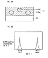
- FIGS. 10 and 11 are schematic cross-sectional views of (SiC)( l-x )(AlN) x crystals grown in Patent Literatures 1 to 3.
- Figures 10 and 11 show that, in a (SiC)( l-x )(AlN) x layer 112 grown by a sublimation method or a MBE method, SiC layers 112a and AIN layers 112b are often layered, as illustrated in Fig.
- SiC layer 112a is often interspersed with aggregated AIN layers 112b, as illustrated in Fig. 11 .
- a mixed crystal state of four elements Si, carbon (C), aluminum (Al), and nitrogen (N) cannot be formed in a (SiC)( l - x) (AlN) x layer 112.
- the present inventor found that the reason that Si (l-v-w-x) C w Al x N v crystals in a mixed crystal state could not be formed is that the sublimation method and the MBE method grow Si (l-v-w-x) C w Al x N v crystals in an equilibrium state.
- the present inventor also found that because SiC and AlN are stable in a Si (l-v-w-x) C w Al x N v layer grown in an equilibrium state, Si bonds to C, and Al bonds to N.
- a method for manufacturing a Si (l-v-w-x) C w Al x N v substrate includes the following steps. First, a Si substrate is prepared. A Si( l-v-w-x )C w Al x N v layer (0 ⁇ v ⁇ 1,0 ⁇ w ⁇ 1,0 ⁇ x ⁇ 1, and 0 ⁇ v+w+x ⁇ 1)is then grown on the Si substrate by a pulsed laser deposition (PLD) method.
- PLD pulsed laser deposition
- a Si (l-v-w-x) C w Al x N v layer (0 ⁇ v ⁇ 1,0 ⁇ w ⁇ 1,0 ⁇ x ⁇ 1, and 0 ⁇ v+w+x ⁇ 1)is grown by a PLD method.
- a raw material for the Si (l-v-w-x) C w Al x N v layer can be irradiated with a laser beam to generate plasma.
- the plasma can be supplied to the surface of the Si substrate.
- the Si (l-v-w-x) C w Al x N v layer can be grown in a non-equilibrium state.
- the Si (l-v-w-x) C w Al x N v layer is grown on the Si substrate.
- Si substrates can be easily cleaved and easily etched with an acid. It is therefore easy to reduce the thickness of a Si substrate or remove a Si substrate.
- an easily processable Si (l-v-w-x) C w Al x N v substrate can be manufactured.
- the method for manufacturing a Si (l-v-w-x) C w Al x N v substrate described above further includes the step of removing the Si substrate after the growing step.
- the Si substrate can be easily processed.
- the Si substrate can therefore be easily removed.
- a Si (l-v-w-x) C w Al x N v substrate that includes no Si substrate and a Si (l-v-w-x) C w Al x N v layer having a reduced number of cracks can be easily manufactured.
- a method for manufacturing an epitaxial wafer according to the present invention includes the steps of manufacturing a Si (l-v-w-x) C w Al x N v substrate by any of the methods for manufacturing a Si (l-v-w-x) C w Al x N v substrate described above and growing an Al (l-y-z )Ga y In z N layer (0 ⁇ y ⁇ 1, 0 ⁇ z ⁇ 1, and 0 ⁇ y + z ⁇ 1) on the Si (l-v-w-x) C w Al x N v layer.
- a Si (l-v-w-x) C w Al x N v layer in a mixed crystal state can be manufactured by a method for manufacturing an epitaxial wafer according to the present invention.
- An Al (l-y-z) GayIn z N layer having uniform crystallinity can therefore be grown on the Si (l-v-w-x) C w Al x N v layer.
- the lattice matching and thermal expansion coefficient of the Al (l-y-z )Gayln z N layer are similar to the lattice matching and thermal expansion coefficient of the Si (l-v-w-x) C w Al x N v layer. This can improve the crystallinity of the Al (l-y-z) Gayln z N layer.
- the Si substrate can be easily removed from the epitaxial wafer.
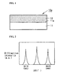
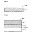
- the Si (l-v-w-x) C w Al x N v substrate 10a includes a Si substrate 11 and a Si (l-v-w-x) C w Al x N v layer 12(0 ⁇ v ⁇ 1,0 ⁇ w ⁇ 1, 0 ⁇ x ⁇ 1, and 0 ⁇ v+w+x ⁇ 1) formed on the main surface 11 a of the Si substrate 11.
- a method for manufacturing a Si (l-v-w-x) C w Al x N v substrate 10a includes the steps of preparing the Si substrate 11 and growing the Si (l-v-w-x) C w Al x N v layer 12(0 ⁇ v ⁇ 1,0 ⁇ w ⁇ 1,0 ⁇ x ⁇ 1,and0 ⁇ v+w+x ⁇ 1) on the Si substrate 11 by a PLD method.
- the Al (l-y-z )Ga y In z N layer 21 is formed on the Si (l-v-w-x) C w Al x N v substrate 10a.
- the Si (l-v-w-x) C w Al x Ny substrate 10a includes the Si (l-v-w-x) C w Al x N v layer 12 in a mixed crystal state.
- An Al (l-y-z) Ga y In z N layer 21 having uniform crystallinity can therefore be grown on the Si (l-v-w-x) C w Al x N v layer 12.
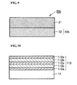
- Figure 9 is a schematic cross-sectional view of an epitaxial wafer according to the present embodiment.
- An epitaxial wafer 20b according to the present embodiment will be described below with reference to Fig. 9 .
- the epitaxial wafer 20b includes the Si (l-v-w-x) C w Al x N v layer 12 and the Al (l-y-z) Ga y In z N layer 21 formed on the Si (l-v-w-x) C w Al x N v layer 12.
- the Si (l-v-w-x) C w Al x N v substrate 10b is manufactured by the method for manufacturing a Si (l-v-w-x) C w Al x N v substrate 10b according to the second embodiment.
- the Al (l-y-z) Ga y In z N layer 21 is then grown on the Si (l-v-w-x) C w Al x N v substrate 10b (the Si (l-v-w-x) C w Al x N v layer 12 in the present embodiment) as in the third embodiment.
- the epitaxial wafer 20b illustrated in Fig. 9 can be manufactured.
- the Al (l-y-z) Ga y In z N layer 21 is formed on the Si (l-v-w-x) C w Al x N v substrate 10b. Since the Si (l-v-w-x )C w Al x N v substrate 10b includes the Si (l-v-w-x) C w Al x N v layer 12 in a mixed crystal state, the Al (l-y-z) Ga y In z N layer 21 having uniform crystallinity can be grown.
- a Si (l-v-w-x) C w Al x N v substrate 10a was basically manufactured by the method for manufacturing a Si (l-v-w-x) C w Al x N v substrate 10a according to the first embodiment with a PLD apparatus illustrated in Fig. 6 .
- Si 0.05 C 0.05 (AlN) 0.9 wherein v+ x was 0.9 was produced as a Si (l-v-w-x) C w Al x N v layer 12.
- the raw material 103 for a Si 0.05 C 0.05 (AlN) 0.9 layer 12 was first prepared.
- the raw material 103 was prepared in the following way. More specifically, a SiC powder and an AIN powder were mixed and pressed. This mixture was placed in a vacuum vessel. After the vacuum vessel was evacuated to 10 -6 Torr, the atmosphere was filled with a high-purity Ar gas, The mixture was then fired at 2300°C for 20 hours to prepare the raw material 103. The raw material 103 was placed on the stage 104 illustrated in Fig. 6 .
- a Si substrate 11 was then prepared as a base substrate.
- the Si substrate 11 had a (001) plane as a main surface 11a and a size of one inch.
- the Si substrate 11 was placed on the surface of a substrate holder 106 in a vacuum chamber 101 such that the Si substrate 11 faced the raw material 103.
- the vacuum chamber 101 was evacuated to 1 x 10 -6 Torr and was then filled with nitrogen.
- the Si 0.05 C 0.05 (AlN) 0.9 layer 12 having a thickness of 500 nm was grown while monitoring the thickness through the oscillation of a RHEED 108 installed on the vacuum chamber 101.
- a Si 0.05 C 0.05 (AlN) 0.9 substrate was manufactured basically in the same manner as in Working Example 1 except that the Si substrate serving as a base substrate was replaced with a sapphire substrate having a (0001) main surface.
- a Si 0.05 C 0.05 (AlN) 0.9 substrate was manufactured basically in the same manner as in Working Example 1 except that the Si substrate serving as a base substrate was replaced with a 6H-SiC substrate having a (0001) main surface.
- Table I shows the results. In Table I, “Pass” means that the base substrate was successfully removed, and “Fail” means that the base substrate was not successfully removed.
- Table I shows that the Si 0.05 C 0.05 (AlN) 0.9 substrate according to Working Example 1, which used the Si substrate as the base substrate, exhibited excellent etching characteristics and cleavability of the Si substrate. This showed that the Si substrate could be easily processed.
- the Si 0.05 C 0.05 (AlN) 0.9 substrate according to Comparative Example 2 which used the SiC substrate as the base substrate, exhibited poor etching characteristics of the SiC substrate. The SiC substrate was therefore not sufficiently removed by etching.
- the present example showed that a Si (l-v-w-x) C w Al x N v substrate that can be easily processed can be manufactured using a Si substrate.
- Si 0.05 C 0.05 (AlN) 0.45 was grown basically in the same manner as in Working Example 1 except that a Si substrate 11 having a (111) main surface was used as the base substrate.
- Working Example 3 was basically the same as Working Example 2 except that the Si (l-v-w-x) C w Al x N v layer 12 grown was Si 0.0005 C 0.0005 Al 0.4994 N 0.4996 . This change was achieved by altering the molar ratio of the AIN powder to the SiC powder in the raw material 103 prepared.
- Working Example 4 was basically the same as Working Example 2 except that the Si (l-v-w-x) C w Al x N v layer 12 grown was Si 0.0005 C 0.0005 Al 0 , 4996 N 0 . 4994 .
- Working Example 6 was basically the same as Working Example 2 except that the Si (l-v-w-x) C w Al x N v layer 12 grown was Si 0.0006 C 0.0004 Al 0 . 4995 N 0.4995 .
- Working Example 7 was basically the same as Working Example 2 except that the Si (l-v-w-x) C w Al x N v layer 12 grown was Si 0.0004 C 0.0006 Al 0.4995 N 0.4995 .
- Working Example 8 was basically the same as Working Example 2 except that the Si (l-v-w-x) C w Al x N v layer 12 grown was Si 0.005 C 0.005 Al 0.495 N 0.495 .
- Working Example 9 was basically the same as Working Example 1 except that the Si (l-v-w-x) C w Al x N v layer 12 grown was Si 0.25 C 0.25 Al 0.25 N 0.25 .
- Working Example 10 was basically the same as Working Example 1 except that the Si (l-v-w-x) C w Al x N v layer 12 grown was Si 0.45 C 0.45 Al 0.05 N 0.05 .
- Working Example 11 was basically the same as Working Example 2 except that the Si (l-v-w-x) C w Al x N v layer 12 grown was Si 0.495 C 0.495 Al 0.005 N 0.005 .
- Working Example 12 was basically the same as Working Example 2 except that the Si (l-v-w-x) C w Al x N v layer 12 grown was Si 0 , 4995 C 0.4995 Al 0.0004 N 0.0006 .
- Working Example 13 was basically the same as Working Example 2 except that the Si (l-v-w-x) C w Al x N v layer 12 grown was Si 0 . 499S C 0.4995 Al 0 . 0006 N 0.0004 ⁇
- Working Example 14 was basically the same as Working Example 2 except that the Si (l-v-w-x) C w Al x N v layer 12 grown was Si 0.4995 C 0.4995 Al 0.0005 N 0.0005 .
- Working Example 15 was basically the same as Working Example 2 except that the Si (l-v-w-x) C w Al x N v layer 12 grown was Si 0.4996 C 0.4994 Al 0.0005 N 0.0005 .
- Working Example 17 was basically the same as Working Example 2 except that the Si 0.05 C 0.05 Al 0 . 45 N 0.45 layer was grown at a temperature of the main surface of the Si substrate of 550°C.
- Working Example 18 was basically the same as Working Example 2 except that a Si 0.0005 C 0.0005 Al 0.4994 N 0.4996 layer was grown at a temperature of the main surface of the Si substrate of 550°C.
- Working Example 19 was basically the same as Working Example 2 except that a Si 0.0005 C 0.0005 Al 0.4996 N 0.4994 layer was grown at a temperature of the main surface of the Si substrate of 550°C.
- Working Example 20 was basically the same as Working Example 2 except that a Si 0.0005 C 0.0005 Al 0 , 4995 N 0.4995 layer was grown at a temperature of the main surface of the Si substrate of 550°C.
- Working Example 21 was basically the same as Working Example 2 except that a Si 0.0006 C 0.0004 Al 0.4995 N 0.4995 layer was grown at a temperature of the main surface of the Si substrate of 550°C.
- Working Example 22 was basically the same as Working Example 2 except that a Si 0.0004 C 0.0006 Al 0 . 4995 N 0.4995 layer was grown at a temperature of the main surface of the Si substrate of 550°C.
- Working Example 23 was basically the same as Working Example 2 except that a Si 0.005 C 0.005 Al 0.495 N 0.495 layer was grown at a temperature of the main surface of the Si substrate of 550°C.
- Working Example 25 was basically the same as Working Example 2 except that a Si 0.45 C 0.45 Al 0.05 N 0.05 layer was grown at a temperature of the main surface of the Si substrate of 550°C.
- Working Example 26 was basically the same as Working Example 2 except that a Si 0.495 C 0.495 Al 0.005 N 0.005 layer was grown at a temperature of the main surface of the Si substrate of 550°C.
- Working Example 27 was basically the same as Working Example 2 except that a Si 0.4995 C 0.4995 Al 0.0004 N 0.0006 layer was grown at a temperature of the main surface of the Si substrate of 550°C.
- Working Example 28 was basically the same as Working Example 2 except that a Si 0.4995 C 0.4995 Al 0.0006 N 0.0004 layer was grown at a temperature of the main surface of the Si substrate of 550°C.
- Working Example 29 was basically the same as Working Example 2 except that a Si 0.4995 C 0.4995 Al 0 . 0005 N 0.0005 layer was grown at a temperature of the main surface of the Si substrate of 550°C.
- Comparative Example 6 was basically the same as Working Example 2 except that a SiC layer was grown at a temperature of the main surface of the Si substrate of 550°C.
- the number of cracks in the Si 0.25 C 0.25 Al 0.25 N 0.25 layer grown at 540°C in Working Example 9 was five.
- the number of cracks in the Si 0.25 C 0.25 Al 0.25 N 0.25 layer, which had the same composition as in Working Example 5, grown at 550°C in Comparative Example 24 was six.
- the number of cracks in the Si (l-v-w-x) C w Al x N v layer in which v + x was 0.1, 0.01, or 0.001 grown at 540°C in Working Examples 10 to 16 was three.
- the number of cracks in the Si (l-v-w-x) C w Al x N v layer in which v + x was 0.1, 0.01, or 0.001 grown at 550°C in Comparative Examples 25 to 31 was four.
- a Si (l-v-w-x) C w Al x N v layer having a larger v + x has a larger difference in composition from the Si substrate 11, resulting in an increased number of cracks.
- Table II shows that the numbers of cracks in a Si (l-v-w-x) C w Al x N v layer grown at 540°C were seven or less for 1 > v + x > 0.5, five or less for 0.5 ⁇ v + x > 0.1, and three or less for 0.1 ⁇ v + x >0.
- the present example showed that a Si (l-v-w-x) C w Al x N v layer (0 ⁇ v + x ⁇ 1) grown at a temperature below 550°C can reduce the number of cracks in the Si (l-v-w-x) C w Al x N v layer (0 ⁇ v + x ⁇ 1).
Landscapes
- Chemical & Material Sciences (AREA)
- Engineering & Computer Science (AREA)
- Materials Engineering (AREA)
- Metallurgy (AREA)
- Organic Chemistry (AREA)
- Crystallography & Structural Chemistry (AREA)
- Inorganic Chemistry (AREA)
- Chemical Kinetics & Catalysis (AREA)
- Mechanical Engineering (AREA)
- Health & Medical Sciences (AREA)
- Toxicology (AREA)
- Crystals, And After-Treatments Of Crystals (AREA)
- Recrystallisation Techniques (AREA)
- Physical Vapour Deposition (AREA)
Applications Claiming Priority (3)
| Application Number | Priority Date | Filing Date | Title |
|---|---|---|---|
| JP2008114467 | 2008-04-24 | ||
| JP2009056915A JP2009280903A (ja) | 2008-04-24 | 2009-03-10 | Si(1−v−w−x)CwAlxNv基材の製造方法、エピタキシャルウエハの製造方法、Si(1−v−w−x)CwAlxNv基材およびエピタキシャルウエハ |
| PCT/JP2009/057723 WO2009131064A1 (fr) | 2008-04-24 | 2009-04-17 | Procede de production de materiau de base si<sb>(1-v-w-x)</sb>c<sb>w</sb>al<sb>x</sb>n<sb>v</sb>, procede de production de tranche epitaxiale, materiau de base si<sb>(1-v-w-x)</sb>c<sb>w</sb>al<sb>x</sb>n<sb>v</sb> et tranche epitaxiale ainsi produits |
Publications (3)
| Publication Number | Publication Date |
|---|---|
| EP2276060A1 true EP2276060A1 (fr) | 2011-01-19 |
| EP2276060A4 EP2276060A4 (fr) | 2013-10-16 |
| EP2276060B1 EP2276060B1 (fr) | 2015-02-25 |
Family
ID=41216800
Family Applications (1)
| Application Number | Title | Priority Date | Filing Date |
|---|---|---|---|
| EP09733673.9A Not-in-force EP2276060B1 (fr) | 2008-04-24 | 2009-04-17 | Procede de production de materiau de base si(1-v-w-x)cwalxnv et procede de production de tranche epitaxiale |
Country Status (6)
| Country | Link |
|---|---|
| US (2) | US8357597B2 (fr) |
| EP (1) | EP2276060B1 (fr) |
| JP (1) | JP2009280903A (fr) |
| KR (1) | KR20100137534A (fr) |
| CN (1) | CN102017080B (fr) |
| WO (1) | WO2009131064A1 (fr) |
Cited By (1)
| Publication number | Priority date | Publication date | Assignee | Title |
|---|---|---|---|---|
| EP4312248A1 (fr) * | 2022-07-27 | 2024-01-31 | Siltronic AG | Tranche hétéroépitaxiale pour le dépôt de nitrure de gallium |
Families Citing this family (3)
| Publication number | Priority date | Publication date | Assignee | Title |
|---|---|---|---|---|
| JP5621199B2 (ja) * | 2008-04-24 | 2014-11-05 | 住友電気工業株式会社 | Si(1−v−w−x)CwAlxNv基材の製造方法、エピタキシャルウエハの製造方法、Si(1−v−w−x)CwAlxNv基材およびエピタキシャルウエハ |
| JP2009280484A (ja) * | 2008-04-24 | 2009-12-03 | Sumitomo Electric Ind Ltd | Si(1−v−w−x)CwAlxNv基材の製造方法、エピタキシャルウエハの製造方法、Si(1−v−w−x)CwAlxNv基材およびエピタキシャルウエハ |
| KR101346415B1 (ko) * | 2008-08-29 | 2014-01-02 | 미쓰비시덴키 가부시키가이샤 | SiC 단결정막의 제조 방법 및 장치 |
Family Cites Families (17)
| Publication number | Priority date | Publication date | Assignee | Title |
|---|---|---|---|---|
| US4382837A (en) | 1981-06-30 | 1983-05-10 | International Business Machines Corporation | Epitaxial crystal fabrication of SiC:AlN |
| JPS61291495A (ja) * | 1985-06-18 | 1986-12-22 | Sharp Corp | 炭化珪素単結晶基板の製造方法 |
| JPH067594B2 (ja) | 1987-11-20 | 1994-01-26 | 富士通株式会社 | 半導体基板の製造方法 |
| JPH04167477A (ja) | 1990-10-31 | 1992-06-15 | Toshiba Corp | 半導体素子 |
| US6086672A (en) | 1998-10-09 | 2000-07-11 | Cree, Inc. | Growth of bulk single crystals of aluminum nitride: silicon carbide alloys |
| US6911084B2 (en) * | 2001-09-26 | 2005-06-28 | Arizona Board Of Regents | Low temperature epitaxial growth of quaternary wide bandgap semiconductors |
| KR20040058206A (ko) * | 2001-10-16 | 2004-07-03 | 아리조나 보드 오브 리전트스, 아리조나주의 아리조나 주립대 대행법인 | 4원 광 밴드갭 반도체의 저온 에피택셜 성장 |
| WO2004073045A2 (fr) | 2003-02-12 | 2004-08-26 | Arizona Board Of Regents, A Body Corporate Of The State Of Arizona, Acting For And On Behalf Of Arizona State University | Croissance epitaxiale de nitrures du groupe iii sur des substrats en silicium par l'intermediaire d'une couche reflechissante tampon de diborure de zirconium presentant une correspondance de reseau moleculaire avec un substrat |
| US7250648B2 (en) | 2003-09-04 | 2007-07-31 | Intematix Corporation | Ferroelectric rare-earth manganese-titanium oxides |
| KR100659579B1 (ko) * | 2004-12-08 | 2006-12-20 | 한국전자통신연구원 | 발광 소자 및 발광 소자의 제조방법 |
| WO2007049939A1 (fr) | 2005-10-29 | 2007-05-03 | Samsung Electronics Co., Ltd. | Dispositif semi-conducteur et procede de fabrication |
| US7371282B2 (en) | 2006-07-12 | 2008-05-13 | Northrop Grumman Corporation | Solid solution wide bandgap semiconductor materials |
| CN100588737C (zh) * | 2007-03-30 | 2010-02-10 | 中国科学院上海硅酸盐研究所 | 一种p型含铜硫透明导体薄膜的制备方法 |
| US20080277778A1 (en) * | 2007-05-10 | 2008-11-13 | Furman Bruce K | Layer Transfer Process and Functionally Enhanced Integrated Circuits Products Thereby |
| JP5621199B2 (ja) * | 2008-04-24 | 2014-11-05 | 住友電気工業株式会社 | Si(1−v−w−x)CwAlxNv基材の製造方法、エピタキシャルウエハの製造方法、Si(1−v−w−x)CwAlxNv基材およびエピタキシャルウエハ |
| JP2009280484A (ja) * | 2008-04-24 | 2009-12-03 | Sumitomo Electric Ind Ltd | Si(1−v−w−x)CwAlxNv基材の製造方法、エピタキシャルウエハの製造方法、Si(1−v−w−x)CwAlxNv基材およびエピタキシャルウエハ |
| US8247249B2 (en) | 2010-06-01 | 2012-08-21 | Palo Alto Research Center Incorporated | Semi-polar nitride-based light emitting structure and method of forming same |
-
2009
- 2009-03-10 JP JP2009056915A patent/JP2009280903A/ja active Pending
- 2009-04-17 US US12/989,039 patent/US8357597B2/en not_active Expired - Fee Related
- 2009-04-17 EP EP09733673.9A patent/EP2276060B1/fr not_active Not-in-force
- 2009-04-17 WO PCT/JP2009/057723 patent/WO2009131064A1/fr not_active Ceased
- 2009-04-17 CN CN200980114395.5A patent/CN102017080B/zh not_active Expired - Fee Related
- 2009-04-17 KR KR1020107023484A patent/KR20100137534A/ko not_active Abandoned
-
2012
- 2012-12-14 US US13/715,254 patent/US8937339B2/en not_active Expired - Fee Related
Cited By (2)
| Publication number | Priority date | Publication date | Assignee | Title |
|---|---|---|---|---|
| EP4312248A1 (fr) * | 2022-07-27 | 2024-01-31 | Siltronic AG | Tranche hétéroépitaxiale pour le dépôt de nitrure de gallium |
| WO2024023004A1 (fr) * | 2022-07-27 | 2024-02-01 | Siltronic Ag | Tranche hétéroépitaxiale pour le dèpôt de nitrure de gallium |
Also Published As
| Publication number | Publication date |
|---|---|
| JP2009280903A (ja) | 2009-12-03 |
| CN102017080A (zh) | 2011-04-13 |
| US20130105858A1 (en) | 2013-05-02 |
| EP2276060B1 (fr) | 2015-02-25 |
| US8357597B2 (en) | 2013-01-22 |
| CN102017080B (zh) | 2013-04-24 |
| EP2276060A4 (fr) | 2013-10-16 |
| WO2009131064A1 (fr) | 2009-10-29 |
| US8937339B2 (en) | 2015-01-20 |
| US20110042788A1 (en) | 2011-02-24 |
| KR20100137534A (ko) | 2010-12-30 |
Similar Documents
| Publication | Publication Date | Title |
|---|---|---|
| US12351941B2 (en) | Ground substrate and method for producing same | |
| EP2471981A1 (fr) | Tranche de monocristal de sic et son procédé de fabrication | |
| EP1832673B1 (fr) | Procédé pour la production d'un substrat pour la croissance de diamant monocristallin | |
| KR20120001606A (ko) | 단결정 다이아몬드 성장용 기재 및 단결정 다이아몬드 기판의 제조 방법 | |
| US8715414B2 (en) | Process for producing Si(1-v-w-x)CwAlxNv base material, process for producing epitaxial wafer, Si(1-v-w-x)CwAlxNv base material, and epitaxial wafer | |
| US20250154681A1 (en) | Aluminum nitride single crystals having large crystal augmentation parameters | |
| EP2264228A1 (fr) | Monocristal massif d'aln, dispositif semi-conducteur et procédé de production de monocristal massif d'aln | |
| US8937339B2 (en) | Si(1-V-W-X)CWAlXNV substrate, and epitaxial wafer | |
| EP2302110B1 (fr) | Procédé de fabrication d'un substrat de si(1-v-w-x)cwalxnv, procédé de fabrication d'une tranche épitaxiale, substrat de si(1-v-w-x)cwalxnv et tranche épitaxiale | |
| US12571127B2 (en) | Ultra-high thermal-conductivity diamond and synthetic method therefor | |
| Bensaoula et al. | The nitridation of GaAs and GaN deposition on GaAs examined by in situ time-of-flight low energy ion scattering and RHEED | |
| US20260068551A1 (en) | Underlying substrate, single crystal diamond laminate substrate and method for producing them | |
| TW202543958A (zh) | 複合基板及裝置 | |
| WO2024224665A1 (fr) | SUBSTRAT DE SiC ET SUBSTRAT COMPOSITE DE SiC | |
| WO2025203255A1 (fr) | Substrat composite, élément semi-conducteur et procédé de fabrication de substrat composite | |
| JP2003026500A (ja) | 結晶性SiC薄膜の構造およびその製造方法 | |
| Baerwolff et al. | Calculation of the yield of fault-free laser diodes from the characteristics of the (100) InP substrate material used in epitaxial double heterostructures | |
| WO2000061839A1 (fr) | Nitrure d'aluminium cubique (a base de sphalerite) et procede de production dudit nitrure | |
| KR20130025629A (ko) | 박막 성장방법 |
Legal Events
| Date | Code | Title | Description |
|---|---|---|---|
| PUAI | Public reference made under article 153(3) epc to a published international application that has entered the european phase |
Free format text: ORIGINAL CODE: 0009012 |
|
| 17P | Request for examination filed |
Effective date: 20101020 |
|
| AK | Designated contracting states |
Kind code of ref document: A1 Designated state(s): AT BE BG CH CY CZ DE DK EE ES FI FR GB GR HR HU IE IS IT LI LT LU LV MC MK MT NL NO PL PT RO SE SI SK TR |
|
| AX | Request for extension of the european patent |
Extension state: AL BA RS |
|
| DAX | Request for extension of the european patent (deleted) | ||
| REG | Reference to a national code |
Ref country code: DE Ref legal event code: R079 Ref document number: 602009029545 Country of ref document: DE Free format text: PREVIOUS MAIN CLASS: H01L0021205000 Ipc: C30B0029380000 |
|
| A4 | Supplementary search report drawn up and despatched |
Effective date: 20130912 |
|
| RIC1 | Information provided on ipc code assigned before grant |
Ipc: C30B 29/36 20060101ALI20130906BHEP Ipc: C30B 29/40 20060101ALI20130906BHEP Ipc: C30B 23/08 20060101ALI20130906BHEP Ipc: C30B 25/02 20060101ALI20130906BHEP Ipc: H01L 29/267 20060101ALI20130906BHEP Ipc: C23C 14/28 20060101ALI20130906BHEP Ipc: C30B 29/38 20060101AFI20130906BHEP Ipc: C30B 23/02 20060101ALI20130906BHEP Ipc: C23C 14/06 20060101ALI20130906BHEP Ipc: H01L 21/02 20060101ALI20130906BHEP |
|
| 17Q | First examination report despatched |
Effective date: 20140502 |
|
| GRAP | Despatch of communication of intention to grant a patent |
Free format text: ORIGINAL CODE: EPIDOSNIGR1 |
|
| INTG | Intention to grant announced |
Effective date: 20140919 |
|
| GRAS | Grant fee paid |
Free format text: ORIGINAL CODE: EPIDOSNIGR3 |
|
| GRAA | (expected) grant |
Free format text: ORIGINAL CODE: 0009210 |
|
| AK | Designated contracting states |
Kind code of ref document: B1 Designated state(s): AT BE BG CH CY CZ DE DK EE ES FI FR GB GR HR HU IE IS IT LI LT LU LV MC MK MT NL NO PL PT RO SE SI SK TR |
|
| REG | Reference to a national code |
Ref country code: GB Ref legal event code: FG4D |
|
| REG | Reference to a national code |
Ref country code: CH Ref legal event code: EP |
|
| REG | Reference to a national code |
Ref country code: IE Ref legal event code: FG4D |
|
| REG | Reference to a national code |
Ref country code: DE Ref legal event code: R096 Ref document number: 602009029545 Country of ref document: DE Effective date: 20150402 |
|
| REG | Reference to a national code |
Ref country code: AT Ref legal event code: REF Ref document number: 712093 Country of ref document: AT Kind code of ref document: T Effective date: 20150415 |
|
| REG | Reference to a national code |
Ref country code: NL Ref legal event code: VDEP Effective date: 20150225 |
|
| REG | Reference to a national code |
Ref country code: AT Ref legal event code: MK05 Ref document number: 712093 Country of ref document: AT Kind code of ref document: T Effective date: 20150225 |
|
| REG | Reference to a national code |
Ref country code: LT Ref legal event code: MG4D |
|
| PG25 | Lapsed in a contracting state [announced via postgrant information from national office to epo] |
Ref country code: ES Free format text: LAPSE BECAUSE OF FAILURE TO SUBMIT A TRANSLATION OF THE DESCRIPTION OR TO PAY THE FEE WITHIN THE PRESCRIBED TIME-LIMIT Effective date: 20150225 Ref country code: SE Free format text: LAPSE BECAUSE OF FAILURE TO SUBMIT A TRANSLATION OF THE DESCRIPTION OR TO PAY THE FEE WITHIN THE PRESCRIBED TIME-LIMIT Effective date: 20150225 Ref country code: FI Free format text: LAPSE BECAUSE OF FAILURE TO SUBMIT A TRANSLATION OF THE DESCRIPTION OR TO PAY THE FEE WITHIN THE PRESCRIBED TIME-LIMIT Effective date: 20150225 Ref country code: HR Free format text: LAPSE BECAUSE OF FAILURE TO SUBMIT A TRANSLATION OF THE DESCRIPTION OR TO PAY THE FEE WITHIN THE PRESCRIBED TIME-LIMIT Effective date: 20150225 Ref country code: NO Free format text: LAPSE BECAUSE OF FAILURE TO SUBMIT A TRANSLATION OF THE DESCRIPTION OR TO PAY THE FEE WITHIN THE PRESCRIBED TIME-LIMIT Effective date: 20150525 Ref country code: LT Free format text: LAPSE BECAUSE OF FAILURE TO SUBMIT A TRANSLATION OF THE DESCRIPTION OR TO PAY THE FEE WITHIN THE PRESCRIBED TIME-LIMIT Effective date: 20150225 |
|
| PG25 | Lapsed in a contracting state [announced via postgrant information from national office to epo] |
Ref country code: AT Free format text: LAPSE BECAUSE OF FAILURE TO SUBMIT A TRANSLATION OF THE DESCRIPTION OR TO PAY THE FEE WITHIN THE PRESCRIBED TIME-LIMIT Effective date: 20150225 Ref country code: IS Free format text: LAPSE BECAUSE OF FAILURE TO SUBMIT A TRANSLATION OF THE DESCRIPTION OR TO PAY THE FEE WITHIN THE PRESCRIBED TIME-LIMIT Effective date: 20150625 Ref country code: GR Free format text: LAPSE BECAUSE OF FAILURE TO SUBMIT A TRANSLATION OF THE DESCRIPTION OR TO PAY THE FEE WITHIN THE PRESCRIBED TIME-LIMIT Effective date: 20150526 Ref country code: LV Free format text: LAPSE BECAUSE OF FAILURE TO SUBMIT A TRANSLATION OF THE DESCRIPTION OR TO PAY THE FEE WITHIN THE PRESCRIBED TIME-LIMIT Effective date: 20150225 |
|
| PG25 | Lapsed in a contracting state [announced via postgrant information from national office to epo] |
Ref country code: NL Free format text: LAPSE BECAUSE OF FAILURE TO SUBMIT A TRANSLATION OF THE DESCRIPTION OR TO PAY THE FEE WITHIN THE PRESCRIBED TIME-LIMIT Effective date: 20150225 |
|
| PG25 | Lapsed in a contracting state [announced via postgrant information from national office to epo] |
Ref country code: EE Free format text: LAPSE BECAUSE OF FAILURE TO SUBMIT A TRANSLATION OF THE DESCRIPTION OR TO PAY THE FEE WITHIN THE PRESCRIBED TIME-LIMIT Effective date: 20150225 Ref country code: DK Free format text: LAPSE BECAUSE OF FAILURE TO SUBMIT A TRANSLATION OF THE DESCRIPTION OR TO PAY THE FEE WITHIN THE PRESCRIBED TIME-LIMIT Effective date: 20150225 Ref country code: RO Free format text: LAPSE BECAUSE OF FAILURE TO SUBMIT A TRANSLATION OF THE DESCRIPTION OR TO PAY THE FEE WITHIN THE PRESCRIBED TIME-LIMIT Effective date: 20150225 Ref country code: SK Free format text: LAPSE BECAUSE OF FAILURE TO SUBMIT A TRANSLATION OF THE DESCRIPTION OR TO PAY THE FEE WITHIN THE PRESCRIBED TIME-LIMIT Effective date: 20150225 Ref country code: CZ Free format text: LAPSE BECAUSE OF FAILURE TO SUBMIT A TRANSLATION OF THE DESCRIPTION OR TO PAY THE FEE WITHIN THE PRESCRIBED TIME-LIMIT Effective date: 20150225 |
|
| REG | Reference to a national code |
Ref country code: DE Ref legal event code: R097 Ref document number: 602009029545 Country of ref document: DE |
|
| PG25 | Lapsed in a contracting state [announced via postgrant information from national office to epo] |
Ref country code: LU Free format text: LAPSE BECAUSE OF FAILURE TO SUBMIT A TRANSLATION OF THE DESCRIPTION OR TO PAY THE FEE WITHIN THE PRESCRIBED TIME-LIMIT Effective date: 20150417 Ref country code: PL Free format text: LAPSE BECAUSE OF FAILURE TO SUBMIT A TRANSLATION OF THE DESCRIPTION OR TO PAY THE FEE WITHIN THE PRESCRIBED TIME-LIMIT Effective date: 20150225 Ref country code: MC Free format text: LAPSE BECAUSE OF FAILURE TO SUBMIT A TRANSLATION OF THE DESCRIPTION OR TO PAY THE FEE WITHIN THE PRESCRIBED TIME-LIMIT Effective date: 20150225 |
|
| REG | Reference to a national code |
Ref country code: CH Ref legal event code: PL |
|
| PG25 | Lapsed in a contracting state [announced via postgrant information from national office to epo] |
Ref country code: IT Free format text: LAPSE BECAUSE OF FAILURE TO SUBMIT A TRANSLATION OF THE DESCRIPTION OR TO PAY THE FEE WITHIN THE PRESCRIBED TIME-LIMIT Effective date: 20150225 |
|
| PLBE | No opposition filed within time limit |
Free format text: ORIGINAL CODE: 0009261 |
|
| STAA | Information on the status of an ep patent application or granted ep patent |
Free format text: STATUS: NO OPPOSITION FILED WITHIN TIME LIMIT |
|
| GBPC | Gb: european patent ceased through non-payment of renewal fee |
Effective date: 20150525 |
|
| REG | Reference to a national code |
Ref country code: IE Ref legal event code: MM4A |
|
| PG25 | Lapsed in a contracting state [announced via postgrant information from national office to epo] |
Ref country code: LI Free format text: LAPSE BECAUSE OF NON-PAYMENT OF DUE FEES Effective date: 20150430 Ref country code: CH Free format text: LAPSE BECAUSE OF NON-PAYMENT OF DUE FEES Effective date: 20150430 |
|
| 26N | No opposition filed |
Effective date: 20151126 |
|
| PG25 | Lapsed in a contracting state [announced via postgrant information from national office to epo] |
Ref country code: SI Free format text: LAPSE BECAUSE OF FAILURE TO SUBMIT A TRANSLATION OF THE DESCRIPTION OR TO PAY THE FEE WITHIN THE PRESCRIBED TIME-LIMIT Effective date: 20150225 |
|
| REG | Reference to a national code |
Ref country code: FR Ref legal event code: PLFP Year of fee payment: 8 |
|
| PG25 | Lapsed in a contracting state [announced via postgrant information from national office to epo] |
Ref country code: GB Free format text: LAPSE BECAUSE OF NON-PAYMENT OF DUE FEES Effective date: 20150525 Ref country code: IE Free format text: LAPSE BECAUSE OF NON-PAYMENT OF DUE FEES Effective date: 20150417 |
|
| PG25 | Lapsed in a contracting state [announced via postgrant information from national office to epo] |
Ref country code: BE Free format text: LAPSE BECAUSE OF FAILURE TO SUBMIT A TRANSLATION OF THE DESCRIPTION OR TO PAY THE FEE WITHIN THE PRESCRIBED TIME-LIMIT Effective date: 20150225 |
|
| PG25 | Lapsed in a contracting state [announced via postgrant information from national office to epo] |
Ref country code: MT Free format text: LAPSE BECAUSE OF FAILURE TO SUBMIT A TRANSLATION OF THE DESCRIPTION OR TO PAY THE FEE WITHIN THE PRESCRIBED TIME-LIMIT Effective date: 20150225 |
|
| REG | Reference to a national code |
Ref country code: FR Ref legal event code: PLFP Year of fee payment: 9 |
|
| PGFP | Annual fee paid to national office [announced via postgrant information from national office to epo] |
Ref country code: FR Payment date: 20170313 Year of fee payment: 9 |
|
| PG25 | Lapsed in a contracting state [announced via postgrant information from national office to epo] |
Ref country code: BG Free format text: LAPSE BECAUSE OF FAILURE TO SUBMIT A TRANSLATION OF THE DESCRIPTION OR TO PAY THE FEE WITHIN THE PRESCRIBED TIME-LIMIT Effective date: 20150225 Ref country code: HU Free format text: LAPSE BECAUSE OF FAILURE TO SUBMIT A TRANSLATION OF THE DESCRIPTION OR TO PAY THE FEE WITHIN THE PRESCRIBED TIME-LIMIT; INVALID AB INITIO Effective date: 20090417 |
|
| PG25 | Lapsed in a contracting state [announced via postgrant information from national office to epo] |
Ref country code: CY Free format text: LAPSE BECAUSE OF FAILURE TO SUBMIT A TRANSLATION OF THE DESCRIPTION OR TO PAY THE FEE WITHIN THE PRESCRIBED TIME-LIMIT Effective date: 20150225 |
|
| PG25 | Lapsed in a contracting state [announced via postgrant information from national office to epo] |
Ref country code: PT Free format text: LAPSE BECAUSE OF FAILURE TO SUBMIT A TRANSLATION OF THE DESCRIPTION OR TO PAY THE FEE WITHIN THE PRESCRIBED TIME-LIMIT Effective date: 20150625 |
|
| PG25 | Lapsed in a contracting state [announced via postgrant information from national office to epo] |
Ref country code: TR Free format text: LAPSE BECAUSE OF FAILURE TO SUBMIT A TRANSLATION OF THE DESCRIPTION OR TO PAY THE FEE WITHIN THE PRESCRIBED TIME-LIMIT Effective date: 20150225 |
|
| PG25 | Lapsed in a contracting state [announced via postgrant information from national office to epo] |
Ref country code: MK Free format text: LAPSE BECAUSE OF FAILURE TO SUBMIT A TRANSLATION OF THE DESCRIPTION OR TO PAY THE FEE WITHIN THE PRESCRIBED TIME-LIMIT Effective date: 20150225 |
|
| PG25 | Lapsed in a contracting state [announced via postgrant information from national office to epo] |
Ref country code: FR Free format text: LAPSE BECAUSE OF NON-PAYMENT OF DUE FEES Effective date: 20180430 |
|
| P01 | Opt-out of the competence of the unified patent court (upc) registered |
Effective date: 20230515 |
|
| PGFP | Annual fee paid to national office [announced via postgrant information from national office to epo] |
Ref country code: DE Payment date: 20240227 Year of fee payment: 16 |
|
| REG | Reference to a national code |
Ref country code: DE Ref legal event code: R119 Ref document number: 602009029545 Country of ref document: DE |
|
| PG25 | Lapsed in a contracting state [announced via postgrant information from national office to epo] |
Ref country code: DE Free format text: LAPSE BECAUSE OF NON-PAYMENT OF DUE FEES Effective date: 20251104 |