EP2276060B1 - Verfahren zur herstellung eines si(1-v-w-x)cwalxnv-basismaterials und verfahren zur herstellung eines epitaxialwafers - Google Patents
Verfahren zur herstellung eines si(1-v-w-x)cwalxnv-basismaterials und verfahren zur herstellung eines epitaxialwafers Download PDFInfo
- Publication number
- EP2276060B1 EP2276060B1 EP09733673.9A EP09733673A EP2276060B1 EP 2276060 B1 EP2276060 B1 EP 2276060B1 EP 09733673 A EP09733673 A EP 09733673A EP 2276060 B1 EP2276060 B1 EP 2276060B1
- Authority
- EP
- European Patent Office
- Prior art keywords
- layer
- substrate
- base substrate
- working example
- grown
- Prior art date
- Legal status (The legal status is an assumption and is not a legal conclusion. Google has not performed a legal analysis and makes no representation as to the accuracy of the status listed.)
- Not-in-force
Links
Images



Classifications
-
- C—CHEMISTRY; METALLURGY
- C30—CRYSTAL GROWTH
- C30B—SINGLE-CRYSTAL GROWTH; UNIDIRECTIONAL SOLIDIFICATION OF EUTECTIC MATERIAL OR UNIDIRECTIONAL DEMIXING OF EUTECTOID MATERIAL; REFINING BY ZONE-MELTING OF MATERIAL; PRODUCTION OF A HOMOGENEOUS POLYCRYSTALLINE MATERIAL WITH DEFINED STRUCTURE; SINGLE CRYSTALS OR HOMOGENEOUS POLYCRYSTALLINE MATERIAL WITH DEFINED STRUCTURE; AFTER-TREATMENT OF SINGLE CRYSTALS OR A HOMOGENEOUS POLYCRYSTALLINE MATERIAL WITH DEFINED STRUCTURE; APPARATUS THEREFOR
- C30B23/00—Single-crystal growth by condensing evaporated or sublimed materials
- C30B23/02—Epitaxial-layer growth
-
- H—ELECTRICITY
- H10—SEMICONDUCTOR DEVICES; ELECTRIC SOLID-STATE DEVICES NOT OTHERWISE PROVIDED FOR
- H10D—INORGANIC ELECTRIC SEMICONDUCTOR DEVICES
- H10D62/00—Semiconductor bodies, or regions thereof, of devices having potential barriers
- H10D62/80—Semiconductor bodies, or regions thereof, of devices having potential barriers characterised by the materials
- H10D62/82—Heterojunctions
-
- C—CHEMISTRY; METALLURGY
- C23—COATING METALLIC MATERIAL; COATING MATERIAL WITH METALLIC MATERIAL; CHEMICAL SURFACE TREATMENT; DIFFUSION TREATMENT OF METALLIC MATERIAL; COATING BY VACUUM EVAPORATION, BY SPUTTERING, BY ION IMPLANTATION OR BY CHEMICAL VAPOUR DEPOSITION, IN GENERAL; INHIBITING CORROSION OF METALLIC MATERIAL OR INCRUSTATION IN GENERAL
- C23C—COATING METALLIC MATERIAL; COATING MATERIAL WITH METALLIC MATERIAL; SURFACE TREATMENT OF METALLIC MATERIAL BY DIFFUSION INTO THE SURFACE, BY CHEMICAL CONVERSION OR SUBSTITUTION; COATING BY VACUUM EVAPORATION, BY SPUTTERING, BY ION IMPLANTATION OR BY CHEMICAL VAPOUR DEPOSITION, IN GENERAL
- C23C14/00—Coating by vacuum evaporation, by sputtering or by ion implantation of the coating forming material
- C23C14/06—Coating by vacuum evaporation, by sputtering or by ion implantation of the coating forming material characterised by the coating material
- C23C14/0617—AIII BV compounds, where A is Al, Ga, In or Tl and B is N, P, As, Sb or Bi
-
- C—CHEMISTRY; METALLURGY
- C23—COATING METALLIC MATERIAL; COATING MATERIAL WITH METALLIC MATERIAL; CHEMICAL SURFACE TREATMENT; DIFFUSION TREATMENT OF METALLIC MATERIAL; COATING BY VACUUM EVAPORATION, BY SPUTTERING, BY ION IMPLANTATION OR BY CHEMICAL VAPOUR DEPOSITION, IN GENERAL; INHIBITING CORROSION OF METALLIC MATERIAL OR INCRUSTATION IN GENERAL
- C23C—COATING METALLIC MATERIAL; COATING MATERIAL WITH METALLIC MATERIAL; SURFACE TREATMENT OF METALLIC MATERIAL BY DIFFUSION INTO THE SURFACE, BY CHEMICAL CONVERSION OR SUBSTITUTION; COATING BY VACUUM EVAPORATION, BY SPUTTERING, BY ION IMPLANTATION OR BY CHEMICAL VAPOUR DEPOSITION, IN GENERAL
- C23C14/00—Coating by vacuum evaporation, by sputtering or by ion implantation of the coating forming material
- C23C14/22—Coating by vacuum evaporation, by sputtering or by ion implantation of the coating forming material characterised by the process of coating
- C23C14/24—Vacuum evaporation
- C23C14/28—Vacuum evaporation by wave energy or particle radiation
-
- C—CHEMISTRY; METALLURGY
- C30—CRYSTAL GROWTH
- C30B—SINGLE-CRYSTAL GROWTH; UNIDIRECTIONAL SOLIDIFICATION OF EUTECTIC MATERIAL OR UNIDIRECTIONAL DEMIXING OF EUTECTOID MATERIAL; REFINING BY ZONE-MELTING OF MATERIAL; PRODUCTION OF A HOMOGENEOUS POLYCRYSTALLINE MATERIAL WITH DEFINED STRUCTURE; SINGLE CRYSTALS OR HOMOGENEOUS POLYCRYSTALLINE MATERIAL WITH DEFINED STRUCTURE; AFTER-TREATMENT OF SINGLE CRYSTALS OR A HOMOGENEOUS POLYCRYSTALLINE MATERIAL WITH DEFINED STRUCTURE; APPARATUS THEREFOR
- C30B29/00—Single crystals or homogeneous polycrystalline material with defined structure characterised by the material or by their shape
- C30B29/10—Inorganic compounds or compositions
- C30B29/36—Carbides
-
- C—CHEMISTRY; METALLURGY
- C30—CRYSTAL GROWTH
- C30B—SINGLE-CRYSTAL GROWTH; UNIDIRECTIONAL SOLIDIFICATION OF EUTECTIC MATERIAL OR UNIDIRECTIONAL DEMIXING OF EUTECTOID MATERIAL; REFINING BY ZONE-MELTING OF MATERIAL; PRODUCTION OF A HOMOGENEOUS POLYCRYSTALLINE MATERIAL WITH DEFINED STRUCTURE; SINGLE CRYSTALS OR HOMOGENEOUS POLYCRYSTALLINE MATERIAL WITH DEFINED STRUCTURE; AFTER-TREATMENT OF SINGLE CRYSTALS OR A HOMOGENEOUS POLYCRYSTALLINE MATERIAL WITH DEFINED STRUCTURE; APPARATUS THEREFOR
- C30B29/00—Single crystals or homogeneous polycrystalline material with defined structure characterised by the material or by their shape
- C30B29/10—Inorganic compounds or compositions
- C30B29/38—Nitrides
-
- C—CHEMISTRY; METALLURGY
- C30—CRYSTAL GROWTH
- C30B—SINGLE-CRYSTAL GROWTH; UNIDIRECTIONAL SOLIDIFICATION OF EUTECTIC MATERIAL OR UNIDIRECTIONAL DEMIXING OF EUTECTOID MATERIAL; REFINING BY ZONE-MELTING OF MATERIAL; PRODUCTION OF A HOMOGENEOUS POLYCRYSTALLINE MATERIAL WITH DEFINED STRUCTURE; SINGLE CRYSTALS OR HOMOGENEOUS POLYCRYSTALLINE MATERIAL WITH DEFINED STRUCTURE; AFTER-TREATMENT OF SINGLE CRYSTALS OR A HOMOGENEOUS POLYCRYSTALLINE MATERIAL WITH DEFINED STRUCTURE; APPARATUS THEREFOR
- C30B29/00—Single crystals or homogeneous polycrystalline material with defined structure characterised by the material or by their shape
- C30B29/10—Inorganic compounds or compositions
- C30B29/40—AIIIBV compounds wherein A is B, Al, Ga, In or Tl and B is N, P, As, Sb or Bi
- C30B29/403—AIII-nitrides
-
- H—ELECTRICITY
- H10—SEMICONDUCTOR DEVICES; ELECTRIC SOLID-STATE DEVICES NOT OTHERWISE PROVIDED FOR
- H10P—GENERIC PROCESSES OR APPARATUS FOR THE MANUFACTURE OR TREATMENT OF DEVICES COVERED BY CLASS H10
- H10P14/00—Formation of materials, e.g. in the shape of layers or pillars
- H10P14/20—Formation of materials, e.g. in the shape of layers or pillars of semiconductor materials
- H10P14/22—Formation of materials, e.g. in the shape of layers or pillars of semiconductor materials using physical deposition, e.g. vacuum deposition or sputtering
-
- H—ELECTRICITY
- H10—SEMICONDUCTOR DEVICES; ELECTRIC SOLID-STATE DEVICES NOT OTHERWISE PROVIDED FOR
- H10P—GENERIC PROCESSES OR APPARATUS FOR THE MANUFACTURE OR TREATMENT OF DEVICES COVERED BY CLASS H10
- H10P14/00—Formation of materials, e.g. in the shape of layers or pillars
- H10P14/20—Formation of materials, e.g. in the shape of layers or pillars of semiconductor materials
- H10P14/29—Formation of materials, e.g. in the shape of layers or pillars of semiconductor materials characterised by the substrates
- H10P14/2901—Materials
- H10P14/2902—Materials being Group IVA materials
- H10P14/2905—Silicon, silicon germanium or germanium
-
- H—ELECTRICITY
- H10—SEMICONDUCTOR DEVICES; ELECTRIC SOLID-STATE DEVICES NOT OTHERWISE PROVIDED FOR
- H10P—GENERIC PROCESSES OR APPARATUS FOR THE MANUFACTURE OR TREATMENT OF DEVICES COVERED BY CLASS H10
- H10P14/00—Formation of materials, e.g. in the shape of layers or pillars
- H10P14/20—Formation of materials, e.g. in the shape of layers or pillars of semiconductor materials
- H10P14/34—Deposited materials, e.g. layers
- H10P14/3402—Deposited materials, e.g. layers characterised by the chemical composition
- H10P14/3404—Deposited materials, e.g. layers characterised by the chemical composition being Group IVA materials
- H10P14/3408—Silicon carbide
-
- H—ELECTRICITY
- H10—SEMICONDUCTOR DEVICES; ELECTRIC SOLID-STATE DEVICES NOT OTHERWISE PROVIDED FOR
- H10P—GENERIC PROCESSES OR APPARATUS FOR THE MANUFACTURE OR TREATMENT OF DEVICES COVERED BY CLASS H10
- H10P14/00—Formation of materials, e.g. in the shape of layers or pillars
- H10P14/20—Formation of materials, e.g. in the shape of layers or pillars of semiconductor materials
- H10P14/34—Deposited materials, e.g. layers
- H10P14/3402—Deposited materials, e.g. layers characterised by the chemical composition
- H10P14/3414—Deposited materials, e.g. layers characterised by the chemical composition being group IIIA-VIA materials
- H10P14/3416—Nitrides
-
- H—ELECTRICITY
- H10—SEMICONDUCTOR DEVICES; ELECTRIC SOLID-STATE DEVICES NOT OTHERWISE PROVIDED FOR
- H10P—GENERIC PROCESSES OR APPARATUS FOR THE MANUFACTURE OR TREATMENT OF DEVICES COVERED BY CLASS H10
- H10P14/00—Formation of materials, e.g. in the shape of layers or pillars
- H10P14/20—Formation of materials, e.g. in the shape of layers or pillars of semiconductor materials
- H10P14/24—Formation of materials, e.g. in the shape of layers or pillars of semiconductor materials using chemical vapour deposition [CVD]
-
- H—ELECTRICITY
- H10—SEMICONDUCTOR DEVICES; ELECTRIC SOLID-STATE DEVICES NOT OTHERWISE PROVIDED FOR
- H10P—GENERIC PROCESSES OR APPARATUS FOR THE MANUFACTURE OR TREATMENT OF DEVICES COVERED BY CLASS H10
- H10P14/00—Formation of materials, e.g. in the shape of layers or pillars
- H10P14/20—Formation of materials, e.g. in the shape of layers or pillars of semiconductor materials
- H10P14/32—Formation of materials, e.g. in the shape of layers or pillars of semiconductor materials characterised by intermediate layers between substrates and deposited layers
- H10P14/3202—Materials thereof
- H10P14/3204—Materials thereof being Group IVA semiconducting materials
- H10P14/3208—Silicon carbide
-
- H—ELECTRICITY
- H10—SEMICONDUCTOR DEVICES; ELECTRIC SOLID-STATE DEVICES NOT OTHERWISE PROVIDED FOR
- H10P—GENERIC PROCESSES OR APPARATUS FOR THE MANUFACTURE OR TREATMENT OF DEVICES COVERED BY CLASS H10
- H10P14/00—Formation of materials, e.g. in the shape of layers or pillars
- H10P14/20—Formation of materials, e.g. in the shape of layers or pillars of semiconductor materials
- H10P14/32—Formation of materials, e.g. in the shape of layers or pillars of semiconductor materials characterised by intermediate layers between substrates and deposited layers
- H10P14/3202—Materials thereof
- H10P14/3214—Materials thereof being Group IIIA-VA semiconductors
- H10P14/3216—Nitrides
Definitions
- the present invention relates to a method for manufacturing a Si (1-v-w-x) C w Al x N v substrate and a method for manufacturing an epitaxial wafer.
- Al (1-y-z) Ga y ln z N (0 ⁇ y ⁇ 1, 0 ⁇ z ⁇ 1, and 0 ⁇ y + z ⁇ 1) crystals such as aluminum nitride (AlN) crystals, having an energy bandgap of 6.2 eV, a thermal conductivity of approximately 3.3 WK -1 cm -1 , and high electrical resistance have been used as materials for semiconductor devices, such as short-wavelength optical devices and power electronic devices. Conventionally, such crystals have been grown on a base substrate, for example, by a vapor phase epitaxy method.
- Patent Literature 1 Si (1-v-w-x) C w Al x N v substrates have received attention as base substrates on which such materials are grown.
- Patent Literature 2 U.S. Patent No. 4382837
- Patent Literature 2 U.S. Patent No. 6086672
- Patent Literature 3 Japanese Unexamined Patent Application Publication (Translation of PCT Application) No. 2005-506695
- Patent Literature 3 describes a method for manufacturing a Si (1-v-w-x) C w Al x N v substrate.
- Patent Literature 1 discloses that a raw material is heated at a temperature in the range of 1900°C to 2020°C for sublimation, thereby growing (SiC) (1-x) (AlN) x crystals on Al 2 O 3 (sapphire).
- Patent Literature 2 discloses that a raw material is heated at a temperature in the range of 1810°C to 2492°C to grow (SiC) (1-x) (AlN) x crystals on silicon carbide (SiC) at a temperature in the range of 1700°C to 2488°C.
- Patent Literature 3 discloses that (SiC) (1-x) (AlN) x crystals are grown on silicon (Si) at a raw material gas temperature in the range of 550°C to 750°C by a molecular-beam epitaxy (MBE) method.
- MBE molecular-beam epitaxy
- Document WO 2007/049939 A1 relates to a semiconductor device including a first type nitride-based cladding layer formed on a growth substrate having an insulating property, a multi quantum well nitride-based active layer formed on the first type nitride-based cladding layer and a second type nitride-based cladding layer, which is different from the first type nitride-based cladding layer and is formed on the multi quantum well nitride-based active layer.
- a tunnel junction layer is formed between the undoped buffering nitride-based layer and the first type nitride-based cladding layer and/or formed on the second type nitride-based cladding layer.
- Patent Literatures 1 and 2 however, (SiC) (1-x) (AlN) x crystals are grown on an Al 2 O 3 substrate and a SiC substrate. Since Al 2 O 3 substrates and SiC substrates are chemically very stable, it is difficult to process these substrates by wet etching or the like. Thus, the problem is that it is difficult to decrease the thickness of an Al 2 O 3 substrate and a SiC substrate and to remove an Al 2 O 3 substrate and a SiC substrate.
- FIGS. 10 and 11 are schematic cross-sectional views of (SiC) (1-x) (AlN) x crystals grown in Patent Literatures 1 to 3.
- Figures 10 and 11 show that, in a (SiC) (1-x) (AlN) x layer 112 grown by a sublimation method or a MBE method, SiC layers 112a and AIN layers 112b are often layered, as illustrated in Fig. 10 , or a SiC layer 112a is often interspersed with aggregated AIN layers 112b, as illustrated in Fig. 11 .
- SiC layers 112a and AIN layers 112b are often layered, as illustrated in Fig. 10
- a SiC layer 112a is often interspersed with aggregated AIN layers 112b, as illustrated in Fig. 11 .
- a mixed crystal state of four elements Si, carbon (C), aluminum (Al), and nitrogen (N) cannot be formed in a (SiC) (1-x) (AlN
- the present inventor found that the reason that Si (1-v-w-x) C w Al x N v crystals in a mixed crystal state could not be formed is that the sublimation method and the MBE method grow Si (1-v-w-x) C w Al x N v crystals in an equilibrium state.
- the present inventor also found that because SiC and AlN are stable in a Si (1-v-w-x) C w Al x N v layer grown in an equilibrium state, Si bonds to C, and Al bonds to N.
- a method for manufacturing a Si (1-v-w-x) C w Al x N v substrate includes the following steps. First, a Si base substrate is prepared. A Si (1-v-w-x )C w Al x N v layer (0 ⁇ v ⁇ 1, 0 ⁇ w ⁇ 1, 0 ⁇ x ⁇ 1, and 0 ⁇ v + w + x ⁇ 1 and 0 ⁇ v + x ⁇ 0.1) is then grown on the Si base substrate by a pulsed laser deposition (PLD) method.
- PLD pulsed laser deposition
- a Si (1-v-w-x) C w Al x N v layer (0 ⁇ v ⁇ 1, 0 ⁇ w ⁇ 1, 0 ⁇ x ⁇ 1, and 0 ⁇ v + w + x ⁇ 1) is grown by a PLD method.
- a raw material for the Si (1-v-w-x) C w Al x N v layer can be irradiated with a laser beam to generate plasma. The plasma can be supplied to the surface of the Si base substrate.
- the Si (1-v-w-x) C w Al x N v layer can be grown in a non-equilibrium state. Unlike the equilibrium state, this growth condition is not a stable state. Si can therefore bond to C and N, and Al can bond to C and N. This can grow a Si (1-v-w-x) C w Al x N v layer formed of a mixed crystal of four elements Si, C, Al, and N.
- the Si (1-v-w-x) C w Al x N v layer is grown on the Si base substrate.
- Si base substrates can be easily cleaved and easily etched with an acid. It is therefore easy to reduce the thickness of a Si base substrate or remove a Si base substrate.
- an easily processable Si (1-v-w-x) C w Al x N v substrate can be manufactured.
- the method for manufacturing a Si (1-v-w-x) C w Al x N v substrate described above further includes the step of removing the Si base substrate after the growing step.
- the Si base substrate can be easily processed.
- the Si base substrate can therefore be easily removed.
- a Si (1-v-w-x) C w Al x N v substrate that includes no Si base substrate and a Si (1-v-w-x) C w Al x N v layer having a reduced number of cracks can be easily manufactured.
- a method for manufacturing an epitaxial wafer according to the present invention includes the steps of manufacturing a Si (1-v-w-x) C w Al x N v substrate by any of the methods for manufacturing a Si (1-v-w-x) C w Al x N v substrate described above and growing an Al (1-y-z) Ga y In z N layer (0 ⁇ y ⁇ 1, 0 ⁇ z ⁇ 1, and 0 ⁇ y + z ⁇ 1) on the Si (1-v-w-x) C w Al x N v layer.
- a Si (1-v-w-x) C w Al x N v layer in a mixed crystal state can be manufactured by a method for manufacturing an epitaxial wafer according to the present invention.
- An Al (1-y-z) GayIn z N layer having uniform crystallinity can therefore be grown on the Si (1-v-w-x) C w Al x N v layer.
- the lattice matching and thermal expansion coefficient of the Al (1-y-z) Ga y In z N layer are similar to the lattice matching and thermal expansion coefficient of the Si (1-v-w-x) C w Al x N v layer. This can improve the crystallinity of the Al (1-v-w-x) Ga y In z N layer.
- the Si base substrate can be easily removed from the epitaxial wafer.
- a Si (1-v-w-x) C w Al x N v substrate manufactured by the method according to the present invention is a Si (1-v-w-x) C w Al x N v substrate including a Si (1-v-w-x) C w Al x N v layer (0 ⁇ v ⁇ 1, 0 ⁇ w ⁇ 1, 0 ⁇ x ⁇ 1, 0 ⁇ v + w + x ⁇ 1, and 0 ⁇ v + x ⁇ 0.1), wherein the Si (1-v-w-x) C w Al x N v layer has a diffraction peak between a SiC diffraction peak and an AIN diffraction peak, as determined by an X-ray diffraction (XRD) method.
- XRD X-ray diffraction
- a Si (1-v-w-x) C w Al x N v substrate manufactured by the method for manufacturing a Si (1-v-w-x) C w Al x N v substrate according to the present invention described above includes a Si (1-v-w-x )C w Al x N y layer grown in a non-equilibrium state.
- This can grow a Si (1-v-w-x) C w Al x N v layer formed of a mixed crystal of four elements Si, C, Al, and N.
- the Si (1-v-w-x) C w Al x N v layer can have a diffraction peak between a SiC diffraction peak and an AlN diffraction peak.
- the Si (1-v-w-x) C w Al x N v substrate further includes a Si base substrate having a main surface, and the Si (1-v-w-x )C w Al x N v layer is formed on the main surface of the Si base substrate.
- the Si (1-v-w-x) C w Al x N v layer has a small thickness
- the Si (1-v-w-x )C w Al x N v substrate may further include a Si base substrate if necessary. This is particularly advantageous when a Si base substrate must be removed from the Si (1-v-w-x) C w Al x N v layer, because the Si base substrate can be easily processed.
- An epitaxial wafer manufactured by the method according to the present invention includes any of the Si (1-v-w-x) C w Al x N v substrates described above and an Al (1-y-z) Ga y In z N layer (0 ⁇ y ⁇ 1, 0 ⁇ z ⁇ 1, and 0 ⁇ y + z ⁇ 1) formed on the Si (1-v-w-x) C w Al x N v layer.
- an Al (1-y-z) Ga y In z N layer is formed on a Si (1-v-w-x) C w Al x N v layer in a mixed crystal state.
- the Al (1-y-z) Ga y InN layer can therefore have uniform crystallinity.
- the Si base substrate can be easily processed, the Si base substrate can be easily removed from the epitaxial wafer.
- a method for manufacturing an epitaxial wafer a Si (1-v-w-x) C w Al x N v layer is grown on a Si base substrate by a PLD method.
- a Si (1-v-w-x) C w Al x N v layer is grown on a Si base substrate by a PLD method.
- Figure 1 is a schematic cross-sectional view of a Si (1-v-w-x) C w Al x N v substrate manufactured by the method according to the present embodiment.
- a Si (1-v-w-x) C w Al x N v substrate 10a manufactured by the method according to the present embodiment will be described below with reference to Fig. 1 .
- the Si (1-v-w-x) C w Al x N v substrate 10a manufactured by the method according to the present embodiment includes a Si base substrate 11 and a Si (1-v-w-x) C w Al x N v layer 12 (0 ⁇ v ⁇ 1, 0 ⁇ w ⁇ 1, 0 ⁇ x ⁇ 1, 0 ⁇ v + w + x ⁇ 1, and 0 ⁇ v + x ⁇ 0.1) formed on the main surface 11 a of the Si base substrate 11.
- the component ratio 1-v-w-x denotes the molar ratio of Si
- w denotes the molar ratio of C
- x denotes the molar ratio of Al
- v denotes the molar ratio of N.
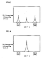
- Figures 2 to 4 are schematic views of diffraction peaks of the Si (1-v-w-x )C w Al x N v layer according to the present embodiment measured by an XRD method.
- the Si (1-v-w-x )C w Al x N v layer 12 has a diffraction peak between a SiC diffraction peak and an AlN diffraction peak as determined by the XRD method.
- the diffraction peaks of the materials as determined by the XRD method have their inherent values.
- the tube voltage is 45 kV
- the tube current is 40 mA
- the measurement mode is 20 - ⁇
- the angular resolution is 0.001 degree step
- the diffraction peak of an AlN (002) plane appears at approximately 36.03 degrees
- the diffraction peak of a SiC (102) plane appears at approximately 35.72 degrees.
- the diffraction peak between the SiC diffraction peak and the AlN diffraction peak in the Si (1-v-w-x) C w Al x N v layer 12 is higher than the SiC and AlN diffraction peaks in Fig. 2 and is lower than the SiC and AlN diffraction peaks in Fig. 3 .
- the Si (1-v-w-x )C w Al x N v layer 12 may have only a diffraction peak between the SiC diffraction peak and the AIN diffraction peak without the SiC and AlN diffraction peaks.
- the diffraction peak between the SiC diffraction peak and the AlN diffraction peak in the Si (1-v-w-x )C w Al x N v layer 12 has such a height that the diffraction peak is not a noise peak, indicating the presence of a mixed crystal of Si, C, Al, and N.
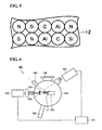
- Figure 5 is a schematic view of the arrangement of atoms constituting the Si (1-v-w- x)CwAlxNv layer according to the present embodiment.
- Si is chemically stable as SiC and therefore easily bonds to C and rarely bonds to N.
- Al is chemically stable as AlN and therefore easily bonds to N and rarely bonds to C.
- the Si (1-v-w-x) C w Al x N v layer 12 does not aggregate as SiC and AlN, and Si, Al, C, and N are dispersed at the atomic level.
- the numbers of cracks each having a size of 1 mm or more in an area 10 mm square of the Si (1-v-w-x) C w Al x N v layer 12 are seven or less for 1 > v + x > 0.5, five or less for 0.5 ⁇ v + x > 0.1, and three or less for 0.1 ⁇ v + x > 0, wherein v + x denotes the molar ratio of AIN.
- cracks each having a size of 1 mm or more refers to the total length of one continuous crack in the longitudinal direction.
- Figure 6 is a schematic view of a PLD apparatus for use in the manufacture of the Si (1-v-w-x) C w Al x N v substrate according to the present embodiment.
- the PLD apparatus 100 includes a vacuum chamber 101, a laser source 102, a raw material 103, a stage 104, a pulse motor 105, a substrate holder 106, a heater (not shown), a controller 107, a reflection high energy electron diffractometer (RHEED) 108, and a gas-supply unit 109.
- a vacuum chamber 101 a laser source 102, a raw material 103, a stage 104, a pulse motor 105, a substrate holder 106, a heater (not shown), a controller 107, a reflection high energy electron diffractometer (RHEED) 108, and a gas-supply unit 109.
- RHEED reflection high energy electron diffractometer
- the laser source 102 is disposed outside the vacuum chamber 101.
- the laser source 102 can emit a laser beam.
- the target raw material 103 can be placed in the vacuum chamber 101 such that the raw material 103 can be irradiated with a laser beam from the laser source 102.
- the raw material 103 can be mounted on the stage 104.
- the pulse motor 105 can drive the stage 104.
- the substrate holder 106 can hold the Si base substrate 11 as a base substrate.
- the heater heats the Si base substrate 11 in the substrate holder 106.
- the controller 107 can control the operation of the laser source 102 and the pulse motor 105.
- the RHEED 108 can monitor oscillations to determine the thickness of the Si (1-v-w-x) C w Al x N v layer 12 grown on the Si base substrate 11.
- the gas-supply unit 109 can supply a gas into the vacuum chamber 101.
- the PLD apparatus 100 may include other components. However, for convenience of explanation, these components are not illustrated or described.
- the raw material 103 for the Si (1-v-w-x) C w Al x N v layer 12 is prepared.
- the raw material 103 is a sintered compact of a mixture of SiC and AIN.
- the composition v + x of the Si (1-v-w-x) C w Al x N v layer 12 can depend on the molar ratio of SiC to AIN in the raw material 103.
- the raw material 103 thus prepared is placed on the stage 104 in Fig. 6 .
- the Si base substrate 11 is placed on the surface of the substrate holder 106 in the vacuum chamber 101 such that the Si base substrate 11 faces the raw material 103.
- the surface of the Si base substrate 11 is then heated to a temperature, for example, below 550°C.
- the surface temperature of the Si base substrate 11 is preferably below 550°C, more preferably 540°C or less. This heating is performed, for example, with a heater.
- a method for heating the Si base substrate 11 is not limited to a heater and may be another method, for example, the application of an electric current.
- the raw material 103 is then irradiated with a laser beam from the laser source 102.
- the laser may be krypton fluoride (KrF) excimer laser having an emission wavelength of 248 nm, a pulse repetition frequency of 10 Hz, and a pulse energy in the range of 1 to 3 J/shot.
- KrF krypton fluoride
- Another laser such as argon fluoride (ArF) excimer laser having an emission wavelength of 193 nm, may also be used.
- the vacuum chamber 101 can be evacuated to a pressure in the range of approximately 1.33 x 10 -1 to 1.33 x 10 -4 Pa (1 x 10 -3 to 1 x 10 -6 Torr) or less, for example.
- the vacuum chamber 101 is then filled with an inert gas, such as argon (Ar), or nitrogen from the gas-supply unit 109.
- the nitrogen atmosphere in the vacuum chamber 101 can supply nitrogen during the growth of the Si (1-v-w-x) C w Al x N v layer 12.
- the raw material 103 is used in the growth of the Si (1-v-w-x) C w Al x N v layer 12. This facilitates the control of v + x.
- the raw material 103 is preferably irradiated with a laser beam having a short wavelength as described above.
- a short-wavelength laser beam increases the absorption coefficient, allowing most of the laser beam to be absorbed in the vicinity of the surface of the raw material 103. This can markedly increase the surface temperature of the raw material 103, generating ablation plasma (plume) in the vacuum chamber 101.
- Ablation plasma is plasma accompanied by explosive particle emission from a solid. Ablation particles in the plasma move to the Si base substrate 11 while the state of the ablation particles alters by recombination, collision with ambient gas, a reaction, or the like. The particles reaching the Si base substrate 11 diffuse over the Si base substrate 11 and enter acceptor sites to form the Si (1-v-w-x) C w Al x N v layer 12.
- the acceptor site for an Al atom is a C or N atom binding site.
- the acceptor site for a Si atom is a C or N atom binding site.
- the acceptor site for a C atom is an Al or Si atom binding site.
- the acceptor site for a N atom is an Al or Si atom binding site.
- the thickness of the Si (1-v-w-x) C w Al x N v layer 12 to be grown can be monitored through the oscillation of the RHEED 108 installed on the vacuum chamber 101.
- the Si (1-v-w-x) C w Al x N v layer 12 can be grown on the Si base substrate 11 by a PLD method to manufacture the Si (1-v-w-x) C w Al x N v substrate 10a illustrated in Fig. 1 .
- a method for manufacturing a Si (1-v-w-x) C w Al x N v substrate 10a includes the steps of preparing the Si base substrate 11 and growing the Si (1-v-w-x) C w Al x N v layer 12 (0 ⁇ v ⁇ 1, 0 ⁇ w ⁇ 1, 0 ⁇ x ⁇ 1, and 0 ⁇ v + w + x ⁇ 1) on the Si base substrate 11 by a PLD method.
- the Si (1-v-w-x) C w Al x N v layer 12 is grown by a PLD method.
- the raw material 103 for the Si (1-v-w-x) C w Al x N v layer 12 can be irradiated with a laser beam to generate plasma.
- the plasma can be supplied onto the Si base substrate 11.
- the Si (1-v-w-x) C w Al x N v layer 12 can be grown in a non-equilibrium state. Unlike the equilibrium state, this non-equilibrium state is not a stable state.
- Si can therefore bond to C and N, and Al can bond to C and N.
- the Si (1-v-w-x) C w Al x N v layer 12 formed of a mixed crystal of four elements Si, C, Al, and N as illustrated in Fig. 5 can be grown.
- the Si base substrate 11 is used as a base substrate for the Si (1-v-w-x) C w Al x N v layer 12.
- the Si base substrate 11 is the most commonly used electronic material, and therefore processing techniques, such as etching, have been established for the Si base substrate 11.
- the Si base substrate 11 can be easily cleaved and easily etched with an acid. It is therefore easy to reduce the thickness of the S base i substrate 11 or remove the Si base substrate 11.
- the Si (1-v-w-x) C w Al x N v substrate 10a is used in the manufacture of a light-emitting device, the cleavability of the Si base substrate is very important.
- the easily processable Si (1-v-w-x) C w Al x N v substrate 10a can be manufactured.
- the Si base substrate 11 is used as a base substrate.
- the Si base substrate 11 is less expensive than SiC substrates and sapphire substrates. This can reduce the manufacturing costs of the Si (1-v-w-x) C w Al x N v substrate 10a.
- the method for growing a Si (1-v-w-x) C w Al x N v substrate 10a according to the present embodiment in which a Si (1-v-w-x) C w Al x N v layer 12 is grown by a PLD method can provide a Si (1-v-w-x) C w Al x N v substrate 10a including a Si (1-v-w-x) C w Al x N v layer 12 having a diffraction peak between a SiC diffraction peak and an AIN diffraction peak as determined by an XRD method.
- Figure 12 is a schematic view of the diffraction peaks of a Si (1-v-w-x) C w Al x N v layer grown in an equilibrium state measured by an XRD method. More specifically, Fig. 12 is a schematic view of the diffraction peaks of a (SiC) (1-x) (AlN) x layer 112 illustrated in Fig. 10 or 11 as determined by an XRD method. As illustrated in Figs.
- the (SiC)( 1-x )(AlN) x layer 112 grown in an equilibrium state, for example, by a sublimation method or a MBE method does not have a mixed crystal state of four elements Si, C, Al, and N.
- a SiC diffraction peak and an AIN diffraction peak are observed, no diffraction peak is observed between the SiC diffraction peak and the AIN diffraction peak.
- a diffraction peak within the limits of error, such as noise, may be observed between the SiC diffraction peak and the AlN diffraction peak.
- the Si (1-v-w-x) C w Al x N v layer 12 grown by the PLD method can be the Si (1-v-w-x) C w Al x N v layer 12 in a mixed crystal state of four elements Si, C, Al, and N, as illustrated in Fig. 5 .
- the Si (1-v-w-x) C w Al x N v substrate 10a including the Si (1-v-w-x) C w Al x N v layer 12 that has a diffraction peak between the SiC diffraction peak and the AIN diffraction peak as determined by an XRD method, as illustrated in Figs. 2 to 4 , can be manufactured.
- the Si (1-v-w-x) C w Al x N v substrate 10a manufactured by a method for manufacturing a Si (1-v-w-x) C w Al x N v substrate 10a according to the present embodiment can therefore be easily processed and has improved uniformity of crystal.
- the Si (1-v-w-x) C w Al x N v substrate 10a can be suitably used in various functional devices that utilize the magnetoresistance effect, such as tunneling magnetoresistive devices and giant magnetoresistive devices; light-emitting devices, such as light-emitting diodes and laser diodes; electronic devices, such as rectifiers, bipolar transistors, field-effect transistors (FETs), spin FETs, and high-electron-mobility transistors (HEMTs); semiconductor sensors, such as temperature sensors, pressure sensors, radiation sensors, and visible-ultraviolet light detectors; and SAW devices.
- magnetoresistance effect such as tunneling magnetoresistive devices and giant magnetoresistive devices
- light-emitting devices such as light-emitting diodes and laser diodes
- electronic devices such as rectifiers, bipolar transistors, field-effect transistors (FETs), spin FETs, and high-electron-mobility transistors (HEMTs)
- semiconductor sensors such as temperature sensors
- the Si (1-v-w-x) C w Al x N v layer 12 is preferably grown at a temperature below 550°C in the growing step.
- the present inventor found that the growth of the Si (1-v-w-x) C w Al x N v layer 12 at a temperature below 550°C can reduce the stress arising in the Si (1-v-w-x) C w Al x N v layer 12 due to a difference in thermal expansion coefficient between the Si (1-v-w-x) C w Al x N v layer 12 and the Si base substrate 11 while the Si (l-v-w-x) C w Al x N v layer 12 is cooled to room temperature after the growth of the Si (1-v-w-x) C w Al x N v layer 12.
- the present inventor found that the stress arising in the Si (l-v-w-x) C w Al x N v layer 12 at a growth temperature below 550°C can prevent cracks from occurring in the Si (l-v-w-x) C w Al x N v layer 12. This can reduce the number of cracks in the Si (l-v-w-x) C w Al x N v layer 12.
- the Si (1-v-w-x) C w Al x N v layer 12 is difficult to grow using the Si base substrate 11 as a base substrate because the growth temperature of the Si (1-v-w-x) C w Al x N v layer 12 is high.
- the growth of the Si (1-v-w-x) C w Al x N v layer 12 at a low temperature below 550°C can prevent the thermal degradation of the Si base substrate 11.
- the Si (1-v-w-x) C w Al x N v layer 12 can be grown on the Si base substrate 11.
- the method for growing a Si (l-v-w-x) C w Al x N v substrate 10a including growing a Si (1-v-w-x) C w Al x N v layer 12 at a temperature below 550°C can provide the Si (1-v-w-x) C w Al x N v substrate 10a having the Si (l-v-w-x) C w Al x N v layer 12 in which the numbers of cracks each having a size of 1 mm or more in an area 10 mm square of the Si (1-v-w-x) C w Al x N v layer are seven or less for 1 > v + x > 0.5, five or less for 0.5 ⁇ v + x > 0.1, and three or less for 0.1 ⁇ v + x > 0.
- Figure 7 is a schematic cross-sectional view of a Si (1-v-w-x) C w Al x N v substrate manufactured by a method according to a second embodiment of the present invention.
- a Si (l-v-w-x) C w Al x N v substrate 10b according to the present embodiment at least the Si base substrate 11 is removed from the Si (1-v-w-x) C w Al x N v substrate 10a according to the first embodiment.
- a method for manufacturing a Si (l-v-w-x) C w Al x N v substrate 10b according to the present embodiment will be described below.
- the Si (1-v-w-x) C w Al x N v substrate 10a illustrated in Fig. 1 is manufactured by the method for manufacturing a Si (l-v-w-x) C w Al x N v substrate 10a according to the first embodiment.
- the Si base substrate 11 is then removed. Only the Si base substrate 11 may be removed, or the Si base substrate 11 and part of the Si (1-v-w-x) C w Al x N v layer 12 including the surface in contact with the Si base substrate 11 may be removed.
- the removal can be performed by any method, for example, chemical removal, such as etching, or mechanical removal, such as cutting, grinding, or cleavage.
- Cutting refers to the mechanical removal of at least the Si base substrate 11 from the Si (1-v-w-x) C w Al x N v layer 12 with a slicer having a peripheral cutting edge of an electrodeposited diamond wheel.
- Grinding refers to applying a rotating whetstone to a surface to scrape the surface in the thickness direction.
- Cleavage refers to cleaving the Si base substrate 11 along the crystal lattice plane.
- a method for manufacturing a Si (1-v-w-x) C w Al x N v substrate 10b further includes the step of removing the Si base substrate 11. Since the Si base substrate 11 can be easily removed, the Si (1-v-w-x) C w Al x N v substrate 10b, for example, including the Si (1-v-w-x) C w Al x N v layer 12 alone can be easily manufactured.
- Figure 8 is a schematic cross-sectional view of an epitaxial wafer manufactured by the method according to the present embodiment.
- An epitaxial wafer 20a according to the present embodiment will be described below with reference to Fig. 8 .
- the epitaxial wafer 20a includes the Si (1-v-w-x) C w Al x N v substrate 10a according to the first embodiment and an Al (1-y-z) Ga y In z N (0 ⁇ y ⁇ 1, 0 ⁇ z ⁇ 1, and 0 ⁇ y + z ⁇ 1) layer 21 formed on the Si (l-v-w-x) C w Al x N v substrate 10a.
- the epitaxial wafer 20a includes the Si base substrate 11, the Si (1-v-w-x) C w Al x N v layer 12 formed on the Si base substrate 11, and the Al (1-y-z) Ga y ln z N layer 21 formed on the Si (1-v-w-x) C w Al x N v layer 12.
- a method for manufacturing an epitaxial wafer 20a according to the present embodiment will be described below.
- the Si (1-v-w-x) C w Al x N v substrate 10a is manufactured by the method for manufacturing a Si (1-v-w-x) C w Al x N v substrate 10a according to the first embodiment.
- the Al (1-y-z) Ga y In z N layer 21 is then grown on the Si (l-v-w-x) C w Al x N v substrate 10a (the Si (l-v-w-x) C w Al x N v layer 12 in the present embodiment).
- the growth method include, but not limited to, vapor phase epitaxy methods, such as an MOCVD method, a hydride vapor phase epitaxy (HVPE) method, an MBE method, and a sublimation method, and liquid phase epitaxy methods.
- the epitaxial wafer 20a illustrated in Fig. 8 can be manufactured.
- a step of removing the Si base substrate 11 from the epitaxial wafer 20a may be further performed.
- the Al (1-y-z) Ga y In z N layer 21 is formed on the Si (l-v-w-x) C w Al x N v substrate 10a.
- the Si (1-v-w-x) C w Al x N y substrate 10a includes the Si (1-v-w-x) C w Al x N v layer 12 in a mixed crystal state.
- An Al (1-y-z) Ga y In z N layer 21 having uniform crystallinity can therefore be grown on the Si (1-v-w-x) C w Al x N v layer 12.
- the Al (1-y-z) Ga y In z N layer 21 can have improved crystallinity.
- the Si base substrate 11 since the Si base substrate 11 can be easily processed, the Si base substrate 11 can be easily removed from the epitaxial wafer.
- Figure 9 is a schematic cross-sectional view of an epitaxial wafer according to the present embodiment.
- An epitaxial wafer 20b according to the present embodiment will be described below with reference to Fig. 9 .
- the epitaxial wafer 20b includes the Si (1-v-w-x) C w Al x N v substrate 10b according to the second embodiment and an Al (1-y-z) Ga y In z N (0 ⁇ y ⁇ 1, 0 ⁇ z ⁇ 1, and 0 ⁇ y + z ⁇ 1) layer 21 formed on the Si (1-v-w-x) C w Al x N v substrate 10b.
- the epitaxial wafer 20b includes the Si (l-v-w-x) C w Al x N v layer 12 and the Al (1-y-z) Ga y In z N layer 21 formed on the Si (l-v-w-x) C w Al x N v layer 12.
- a method for manufacturing an epitaxial wafer 20b according to the present embodiment will be described below.
- the Si (l-v-w-x) C w Al x N v substrate 10b is manufactured by the method for manufacturing a Si (l-v-w-x) C w Al x N v substrate 10b according to the second embodiment.
- the Al (1-y-z) Ga y In z N layer 21 is then grown on the Si (l-v-w-x) C w Al x N v substrate 10b (the Si (l-v-w-x) C w Al x N v layer 12 in the present embodiment) as in the third embodiment.
- the epitaxial wafer 20b illustrated in Fig. 9 can be manufactured.
- the Al (1-y-z) Ga y In z N layer 21 is formed on the Si (l-v-w-x) C w Al x N v substrate 10b. Since the Si (1-v-w-x) C w Al x N v substrate 10b includes the Si (1-v-w-x) C w Al x N v layer 12 in a mixed crystal state, the Al (1-y-z) Ga y In z N layer 21 having uniform crystallinity can be grown.
- a Si (1-v-w-x) C w Al x N v substrate 10a was basically manufactured by the method for manufacturing a Si (l-v-w-x) C w Al x N v substrate 10a according to the first embodiment with a PLD apparatus illustrated in Fig. 6 .
- Si 0.05 C 0.05 (AlN) 0.9 wherein v+ x was 0.9 was produced as a Si (1-v-w-x) C w Al x N v layer 12.
- the raw material 103 for a Si 0.05 C 0.05 (AlN) 0.9 layer 12 was first prepared.
- the raw material 103 was prepared in the following way. More specifically, a SiC powder and an AIN powder were mixed and pressed. This mixture was placed in a vacuum vessel. After the vacuum vessel was evacuated to 1.33 x 10 -4 Pa (10 -6 Torr), the atmosphere was filled with a high-purity Ar gas. The mixture was then fired at 2300°C for 20 hours to prepare the raw material 103. The raw material 103 was placed on the stage 104 illustrated in Fig. 6 .
- a Si base substrate 11 was then prepared as a base substrate.
- the Si base substrate 11 had a (001) plane as a main surface 11a and a size of one inch.
- the Si base substrate 11 was placed on the surface of a substrate holder 106 in a vacuum chamber 101 such that the Si base substrate 11 faced the raw material 103.
- the surface of the Si base substrate 11 was then heated to a temperature of 540°C.
- the raw material 103 was then irradiated with a laser beam from a laser source 102.
- the laser was KrF excimer laser having an emission wavelength of 248 nm, a pulse repetition frequency of 10 Hz, and a pulse energy in the range of I to 3 J/shot.
- the vacuum chamber 101 was evacuated to 1.33 x 10 -4 Pa (1 x 10 -6 Torr) and was then filled with nitrogen.
- the Si 0.05 C 0.05 (AlN) 0.9 layer 12 having a thickness of 500 nm was grown while monitoring the thickness through the oscillation of a RHEED 108 installed on the vacuum chamber 101.
- a Si 0.05 C 0.05 (AlN) 0.9 substrate was manufactured basically in the same manner as in Working Example 1 except that the Si base substrate serving as a base substrate was replaced with a sapphire substrate having a (0001) main surface.
- a Si 0.05 C 0.05 (AlN) 0.9 substrate was manufactured basically in the same manner as in Working Example 1 except that the Si base substrate serving as a base substrate was replaced with a 6H-SiC substrate having a (0001) main surface.
- Table I shows the results.
- Pass means that the base substrate was successfully removed
- Fail means that the base substrate was not successfully removed.
- Base substrate HF+HNO 3 KOH Cleavability Working *) Example 1 Si(001) Pass Pass Pass Comparative Example 1 Al 2 O 3 (0001) Fail Fail Fail Comparative Example 2 6H-SiC(0001) Fail Fail Pass *) not in accordance with the invention
- Table I shows that the Si 0.05 C 0.05 (AlN) 0.9 substrate according to Working Example 1, which used the Si base substrate as the base substrate, exhibited excellent etching characteristics and cleavability of the Si base substrate. This showed that the Si base substrate could be easily processed.
- the Si 0.05 C 0.05 (AlN) 0.9 substrate according to Comparative Example 1 which used the sapphire substrate as the base substrate, exhibited poor etching characteristics and cleavability of the sapphire substrate. The sapphire substrate was therefore not sufficiently removed.
- the Si 0.05 C 0.05 (AlN) 0.9 substrate according to Comparative Example 2 which used the SiC substrate as the base substrate, exhibited poor etching characteristics of the SiC substrate. The SiC substrate was therefore not sufficiently removed by etching.
- the present example showed that a S i(1-v-w-x) C w Al x N v substrate that can be easily processed can be manufactured using a Si base substrate.
- Si 0.05 C 0.05 Al 0.45 N 0.45 was grown basically in the same manner as in Working Example 1 except that a Si base substrate 11 having a (111) main surface was used as the base substrate.
- Working Example 3 was basically the same as Working Example 2 except that the Si (1-v-w-x) C w Al x N v layer 12 grown was Si 0.0005 C 0.0005 Al 0.4994 N 0.4996 . This change was achieved by altering the molar ratio of the AIN powder to the SiC powder in the raw material 103 prepared.
- Working Example 4 was basically the same as Working Example 2 except that the Si (1-v-w-x) C w Al x N v layer 12 grown was Si 0.0005 C 0.0005 Al 0.4996 N 0.4994 .
- Working Example 5 was basically the same as Working Example 2 except that the Si (1-v-w-x) C w Al x N v layer 12 grown was Si 0.0005 C 0.0005 Al 0.4995 N 0.4995 .
- Working Example 6 was basically the same as Working Example 2 except that the Si (1-v-w-x) C w Al x N v layer 12 grown was Si 0.0006 C 0.0004 Al 0.4995 N 0.4995 .
- Working Example 7 was basically the same as Working Example 2 except that the Si (1-v-w-x) C w Al x N v layer 12 grown was Si 0.0004 C 0.0006 Al 0.4995 N 0.4995 .
- Working Example 8 was basically the same as Working Example 2 except that the Si (1-v-w-x) C w Al x N v layer 12 grown was Si 0.005 C 0.005 Al 0.495 N 0.495 .
- Working Example 9 was basically the same as Working Example 1 except that the Si (1-v-w-x) C w Al x N v layer 12 grown was Si 0.25 C 0.25 Al 0.25 N 0.25 .
- Working Example 10 was basically the same as Working Example 1 except that the Si (1-v-w-x) C w Al x N v layer 12 grown was Si 0.45 C 0.45 Al 0.05 N 0.05 .
- Working Example 11 was basically the same as Working Example 2 except that the Si (1-v-w-x) C w Al x N v layer 12 grown was Si 0.495 C 0.495 Al 0.005 N 0.005 .
- Working Example 12 was basically the same as Working Example 2 except that the Si (1-v-w-x) C w Al x N v layer 12 grown was Si 0.4995 C 0.4995 Al 0.0004 N 0.0006 .
- Working Example 13 was basically the same as Working Example 2 except that the Si (1-v-w-x) C w Al x N v layer 12 grown was Si 0.4995 C 0.4995 Al 0.0006 N 0.0004 .
- Working Example 14 was basically the same as Working Example 2 except that the Si (1-v-w-x) C w Al x N v layer 12 grown was Si 0.4995 C 0.4995 Al 0.0005 N 0.0005 .
- Working Example 15 was basically the same as Working Example 2 except that the Si (1-v-w-x) C w Al x N v layer 12 grown was Si 0.4996 C 0.4994 Al 0.0005 N 0.0005 .
- Working Example 16 was basically the same as Working Example 2 except that the Si (1-v-w-x) C w Al x N v layer 12 grown was Si 0.4994 C 0.4996 Al 0.0005 N 0.0005 .
- Working Example 17 was basically the same as Working Example 2 except that the Si 0.05 C 0.05 Al 0.45 N 0.45 layer was grown at a temperature of the main surface of the Si base substrate of 550°C.
- Working Example 18 was basically the same as Working Example 2 except that a Si 0.0005 C 0.0005 Al 0.4994 N 0.4996 layer was grown at a temperature of the main surface of the Si base substrate of 550°C.
- Working Example 19 was basically the same as Working Example 2 except that a Si 0.0005 C 0.0005 Al 0.4996 N 0.4994 layer was grown at a temperature of the main surface of the Si base substrate of 550°C.
- Working Example 20 was basically the same as Working Example 2 except that a Si 0.0005 C 0.0005 Al 0.4995 N 0.4995 layer was grown at a temperature of the main surface of the Si base substrate of 550°C.
- Working Example 21 was basically the same as Working Example 2 except that a So 0.0006 C 0.0004 Al 0.4995 N 0.4995 layer was grown at a temperature of the main surface of the Si base substrate of 550°C.
- Working Example 22 was basically the same as Working Example 2 except that a Si 0.0004 C 0.0006 Al 0.4995 N 0.4995 layer was grown at a temperature of the main surface of the Si base substrate of 550°C.
- Working Example 23 was basically the same as Working Example 2 except that a Si 0.005 C 0.005 Al 0.495 N 0.495 layer was grown at a temperature of the main surface of the Si base substrate of 550°C.
- Working Example 24 was basically the same as Working Example 2 except that a Si 0.25 C 0.25 Al 0.25 N 0.25 layer was grown at a temperature of the main surface of the Si base substrate of 550°C.
- Working Example 25 was basically the same as Working Example 2 except that a Si 0.45 C 0.45 Al 0.05 N 0.05 layer was grown at a temperature of the main surface of the Si base substrate of 550°C.
- Working Example 26 was basically the same as Working Example 2 except that a Si 0.495 C 0.495 Al 0.005 N 0.005 layer was grown at a temperature of the main surface of the Si base substrate of 550°C.
- Working Example 27 was basically the same as Working Example 2 except that a Si 0.4995 C 0.4995 Al 0.0004 N 0.0006 layer was grown at a temperature of the main surface of the Si base substrate of 550°C
- Working Example 28 was basically the same as Working Example 2 except that a Si 0.4995 C 0.4995 Al 0.0006 N 0.0004 layer was grown at a temperature of the main surface of the Si base substrate of 550°C.
- Working Example 29 was basically the same as Working Example 2 except that a Si 0.4995 C 0.4995 Al 0.0005 N 0.0005 layer was grown at a temperature of the main surface of the Si base substrate of 550°C.
- Working Example 30 was basically the same as Working Example 2 except that a Si 0.4996 C 0.4994 Al 0.0005 N 0.0005 layer was grown at a temperature of the main surface of the Si base substrate of 550°C.
- Working Example 31 was basically the same as Working Example 2 except that a Si 0.4994 C 0.4996 Al 0.0005 N 0.0005 layer was grown at a temperature of the main surface of the Si base substrate of 550°C.
- Comparative Example 3 was basically the same as Working Example 2 except that an AlN layer was grown at a temperature of the main surface of the Si base substrate of 540°C.
- Comparative Example 4 was basically the same as Working Example 2 except that an AIN layer was grown at a temperature of the main surface of the Si base substrate of 550°C.
- Comparative Example 5 was basically the same as Working Example 2 except that a SiC layer was grown at a temperature of the main surface of the Si base substrate of 540°C.
- Comparative Example 6 was basically the same as Working Example 2 except that a SiC layer was grown at a temperature of the main surface of the Si base substrate of 550°C.
- Table II shows that the number of cracks in the Si (l-v-w-x) C w Al x N v layer in which v + x was 0.9, 0.999, or 0.99 grown at 540°C in Working Examples 2 to 8 was seven. In contrast, the number of cracks in the Si (1-v-w-x) C w Al x N v layer in which v + x was 0.9, 0.999, or 0.99 grown at 550°C in Comparative Examples 17 to 23 was eight.
- the number of cracks in the Si 0.25 C 0.25 Al 0.25 N 0.25 layer grown at 540°C in Working Example 9 was five.
- the number of cracks in the Si 0.25 C 0.25 Al 0.25 N 0.25 layer, which had the same composition as in Working Example 5, grown at 550°C in Comparative Example 24 was six.
- a Si (l-v-w-x) C w Al x N v layer having a larger v + x has a larger difference in composition from the Si base substrate 11, resulting in an increased number of cracks.
- Table II shows that the numbers of cracks in a Si (l-v-w-x) C w Al x N v layer grown at 540°C were seven or less for 1 > v + x > 0.5, five or less for 0.5 ⁇ v + x > 0.1, and three or less for 0.1 ⁇ v + x > 0.
- the present example showed that a Si (1-v-w-x) C w Al x N v layer (0 ⁇ v + x ⁇ 1) grown at a temperature below 550°C can reduce the number of cracks in the Si (1-v-w-x) C w Al x N v layer (0 ⁇ v + x ⁇ 1).
Landscapes
- Chemical & Material Sciences (AREA)
- Engineering & Computer Science (AREA)
- Materials Engineering (AREA)
- Metallurgy (AREA)
- Organic Chemistry (AREA)
- Crystallography & Structural Chemistry (AREA)
- Inorganic Chemistry (AREA)
- Chemical Kinetics & Catalysis (AREA)
- Mechanical Engineering (AREA)
- Health & Medical Sciences (AREA)
- Toxicology (AREA)
- Crystals, And After-Treatments Of Crystals (AREA)
- Recrystallisation Techniques (AREA)
- Physical Vapour Deposition (AREA)
Claims (3)
- Verfahren zur Herstellung eines Si(1-v-w-x)CwAlxNv Substrats (10a), mit den Schritten:Herstellen eines Si Basissubstrats (11); undWachsen einer Si(1-v-w-x)CwAlxNv Schicht (12) (0 < v < 1, 0 < w < 1, 0 < x < 1, 0 < v + w + x < 1, und 0 < v + x ≤ 0,1) auf dem Si Basissubstrat durch eine gepulstes Laserabscheidungsverfahren.
- Verfahren zur Herstellung eines Si(1-v-w-x)CwAlxNv Substrats nach Anspruch 1, das ferner den Schritt umfasst, das Si Basissubstrat nach dem Wachstumsschritt zu entfernen.
- Verfahren zur Herstellung eines epitaktischen Wafers, mit den Schritten:Herstellen eines Si(1-v-w-x)CwAlxNv Substrats durch ein Verfahren zur Herstellung eines Si(1-v-w-x)CwAlxNv Substrats nach Anspruch 1 oder 2; undWachsen einer Al(1-y-z)GayInzN Schicht (0 ≤ y ≤ 1, 0 ≤ z ≤ 1, und 0 ≤ y + z ≤ 1) auf der Si(1-v-w-x)CwAlxNv Schicht.
Applications Claiming Priority (3)
| Application Number | Priority Date | Filing Date | Title |
|---|---|---|---|
| JP2008114467 | 2008-04-24 | ||
| JP2009056915A JP2009280903A (ja) | 2008-04-24 | 2009-03-10 | Si(1−v−w−x)CwAlxNv基材の製造方法、エピタキシャルウエハの製造方法、Si(1−v−w−x)CwAlxNv基材およびエピタキシャルウエハ |
| PCT/JP2009/057723 WO2009131064A1 (ja) | 2008-04-24 | 2009-04-17 | Si(1-v-w-x)CwAlxNv基材の製造方法、エピタキシャルウエハの製造方法、Si(1-v-w-x)CwAlxNv基材およびエピタキシャルウエハ |
Publications (3)
| Publication Number | Publication Date |
|---|---|
| EP2276060A1 EP2276060A1 (de) | 2011-01-19 |
| EP2276060A4 EP2276060A4 (de) | 2013-10-16 |
| EP2276060B1 true EP2276060B1 (de) | 2015-02-25 |
Family
ID=41216800
Family Applications (1)
| Application Number | Title | Priority Date | Filing Date |
|---|---|---|---|
| EP09733673.9A Not-in-force EP2276060B1 (de) | 2008-04-24 | 2009-04-17 | Verfahren zur herstellung eines si(1-v-w-x)cwalxnv-basismaterials und verfahren zur herstellung eines epitaxialwafers |
Country Status (6)
| Country | Link |
|---|---|
| US (2) | US8357597B2 (de) |
| EP (1) | EP2276060B1 (de) |
| JP (1) | JP2009280903A (de) |
| KR (1) | KR20100137534A (de) |
| CN (1) | CN102017080B (de) |
| WO (1) | WO2009131064A1 (de) |
Families Citing this family (4)
| Publication number | Priority date | Publication date | Assignee | Title |
|---|---|---|---|---|
| JP5621199B2 (ja) * | 2008-04-24 | 2014-11-05 | 住友電気工業株式会社 | Si(1−v−w−x)CwAlxNv基材の製造方法、エピタキシャルウエハの製造方法、Si(1−v−w−x)CwAlxNv基材およびエピタキシャルウエハ |
| JP2009280484A (ja) * | 2008-04-24 | 2009-12-03 | Sumitomo Electric Ind Ltd | Si(1−v−w−x)CwAlxNv基材の製造方法、エピタキシャルウエハの製造方法、Si(1−v−w−x)CwAlxNv基材およびエピタキシャルウエハ |
| KR101346415B1 (ko) * | 2008-08-29 | 2014-01-02 | 미쓰비시덴키 가부시키가이샤 | SiC 단결정막의 제조 방법 및 장치 |
| EP4312248A1 (de) * | 2022-07-27 | 2024-01-31 | Siltronic AG | Heteroepitaktischer wafer zur abscheidung von galliumnitrid |
Family Cites Families (17)
| Publication number | Priority date | Publication date | Assignee | Title |
|---|---|---|---|---|
| US4382837A (en) | 1981-06-30 | 1983-05-10 | International Business Machines Corporation | Epitaxial crystal fabrication of SiC:AlN |
| JPS61291495A (ja) * | 1985-06-18 | 1986-12-22 | Sharp Corp | 炭化珪素単結晶基板の製造方法 |
| JPH067594B2 (ja) | 1987-11-20 | 1994-01-26 | 富士通株式会社 | 半導体基板の製造方法 |
| JPH04167477A (ja) | 1990-10-31 | 1992-06-15 | Toshiba Corp | 半導体素子 |
| US6086672A (en) | 1998-10-09 | 2000-07-11 | Cree, Inc. | Growth of bulk single crystals of aluminum nitride: silicon carbide alloys |
| US6911084B2 (en) * | 2001-09-26 | 2005-06-28 | Arizona Board Of Regents | Low temperature epitaxial growth of quaternary wide bandgap semiconductors |
| KR20040058206A (ko) * | 2001-10-16 | 2004-07-03 | 아리조나 보드 오브 리전트스, 아리조나주의 아리조나 주립대 대행법인 | 4원 광 밴드갭 반도체의 저온 에피택셜 성장 |
| WO2004073045A2 (en) | 2003-02-12 | 2004-08-26 | Arizona Board Of Regents, A Body Corporate Of The State Of Arizona, Acting For And On Behalf Of Arizona State University | Epitaxial growth of a zirconium diboride layer on silicon substrates |
| US7250648B2 (en) | 2003-09-04 | 2007-07-31 | Intematix Corporation | Ferroelectric rare-earth manganese-titanium oxides |
| KR100659579B1 (ko) * | 2004-12-08 | 2006-12-20 | 한국전자통신연구원 | 발광 소자 및 발광 소자의 제조방법 |
| WO2007049939A1 (en) | 2005-10-29 | 2007-05-03 | Samsung Electronics Co., Ltd. | Semiconductor device and method of fabricating the same |
| US7371282B2 (en) | 2006-07-12 | 2008-05-13 | Northrop Grumman Corporation | Solid solution wide bandgap semiconductor materials |
| CN100588737C (zh) * | 2007-03-30 | 2010-02-10 | 中国科学院上海硅酸盐研究所 | 一种p型含铜硫透明导体薄膜的制备方法 |
| US20080277778A1 (en) * | 2007-05-10 | 2008-11-13 | Furman Bruce K | Layer Transfer Process and Functionally Enhanced Integrated Circuits Products Thereby |
| JP5621199B2 (ja) * | 2008-04-24 | 2014-11-05 | 住友電気工業株式会社 | Si(1−v−w−x)CwAlxNv基材の製造方法、エピタキシャルウエハの製造方法、Si(1−v−w−x)CwAlxNv基材およびエピタキシャルウエハ |
| JP2009280484A (ja) * | 2008-04-24 | 2009-12-03 | Sumitomo Electric Ind Ltd | Si(1−v−w−x)CwAlxNv基材の製造方法、エピタキシャルウエハの製造方法、Si(1−v−w−x)CwAlxNv基材およびエピタキシャルウエハ |
| US8247249B2 (en) | 2010-06-01 | 2012-08-21 | Palo Alto Research Center Incorporated | Semi-polar nitride-based light emitting structure and method of forming same |
-
2009
- 2009-03-10 JP JP2009056915A patent/JP2009280903A/ja active Pending
- 2009-04-17 US US12/989,039 patent/US8357597B2/en not_active Expired - Fee Related
- 2009-04-17 EP EP09733673.9A patent/EP2276060B1/de not_active Not-in-force
- 2009-04-17 WO PCT/JP2009/057723 patent/WO2009131064A1/ja not_active Ceased
- 2009-04-17 CN CN200980114395.5A patent/CN102017080B/zh not_active Expired - Fee Related
- 2009-04-17 KR KR1020107023484A patent/KR20100137534A/ko not_active Abandoned
-
2012
- 2012-12-14 US US13/715,254 patent/US8937339B2/en not_active Expired - Fee Related
Also Published As
| Publication number | Publication date |
|---|---|
| JP2009280903A (ja) | 2009-12-03 |
| EP2276060A1 (de) | 2011-01-19 |
| CN102017080A (zh) | 2011-04-13 |
| US20130105858A1 (en) | 2013-05-02 |
| US8357597B2 (en) | 2013-01-22 |
| CN102017080B (zh) | 2013-04-24 |
| EP2276060A4 (de) | 2013-10-16 |
| WO2009131064A1 (ja) | 2009-10-29 |
| US8937339B2 (en) | 2015-01-20 |
| US20110042788A1 (en) | 2011-02-24 |
| KR20100137534A (ko) | 2010-12-30 |
Similar Documents
| Publication | Publication Date | Title |
|---|---|---|
| US11913136B2 (en) | Thermal control for formation and processing of aluminum nitride | |
| US12264410B2 (en) | Aluminum nitride crystals having low urbach energy and high transparency to deep-ultraviolet wavelengths | |
| US9650723B1 (en) | Large area seed crystal for ammonothermal crystal growth and method of making | |
| US8715414B2 (en) | Process for producing Si(1-v-w-x)CwAlxNv base material, process for producing epitaxial wafer, Si(1-v-w-x)CwAlxNv base material, and epitaxial wafer | |
| EP2276060B1 (de) | Verfahren zur herstellung eines si(1-v-w-x)cwalxnv-basismaterials und verfahren zur herstellung eines epitaxialwafers | |
| EP2302110B1 (de) | Verfahren zur herstellung eines si(1-v-w-x)cwalxnv-substrats, verfahren zur herstellung eines epitaktischen wafers, si(1-v-w-x)cwalxnv-substrat und epitaktischer wafer | |
| KR20130025629A (ko) | 박막 성장방법 |
Legal Events
| Date | Code | Title | Description |
|---|---|---|---|
| PUAI | Public reference made under article 153(3) epc to a published international application that has entered the european phase |
Free format text: ORIGINAL CODE: 0009012 |
|
| 17P | Request for examination filed |
Effective date: 20101020 |
|
| AK | Designated contracting states |
Kind code of ref document: A1 Designated state(s): AT BE BG CH CY CZ DE DK EE ES FI FR GB GR HR HU IE IS IT LI LT LU LV MC MK MT NL NO PL PT RO SE SI SK TR |
|
| AX | Request for extension of the european patent |
Extension state: AL BA RS |
|
| DAX | Request for extension of the european patent (deleted) | ||
| REG | Reference to a national code |
Ref country code: DE Ref legal event code: R079 Ref document number: 602009029545 Country of ref document: DE Free format text: PREVIOUS MAIN CLASS: H01L0021205000 Ipc: C30B0029380000 |
|
| A4 | Supplementary search report drawn up and despatched |
Effective date: 20130912 |
|
| RIC1 | Information provided on ipc code assigned before grant |
Ipc: C30B 29/36 20060101ALI20130906BHEP Ipc: C30B 29/40 20060101ALI20130906BHEP Ipc: C30B 23/08 20060101ALI20130906BHEP Ipc: C30B 25/02 20060101ALI20130906BHEP Ipc: H01L 29/267 20060101ALI20130906BHEP Ipc: C23C 14/28 20060101ALI20130906BHEP Ipc: C30B 29/38 20060101AFI20130906BHEP Ipc: C30B 23/02 20060101ALI20130906BHEP Ipc: C23C 14/06 20060101ALI20130906BHEP Ipc: H01L 21/02 20060101ALI20130906BHEP |
|
| 17Q | First examination report despatched |
Effective date: 20140502 |
|
| GRAP | Despatch of communication of intention to grant a patent |
Free format text: ORIGINAL CODE: EPIDOSNIGR1 |
|
| INTG | Intention to grant announced |
Effective date: 20140919 |
|
| GRAS | Grant fee paid |
Free format text: ORIGINAL CODE: EPIDOSNIGR3 |
|
| GRAA | (expected) grant |
Free format text: ORIGINAL CODE: 0009210 |
|
| AK | Designated contracting states |
Kind code of ref document: B1 Designated state(s): AT BE BG CH CY CZ DE DK EE ES FI FR GB GR HR HU IE IS IT LI LT LU LV MC MK MT NL NO PL PT RO SE SI SK TR |
|
| REG | Reference to a national code |
Ref country code: GB Ref legal event code: FG4D |
|
| REG | Reference to a national code |
Ref country code: CH Ref legal event code: EP |
|
| REG | Reference to a national code |
Ref country code: IE Ref legal event code: FG4D |
|
| REG | Reference to a national code |
Ref country code: DE Ref legal event code: R096 Ref document number: 602009029545 Country of ref document: DE Effective date: 20150402 |
|
| REG | Reference to a national code |
Ref country code: AT Ref legal event code: REF Ref document number: 712093 Country of ref document: AT Kind code of ref document: T Effective date: 20150415 |
|
| REG | Reference to a national code |
Ref country code: NL Ref legal event code: VDEP Effective date: 20150225 |
|
| REG | Reference to a national code |
Ref country code: AT Ref legal event code: MK05 Ref document number: 712093 Country of ref document: AT Kind code of ref document: T Effective date: 20150225 |
|
| REG | Reference to a national code |
Ref country code: LT Ref legal event code: MG4D |
|
| PG25 | Lapsed in a contracting state [announced via postgrant information from national office to epo] |
Ref country code: ES Free format text: LAPSE BECAUSE OF FAILURE TO SUBMIT A TRANSLATION OF THE DESCRIPTION OR TO PAY THE FEE WITHIN THE PRESCRIBED TIME-LIMIT Effective date: 20150225 Ref country code: SE Free format text: LAPSE BECAUSE OF FAILURE TO SUBMIT A TRANSLATION OF THE DESCRIPTION OR TO PAY THE FEE WITHIN THE PRESCRIBED TIME-LIMIT Effective date: 20150225 Ref country code: FI Free format text: LAPSE BECAUSE OF FAILURE TO SUBMIT A TRANSLATION OF THE DESCRIPTION OR TO PAY THE FEE WITHIN THE PRESCRIBED TIME-LIMIT Effective date: 20150225 Ref country code: HR Free format text: LAPSE BECAUSE OF FAILURE TO SUBMIT A TRANSLATION OF THE DESCRIPTION OR TO PAY THE FEE WITHIN THE PRESCRIBED TIME-LIMIT Effective date: 20150225 Ref country code: NO Free format text: LAPSE BECAUSE OF FAILURE TO SUBMIT A TRANSLATION OF THE DESCRIPTION OR TO PAY THE FEE WITHIN THE PRESCRIBED TIME-LIMIT Effective date: 20150525 Ref country code: LT Free format text: LAPSE BECAUSE OF FAILURE TO SUBMIT A TRANSLATION OF THE DESCRIPTION OR TO PAY THE FEE WITHIN THE PRESCRIBED TIME-LIMIT Effective date: 20150225 |
|
| PG25 | Lapsed in a contracting state [announced via postgrant information from national office to epo] |
Ref country code: AT Free format text: LAPSE BECAUSE OF FAILURE TO SUBMIT A TRANSLATION OF THE DESCRIPTION OR TO PAY THE FEE WITHIN THE PRESCRIBED TIME-LIMIT Effective date: 20150225 Ref country code: IS Free format text: LAPSE BECAUSE OF FAILURE TO SUBMIT A TRANSLATION OF THE DESCRIPTION OR TO PAY THE FEE WITHIN THE PRESCRIBED TIME-LIMIT Effective date: 20150625 Ref country code: GR Free format text: LAPSE BECAUSE OF FAILURE TO SUBMIT A TRANSLATION OF THE DESCRIPTION OR TO PAY THE FEE WITHIN THE PRESCRIBED TIME-LIMIT Effective date: 20150526 Ref country code: LV Free format text: LAPSE BECAUSE OF FAILURE TO SUBMIT A TRANSLATION OF THE DESCRIPTION OR TO PAY THE FEE WITHIN THE PRESCRIBED TIME-LIMIT Effective date: 20150225 |
|
| PG25 | Lapsed in a contracting state [announced via postgrant information from national office to epo] |
Ref country code: NL Free format text: LAPSE BECAUSE OF FAILURE TO SUBMIT A TRANSLATION OF THE DESCRIPTION OR TO PAY THE FEE WITHIN THE PRESCRIBED TIME-LIMIT Effective date: 20150225 |
|
| PG25 | Lapsed in a contracting state [announced via postgrant information from national office to epo] |
Ref country code: EE Free format text: LAPSE BECAUSE OF FAILURE TO SUBMIT A TRANSLATION OF THE DESCRIPTION OR TO PAY THE FEE WITHIN THE PRESCRIBED TIME-LIMIT Effective date: 20150225 Ref country code: DK Free format text: LAPSE BECAUSE OF FAILURE TO SUBMIT A TRANSLATION OF THE DESCRIPTION OR TO PAY THE FEE WITHIN THE PRESCRIBED TIME-LIMIT Effective date: 20150225 Ref country code: RO Free format text: LAPSE BECAUSE OF FAILURE TO SUBMIT A TRANSLATION OF THE DESCRIPTION OR TO PAY THE FEE WITHIN THE PRESCRIBED TIME-LIMIT Effective date: 20150225 Ref country code: SK Free format text: LAPSE BECAUSE OF FAILURE TO SUBMIT A TRANSLATION OF THE DESCRIPTION OR TO PAY THE FEE WITHIN THE PRESCRIBED TIME-LIMIT Effective date: 20150225 Ref country code: CZ Free format text: LAPSE BECAUSE OF FAILURE TO SUBMIT A TRANSLATION OF THE DESCRIPTION OR TO PAY THE FEE WITHIN THE PRESCRIBED TIME-LIMIT Effective date: 20150225 |
|
| REG | Reference to a national code |
Ref country code: DE Ref legal event code: R097 Ref document number: 602009029545 Country of ref document: DE |
|
| PG25 | Lapsed in a contracting state [announced via postgrant information from national office to epo] |
Ref country code: LU Free format text: LAPSE BECAUSE OF FAILURE TO SUBMIT A TRANSLATION OF THE DESCRIPTION OR TO PAY THE FEE WITHIN THE PRESCRIBED TIME-LIMIT Effective date: 20150417 Ref country code: PL Free format text: LAPSE BECAUSE OF FAILURE TO SUBMIT A TRANSLATION OF THE DESCRIPTION OR TO PAY THE FEE WITHIN THE PRESCRIBED TIME-LIMIT Effective date: 20150225 Ref country code: MC Free format text: LAPSE BECAUSE OF FAILURE TO SUBMIT A TRANSLATION OF THE DESCRIPTION OR TO PAY THE FEE WITHIN THE PRESCRIBED TIME-LIMIT Effective date: 20150225 |
|
| REG | Reference to a national code |
Ref country code: CH Ref legal event code: PL |
|
| PG25 | Lapsed in a contracting state [announced via postgrant information from national office to epo] |
Ref country code: IT Free format text: LAPSE BECAUSE OF FAILURE TO SUBMIT A TRANSLATION OF THE DESCRIPTION OR TO PAY THE FEE WITHIN THE PRESCRIBED TIME-LIMIT Effective date: 20150225 |
|
| PLBE | No opposition filed within time limit |
Free format text: ORIGINAL CODE: 0009261 |
|
| STAA | Information on the status of an ep patent application or granted ep patent |
Free format text: STATUS: NO OPPOSITION FILED WITHIN TIME LIMIT |
|
| GBPC | Gb: european patent ceased through non-payment of renewal fee |
Effective date: 20150525 |
|
| REG | Reference to a national code |
Ref country code: IE Ref legal event code: MM4A |
|
| PG25 | Lapsed in a contracting state [announced via postgrant information from national office to epo] |
Ref country code: LI Free format text: LAPSE BECAUSE OF NON-PAYMENT OF DUE FEES Effective date: 20150430 Ref country code: CH Free format text: LAPSE BECAUSE OF NON-PAYMENT OF DUE FEES Effective date: 20150430 |
|
| 26N | No opposition filed |
Effective date: 20151126 |
|
| PG25 | Lapsed in a contracting state [announced via postgrant information from national office to epo] |
Ref country code: SI Free format text: LAPSE BECAUSE OF FAILURE TO SUBMIT A TRANSLATION OF THE DESCRIPTION OR TO PAY THE FEE WITHIN THE PRESCRIBED TIME-LIMIT Effective date: 20150225 |
|
| REG | Reference to a national code |
Ref country code: FR Ref legal event code: PLFP Year of fee payment: 8 |
|
| PG25 | Lapsed in a contracting state [announced via postgrant information from national office to epo] |
Ref country code: GB Free format text: LAPSE BECAUSE OF NON-PAYMENT OF DUE FEES Effective date: 20150525 Ref country code: IE Free format text: LAPSE BECAUSE OF NON-PAYMENT OF DUE FEES Effective date: 20150417 |
|
| PG25 | Lapsed in a contracting state [announced via postgrant information from national office to epo] |
Ref country code: BE Free format text: LAPSE BECAUSE OF FAILURE TO SUBMIT A TRANSLATION OF THE DESCRIPTION OR TO PAY THE FEE WITHIN THE PRESCRIBED TIME-LIMIT Effective date: 20150225 |
|
| PG25 | Lapsed in a contracting state [announced via postgrant information from national office to epo] |
Ref country code: MT Free format text: LAPSE BECAUSE OF FAILURE TO SUBMIT A TRANSLATION OF THE DESCRIPTION OR TO PAY THE FEE WITHIN THE PRESCRIBED TIME-LIMIT Effective date: 20150225 |
|
| REG | Reference to a national code |
Ref country code: FR Ref legal event code: PLFP Year of fee payment: 9 |
|
| PGFP | Annual fee paid to national office [announced via postgrant information from national office to epo] |
Ref country code: FR Payment date: 20170313 Year of fee payment: 9 |
|
| PG25 | Lapsed in a contracting state [announced via postgrant information from national office to epo] |
Ref country code: BG Free format text: LAPSE BECAUSE OF FAILURE TO SUBMIT A TRANSLATION OF THE DESCRIPTION OR TO PAY THE FEE WITHIN THE PRESCRIBED TIME-LIMIT Effective date: 20150225 Ref country code: HU Free format text: LAPSE BECAUSE OF FAILURE TO SUBMIT A TRANSLATION OF THE DESCRIPTION OR TO PAY THE FEE WITHIN THE PRESCRIBED TIME-LIMIT; INVALID AB INITIO Effective date: 20090417 |
|
| PG25 | Lapsed in a contracting state [announced via postgrant information from national office to epo] |
Ref country code: CY Free format text: LAPSE BECAUSE OF FAILURE TO SUBMIT A TRANSLATION OF THE DESCRIPTION OR TO PAY THE FEE WITHIN THE PRESCRIBED TIME-LIMIT Effective date: 20150225 |
|
| PG25 | Lapsed in a contracting state [announced via postgrant information from national office to epo] |
Ref country code: PT Free format text: LAPSE BECAUSE OF FAILURE TO SUBMIT A TRANSLATION OF THE DESCRIPTION OR TO PAY THE FEE WITHIN THE PRESCRIBED TIME-LIMIT Effective date: 20150625 |
|
| PG25 | Lapsed in a contracting state [announced via postgrant information from national office to epo] |
Ref country code: TR Free format text: LAPSE BECAUSE OF FAILURE TO SUBMIT A TRANSLATION OF THE DESCRIPTION OR TO PAY THE FEE WITHIN THE PRESCRIBED TIME-LIMIT Effective date: 20150225 |
|
| PG25 | Lapsed in a contracting state [announced via postgrant information from national office to epo] |
Ref country code: MK Free format text: LAPSE BECAUSE OF FAILURE TO SUBMIT A TRANSLATION OF THE DESCRIPTION OR TO PAY THE FEE WITHIN THE PRESCRIBED TIME-LIMIT Effective date: 20150225 |
|
| PG25 | Lapsed in a contracting state [announced via postgrant information from national office to epo] |
Ref country code: FR Free format text: LAPSE BECAUSE OF NON-PAYMENT OF DUE FEES Effective date: 20180430 |
|
| P01 | Opt-out of the competence of the unified patent court (upc) registered |
Effective date: 20230515 |
|
| PGFP | Annual fee paid to national office [announced via postgrant information from national office to epo] |
Ref country code: DE Payment date: 20240227 Year of fee payment: 16 |
|
| REG | Reference to a national code |
Ref country code: DE Ref legal event code: R119 Ref document number: 602009029545 Country of ref document: DE |
|
| PG25 | Lapsed in a contracting state [announced via postgrant information from national office to epo] |
Ref country code: DE Free format text: LAPSE BECAUSE OF NON-PAYMENT OF DUE FEES Effective date: 20251104 |