EP2285183A1 - Dispositif électroluminescent (el) organique et procédé de production associé - Google Patents
Dispositif électroluminescent (el) organique et procédé de production associé Download PDFInfo
- Publication number
- EP2285183A1 EP2285183A1 EP09746499A EP09746499A EP2285183A1 EP 2285183 A1 EP2285183 A1 EP 2285183A1 EP 09746499 A EP09746499 A EP 09746499A EP 09746499 A EP09746499 A EP 09746499A EP 2285183 A1 EP2285183 A1 EP 2285183A1
- Authority
- EP
- European Patent Office
- Prior art keywords
- organic
- light
- layer
- emitting device
- grease
- Prior art date
- Legal status (The legal status is an assumption and is not a legal conclusion. Google has not performed a legal analysis and makes no representation as to the accuracy of the status listed.)
- Granted
Links
Images





Classifications
-
- H—ELECTRICITY
- H05—ELECTRIC TECHNIQUES NOT OTHERWISE PROVIDED FOR
- H05B—ELECTRIC HEATING; ELECTRIC LIGHT SOURCES NOT OTHERWISE PROVIDED FOR; CIRCUIT ARRANGEMENTS FOR ELECTRIC LIGHT SOURCES, IN GENERAL
- H05B33/00—Electroluminescent light sources
- H05B33/10—Apparatus or processes specially adapted to the manufacture of electroluminescent light sources
-
- H—ELECTRICITY
- H05—ELECTRIC TECHNIQUES NOT OTHERWISE PROVIDED FOR
- H05B—ELECTRIC HEATING; ELECTRIC LIGHT SOURCES NOT OTHERWISE PROVIDED FOR; CIRCUIT ARRANGEMENTS FOR ELECTRIC LIGHT SOURCES, IN GENERAL
- H05B33/00—Electroluminescent light sources
- H05B33/02—Details
- H05B33/04—Sealing arrangements, e.g. against humidity
-
- H—ELECTRICITY
- H10—SEMICONDUCTOR DEVICES; ELECTRIC SOLID-STATE DEVICES NOT OTHERWISE PROVIDED FOR
- H10K—ORGANIC ELECTRIC SOLID-STATE DEVICES
- H10K50/00—Organic light-emitting devices
- H10K50/80—Constructional details
- H10K50/84—Passivation; Containers; Encapsulations
- H10K50/842—Containers
- H10K50/8426—Peripheral sealing arrangements, e.g. adhesives, sealants
-
- H—ELECTRICITY
- H10—SEMICONDUCTOR DEVICES; ELECTRIC SOLID-STATE DEVICES NOT OTHERWISE PROVIDED FOR
- H10K—ORGANIC ELECTRIC SOLID-STATE DEVICES
- H10K50/00—Organic light-emitting devices
- H10K50/80—Constructional details
- H10K50/84—Passivation; Containers; Encapsulations
- H10K50/844—Encapsulations
-
- H—ELECTRICITY
- H10—SEMICONDUCTOR DEVICES; ELECTRIC SOLID-STATE DEVICES NOT OTHERWISE PROVIDED FOR
- H10K—ORGANIC ELECTRIC SOLID-STATE DEVICES
- H10K50/00—Organic light-emitting devices
- H10K50/80—Constructional details
- H10K50/84—Passivation; Containers; Encapsulations
- H10K50/846—Passivation; Containers; Encapsulations comprising getter material or desiccants
-
- H—ELECTRICITY
- H10—SEMICONDUCTOR DEVICES; ELECTRIC SOLID-STATE DEVICES NOT OTHERWISE PROVIDED FOR
- H10K—ORGANIC ELECTRIC SOLID-STATE DEVICES
- H10K50/00—Organic light-emitting devices
- H10K50/80—Constructional details
- H10K50/87—Arrangements for heating or cooling
-
- Y—GENERAL TAGGING OF NEW TECHNOLOGICAL DEVELOPMENTS; GENERAL TAGGING OF CROSS-SECTIONAL TECHNOLOGIES SPANNING OVER SEVERAL SECTIONS OF THE IPC; TECHNICAL SUBJECTS COVERED BY FORMER USPC CROSS-REFERENCE ART COLLECTIONS [XRACs] AND DIGESTS
- Y10—TECHNICAL SUBJECTS COVERED BY FORMER USPC
- Y10T—TECHNICAL SUBJECTS COVERED BY FORMER US CLASSIFICATION
- Y10T428/00—Stock material or miscellaneous articles
- Y10T428/23—Sheet including cover or casing
- Y10T428/239—Complete cover or casing
Definitions
- This invention relates to an organic EL (electroluminescence) light-emitting device using an organic EL element as a light-emitting source and a method for manufacturing the organic EL light-emitting device.
- An organic EL element is driven by a DC power supply with a low voltage to thereby provide a high light-emitting efficiency, and can be reduced in weight and thickness, whereby the organic EL element is used in a flat panel display (FPD) in some portable apparatuses.
- the organic EL element as a surface light-emitting source is used as, for example, a backlight for a liquid crystal display element.
- the organic EL element can provide various light emission colors depending on the selection of a material used fort light-emitting layer. Accordingly, one or a combination of two or more kinds of the light emission colors can provide an arbitrary light emission color. Therefore, the organic EL element is constituted as a surface light-emitting source (light-emitting panel) having a relatively large area, whereby the organic EL element can be used for, for example, a light-emitting poster for advertisement and an illumination light source, and in addition, used as a high efficiency light source for illuminating a room, a car interior, or the like.
- a direct current voltage is applied between opposed electrodes, whereby an electron injected from a negative electrode and a hole injected from a positive electrode are recombined with each other in the light-emitting layer, and a fluorescent material is excited by the energy level of the recombination to generate light. Therefore, the light emitted from the light-emitting layer is required to be taken out to the outside, and thus, a transparent electrode is used for at least one electrode.
- the transparent electrode indium tin oxide (ITO) or the like is normally used.
- the ITO constituting the transparent electrode has electrical resistivity of about 1x10 -4 ⁇ cm, which is one or two figures higher than that of normal metal materials.
- the organic EL element has a characteristic that it emits light when a voltage equal to or larger than a light emission threshold voltage inherent in the element is applied thereto in a forward direct ion . As a value of the current applied thereto increases, the light emission brightness of the organic EL element increases.
- the resistance value of the transparent electrode such as ITO constituting the organic EL element is high, and the current more easily flows near a power-feeding part of an organic EL light-emitting panel than a portion distant from the power-feeing part.
- the electric current value near the power-feeding part is higher than that in the portion distant from the power-feeding part, whereby the portion near the power-feeding part is more brightly illuminated, leading to the occurrence of unevenness of the light emission brightness.
- the current not contributive to the light emission of the organic EL light-emitting element is converted to heat, and therefore, in a bright portion, that is, a portion to which a large amount of current is applied, the absolute amount of the current not contributive to the light emission of the organic EL light-emitting element is large, and the amount of heat generation is larger than that of a dark portion.
- the temperature of the organic EL element is increased by the heat generation to facilitate the flow of current, and the current is applied, in a runaway manner, to a region with relatively high current and voltage for brighter light emitting purposes, leading to the possibility of destruction of the organic EL element.
- the organic EL light-emitting device of this invention attempts to prevent the occurrence of the brightness unevenness accompanying the heat generation of the organic EL element.
- following patent documents 1-3 disclose an organic EL light-emitting device having a basic structure substantially the same as the organic EL light-emitting device of this invention, which will be described in detail later.
- FIG. 12 is a schematic view (cross-sectionai view) of an example of the organic EL light-emitting device disclosed in the patent document 1.
- the four sides of the opening of the sealing member 13 with a recessed cross-sectional surface are attached to the element formation substrate 12, on which the organic EL element 11 is formed, through the adhesive 14.
- the drying agent 15 is disposed on the inner surface of the sealing member 13, and an inert gas is filled and sealed in the space 16 formed between the element formation substrate 12 and the sealing member 13.
- the sealing member with a recessed cross-sectional surface is attached onto the element formation substrate on which the organic EL element is formed, and the drying agent consisting of inert liquid is injected into the space between the element formation substrate and the sealing member.
- the drying agent consisting of inert liquid protects the organic EL element and prevents the deterioration of a thin-film material in an organic layer.
- the element formation substrate on which the organic EL element is formed is covered by a cap glass.
- a sealing liquid such as silicon oil is filled and sealed in the space in which the organic EL element covered by the cap glass is disposed, and the peripheral edge between the element formation substrate and the cap glass is sealed by a sealing agent.
- the organic EL element can be moistureprooted by the sealing liquid.
- An object of this invention is to provide an organic EL light-emitting device, which can, as described above, protect an organic EL element from moisture, can efficiently transfer heat generated from the organic EL element to a sealing substrate, can dissipate heat to the outside of a panel, and can, as described above, effectively prevent the occurrence of brightness unevenness by effectively dissipating heat generated from the organic EL element, and a method for manufacturing the organic EL light-emitting device.
- the organic EL light-emitting device of the present invention includes an element formation substrate, on which a light-emitting part of an organic EL element including an organic light-emitting layer is formed, and a sealing substrate for sealing the organic EL element so as to accommodate the organic EL element between the sealing substrate and the element formation substrate.
- the organic EL light-emitting device is characterized in that an adhesive sealing portion is formed in the peripheral edge portion between the sealing substrate and the element formation substrate, and a grease layer or a gel layer is accommodated in between the element formation substrate, on which the organic EL element surrounded by the sealing portion is formed, and the sealing substrate in such a state of adhering to the element formation substrate and the sealing substrate.
- the grease layer or the gel layer contains an oligomer or a polymer containing organosiloxane (-R 1 R 2 SiO-: R 1 and R 2 represent a saturated or unsaturated alkyl group, a substituted or unsubstitued phenyl group, or a saturated or unsaturated fluoloalkyl group.) or fluorinated polyether (-CF 2 CFYO-: Y represents F or CF 3 .) in the skeleton.
- organosiloxane -R 1 R 2 SiO-: R 1 and R 2 represent a saturated or unsaturated alkyl group, a substituted or unsubstitued phenyl group, or a saturated or unsaturated fluoloalkyl group.
- fluorinated polyether -CF 2 CFYO-: Y represents F or CF 3 .
- the sealing substrate there is used a substrate having a plate shape or a substrate with a recessed cross-sectional surface, in which a recess is provided in the central portion so that the peripheral edge portion is in contact with the element formation substrate side.
- the adhesive sealing portion in the peripheral edge portion preferably adopts sealing with an adhesive or sealing means by thermal fusion.
- organosiloxane contained in the grease layer or the gel layer there is preferably used an oligomer or a polymer containing -(R 1 R 1 SiO) 1 -(R 1 R 2 SiO) m -(R 1 R 3 SiO) n - (R 1 represents a methyl group, R 2 represents a vinyl group or a phenyl group, R 3 represents a fluoloalkyl group of -CH 2 CH 2 CF 3 , and 1, m, and n represent integer numbers, and one or two of three figures may be 0.) in the skeleton.
- the fluorinated polyether contained in the grease layer or the gel layer there is preferably used an oligomer or a polymer containing -CF 2 CFYO- (Y represents F or CF 3 ) in the skeleton and having a functional group containing Si at the terminal.
- the grease layer or the gel layer contains, as an additive, a moisture absorbent or a heat-transfer agent, or the moisture absorbent and the heat-transfer agent.
- a mixture which is used as the moisture absorbent and constituted of one or a plurality of kinds of a chemical moisture absorbent or a physical moisture absorbent, is dispersed in the grease layer or the gel layer.
- the chemical moisture absorbent a mixture constituted of one or a plurality of kinds selected from calcium oxide, barium oxide, and strontium oxide can be used.
- the physical moisture absorbent a mixture constituted of one or both of synthetic zeolite and silica gel can be used.
- heat-transfer agent it is preferable that a mixture constituted of one or a plurality of kinds of a metal oxide, a nitride, or synthetic zeolite and silica gel is dispersed in the grease layer or the gel layer.
- the metal oxide a mixture constituted of one or a plurality of kinds selected from silicon oxide, aluminum oxide, calcium oxide, barium oxide, and strontium oxide can be used.
- the nitride a mixture constituted of one or both of silicon nitride and aluminum nitride can be used.
- the additive when the plate-shaped sealing substrate is used, the additive is contained in the grease layer or the gel layer in a weight ratio of 10 to 80%, and the thickness of the grease layer or the gel layer containing the additive is set in a range of is 10 to 100 ⁇ m.
- the additive is contained in the grease layer or the gel layer in a weight ratio of 10 to 80%.
- the sealing substrate further includes in its surface, facing the element formation substrate, a moisture absorbent layer, which is formed of resin containing a mixture constituted of one or a plurality of kinds of a chemical moisture absorbent selected from, for example, calcium oxide, barium oxide, and strontium oxide or a physical moisture absorbent selected from, for example, synthetic zeolite and silica gel.
- a moisture absorbent layer which is formed of resin containing a mixture constituted of one or a plurality of kinds of a chemical moisture absorbent selected from, for example, calcium oxide, barium oxide, and strontium oxide or a physical moisture absorbent selected from, for example, synthetic zeolite and silica gel.
- the organic EL element is arranged in a planar form so as to follow the element formation substrate or divided and arranged in a plurality of planar forms. Further, it is preferable that a protective film constituted of an organic or inorganic layer is formed on the uppermost portion of the organic EL element which is in contact with the grease layer or the gel layer.
- the protective film is preferably constituted of silicon oxide and silicon nitride selected from SiO, SiO 2 , SiON, and Si 3 N 4 , an organic substance forming an element such as ⁇ -NPD (Bis[N-(1-naphthyl)-N-pheny]benzidine) or Alq[Tris(8-hydroxyquinolinato) aluminum(III)], or a mixture of the organic substance and an inorganic substance.
- the protective film is formed by a laminated film of one or a plurality of these components.
- the grease layer or the gel layer is formed to be larger than the outer periphery of a light-emitting part of the organic EL element facing the grease layer or the gel layer.
- the moisture absorbent layer is formed to be larger than the outer periphery of a light-emitting part of the organic EL element facing the moisture absorbent layer.
- a first preferredmethod for manufacturing the organic EL light-emitting device includes a process of coating a grease or a gel agent onto one side of a sealing substrate, a process of applying an adhesive, used for the formation of a sealing portion, along the outer peripheral edge of the surface of the sealing substrate onto which the grease or the gel agent is coated, a process of making a surface of an element formation substrate, on which an organic EL element, previously including an organic light-emitting layer, is stacked, face the surface of the sealing substrate onto which the grease or the gel agent is coated, a process of discharging a gas in a space between the sealing substrate and the element formation substrate, which are in a state of being placed in a laminating device to face each other, a process of, in the state that the gas in the space between the sealing substrate and the element formation substrate is discharged, making the sealing substrate and the element formation substrate approach to each other to adhere the surface, onto which the grease or the gel agent is coated, onto the side of the organic EL element, and
- a second preferred method for manufacturing the organic EL light-emitting device includes a process of coating a grease or a gel agent onto one side of a sealing substrate, a process of applying glass paste, used for the formation of a sealing portion, along the outer peripheral edge of the surface of the sealing substrate onto which the grease or the gel agent is coated, a process of making a surface of an element formation substrate, on which an organic EL element, previously including an organic light-emitting layer, is stacked, face the surface of the sealing substrate onto which the grease or the gel agent is coatsed, a process of discharging a gas in a space between the sealing substrate and the element formation substrate, which are in a state of being placed in a laminating device to face each other, a process of, in the state that the gas in the space between the sealing substrate and the element formation substrate is discharged, making the sealing substrate and the element formation substrate approach to each other to adhere the surface, onto which the grease or the gel agent is coated, onto the side of the organic EL element, and a thermal
- a process of forming a moisture absorbent layer which is formed of resin previously containing a moisture absorbent, on the one side of the sealing substrate to coat the grease or the gel agent onto the surface with the moisture absorbent layer.
- a sealing portion formed of an adhesive is formed in the peripheral edge portion between an element formation substrate and a sealing substrate, and a grease layer or a gel layer is accommodated in between the element formation substrate, on which an organic EL element surrounded by the sealing portion is formed, and the sealing substrate so as to adhere to the element formation substrate and the sealing substrate.
- the grease layer or the gel layer contains an oligomer or a polymer having organosiloxane (-R 1 R 2 SiO-) or fluorinated polyether (-CF 2 CFYO-) as a skeleton.
- the thermal conductivity can be increased compared with the constitution disclosed in the Japanese Patent Application Laid-Open Nos. 2000-357587 , 2001-217071 , and 2003-173868 , in which a gas or a liquid is filled and sealed in between the element formation substrate, on which the organic EL element is formed, and the sealing substrate. Accordingly, the speed of heat dissipation of the organic EL light-emitting device can be increased through the grease layer or the gel layer, and, at the same time, the entire temperature can be uniformly maintained.
- the operational temperature can be rendered uniform, whereby the brightness unevenness in the organic EL light-emitting panel generated due to the influence of the characteristics of the organic EL element and the influence of the heat generation of the organic EL element can be effectively prevented.
- the grease layer or the gel layer serves for moistureproof of the organic EL element.
- the moisture absorbent is dispersed in the grease layer or the gel layer, whereby the moistureproof effect for the organic EL element can be further increased with the aid of the moisture absorbent.
- the element formation substrate on which the organic EL element is stacked and formed and the plate-shaped sealing substrate are sealed together at their peripheral edge portions with an adhesive or by laser fusion, whereby compared with the organic EL light-emitting device with a cap-shaped sealing substrate disclosed in the Japanese Patent Application Laid-Open Nos. 2000-357587 , 2001-217071 , and 2003-173868 , the processing of the sealing substrate can be simplified, thereby contributing to the reduction of the manufacturing cost.
- the sealing substrate with a recessed cross-sectional surface in which a recess is provided in the central portion is used, the element formation substrate and the sealing substrate can be sealed together, with an adhesive or by laser fusion, at a portion between the edge portion of the flexion and the element formation substrate, thereby contributing to the reliability of sealing and the reduction of the manufacturing cost.
- FIG. 1 is a schematic view (cross-sectional view) of an example of a basic structure of the organic EL light-emitting device according to this invention.
- An element formation substrate 1 is formed of a transparent material such as glass and formed into, for example, a rectangular shape.
- the element formation substrate 1 has on its one side (the upper surface shown in FIG. 1 ) an organic EL element 2 stacked thereon.
- the element formation substrate 1 and the sealing substrate 3 are sealed at the peripheral edge portion of the four sides with a sealing portion 4 through an adhesive.
- a space is provided between the element formation substrate 1 with the organic EL element 2 surrounded by the sealing portion 4 and the plate-shaped sealing substrate 3, and a grease layer 5 or a gel layer 5, which is in a semi-solid state at a normal temperature, is accommodated in the space so as to tightly adhere to the element formation substrate 1 and the plate-shaped sealing substrate 3.
- the grease layer 5 or the gel layer 5 is accommodated so as to substantially fill in the space formed between the element formation substrate 1 and the sealing substrate 3, whereby the grease layer 5 or the gel layer 5 is formed to have a larger size than the outer periphery of a light-emitting part L (a portion of an organic light-emitting layer 2B sandwiched between a transparent electrode 2A and an opposed electrode 2C, which are described later) of the organic EL element 2 facing the grease layer 5 or the gel layer 5.
- a light-emitting part L a portion of an organic light-emitting layer 2B sandwiched between a transparent electrode 2A and an opposed electrode 2C, which are described later
- FIG. 2 shows an example of the basic structure of the organic EL element 2 formed on the element formation substrate 1.
- each layer constituting the organic EL element 2 is separated in a layer direction.
- this type of the organic EL element 2 has on one side of the element formation substrate 1 the transparent electrode 2A formed in a predetermined pattern.
- the transparent electrode 2A is a first electrode and formed of, for example, ITO.
- An organic light-emitting layer 2B is formed so as to be superimposed on the transparent electrode 2A.
- the organic light-emitting layer 2B is constituted of, for example, a hole transportation layer, a light-emitting layer, and an electron transportation layer; however, in FIG. 2 , the organic light-emitting layer 2B is shown as one layer.
- the opposed electrode 2C which is a second electrode and formed of, for example, aluminum is formed so as to be superimposed on the organic light-emitting layer 2B.
- the organic EL element 2 constituted of the transparent electrode 2A, the organic light-emitting layer 2B, and the opposed electrode 2C, as needed, further includes a protective film 2D, which is constituted of an organic or inorganic layer and is film-formed so as to cover the entire light-emitting part L sandwiched between at least the transparent electrode 2A and the opposed electrode 2C of the organic E1 element 2.
- the organic EL element 2 is constituted so as to be in contact with the grease layer or the gel layer through the protective film 2D.
- a DC power supply E1 is connected between the transparent electrode 2A and the opposed electrode 2C, whereby the portion (the light-emitting part L) of the organic light-emitting layer 2B sandwiched between the transparent electrode 2A and the opposed electrode 2C emits light, and the light transmits through the transparent electrode 2A and the element formation substrate 1 to be derived outside.
- the grease layer 5 or the gel layer 5 is accommodated in between the element formation substrate 1 with the organic EL element 2 film-formed thereon and the sealing substrate 3 facing the element formation substrate 1 in a state of tightly adhering to the element formation substrate 1 and the sealing substrate 3.
- the grease layer 5 or the gel layer 5 has good heat conduction properties to thereby effectively prevent the occurrence of the brightness unevenness even in the organic EL light-emitting device having a relatively large area.
- the grease layer 5 or the gel layer 5 contains an oligomer or a polymer containing organosiloxane (-R 1 R 2 SiO-: R1 and R 2 represent a saturated or unsaturated alkyl group, a substituted or unsubstitued phenyl group, or a saturated or unsaturated fluoloalkyl group.) or fluorinated polyether (-CF 2 CFYO-: Y represents F or CF 3 .) in the skeleton, and further contains as an additive a moisture absorbent or a heat-transfer agent, or the moisture absorbent and the heat-transfer agent.
- organosiloxane -R 1 R 2 SiO-: R1 and R 2 represent a saturated or unsaturated alkyl group, a substituted or unsubstitued phenyl group, or a saturated or unsaturated fluoloalkyl group.
- fluorinated polyether -CF 2 CFYO-: Y represents F or
- an oligomer or polymer having organosiloxane bond (-R 2 SiO-) as a skeleton an oligomer or a polymer having a dimethylsiloxane bond (-(CH 3 ) 2 SiO-) as a skeleton can be preferably used.
- SE1880 from Dow Corning Toray Co., Ltd. or KE1057 from Shin-Etsu Chemical Co., Ltd. can be used.
- an oligomer or a polymer containing -(R 1 R 1 SiO) 1 - (R 1 R 2 SiO) m - (R 1 R 3 SiO) n - (R 1 represents a methyl group, R 2 represents a vinyl group or a phenyl group, R 3 represents a fluoloalkyl group of -CH 2 CH 2 CF 3 , and 1, m, and n represent integer numbers, and one or two of three figures may be 0.) in the skeleton can be used.
- an oligomer or a polymer, which contains -CF 2 CFYO- (Y represents F or CF 3 ) in the skeleton and has a functional group containing Si at the terminal can be used.
- SIFEL8470, 8370 from Shin-Etsu Chemical Co., Ltd. can be used.
- the moisture absorbent is contained in the grease layer 5 or the gel layer 5 in a state of being dispersed therein.
- the moisture absorbent catching water by chemisorption or physisorption can be used.
- a preferred example of the moisture absorbent performing chemisorption includes a fine powder such as calcium oxide, barium oxide, and strontium oxide.
- Preferred example of the moisture absorbent performing physisorption includes synthetic zeolite and silica gel.
- the heat-transfer agent contained in the grease layer 5 or the gel layer 5 is a metal oxide selected from, for example, silicon oxide, aluminum oxide, calcium oxide, barium oxide, and strontium oxide, a fine powder of nitride selected from silicon nitride and aluminum nitride, or a mixture of one or a plurality of kinds of synthetic zeolite and silica gel.
- the heat-transfer agent is preferably dispersed in the grease layer 5 or the gel layer 5 when used.
- the additive is contained in the grease layer 5 or the gel layer 5 in a weight ratio of 10 to 80%.
- the thickness of the grease layer 5 or the gel layer 5 containing the additive is preferably set in a range of 10 to 100 ⁇ m.
- the additive When the additive is contained in a weight ratio of less than 10%, the moisture absorption effect and the heat-transfer effect are reduced. Meanwhile, when the weight ratio is more than 80%, a shape retention property is too high, whereby there arises a problem that desired coating cannot be obtained.
- the thickness of the grease layer or the gel layer containing the additive is determined to be 10 to 100 ⁇ m, this is because if the thickness is less than 10 ⁇ m, damage is applied to the element when applying pressure to the sealing substrate and the element formation substrate, and it has been found that a failure, such as a short between electrodes and a dark area, is increased at a rate of 30% or more.
- the thickness of the peripheral adhered portion becomes 100 ⁇ m or more, the amount of water diffusing from the adhered portion into the panel is increased, whereby there arises a problem that the rate of enlargement of the dark area is increased in the moisture resistance test at 60°C/90%.
- the moisture absorbent is dispersed in the grease layer 5 or the gel layer 5, whereby a phenomenon of deterioration of the element, such as the occurrence and enlargement of the dark spot in the organic EL element, can be effectively reduced.
- the heat-transfer agent is contained in the grease layer 5 or the gel layer 5, whereby the unique heat-transfer properties of the grease layer 5 or the gel layer 5 and the other properties can be promoted, and contributing to more effective prevention of the occurrence of the brightness unevenness in the organic EL light-emitting device.
- the protective film 2D is in contact with the grease layer 5 or the gel layer 5 and formed on the uppermost portion of the organic EL element 2.
- the protective film 2D preferably constituted of silicon oxide and silicon nitride, such as SiO, SiO 2 , SiON, and Si 3 N 4 , or an organic substance formed of a material used as the hole transportation layer, the electron transportation layer, and the light-emitting layer of the organic EL element, and a barrier layer and a charge generating layer of a carrier, such as ⁇ -NPD (Bis[N-(1-naphthyl)-N-pheny]benzidine) or Alq[Tris(8-hydroxyquinolinato)aluminum(III)].
- the protective film 2D is constituted of a laminated film of one or a plurality of kinds of the above components.
- FIGS. 3A and 3B describe, in order, a preferred manufacturing process of manufacturing the organic EL light-emitting device having the above constitution.
- the manufacturing process to be hereinafter described is executed under an inert gas atmosphere such as nitrogen.
- a grease or a gel agent (assigned the same reference numeral as the grease layer 5 or the gel layer 5) is coated onto one side of the plate-shaped sealing substrate 3.
- the grease 5 or the gel agent 5 contains the oligomer or the polymer having organosiloxane bond (-R 2 SiO-) or fluorinated polyether (-CF 2 CFYO-) as a skeleton.
- the grease 5 or the gel agent 5 is coated to the central portion of the sealing substrate 3 by, for example, dispense or screen printing.
- the grease 5 or the gel agent 5 is a semi-solid material retaining its applied shape on the sealing substrate 3 and preferably has a viscosity of 3Pa ⁇ S or more (pascal second) at normal temperature.
- the gel agent 5 formed into a sheet may be attached (placed) on one side of the sealing substrate 3.
- an adhesive (assigned the same reference numeral as the sealing portion 4) for the formation of the sealing portion 4 is applied along the outer peripheral edge of the surface of the sealing substrate 3 onto which the grease 5 or the gel agent 5 is coated.
- a UV curable resin can be preferably used as the adhesive 4.
- the surface of the element formation substrate 1, on which the organic EL element 2 previously including anorganiclight-emittinglayer is stacked faces the surface of the sealing substrate 3 to which the grease 5 or the gel agent 5 is coated.
- the element formation substrate 1 and the sealing substrate 3 are set in schematically illustrated laminating devices 7a and 7b so as to face each other.
- the sealing substrate 3 and the element formation substrate 1 are approached to each other, and the surface coated with the grease 5 or the gel agent 5 is adhered onto the side of the organic EL element 2. Namely, the sealing substrate 3 is brought into contact with the element formation substrate 1 to discharge the gas and reduce the pressure, and, thus, to flow the grease 5 or the gel agent 5, whereby the grease 5 or the gel agent 5 adheres onto the side of the organic EL element 2 formed on the element formation substrate 1.
- an auxiliary plate 8 with a mask which is formed of, for example, quartz glass, is provided on the upper surface of the element formation substrate 1 for the purpose of determining a pressing position.
- an auxiliary plate 9 formed of, for example, a metal plate is provided on the lower surface of the sealing substrate 3 for pressing purposes.
- the sealing substrate 3 is then pressed upward through the auxiliary plate 9 disposed on the lower surface of the sealing substrate 3.
- the adhesive 4 applied along the outer peripheral edge of the sealing substrate 3 is in contact with the side of the element formation substrate 1 facing the sealing substrate 3.
- the surface coated with the grease 5 or the gel agent 5 is adhered onto the side of the organic EL element 2, and, at the same time, the grease 5 or the gel agent 5 is pressed and spread into the entire area of the space surrounded by the adhesive 4.
- the grease 5 or the gel agent 5 is coated, in a suitable area, onto the central portion of one side of the sealing substrate 3, whereby the grease layer 5 or the gel layer 5 is formed so as to be larger than the outer peripheral portion of the organic EL element 2 facing the grease layer 5 or the gel layer 5.
- the adhesive 4 which forms the sealing portion between the four sides of the element formation substrate 1 and the opposed four sides of the sealing substrate 3, is hardened.
- a UV projection lamp La is disposed above the auxiliary plate 8 formed of quartz glass, and the UV light is projected on the adhesive 4 through the auxiliary plate 8 with the mask and the element formation substrate 1, whereby the adhesive 4 can be hardened.
- the mask formed on the auxiliary plate 8 is operated to prevent the UV light from the UV projection lamp from being projected on the organic EL element to thereby prevent the organic EL element from being damaged.
- an inorganic frit agent such as glass paste is used instead of the adhesive 4, and it is fused by heating with laser radiation, whereby thermal fusion bonding means for forming the sealing portion can be used.
- FIGS. 4 to 8 For the organic EL light-emitting device obtained by the above manufacturing process, a result of the measurement of the surface temperature when the organic EL light-emitting device is driven to emit light is shown in FIGS. 4 to 8 .
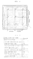
- FIG. 4 shows an embodiment of a prototype produced for measurement.
- each temperature of nine points A to I of the front side (the element formation substrate 1 side) of the organic EL light-emitting device is measured.
- FIG. 5 shows an example of a laminated structure of the prototype of the organic EL element 2.
- the names of layers and the functional materials constituting these layers are shown in FIG. 5 .
- the organic EL element 2 has a multiphoton structure with two light-emitting layers.
- FIG. 6 shows a measured temperature (°C) at the points A to I, shown in FIG. 4 , for a comparison in which nitrogen is filled in the space between the element formation substrate 1 and the sealing substrate 3, a comparison in which a liquid is filled therein, and the case according to this invention in which a gel or a grease is filled therein.
- the measured values are the temperature at a time point after a lapse of 30 minutes from the application of current.
- an aluminum soaking plate with a plate thickness of 0.5 mm, to which a heat dissipating agent such as alumina is applied is attached to the outside of the sealing substrate 3 side through a heat-transfer member.
- the soaking plate other metals such as a copper plate can be used.
- a methylphenyl silicone oil (SH550) from Dow Corning Toray Co., Ltd. reduced in pressure and heated at 100°C is used.
- SH550 methylphenyl silicone oil
- the organic EL light-emitting device according to this invention for example, KE1057 from Shin-Etsu Chemical Co. , Ltd. of 50 wt% as a silicone gel, calcium oxide of 30 wt% as a moisture absorbent, aluminum oxide of 20 wt% as a heat-transfer material are used in the gel layer.
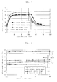
- FIG. 7 shows, in the comparative example in which the liquid is the filler and the organic EL light-emitting device of this invention in which the gel is the filler, the temperature (°C) of the front and back sides of the device at the point E shown in FIG. 4 from the application of current to a lapse of 30 minutes and the subsequent elapse of time after the power off.
- FIG. 8 is an enlarged scale of FIG. 7 and shows the measurement result from the application of current to a lapse of 15 to 30 minutes.
- the measurement result in the organic EL light-emitting device of this invention is expressed as "gel sealed: front (a light extraction side)” and “gel sealed: back (sealing side)".
- the compared measurement result in the prior art example is expressed as "liquid sealed: front (a light extraction side)” and “liquid sealed: back (sealing side)”.
- the organic EL light-emitting device of this invention using the gel as the filler, it can be understood that the average value of the temperatures at points A to I is significantly reduced compared with the light-emitting device using the liquid as the filler. Further, it can be understood that the difference between the maximum value and the minimum value of the points A to I (Max - Min) is extremely small.
- the temperature difference between the front and back sides at the time point after a lapse of 30 minutes from the application of current is about 7.0°C, as represented as Dt1.
- the temperature difference between the front and back sides of the organic EL light-emitting device of this invention at the same time point can be suppressed to about 1. 3°C, as represented as Dt2.
- FIG. 9 schematically shows another embodiment according to the organic EL light-emitting device of this invention.
- components equivalent to those in FIG. 1 are assigned the same reference numerals and detailed explanations thereof are omitted.
- a moisture absorbent layer 6 which is formed of a resin containing a moisture absorbent is further disposed on the surface of the sealing substrate 3 facing the element formation substrate 1.
- the moisture absorbent layer 6 contains the moisture absorbent dispersed in the resin constituting the moisture absorbent layer 6, and catches water by the moisture absorbent to thereby effectively prevent the dark spot from being generated and spread in the organic EL element 2.
- a thermosetting or UV-curable epoxy or acrylic resin can be used, and the moisture absorbent is dispersed in the resin, whereby the moisture absorbent layer 6 is formed.
- the moisture absorbent dispersed in the resin can catch water by chemisorption or physisorption. Specifically, there can be used a similar one to the moisture absorbent contained in the grease layer 5 or the gel layer 5 in a state of being dispersed in the grease layer 5 or the gel layer 5. As shown in FIG. 9 , the moisture absorbent layer 6 is formed so as to be larger than the outer peripheral portion of the light-emitting part L of the organic EL element 2 facing the moisture absorbent layer 6, whereby a satisfactory moisture absorption effect can be exercised.
- An organometallic complex liquid moisture absorbent as the moisture absorbent layer 6 may be applied to be dried or hardened. For example, Ole Dry from Futaba Corporation can be used.
- the moisture absorbent layer 6 is disposed so as to be attached to the sealing substrate 3, whereby the grease layer 5 or the gel layer 5 free from the moisture absorbent can be used in the organic EL light-emitting device.
- the grease layer 5 or the gel layer 5 containing the dispersed moisture absorbent can be used with the moisture absorbent layer 6.
- the grease layer 5 or the gel layer 5 containing the heat-transfer agent dispersed therein and the moisture absorbent layer 6 are provided in the organic EL light-emitting device, whereby the unique heat-transfer properties of the grease layer 5 or the gel layer 5 and the unique heat-transfer properties of the moisture absorbent layer 6 act to contribute to more effective prevention of the occurrence of the brightness unevenness in the organic EL light-emitting device.
- FIG. 10 explains the manufacturing process of the organic EL light-emitting device having the constitution shown in FIG. 9 .
- Themanufacturing process of FIG. 10 is executed by separating the process (A) of FIG. 8A into two processes. Namely, in a process (A1) of FIG. 10 , the moisture absorbent layer 6 is formed on one side of the plate-shaped sealing substrate 3. The grease 5 or the gel agent 5 is then coated onto the surface with the moisture absorbent layer 6 so as to be superimposed on the moisture absorbent layer 6.
- the processes following the process (B) of FIG. 3A are executed, whereby the organic EL light-emitting device with the moisture absorbent layer 6 shown in FIG. 9 can be manufactured. Also in the organic EL light-emitting device having the constitution shown in FIG. 9 , the operational effect described in the effect of the invention can be exercised.
- the plate-shaped sealing substrate 3 is used; however, instead of this, a sealing substrate having a recessed cross-sectional surface in which a recess is provided in the central portion so that the peripheral edge portion is in contact with the element formation substrate, that is, the sealing substrate 3 shown in FIG. 11 can be used.
- FIG. 11 components serving the same function as those in FIG. 1 are assigned the same reference numerals.
- the grease 5 or the gel agent 5 is tightly filled in the recess.
- the sealing substrate and the element formation substrate with the organic EL element may be formed of a flexible resin material.
- each of a pair of the transparent electrode 2A and the opposed electrode 2C constituting the organic EL element 2 is formed in a planar shape (as a solid electrode) so as to follow the surface of the element formation substrate 1.
- the transparent electrode 2A is formed in a stripe shape
- the opposed electrode 2C is formed in a stripe shape so as to be perpendicular to the transparent electrode 2A, whereby the organic EL element is divided at the intersection between these electrodes, and thus the organic EL element with a plurality of light-emitting parts can be obtained.
- This invention can be applied to an organic light-emitting device in which a plurality of the light-emitting parts of the organic EL element are arranged, as described above, and a similar operational effect can be obtained. In this case, even in an organic light-emitting device with a plurality of series-connected organic EL elements (surface series structure), a similar operational effect can be obtained.
Landscapes
- Physics & Mathematics (AREA)
- Optics & Photonics (AREA)
- Engineering & Computer Science (AREA)
- Manufacturing & Machinery (AREA)
- Electroluminescent Light Sources (AREA)
- Compositions Of Macromolecular Compounds (AREA)
Applications Claiming Priority (2)
| Application Number | Priority Date | Filing Date | Title |
|---|---|---|---|
| JP2008124330 | 2008-05-12 | ||
| PCT/JP2009/058340 WO2009139292A1 (fr) | 2008-05-12 | 2009-04-28 | Dispositif électroluminescent (el) organique et procédé de production associé |
Publications (3)
| Publication Number | Publication Date |
|---|---|
| EP2285183A1 true EP2285183A1 (fr) | 2011-02-16 |
| EP2285183A4 EP2285183A4 (fr) | 2013-12-25 |
| EP2285183B1 EP2285183B1 (fr) | 2019-08-28 |
Family
ID=41318663
Family Applications (1)
| Application Number | Title | Priority Date | Filing Date |
|---|---|---|---|
| EP09746499.4A Active EP2285183B1 (fr) | 2008-05-12 | 2009-04-28 | Procédé de fabrication d'un dispositif électroluminescent organique |
Country Status (5)
| Country | Link |
|---|---|
| US (1) | US8563112B2 (fr) |
| EP (1) | EP2285183B1 (fr) |
| JP (1) | JPWO2009139292A1 (fr) |
| TW (1) | TWI526114B (fr) |
| WO (1) | WO2009139292A1 (fr) |
Cited By (2)
| Publication number | Priority date | Publication date | Assignee | Title |
|---|---|---|---|---|
| EP3439432A4 (fr) * | 2016-03-31 | 2020-01-15 | Lumiotec Inc. | Panneau électroluminescent organique et son procédé de fabrication |
| EP3488478B1 (fr) * | 2016-07-19 | 2023-04-19 | BOE Technology Group Co., Ltd. | Procédé de fabrication de panneau d'affichage |
Families Citing this family (24)
| Publication number | Priority date | Publication date | Assignee | Title |
|---|---|---|---|---|
| JP5111201B2 (ja) | 2008-03-31 | 2013-01-09 | 株式会社ジャパンディスプレイイースト | 有機el表示装置 |
| JP5407819B2 (ja) * | 2009-12-07 | 2014-02-05 | 凸版印刷株式会社 | 有機エレクトロルミネッセンスディスプレイ及びその製造方法 |
| JP5731830B2 (ja) * | 2010-01-19 | 2015-06-10 | パナソニック株式会社 | 面状発光装置 |
| ITMI20100080U1 (it) * | 2010-03-22 | 2011-09-23 | Getters Spa | Composizione per la protezione di dispositivi sensibili alla presenza di h2o. |
| KR101193198B1 (ko) | 2010-07-12 | 2012-10-26 | 삼성디스플레이 주식회사 | 유기 발광 장치 및 이의 제조 방법 |
| JP5842088B2 (ja) * | 2011-02-21 | 2016-01-13 | パナソニックIpマネジメント株式会社 | 有機elデバイス及び有機elデバイスの製造方法 |
| CN103085437B (zh) * | 2011-11-02 | 2016-04-06 | 宸鸿科技(厦门)有限公司 | 贴合结构、具有该贴合结构之电子装置及其贴合方法 |
| KR101469267B1 (ko) * | 2011-12-28 | 2014-12-08 | 제일모직주식회사 | 게터 조성물 및 이를 포함하는 유기 el 디스플레이 장치 |
| JP6083989B2 (ja) * | 2012-09-24 | 2017-02-22 | パイオニア株式会社 | 吸湿性成形体 |
| TWI587502B (zh) * | 2012-10-31 | 2017-06-11 | 財團法人工業技術研究院 | 環境敏感電子元件封裝體 |
| US9565793B2 (en) | 2012-10-31 | 2017-02-07 | Industrial Technology Research Institute | Environmental sensitive electronic device package |
| KR102103421B1 (ko) | 2013-02-07 | 2020-04-23 | 삼성디스플레이 주식회사 | 유기 발광 표시 장치 및 그 제조 방법 |
| CN105493627A (zh) | 2013-08-28 | 2016-04-13 | 夏普株式会社 | 电致发光装置及其制造方法 |
| JP6040140B2 (ja) * | 2013-12-06 | 2016-12-07 | 双葉電子工業株式会社 | 有機エレクトロルミネッセンスデバイス |
| KR20160093560A (ko) * | 2015-01-29 | 2016-08-08 | 모멘티브퍼포먼스머티리얼스코리아 주식회사 | 유기 전자 소자 봉지재용 조성물 및 이를 이용하여 형성된 봉지재 |
| JP6854240B2 (ja) | 2015-08-18 | 2021-04-07 | 株式会社ホタルクス | 有機elデバイス、有機el照明パネル、有機el照明装置および有機elディスプレイ |
| JP6654505B2 (ja) * | 2016-05-18 | 2020-02-26 | 双葉電子工業株式会社 | 乾燥剤、封止構造、及び有機el素子 |
| CN107785501B (zh) | 2017-10-17 | 2019-12-24 | 深圳市华星光电半导体显示技术有限公司 | 柔性oled面板的封装方法及封装结构 |
| TWI762711B (zh) * | 2017-11-07 | 2022-05-01 | 日商双葉電子工業股份有限公司 | 乾燥劑、密封結構體及有機電致發光元件 |
| US10497838B2 (en) * | 2018-04-12 | 2019-12-03 | Osram Opto Semiconductors Gmbh | Method for producing an optic device, optic device and assembly comprising such an optic device |
| JP6973360B2 (ja) * | 2018-11-26 | 2021-11-24 | 信越化学工業株式会社 | 吸湿性シリコーン樹脂組成物、有機el用透明封止材、有機el用透明乾燥材、及びその使用方法 |
| US11264279B2 (en) * | 2019-04-16 | 2022-03-01 | Next Biometrics Group Asa | Systems and methods for manufacturing flexible electronics |
| JP2021170450A (ja) * | 2020-04-15 | 2021-10-28 | 双葉電子工業株式会社 | 乾燥剤、封止構造体、及び有機el素子 |
| JP2022160191A (ja) * | 2021-04-06 | 2022-10-19 | 双葉電子工業株式会社 | 乾燥剤組成物、封止構造体、有機elデバイス、及び、有機elデバイスを製造する方法 |
Family Cites Families (33)
| Publication number | Priority date | Publication date | Assignee | Title |
|---|---|---|---|---|
| US5276414A (en) * | 1991-12-10 | 1994-01-04 | Mitsubishi Denki Kabushiki Kaisha | Moistureproof structure for module circuits |
| EP0567085A2 (fr) * | 1992-04-22 | 1993-10-27 | Matsushita Electric Industrial Co., Ltd. | Méthode d'enregistrement à transfert thermique |
| JPH09204981A (ja) * | 1996-01-26 | 1997-08-05 | Nippon Steel Chem Co Ltd | 有機el素子 |
| JPH09330788A (ja) * | 1996-06-06 | 1997-12-22 | Casio Comput Co Ltd | 電界発光素子 |
| US5734225A (en) * | 1996-07-10 | 1998-03-31 | International Business Machines Corporation | Encapsulation of organic light emitting devices using siloxane or siloxane derivatives |
| JPH1074583A (ja) * | 1996-08-30 | 1998-03-17 | Sanyo Electric Co Ltd | 有機elディスプレイ及び有機elディスプレイの 製造方法 |
| US5895228A (en) * | 1996-11-14 | 1999-04-20 | International Business Machines Corporation | Encapsulation of organic light emitting devices using Siloxane or Siloxane derivatives |
| JP3411864B2 (ja) | 1999-06-11 | 2003-06-03 | ティーディーケイ株式会社 | 有機el表示装置 |
| JP2001026073A (ja) * | 1999-07-13 | 2001-01-30 | Inoac Corp | 防水封止材 |
| JP2001068266A (ja) * | 1999-08-24 | 2001-03-16 | Toyota Motor Corp | 有機el素子及びその製造方法 |
| JP3702134B2 (ja) * | 1999-11-18 | 2005-10-05 | 株式会社巴川製紙所 | 光学接続部品の作製方法 |
| JP2001217071A (ja) | 2000-02-02 | 2001-08-10 | Nippon Seiki Co Ltd | 有機el素子の製造方法 |
| JP2001282120A (ja) | 2000-03-31 | 2001-10-12 | Minolta Co Ltd | 表示パネルの製造方法及び装置 |
| US6739929B2 (en) | 2000-03-31 | 2004-05-25 | Minolta Co., Ltd. | Method and apparatus for producing a display panel, method for adhering an adhesive sheet and method for adhering plates |
| WO2001084194A1 (fr) * | 2000-04-27 | 2001-11-08 | Tomoegawa Paper Co., Ltd. | Composant de connexion optique |
| JP2002333848A (ja) | 2001-05-10 | 2002-11-22 | Sharp Corp | 複合アクティブマトリクス基板、その製造方法、及び電磁波撮像装置 |
| JP2003007450A (ja) * | 2001-06-20 | 2003-01-10 | Matsushita Electric Ind Co Ltd | 発光素子、表示装置及び照明装置 |
| JP2003173868A (ja) | 2001-09-28 | 2003-06-20 | Sanyo Electric Co Ltd | エレクトロルミネッセンスパネルの製造方法 |
| US7453705B2 (en) * | 2002-05-07 | 2008-11-18 | Alien Technology Corporation | Barrier, such as a hermetic barrier layer for O/PLED and other electronic devices on plastic |
| JP2004265776A (ja) * | 2003-03-03 | 2004-09-24 | Hitachi Ltd | 有機elディスプレイ装置 |
| JP3962927B2 (ja) * | 2003-05-01 | 2007-08-22 | 信越化学工業株式会社 | 電気電子部品を保護する封止材の除去方法 |
| EP1494296A1 (fr) * | 2003-07-04 | 2005-01-05 | CFG S.A.Microelectronic | Dispositif électroluminescent |
| US7792489B2 (en) | 2003-12-26 | 2010-09-07 | Semiconductor Energy Laboratory Co., Ltd. | Light emitting device, electronic appliance, and method for manufacturing light emitting device |
| JP4801346B2 (ja) * | 2003-12-26 | 2011-10-26 | 株式会社半導体エネルギー研究所 | 発光装置の作製方法 |
| US7316756B2 (en) * | 2004-07-27 | 2008-01-08 | Eastman Kodak Company | Desiccant for top-emitting OLED |
| JP2006128022A (ja) * | 2004-11-01 | 2006-05-18 | Seiko Epson Corp | 発光装置、発光装置の製造方法、及び電子機器 |
| JP2006179218A (ja) * | 2004-12-21 | 2006-07-06 | Asahi Glass Co Ltd | 有機elパネル及び有機el発光装置、並びに有機elパネルの製造方法 |
| JP2006221901A (ja) * | 2005-02-09 | 2006-08-24 | Seiko Epson Corp | 発光装置、ラインヘッド、発光装置の製造方法、ラインヘッドの製造方法、電子機器、及び画像形成装置 |
| JP4544424B2 (ja) * | 2005-06-06 | 2010-09-15 | 信越化学工業株式会社 | 電気電子部品保護用封止材の除去方法 |
| JP2007300069A (ja) * | 2006-04-04 | 2007-11-15 | Toyoda Gosei Co Ltd | 発光素子、この発光素子を用いた発光装置及びこの発光素子の製造方法 |
| JP2008077943A (ja) | 2006-09-20 | 2008-04-03 | Fuji Electric Holdings Co Ltd | 多色発光デバイス |
| JP2008085172A (ja) * | 2006-09-28 | 2008-04-10 | Shinetsu Astec Kk | 発光装置 |
| CN101196966B (zh) * | 2006-12-08 | 2010-05-19 | 华为技术有限公司 | 许可证交互及其中断后恢复的方法及数字版权管理系统 |
-
2009
- 2009-04-28 WO PCT/JP2009/058340 patent/WO2009139292A1/fr not_active Ceased
- 2009-04-28 EP EP09746499.4A patent/EP2285183B1/fr active Active
- 2009-04-28 JP JP2010511947A patent/JPWO2009139292A1/ja active Pending
- 2009-04-28 US US12/990,901 patent/US8563112B2/en not_active Expired - Fee Related
- 2009-05-06 TW TW098114972A patent/TWI526114B/zh not_active IP Right Cessation
Cited By (2)
| Publication number | Priority date | Publication date | Assignee | Title |
|---|---|---|---|---|
| EP3439432A4 (fr) * | 2016-03-31 | 2020-01-15 | Lumiotec Inc. | Panneau électroluminescent organique et son procédé de fabrication |
| EP3488478B1 (fr) * | 2016-07-19 | 2023-04-19 | BOE Technology Group Co., Ltd. | Procédé de fabrication de panneau d'affichage |
Also Published As
| Publication number | Publication date |
|---|---|
| TWI526114B (zh) | 2016-03-11 |
| TW200948180A (en) | 2009-11-16 |
| US20110052857A1 (en) | 2011-03-03 |
| EP2285183B1 (fr) | 2019-08-28 |
| EP2285183A4 (fr) | 2013-12-25 |
| WO2009139292A1 (fr) | 2009-11-19 |
| US8563112B2 (en) | 2013-10-22 |
| JPWO2009139292A1 (ja) | 2011-09-22 |
Similar Documents
| Publication | Publication Date | Title |
|---|---|---|
| EP2285183B1 (fr) | Procédé de fabrication d'un dispositif électroluminescent organique | |
| US20110045732A1 (en) | Method and device for manufacturing organic el light-emitting panel | |
| US20030066311A1 (en) | Encapsulation of a display element and method of forming the same | |
| KR101160736B1 (ko) | 면발광체 | |
| US7205718B2 (en) | OLED display having thermally conductive adhesive | |
| JP6070558B2 (ja) | 有機エレクトロルミネッセンス発光装置及びその製造方法 | |
| CN1200465C (zh) | 显示元件的封装结构及其形成方法 | |
| JP4861206B2 (ja) | 有機エレクトロルミネッセンス発光装置及び有機エレクトロルミネッセンス照明装置 | |
| TWI236862B (en) | Package for OLED device | |
| US20100258839A1 (en) | Organic electroluminescence device and method for manufacturing the same | |
| US9660222B2 (en) | Light-emitting device and method for manufacturing the same | |
| JP2011048937A (ja) | 有機el発光素子 | |
| JP6751459B2 (ja) | 有機エレクトロルミネッセンス照明パネル、その製造方法及び有機エレクトロルミネッセンス照明装置 | |
| JP5319420B2 (ja) | 有機エレクトロルミネッセンス素子 | |
| CN102308409B (zh) | 电致发光装置 | |
| JP5144041B2 (ja) | 有機エレクトロルミネッセンス発光装置及び有機エレクトロルミネッセンス照明装置 | |
| JP6160107B2 (ja) | 有機エレクトロルミネッセンス発光装置、有機el表示装置及び有機el照明 | |
| CN102308411A (zh) | 电致发光装置 | |
| JP2006331695A (ja) | 有機発光素子用封止部材及び有機発光素子 | |
| JP2012199207A (ja) | 有機エレクトロルミネッセンスディスプレイ及びその製造方法 | |
| CN108428804A (zh) | Oled显示面板及其封装方法 | |
| JP5106467B2 (ja) | 有機el装置 | |
| US10084158B2 (en) | Optoelectronic component and method of producing an optoelectronic component | |
| KR102662113B1 (ko) | 언더필소재가 충진되는 단차공간을 포함하는 led방열기판 | |
| JP4852590B2 (ja) | 有機エレクトロルミネッセンス素子 |
Legal Events
| Date | Code | Title | Description |
|---|---|---|---|
| PUAI | Public reference made under article 153(3) epc to a published international application that has entered the european phase |
Free format text: ORIGINAL CODE: 0009012 |
|
| 17P | Request for examination filed |
Effective date: 20101111 |
|
| AK | Designated contracting states |
Kind code of ref document: A1 Designated state(s): AT BE BG CH CY CZ DE DK EE ES FI FR GB GR HR HU IE IS IT LI LT LU LV MC MK MT NL NO PL PT RO SE SI SK TR |
|
| AX | Request for extension of the european patent |
Extension state: AL BA RS |
|
| DAX | Request for extension of the european patent (deleted) | ||
| A4 | Supplementary search report drawn up and despatched |
Effective date: 20131126 |
|
| RIC1 | Information provided on ipc code assigned before grant |
Ipc: H05B 33/10 20060101ALI20131120BHEP Ipc: H05B 33/04 20060101AFI20131120BHEP Ipc: H01L 51/52 20060101ALI20131120BHEP Ipc: H01L 51/50 20060101ALI20131120BHEP |
|
| STAA | Information on the status of an ep patent application or granted ep patent |
Free format text: STATUS: EXAMINATION IS IN PROGRESS |
|
| 17Q | First examination report despatched |
Effective date: 20180419 |
|
| GRAP | Despatch of communication of intention to grant a patent |
Free format text: ORIGINAL CODE: EPIDOSNIGR1 |
|
| STAA | Information on the status of an ep patent application or granted ep patent |
Free format text: STATUS: GRANT OF PATENT IS INTENDED |
|
| INTG | Intention to grant announced |
Effective date: 20190405 |
|
| GRAS | Grant fee paid |
Free format text: ORIGINAL CODE: EPIDOSNIGR3 |
|
| GRAA | (expected) grant |
Free format text: ORIGINAL CODE: 0009210 |
|
| STAA | Information on the status of an ep patent application or granted ep patent |
Free format text: STATUS: THE PATENT HAS BEEN GRANTED |
|
| AK | Designated contracting states |
Kind code of ref document: B1 Designated state(s): AT BE BG CH CY CZ DE DK EE ES FI FR GB GR HR HU IE IS IT LI LT LU LV MC MK MT NL NO PL PT RO SE SI SK TR |
|
| REG | Reference to a national code |
Ref country code: GB Ref legal event code: FG4D |
|
| REG | Reference to a national code |
Ref country code: CH Ref legal event code: EP |
|
| REG | Reference to a national code |
Ref country code: AT Ref legal event code: REF Ref document number: 1174041 Country of ref document: AT Kind code of ref document: T Effective date: 20190915 |
|
| REG | Reference to a national code |
Ref country code: IE Ref legal event code: FG4D |
|
| REG | Reference to a national code |
Ref country code: DE Ref legal event code: R096 Ref document number: 602009059619 Country of ref document: DE |
|
| REG | Reference to a national code |
Ref country code: NL Ref legal event code: FP |
|
| REG | Reference to a national code |
Ref country code: LT Ref legal event code: MG4D |
|
| REG | Reference to a national code |
Ref country code: NL Ref legal event code: PD Owner name: HOTALUX, LTD.; JP Free format text: DETAILS ASSIGNMENT: CHANGE OF OWNER(S), DEMERGER; FORMER OWNER NAME: YAMAGATA PROMOTIONAL ORGANIZATION FOR INDUSTRIAL TECHNOLOGY Effective date: 20200108 |
|
| PG25 | Lapsed in a contracting state [announced via postgrant information from national office to epo] |
Ref country code: SE Free format text: LAPSE BECAUSE OF FAILURE TO SUBMIT A TRANSLATION OF THE DESCRIPTION OR TO PAY THE FEE WITHIN THE PRESCRIBED TIME-LIMIT Effective date: 20190828 Ref country code: BG Free format text: LAPSE BECAUSE OF FAILURE TO SUBMIT A TRANSLATION OF THE DESCRIPTION OR TO PAY THE FEE WITHIN THE PRESCRIBED TIME-LIMIT Effective date: 20191128 Ref country code: NO Free format text: LAPSE BECAUSE OF FAILURE TO SUBMIT A TRANSLATION OF THE DESCRIPTION OR TO PAY THE FEE WITHIN THE PRESCRIBED TIME-LIMIT Effective date: 20191128 Ref country code: LT Free format text: LAPSE BECAUSE OF FAILURE TO SUBMIT A TRANSLATION OF THE DESCRIPTION OR TO PAY THE FEE WITHIN THE PRESCRIBED TIME-LIMIT Effective date: 20190828 Ref country code: HR Free format text: LAPSE BECAUSE OF FAILURE TO SUBMIT A TRANSLATION OF THE DESCRIPTION OR TO PAY THE FEE WITHIN THE PRESCRIBED TIME-LIMIT Effective date: 20190828 Ref country code: FI Free format text: LAPSE BECAUSE OF FAILURE TO SUBMIT A TRANSLATION OF THE DESCRIPTION OR TO PAY THE FEE WITHIN THE PRESCRIBED TIME-LIMIT Effective date: 20190828 Ref country code: PT Free format text: LAPSE BECAUSE OF FAILURE TO SUBMIT A TRANSLATION OF THE DESCRIPTION OR TO PAY THE FEE WITHIN THE PRESCRIBED TIME-LIMIT Effective date: 20191230 |
|
| REG | Reference to a national code |
Ref country code: DE Ref legal event code: R082 Ref document number: 602009059619 Country of ref document: DE Representative=s name: HOFFMANN - EITLE PATENT- UND RECHTSANWAELTE PA, DE Ref country code: DE Ref legal event code: R081 Ref document number: 602009059619 Country of ref document: DE Owner name: HOTALUX, LTD., JP Free format text: FORMER OWNERS: NEC LIGHTING, LTD., TOKYO, JP; YAMAGATA PROMOTIONAL ORGANIZATION FOR INDUSTRIAL TECHNOLOGY, YAMAGATA, JP Ref country code: DE Ref legal event code: R081 Ref document number: 602009059619 Country of ref document: DE Owner name: YAMAGATA PROMOTIONAL ORGANIZATION FOR INDUSTRI, JP Free format text: FORMER OWNERS: NEC LIGHTING, LTD., TOKYO, JP; YAMAGATA PROMOTIONAL ORGANIZATION FOR INDUSTRIAL TECHNOLOGY, YAMAGATA, JP |
|
| PG25 | Lapsed in a contracting state [announced via postgrant information from national office to epo] |
Ref country code: GR Free format text: LAPSE BECAUSE OF FAILURE TO SUBMIT A TRANSLATION OF THE DESCRIPTION OR TO PAY THE FEE WITHIN THE PRESCRIBED TIME-LIMIT Effective date: 20191129 Ref country code: ES Free format text: LAPSE BECAUSE OF FAILURE TO SUBMIT A TRANSLATION OF THE DESCRIPTION OR TO PAY THE FEE WITHIN THE PRESCRIBED TIME-LIMIT Effective date: 20190828 Ref country code: LV Free format text: LAPSE BECAUSE OF FAILURE TO SUBMIT A TRANSLATION OF THE DESCRIPTION OR TO PAY THE FEE WITHIN THE PRESCRIBED TIME-LIMIT Effective date: 20190828 Ref country code: IS Free format text: LAPSE BECAUSE OF FAILURE TO SUBMIT A TRANSLATION OF THE DESCRIPTION OR TO PAY THE FEE WITHIN THE PRESCRIBED TIME-LIMIT Effective date: 20191228 |
|
| REG | Reference to a national code |
Ref country code: AT Ref legal event code: MK05 Ref document number: 1174041 Country of ref document: AT Kind code of ref document: T Effective date: 20190828 |
|
| PG25 | Lapsed in a contracting state [announced via postgrant information from national office to epo] |
Ref country code: TR Free format text: LAPSE BECAUSE OF FAILURE TO SUBMIT A TRANSLATION OF THE DESCRIPTION OR TO PAY THE FEE WITHIN THE PRESCRIBED TIME-LIMIT Effective date: 20190828 |
|
| PG25 | Lapsed in a contracting state [announced via postgrant information from national office to epo] |
Ref country code: AT Free format text: LAPSE BECAUSE OF FAILURE TO SUBMIT A TRANSLATION OF THE DESCRIPTION OR TO PAY THE FEE WITHIN THE PRESCRIBED TIME-LIMIT Effective date: 20190828 Ref country code: RO Free format text: LAPSE BECAUSE OF FAILURE TO SUBMIT A TRANSLATION OF THE DESCRIPTION OR TO PAY THE FEE WITHIN THE PRESCRIBED TIME-LIMIT Effective date: 20190828 Ref country code: PL Free format text: LAPSE BECAUSE OF FAILURE TO SUBMIT A TRANSLATION OF THE DESCRIPTION OR TO PAY THE FEE WITHIN THE PRESCRIBED TIME-LIMIT Effective date: 20190828 Ref country code: EE Free format text: LAPSE BECAUSE OF FAILURE TO SUBMIT A TRANSLATION OF THE DESCRIPTION OR TO PAY THE FEE WITHIN THE PRESCRIBED TIME-LIMIT Effective date: 20190828 Ref country code: IT Free format text: LAPSE BECAUSE OF FAILURE TO SUBMIT A TRANSLATION OF THE DESCRIPTION OR TO PAY THE FEE WITHIN THE PRESCRIBED TIME-LIMIT Effective date: 20190828 Ref country code: DK Free format text: LAPSE BECAUSE OF FAILURE TO SUBMIT A TRANSLATION OF THE DESCRIPTION OR TO PAY THE FEE WITHIN THE PRESCRIBED TIME-LIMIT Effective date: 20190828 |
|
| PG25 | Lapsed in a contracting state [announced via postgrant information from national office to epo] |
Ref country code: IS Free format text: LAPSE BECAUSE OF FAILURE TO SUBMIT A TRANSLATION OF THE DESCRIPTION OR TO PAY THE FEE WITHIN THE PRESCRIBED TIME-LIMIT Effective date: 20200224 Ref country code: CZ Free format text: LAPSE BECAUSE OF FAILURE TO SUBMIT A TRANSLATION OF THE DESCRIPTION OR TO PAY THE FEE WITHIN THE PRESCRIBED TIME-LIMIT Effective date: 20190828 Ref country code: SK Free format text: LAPSE BECAUSE OF FAILURE TO SUBMIT A TRANSLATION OF THE DESCRIPTION OR TO PAY THE FEE WITHIN THE PRESCRIBED TIME-LIMIT Effective date: 20190828 |
|
| REG | Reference to a national code |
Ref country code: DE Ref legal event code: R097 Ref document number: 602009059619 Country of ref document: DE |
|
| PLBE | No opposition filed within time limit |
Free format text: ORIGINAL CODE: 0009261 |
|
| STAA | Information on the status of an ep patent application or granted ep patent |
Free format text: STATUS: NO OPPOSITION FILED WITHIN TIME LIMIT |
|
| PG2D | Information on lapse in contracting state deleted |
Ref country code: IS |
|
| 26N | No opposition filed |
Effective date: 20200603 |
|
| PG25 | Lapsed in a contracting state [announced via postgrant information from national office to epo] |
Ref country code: SI Free format text: LAPSE BECAUSE OF FAILURE TO SUBMIT A TRANSLATION OF THE DESCRIPTION OR TO PAY THE FEE WITHIN THE PRESCRIBED TIME-LIMIT Effective date: 20190828 |
|
| REG | Reference to a national code |
Ref country code: DE Ref legal event code: R119 Ref document number: 602009059619 Country of ref document: DE |
|
| PG25 | Lapsed in a contracting state [announced via postgrant information from national office to epo] |
Ref country code: MC Free format text: LAPSE BECAUSE OF FAILURE TO SUBMIT A TRANSLATION OF THE DESCRIPTION OR TO PAY THE FEE WITHIN THE PRESCRIBED TIME-LIMIT Effective date: 20190828 |
|
| REG | Reference to a national code |
Ref country code: CH Ref legal event code: PL |
|
| REG | Reference to a national code |
Ref country code: NL Ref legal event code: MM Effective date: 20200501 |
|
| PG25 | Lapsed in a contracting state [announced via postgrant information from national office to epo] |
Ref country code: CH Free format text: LAPSE BECAUSE OF NON-PAYMENT OF DUE FEES Effective date: 20200430 Ref country code: LU Free format text: LAPSE BECAUSE OF NON-PAYMENT OF DUE FEES Effective date: 20200428 Ref country code: FR Free format text: LAPSE BECAUSE OF NON-PAYMENT OF DUE FEES Effective date: 20200430 Ref country code: LI Free format text: LAPSE BECAUSE OF NON-PAYMENT OF DUE FEES Effective date: 20200430 Ref country code: DE Free format text: LAPSE BECAUSE OF NON-PAYMENT OF DUE FEES Effective date: 20201103 |
|
| REG | Reference to a national code |
Ref country code: BE Ref legal event code: MM Effective date: 20200430 |
|
| PG25 | Lapsed in a contracting state [announced via postgrant information from national office to epo] |
Ref country code: BE Free format text: LAPSE BECAUSE OF NON-PAYMENT OF DUE FEES Effective date: 20200430 |
|
| GBPC | Gb: european patent ceased through non-payment of renewal fee |
Effective date: 20200428 |
|
| PG25 | Lapsed in a contracting state [announced via postgrant information from national office to epo] |
Ref country code: NL Free format text: LAPSE BECAUSE OF NON-PAYMENT OF DUE FEES Effective date: 20200501 |
|
| PG25 | Lapsed in a contracting state [announced via postgrant information from national office to epo] |
Ref country code: GB Free format text: LAPSE BECAUSE OF NON-PAYMENT OF DUE FEES Effective date: 20200428 Ref country code: IE Free format text: LAPSE BECAUSE OF NON-PAYMENT OF DUE FEES Effective date: 20200428 |
|
| PG25 | Lapsed in a contracting state [announced via postgrant information from national office to epo] |
Ref country code: MT Free format text: LAPSE BECAUSE OF FAILURE TO SUBMIT A TRANSLATION OF THE DESCRIPTION OR TO PAY THE FEE WITHIN THE PRESCRIBED TIME-LIMIT Effective date: 20190828 Ref country code: CY Free format text: LAPSE BECAUSE OF FAILURE TO SUBMIT A TRANSLATION OF THE DESCRIPTION OR TO PAY THE FEE WITHIN THE PRESCRIBED TIME-LIMIT Effective date: 20190828 |
|
| PG25 | Lapsed in a contracting state [announced via postgrant information from national office to epo] |
Ref country code: MK Free format text: LAPSE BECAUSE OF FAILURE TO SUBMIT A TRANSLATION OF THE DESCRIPTION OR TO PAY THE FEE WITHIN THE PRESCRIBED TIME-LIMIT Effective date: 20190828 |