EP2287901A2 - Améliorations associées aux dispositifs semi-conducteurs - Google Patents
Améliorations associées aux dispositifs semi-conducteurs Download PDFInfo
- Publication number
- EP2287901A2 EP2287901A2 EP10186092A EP10186092A EP2287901A2 EP 2287901 A2 EP2287901 A2 EP 2287901A2 EP 10186092 A EP10186092 A EP 10186092A EP 10186092 A EP10186092 A EP 10186092A EP 2287901 A2 EP2287901 A2 EP 2287901A2
- Authority
- EP
- European Patent Office
- Prior art keywords
- layer
- oxide
- trenches
- depositing
- trench
- Prior art date
- Legal status (The legal status is an assumption and is not a legal conclusion. Google has not performed a legal analysis and makes no representation as to the accuracy of the status listed.)
- Ceased
Links
Images


Classifications
-
- H—ELECTRICITY
- H10—SEMICONDUCTOR DEVICES; ELECTRIC SOLID-STATE DEVICES NOT OTHERWISE PROVIDED FOR
- H10P—GENERIC PROCESSES OR APPARATUS FOR THE MANUFACTURE OR TREATMENT OF DEVICES COVERED BY CLASS H10
- H10P14/00—Formation of materials, e.g. in the shape of layers or pillars
- H10P14/60—Formation of materials, e.g. in the shape of layers or pillars of insulating materials
- H10P14/63—Formation of materials, e.g. in the shape of layers or pillars of insulating materials characterised by the formation processes
- H10P14/6326—Deposition processes
- H10P14/6328—Deposition from the gas or vapour phase
- H10P14/6334—Deposition from the gas or vapour phase using decomposition or reaction of gaseous or vapour phase compounds, i.e. chemical vapour deposition
- H10P14/6336—Deposition from the gas or vapour phase using decomposition or reaction of gaseous or vapour phase compounds, i.e. chemical vapour deposition in the presence of a plasma [PECVD]
-
- H—ELECTRICITY
- H10—SEMICONDUCTOR DEVICES; ELECTRIC SOLID-STATE DEVICES NOT OTHERWISE PROVIDED FOR
- H10P—GENERIC PROCESSES OR APPARATUS FOR THE MANUFACTURE OR TREATMENT OF DEVICES COVERED BY CLASS H10
- H10P14/00—Formation of materials, e.g. in the shape of layers or pillars
- H10P14/60—Formation of materials, e.g. in the shape of layers or pillars of insulating materials
- H10P14/69—Inorganic materials
- H10P14/692—Inorganic materials composed of oxides, glassy oxides or oxide-based glasses
- H10P14/6921—Inorganic materials composed of oxides, glassy oxides or oxide-based glasses containing silicon
- H10P14/69215—Inorganic materials composed of oxides, glassy oxides or oxide-based glasses containing silicon the material being a silicon oxide, e.g. SiO2
-
- H—ELECTRICITY
- H10—SEMICONDUCTOR DEVICES; ELECTRIC SOLID-STATE DEVICES NOT OTHERWISE PROVIDED FOR
- H10P—GENERIC PROCESSES OR APPARATUS FOR THE MANUFACTURE OR TREATMENT OF DEVICES COVERED BY CLASS H10
- H10P95/00—Generic processes or apparatus for manufacture or treatments not covered by the other groups of this subclass
- H10P95/06—Planarisation of inorganic insulating materials
- H10P95/062—Planarisation of inorganic insulating materials involving a dielectric removal step
- H10P95/064—Planarisation of inorganic insulating materials involving a dielectric removal step the removal being chemical etching
-
- H—ELECTRICITY
- H10—SEMICONDUCTOR DEVICES; ELECTRIC SOLID-STATE DEVICES NOT OTHERWISE PROVIDED FOR
- H10W—GENERIC PACKAGES, INTERCONNECTIONS, CONNECTORS OR OTHER CONSTRUCTIONAL DETAILS OF DEVICES COVERED BY CLASS H10
- H10W10/00—Isolation regions in semiconductor bodies between components of integrated devices
- H10W10/01—Manufacture or treatment
- H10W10/011—Manufacture or treatment of isolation regions comprising dielectric materials
- H10W10/014—Manufacture or treatment of isolation regions comprising dielectric materials using trench refilling with dielectric materials, e.g. shallow trench isolations
- H10W10/0143—Manufacture or treatment of isolation regions comprising dielectric materials using trench refilling with dielectric materials, e.g. shallow trench isolations comprising concurrently refilling multiple trenches having different shapes or dimensions
-
- H—ELECTRICITY
- H10—SEMICONDUCTOR DEVICES; ELECTRIC SOLID-STATE DEVICES NOT OTHERWISE PROVIDED FOR
- H10W—GENERIC PACKAGES, INTERCONNECTIONS, CONNECTORS OR OTHER CONSTRUCTIONAL DETAILS OF DEVICES COVERED BY CLASS H10
- H10W10/00—Isolation regions in semiconductor bodies between components of integrated devices
- H10W10/10—Isolation regions comprising dielectric materials
- H10W10/17—Isolation regions comprising dielectric materials formed using trench refilling with dielectric materials, e.g. shallow trench isolations
-
- Y—GENERAL TAGGING OF NEW TECHNOLOGICAL DEVELOPMENTS; GENERAL TAGGING OF CROSS-SECTIONAL TECHNOLOGIES SPANNING OVER SEVERAL SECTIONS OF THE IPC; TECHNICAL SUBJECTS COVERED BY FORMER USPC CROSS-REFERENCE ART COLLECTIONS [XRACs] AND DIGESTS
- Y10—TECHNICAL SUBJECTS COVERED BY FORMER USPC
- Y10S—TECHNICAL SUBJECTS COVERED BY FORMER USPC CROSS-REFERENCE ART COLLECTIONS [XRACs] AND DIGESTS
- Y10S148/00—Metal treatment
- Y10S148/05—Etch and refill
Definitions
- the present invention relates to semiconductor devices, and more particularly to integrated circuit insulation and methods of fabrication.
- Integrated circuits typically include field effect transistors with source/drains formed in a silicon substrate and with insulated gates on the substrate plus multiple overlying metal (or polysilicon) wiring levels with an insulating layer between the gates/sources/drains and the first metal level wiring and between successive metal level wirings.
- Vertical vias in the insulating layers filled with metal (or polysilicon) provide connections between adjacent metal level wirings and between the gate/source/drain and the first metal level wiring.
- the transistors are isolated from one another on the substrate by insulation areas formed by oxidation. This local oxidation of the silicon (LOGOS) substrate for device isolation has problems including the "bird's beak" lateral encroachment into device areas by the isolating oxide during its growth. This lateral encroachment occupies intolerably large fractions of the available silicon substrate area as the transistor size decreases.
- the deposition uses a gas mixture of silane (SiH4) and nitrous oxide (N 2 O) and begins with the silane to nitrous oxide ratio set to deposit oxide faster than it is sputtered off for surfaces tilted less than 30 or more than 60 degrees from the direction of ion bombardment from the plasma. Once the trenches are filled (and large areas between the trenches have accumulated thick oxide deposits), then the silane to nitrous oxide ratio is adjusted to deposit oxide faster than it is sputtered off for surfaces tilted about 0 or more than 80 degrees from the direction of ion bombardment. This second step of plasma deposition basically contracts the oxide deposits on the areas between the trenches.
- SiH4 silane
- N 2 O nitrous oxide
- Alternative trench isolation schemes include filling the trenches with spin on glasses such as hydrogen silsesquioxane (HSQ) or chemical vapor deposition using ozone plus tetrathoxysilane (TEOS).
- spin on glasses such as hydrogen silsesquioxane (HSQ) or chemical vapor deposition using ozone plus tetrathoxysilane (TEOS).
- the present invention provides a trench isolation scheme using an inductively coupled high density plasma enhanced deposition of oxide for trench filling along with chemical mechanical polishing of the deposited oxide using part of the trench etch mask as the polish stopping layer.
- This deposition method has advantages including simple processing and avoidance of plasma ion bombardment damage.
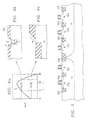
- Figures 1a-f illustrate in cross-sectional elevation views steps of the first preferred embodiment method of forming a trench isolation structure.
- Figures 1a-1f only show a single trench and do not show any doped wells or epilayers in the silicon substrate.
- Figure la shows silicon substrate 102 with overlying 10 nm thick pad silicon dioxide layer 104, 200 nm thick silicon nitride layer 106, and patterned photoresist 108.
- Pad oxide 104 may be deposited or thermally grown, and nitride 106 may be deposited.
- Photoresist 108 would be about 1 ⁇ m thick and patterned to expose the portions of silicon substrate to be etched to form the isolation trenches.
- the trenches may be 0.3 ⁇ m wide.
- Figure 1b illustrates the results of plasma etching with a chlorine based chemistry of the structure of Figure 1a .
- the trench etched into silicon substrate 102 may be 0.5 ⁇ m deep and have a sidewall slope of 75 degrees.
- trench 110 may have an aspect ratio of roughly 2:1. Avoid channel stop implants into the trench sidewalls because these will reduce the adjacent active device areas.
- Figure 1c shows stripping of photoresist 108 followed by a 20 nm thick thermal oxidation 114 of trench 110 sidewalls and bottom.
- the oxidation may be at 900°C with a 5%. HCl atmosphere. This oxidation also rounds trench 110 corners at the substrate surface, but nitride 106 prevents further oxidation.
- Pad oxide 104 and nitride 106 will form a polish stopping layer for later chemical mechanical polishing of the insulating material used to fill trenches 110.
- Pad oxide 104, nitride 106, and thermal oxide 114 form a continuous coating of silicon substrate 102 and protects against plasma ion bombardment in trench 110 filling step.
- the trenched substrate into inductively coupled high-density plasma reactor 200, such as illustrated in Figure 2 .
- deposit 0.9 ⁇ m of oxide 120 by plasma-enhanced deposition using source gases silane, oxygen, and argon diluent; see Figure 1d .
- Plasma heating increases the substrate temperature which is held by cooling at about 330°C.
- the source gas flows are about 30 sccm SiH 4 , 40 sccm O 2 , and 20 sccm Ar.
- the total pressure in the reaction chamber is about 4 mTorr; but despite the low pressure, the ion density is about 10 13 /cm 3 for reactor 200 and the oxide deposits at about 300 nm/min. Indeed, the deposited oxide has high quality and does not need a high temperature densification or cure anneal.
- the high ion density derives from the inductive coupling of rf source 201 with the feed gasses rather than the traditional capacitive coupling or ECR coupling.
- the inductive coupling in reactor 200 allows adjustment of the bias rf capacitive voltage (which determines plasma potential for ion bombardment of the substrate) between the plasma and the substrate on chuck 202 without affecting the plasma density.
- Set the bias about 1250 volts; this yields a deposition to sputter ratio of about 3.4 (for surfaces tilted 0 degrees from the ion bombardment direction). This insures filling trenches 110 without removal of oxide 104-114 and exposure of silicon substrate 102 along trench 110 sidewall tops to plasma ion bombardment; this limits leakage along trench 110 sidewalls.
- An alternative does not grow oxide 114 but rather begins trench 110 filling deposition with no bias to yield a conformal layer (no sputtering) of oxide without damage to silicon substrate 102 and then ramps up the bias voltage to insure trench 110 filling by oxide 120.
- the initial zero or low bias plasma enhanced deposition of oxide to a thickness of 20 nm provides the protective liner for trench sidewalls and the subsequent higher bias deposition fills the remainder of trench 110.
- Modifying the source gas flow rates and total pressure can change the deposition rate and the oxide quality.
- CMP chemical-mechanical polishing
- Figure 1f shows the final isolation structure. Subsequent processing will form transistors and other devices, insulating layers, and interconnection wirings to complete an integrated circuit.
- FIG. 2 shows reactor 200 in schematic cross sectional elevation view as including high density plasma (HDP) source 201 powered by an RF generator with a maximum of 3500 watts output, movable chuck 202 for holding wafers, and chamber 204.
- Chuck 202 has a helium backside gas feed for wafer temperature stability during processing and is powered by a capacitive RF generator with a maximum of 2000 watts output.
- Chuck 202 can hold a single 8 inch diameter wafer.
- Control of the RF power to HDP source 201 controls the plasma density
- control of the RF power to chuck 202 controls the bias developed between the plasma and the wafer and thus controls the ion energy for ions bombarding the wafer.
- the RF power to chuck 202 is small for the low bias deposition initial portion of the first preferred embodiment method and increases for the high bias deposition final portion.
- Figure 5 shows the first preferred embodiment trench isolation structure 502-512 for a twin-well CMOS integrated circuit with NMOS transistors 522-526 and PMOS transistors 532-534. Overlying insulation and interconnection layers have been omitted from Figure 5 for clarity.
- the preferred embodiments may be varied in many ways while retaining one or more of the features of inductively coupled high density plasma oxide filled trenches and use of the nitride etch mask portion as a CMP polish stopping layer.
- the dimensions of the trenches could be varied, such as 0.25-0.35 ⁇ m minimum width and 0.35-0.7 ⁇ m depth with sidewall slopes 70-80 degrees; the layer thicknesses could be varied, such as pad oxide thickness in the range 7-15 nm, nitride thickness 150-250 nm, and so forth; the source gasses for the oxide deposition could be varied and include silane, dichlorosilane, ozone, nitrous oxide, and so forth; the bias during plasma deposition could be ramped up from a low bias and still insure trench filling.
Landscapes
- Element Separation (AREA)
Applications Claiming Priority (2)
| Application Number | Priority Date | Filing Date | Title |
|---|---|---|---|
| US1968896P | 1996-06-10 | 1996-06-10 | |
| EP97109305A EP0813240B1 (fr) | 1996-06-10 | 1997-06-09 | Procédé de fabrication d'un circuit integré avec des tranchées d'isolation |
Related Parent Applications (2)
| Application Number | Title | Priority Date | Filing Date |
|---|---|---|---|
| EP97109305A Division EP0813240B1 (fr) | 1996-06-10 | 1997-06-09 | Procédé de fabrication d'un circuit integré avec des tranchées d'isolation |
| EP97109305.9 Division | 1997-06-09 |
Publications (2)
| Publication Number | Publication Date |
|---|---|
| EP2287901A2 true EP2287901A2 (fr) | 2011-02-23 |
| EP2287901A3 EP2287901A3 (fr) | 2014-05-07 |
Family
ID=21794537
Family Applications (2)
| Application Number | Title | Priority Date | Filing Date |
|---|---|---|---|
| EP97109305A Expired - Lifetime EP0813240B1 (fr) | 1996-06-10 | 1997-06-09 | Procédé de fabrication d'un circuit integré avec des tranchées d'isolation |
| EP10186092.2A Ceased EP2287901A3 (fr) | 1996-06-10 | 1997-06-09 | Améliorations associées aux dispositifs semi-conducteurs |
Family Applications Before (1)
| Application Number | Title | Priority Date | Filing Date |
|---|---|---|---|
| EP97109305A Expired - Lifetime EP0813240B1 (fr) | 1996-06-10 | 1997-06-09 | Procédé de fabrication d'un circuit integré avec des tranchées d'isolation |
Country Status (6)
| Country | Link |
|---|---|
| US (1) | US6313010B1 (fr) |
| EP (2) | EP0813240B1 (fr) |
| JP (1) | JP4195734B2 (fr) |
| KR (1) | KR100655845B1 (fr) |
| DE (1) | DE69740022D1 (fr) |
| TW (1) | TW388096B (fr) |
Families Citing this family (40)
| Publication number | Priority date | Publication date | Assignee | Title |
|---|---|---|---|---|
| US7235856B1 (en) * | 1997-12-18 | 2007-06-26 | Micron Technology, Inc. | Trench isolation for semiconductor devices |
| US6228741B1 (en) | 1998-01-13 | 2001-05-08 | Texas Instruments Incorporated | Method for trench isolation of semiconductor devices |
| JP3262059B2 (ja) | 1998-02-12 | 2002-03-04 | 日本電気株式会社 | 半導体装置の製造方法 |
| US6194038B1 (en) | 1998-03-20 | 2001-02-27 | Applied Materials, Inc. | Method for deposition of a conformal layer on a substrate |
| JPH11284060A (ja) * | 1998-03-27 | 1999-10-15 | Hitachi Ltd | 半導体装置及びその製造方法 |
| US6759306B1 (en) * | 1998-07-10 | 2004-07-06 | Micron Technology, Inc. | Methods of forming silicon dioxide layers and methods of forming trench isolation regions |
| US6573152B1 (en) | 1999-10-12 | 2003-06-03 | Stmicroelectronics S.R.L. | Self-planarizing process for shallow trench isolation |
| KR20010102310A (ko) | 1999-12-24 | 2001-11-15 | 롤페스 요하네스 게라투스 알베르투스 | 매립된 절연층상에 위치한 실리콘 웨이퍼의 상부층에형성된 반도체 소자를 포함하는 반도체 장치의 제조방법 |
| KR100419753B1 (ko) * | 1999-12-30 | 2004-02-21 | 주식회사 하이닉스반도체 | 반도체소자의 소자분리막 형성방법 |
| US6762129B2 (en) * | 2000-04-19 | 2004-07-13 | Matsushita Electric Industrial Co., Ltd. | Dry etching method, fabrication method for semiconductor device, and dry etching apparatus |
| US6559026B1 (en) * | 2000-05-25 | 2003-05-06 | Applied Materials, Inc | Trench fill with HDP-CVD process including coupled high power density plasma deposition |
| US6437417B1 (en) * | 2000-08-16 | 2002-08-20 | Micron Technology, Inc. | Method for making shallow trenches for isolation |
| KR100797385B1 (ko) * | 2000-10-19 | 2008-01-24 | 로베르트 보쉬 게엠베하 | 유도 결합 플라즈마를 이용한 기판의 에칭 장치 및 방법 |
| US6458722B1 (en) * | 2000-10-25 | 2002-10-01 | Applied Materials, Inc. | Controlled method of silicon-rich oxide deposition using HDP-CVD |
| US6596653B2 (en) | 2001-05-11 | 2003-07-22 | Applied Materials, Inc. | Hydrogen assisted undoped silicon oxide deposition process for HDP-CVD |
| US6740601B2 (en) | 2001-05-11 | 2004-05-25 | Applied Materials Inc. | HDP-CVD deposition process for filling high aspect ratio gaps |
| DE10127622B4 (de) * | 2001-06-07 | 2009-10-22 | Qimonda Ag | Verfahren zur Herstellung eines mit HDPCVD-Oxid gefüllten Isolationsgrabens |
| US6812064B2 (en) * | 2001-11-07 | 2004-11-02 | Micron Technology, Inc. | Ozone treatment of a ground semiconductor die to improve adhesive bonding to a substrate |
| US6812153B2 (en) * | 2002-04-30 | 2004-11-02 | Applied Materials Inc. | Method for high aspect ratio HDP CVD gapfill |
| US7628897B2 (en) * | 2002-10-23 | 2009-12-08 | Applied Materials, Inc. | Reactive ion etching for semiconductor device feature topography modification |
| JP2004193585A (ja) | 2002-11-29 | 2004-07-08 | Fujitsu Ltd | 半導体装置の製造方法と半導体装置 |
| US7097886B2 (en) * | 2002-12-13 | 2006-08-29 | Applied Materials, Inc. | Deposition process for high aspect ratio trenches |
| US6808748B2 (en) * | 2003-01-23 | 2004-10-26 | Applied Materials, Inc. | Hydrogen assisted HDP-CVD deposition process for aggressive gap-fill technology |
| US7081414B2 (en) * | 2003-05-23 | 2006-07-25 | Applied Materials, Inc. | Deposition-selective etch-deposition process for dielectric film gapfill |
| US6958112B2 (en) | 2003-05-27 | 2005-10-25 | Applied Materials, Inc. | Methods and systems for high-aspect-ratio gapfill using atomic-oxygen generation |
| US7354834B2 (en) * | 2003-06-04 | 2008-04-08 | Dongbu Electronics Co., Ltd. | Semiconductor devices and methods to form trenches in semiconductor devices |
| US7205240B2 (en) | 2003-06-04 | 2007-04-17 | Applied Materials, Inc. | HDP-CVD multistep gapfill process |
| US6903031B2 (en) * | 2003-09-03 | 2005-06-07 | Applied Materials, Inc. | In-situ-etch-assisted HDP deposition using SiF4 and hydrogen |
| US7087497B2 (en) * | 2004-03-04 | 2006-08-08 | Applied Materials | Low-thermal-budget gapfill process |
| JP2005340327A (ja) | 2004-05-25 | 2005-12-08 | Renesas Technology Corp | 半導体装置及びその製造方法 |
| US7229931B2 (en) | 2004-06-16 | 2007-06-12 | Applied Materials, Inc. | Oxygen plasma treatment for enhanced HDP-CVD gapfill |
| US7183227B1 (en) | 2004-07-01 | 2007-02-27 | Applied Materials, Inc. | Use of enhanced turbomolecular pump for gapfill deposition using high flows of low-mass fluent gas |
| US7087536B2 (en) | 2004-09-01 | 2006-08-08 | Applied Materials | Silicon oxide gapfill deposition using liquid precursors |
| JP4961668B2 (ja) * | 2005-01-11 | 2012-06-27 | 富士電機株式会社 | 半導体装置の製造方法 |
| KR100767333B1 (ko) * | 2006-05-24 | 2007-10-17 | 한국과학기술연구원 | 계면 제어층을 포함하는 비휘발성 전기적 상변화 메모리소자 및 이의 제조방법 |
| JP2008060266A (ja) * | 2006-08-30 | 2008-03-13 | Oki Electric Ind Co Ltd | 素子分離膜の形成方法と不揮発性半導体メモリ |
| US7678715B2 (en) | 2007-12-21 | 2010-03-16 | Applied Materials, Inc. | Low wet etch rate silicon nitride film |
| US8497211B2 (en) | 2011-06-24 | 2013-07-30 | Applied Materials, Inc. | Integrated process modulation for PSG gapfill |
| JP5859758B2 (ja) * | 2011-07-05 | 2016-02-16 | ルネサスエレクトロニクス株式会社 | 半導体装置の製造方法 |
| US9018108B2 (en) | 2013-01-25 | 2015-04-28 | Applied Materials, Inc. | Low shrinkage dielectric films |
Citations (1)
| Publication number | Priority date | Publication date | Assignee | Title |
|---|---|---|---|---|
| EP0552491A1 (fr) * | 1992-01-24 | 1993-07-28 | Applied Materials, Inc. | Procédé de gravure par plasma |
Family Cites Families (11)
| Publication number | Priority date | Publication date | Assignee | Title |
|---|---|---|---|---|
| US5094972A (en) * | 1990-06-14 | 1992-03-10 | National Semiconductor Corp. | Means of planarizing integrated circuits with fully recessed isolation dielectric |
| US5290396A (en) * | 1991-06-06 | 1994-03-01 | Lsi Logic Corporation | Trench planarization techniques |
| US5397962A (en) * | 1992-06-29 | 1995-03-14 | Texas Instruments Incorporated | Source and method for generating high-density plasma with inductive power coupling |
| US5494857A (en) * | 1993-07-28 | 1996-02-27 | Digital Equipment Corporation | Chemical mechanical planarization of shallow trenches in semiconductor substrates |
| US5614055A (en) | 1993-08-27 | 1997-03-25 | Applied Materials, Inc. | High density plasma CVD and etching reactor |
| JP3438446B2 (ja) * | 1995-05-15 | 2003-08-18 | ソニー株式会社 | 半導体装置の製造方法 |
| US5719085A (en) * | 1995-09-29 | 1998-02-17 | Intel Corporation | Shallow trench isolation technique |
| KR100214068B1 (ko) * | 1995-11-21 | 1999-08-02 | 김영환 | 반도체 장치의 소자분리막 형성방법 |
| EP0870327B1 (fr) * | 1995-12-27 | 2002-09-11 | Lam Research Corporation | Procede de remplissage de tranchees dans une plaquette a semiconducteur |
| US5851899A (en) * | 1996-08-08 | 1998-12-22 | Siemens Aktiengesellschaft | Gapfill and planarization process for shallow trench isolation |
| US5728621A (en) * | 1997-04-28 | 1998-03-17 | Chartered Semiconductor Manufacturing Pte Ltd | Method for shallow trench isolation |
-
1997
- 1997-06-06 JP JP14972497A patent/JP4195734B2/ja not_active Expired - Lifetime
- 1997-06-06 TW TW086107788A patent/TW388096B/zh not_active IP Right Cessation
- 1997-06-09 US US08/871,738 patent/US6313010B1/en not_active Expired - Lifetime
- 1997-06-09 EP EP97109305A patent/EP0813240B1/fr not_active Expired - Lifetime
- 1997-06-09 EP EP10186092.2A patent/EP2287901A3/fr not_active Ceased
- 1997-06-09 DE DE69740022T patent/DE69740022D1/de not_active Expired - Lifetime
- 1997-06-10 KR KR1019970023849A patent/KR100655845B1/ko not_active Expired - Lifetime
Patent Citations (1)
| Publication number | Priority date | Publication date | Assignee | Title |
|---|---|---|---|---|
| EP0552491A1 (fr) * | 1992-01-24 | 1993-07-28 | Applied Materials, Inc. | Procédé de gravure par plasma |
Non-Patent Citations (1)
| Title |
|---|
| GOSHO ET AL.: "Trench Isolation Technology for 0.35 µm Devices by Bias ECR CVD", VLSI SYMP TECH DIGEST 87, 1991 |
Also Published As
| Publication number | Publication date |
|---|---|
| JP4195734B2 (ja) | 2008-12-10 |
| TW388096B (en) | 2000-04-21 |
| EP0813240A1 (fr) | 1997-12-17 |
| KR100655845B1 (ko) | 2007-04-11 |
| EP2287901A3 (fr) | 2014-05-07 |
| US6313010B1 (en) | 2001-11-06 |
| JPH1056058A (ja) | 1998-02-24 |
| EP0813240B1 (fr) | 2010-10-13 |
| DE69740022D1 (de) | 2010-11-25 |
| KR980006113A (ko) | 1998-03-30 |
Similar Documents
| Publication | Publication Date | Title |
|---|---|---|
| EP0813240B1 (fr) | Procédé de fabrication d'un circuit integré avec des tranchées d'isolation | |
| US6211040B1 (en) | Two-step, low argon, HDP CVD oxide deposition process | |
| US5985735A (en) | Trench isolation process using nitrogen preconditioning to reduce crystal defects | |
| US6001706A (en) | Method for making improved shallow trench isolation for semiconductor integrated circuits | |
| US7176138B2 (en) | Selective nitride liner formation for shallow trench isolation | |
| KR102514465B1 (ko) | 유전체 재료를 증착하기 위한 방법들 | |
| US9209243B2 (en) | Method of forming a shallow trench isolation structure | |
| US8216913B2 (en) | Strain modulation in active areas by controlled incorporation of nitrogen at si-SiO2 interface | |
| WO1986002777A1 (fr) | Procede de formation de zones d'isolation dans un substrat de semi-conducteurs | |
| US7202123B1 (en) | Mesa isolation technology for extremely thin silicon-on-insulator semiconductor devices | |
| US6534379B1 (en) | Linerless shallow trench isolation method | |
| US6214697B1 (en) | Trench isolation for semiconductor devices | |
| US6306725B1 (en) | In-situ liner for isolation trench side walls and method | |
| US6143625A (en) | Protective liner for isolation trench side walls and method | |
| US6602759B2 (en) | Shallow trench isolation for thin silicon/silicon-on-insulator substrates by utilizing polysilicon | |
| US6051480A (en) | Trench isolation for semiconductor devices | |
| US6333218B1 (en) | Method of etching contacts with reduced oxide stress | |
| US5739575A (en) | Dielectrically isolated substrate and method for manufacturing the same | |
| KR100325615B1 (ko) | 다층 주입 공정을 이용한 반도체 소자 제조 방법 | |
| US7981800B1 (en) | Shallow trench isolation structures and methods for forming the same | |
| KR100379524B1 (ko) | 반도체 소자의 격리막 형성 방법 | |
| KR100624330B1 (ko) | 소자분리 구조 형성 방법 | |
| KR20010019280A (ko) | 얕은 트렌치 소자분리 방법 | |
| CN121126857A (zh) | 一种半导体器件的制备方法及半导体器件 | |
| JP3980866B2 (ja) | 半導体デバイスの製造方法 |
Legal Events
| Date | Code | Title | Description |
|---|---|---|---|
| PUAI | Public reference made under article 153(3) epc to a published international application that has entered the european phase |
Free format text: ORIGINAL CODE: 0009012 |
|
| AC | Divisional application: reference to earlier application |
Ref document number: 0813240 Country of ref document: EP Kind code of ref document: P |
|
| AK | Designated contracting states |
Kind code of ref document: A2 Designated state(s): DE FR GB IT NL |
|
| PUAL | Search report despatched |
Free format text: ORIGINAL CODE: 0009013 |
|
| AK | Designated contracting states |
Kind code of ref document: A3 Designated state(s): DE FR GB IT NL |
|
| RIC1 | Information provided on ipc code assigned before grant |
Ipc: H01L 21/762 20060101AFI20140331BHEP |
|
| 17P | Request for examination filed |
Effective date: 20141107 |
|
| RBV | Designated contracting states (corrected) |
Designated state(s): DE FR GB IT NL |
|
| 17Q | First examination report despatched |
Effective date: 20180601 |
|
| STAA | Information on the status of an ep patent application or granted ep patent |
Free format text: STATUS: THE APPLICATION HAS BEEN REFUSED |
|
| 18R | Application refused |
Effective date: 20191107 |