EP2297976B1 - Piezoelektrisches mems-mikrofon - Google Patents
Piezoelektrisches mems-mikrofon Download PDFInfo
- Publication number
- EP2297976B1 EP2297976B1 EP09774338.9A EP09774338A EP2297976B1 EP 2297976 B1 EP2297976 B1 EP 2297976B1 EP 09774338 A EP09774338 A EP 09774338A EP 2297976 B1 EP2297976 B1 EP 2297976B1
- Authority
- EP
- European Patent Office
- Prior art keywords
- piezoelectric
- sensor
- layer
- mems microphone
- beams
- Prior art date
- Legal status (The legal status is an assumption and is not a legal conclusion. Google has not performed a legal analysis and makes no representation as to the accuracy of the status listed.)
- Active
Links
Images


Classifications
-
- H—ELECTRICITY
- H10—SEMICONDUCTOR DEVICES; ELECTRIC SOLID-STATE DEVICES NOT OTHERWISE PROVIDED FOR
- H10N—ELECTRIC SOLID-STATE DEVICES NOT OTHERWISE PROVIDED FOR
- H10N30/00—Piezoelectric or electrostrictive devices
- H10N30/50—Piezoelectric or electrostrictive devices having a stacked or multilayer structure
-
- H—ELECTRICITY
- H04—ELECTRIC COMMUNICATION TECHNIQUE
- H04R—LOUDSPEAKERS, MICROPHONES, GRAMOPHONE PICK-UPS OR LIKE ACOUSTIC ELECTROMECHANICAL TRANSDUCERS; ELECTRIC HEARING AIDS; PUBLIC ADDRESS SYSTEMS
- H04R17/00—Piezoelectric transducers; Electrostrictive transducers
- H04R17/10—Resonant transducers, i.e. adapted to produce maximum output at a predetermined frequency
-
- H—ELECTRICITY
- H04—ELECTRIC COMMUNICATION TECHNIQUE
- H04R—LOUDSPEAKERS, MICROPHONES, GRAMOPHONE PICK-UPS OR LIKE ACOUSTIC ELECTROMECHANICAL TRANSDUCERS; ELECTRIC HEARING AIDS; PUBLIC ADDRESS SYSTEMS
- H04R17/00—Piezoelectric transducers; Electrostrictive transducers
- H04R17/02—Microphones
-
- B—PERFORMING OPERATIONS; TRANSPORTING
- B81—MICROSTRUCTURAL TECHNOLOGY
- B81B—MICROSTRUCTURAL DEVICES OR SYSTEMS, e.g. MICROMECHANICAL DEVICES
- B81B3/00—Devices comprising flexible or deformable elements, e.g. comprising elastic tongues or membranes
- B81B3/0018—Structures acting upon the moving or flexible element for transforming energy into mechanical movement or vice versa, i.e. actuators, sensors, generators
- B81B3/0021—Transducers for transforming electrical into mechanical energy or vice versa
-
- B—PERFORMING OPERATIONS; TRANSPORTING
- B81—MICROSTRUCTURAL TECHNOLOGY
- B81C—PROCESSES OR APPARATUS SPECIALLY ADAPTED FOR THE MANUFACTURE OR TREATMENT OF MICROSTRUCTURAL DEVICES OR SYSTEMS
- B81C1/00—Manufacture or treatment of devices or systems in or on a substrate
- B81C1/00015—Manufacture or treatment of devices or systems in or on a substrate for manufacturing microsystems
- B81C1/00134—Manufacture or treatment of devices or systems in or on a substrate for manufacturing microsystems comprising flexible or deformable structures
- B81C1/0015—Cantilevers
-
- B—PERFORMING OPERATIONS; TRANSPORTING
- B81—MICROSTRUCTURAL TECHNOLOGY
- B81C—PROCESSES OR APPARATUS SPECIALLY ADAPTED FOR THE MANUFACTURE OR TREATMENT OF MICROSTRUCTURAL DEVICES OR SYSTEMS
- B81C1/00—Manufacture or treatment of devices or systems in or on a substrate
- B81C1/00015—Manufacture or treatment of devices or systems in or on a substrate for manufacturing microsystems
- B81C1/00134—Manufacture or treatment of devices or systems in or on a substrate for manufacturing microsystems comprising flexible or deformable structures
- B81C1/00158—Diaphragms, membranes
-
- H—ELECTRICITY
- H04—ELECTRIC COMMUNICATION TECHNIQUE
- H04R—LOUDSPEAKERS, MICROPHONES, GRAMOPHONE PICK-UPS OR LIKE ACOUSTIC ELECTROMECHANICAL TRANSDUCERS; ELECTRIC HEARING AIDS; PUBLIC ADDRESS SYSTEMS
- H04R17/00—Piezoelectric transducers; Electrostrictive transducers
-
- H—ELECTRICITY
- H10—SEMICONDUCTOR DEVICES; ELECTRIC SOLID-STATE DEVICES NOT OTHERWISE PROVIDED FOR
- H10N—ELECTRIC SOLID-STATE DEVICES NOT OTHERWISE PROVIDED FOR
- H10N30/00—Piezoelectric or electrostrictive devices
- H10N30/01—Manufacture or treatment
- H10N30/05—Manufacture of multilayered piezoelectric or electrostrictive devices, or parts thereof, e.g. by stacking piezoelectric bodies and electrodes
-
- H—ELECTRICITY
- H10—SEMICONDUCTOR DEVICES; ELECTRIC SOLID-STATE DEVICES NOT OTHERWISE PROVIDED FOR
- H10N—ELECTRIC SOLID-STATE DEVICES NOT OTHERWISE PROVIDED FOR
- H10N30/00—Piezoelectric or electrostrictive devices
- H10N30/30—Piezoelectric or electrostrictive devices with mechanical input and electrical output, e.g. functioning as generators or sensors
- H10N30/302—Sensors
-
- H—ELECTRICITY
- H10—SEMICONDUCTOR DEVICES; ELECTRIC SOLID-STATE DEVICES NOT OTHERWISE PROVIDED FOR
- H10N—ELECTRIC SOLID-STATE DEVICES NOT OTHERWISE PROVIDED FOR
- H10N30/00—Piezoelectric or electrostrictive devices
- H10N30/30—Piezoelectric or electrostrictive devices with mechanical input and electrical output, e.g. functioning as generators or sensors
- H10N30/304—Beam type
- H10N30/306—Cantilevers
-
- B—PERFORMING OPERATIONS; TRANSPORTING
- B81—MICROSTRUCTURAL TECHNOLOGY
- B81B—MICROSTRUCTURAL DEVICES OR SYSTEMS, e.g. MICROMECHANICAL DEVICES
- B81B2201/00—Specific applications of microelectromechanical systems
- B81B2201/02—Sensors
- B81B2201/0257—Microphones or microspeakers
-
- H—ELECTRICITY
- H04—ELECTRIC COMMUNICATION TECHNIQUE
- H04R—LOUDSPEAKERS, MICROPHONES, GRAMOPHONE PICK-UPS OR LIKE ACOUSTIC ELECTROMECHANICAL TRANSDUCERS; ELECTRIC HEARING AIDS; PUBLIC ADDRESS SYSTEMS
- H04R2201/00—Details of transducers, loudspeakers or microphones covered by H04R1/00 but not provided for in any of its subgroups
- H04R2201/003—Mems transducers or their use
Definitions
- This invention relates generally to piezoelectric microphones and, in particular, to piezoelectric MEMS microphones and design techniques for constructing such microphones to meet the requirements of a particular end use application.
- MEMS microelectromechanical systems
- acoustic transducers such as microphones using silicon-wafer deposition techniques.
- Microphones fabricated this way are commonly referred to as MEMS microphones and can be made in various forms such as capacitive microphones or piezoelectric microphones using a material such as PZT, ZnO, PVDF, PMN-PT, or AlN.
- MEMS capacitive microphones and electret condenser microphones (ECMs) are used in consumer electronics and have an advantage over typical piezoelectric MEMS microphones in that they have greater sensitivity and lower noise floors.
- ECMs electret condenser microphones
- MEMS capacitive microphones which are often used in cell phones, are relatively expensive due at least in part to the use of an application-specific integrated circuit (ASIC) that provides readout circuitry for the microphone. MEMS capacitive microphones also have a smaller dynamic range than typical piezoelectric MEMS microphones.
- ASIC application-specific integrated circuit
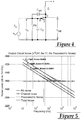
- Fig. 1 The noise floors of various known piezoelectric and capacitive MEMS microphones are shown in Fig. 1 . As indicated by the two encircled groups of microphones, capacitive MEMS microphones (the lower group) generally have a noise floor that is about 20dB lower than similarly sized piezoelectric MEMS microphones.
- piezoelectric MEMS microphones have been made either as cantilevered beams or as a diaphragm, and these microphones include both electrodes and the piezoelectric material along with a structural material such as Parylene or silicon that is used as a diaphragm or beam substrate material.
- Parylene for cantilever designs is that it is can be used to increase the thickness of the beam which both increases the bandwidth of the beam (for a fixed length) and increases the distance from the neutral axis of the piezoelectric material, which seemingly increases sensitivity.
- beam substrates of about 20 ⁇ m are known, see Ledermann [15].
- thinner layers have been used for piezoelectric MEMS microphones that utilize a Parylene diaphragm.
- the senor comprises a plurality of beams each supported at one end by the substrate such that each beam is cantilevered and extends between a fixed end and a free end.
- Each beam comprises a deposited layer of electrode material and a deposited layer of piezoelectric material overlying the electrode material. At least some of the beams are stacked such that the stacked beams include alternative layers of deposited electrode material and deposited piezoelectric material with no additional layers therebetween.
- the senor comprises a stress-relieved diaphragm suspended above the substrate.
- the diaphragm may have at least three layers including a first electrode layer, an intermediate layer of piezoelectric material deposited over the first electrode layer, and a second electrode layer deposited over the piezoelectric material.
- the stress relieved diaphragm can be obtained in any suitable manner, such as for example, by detaching it from the substrate about substantially all of its periphery and allowing it to expand or contract as needed to relieve residual stress. The diaphragm can then be reattached to the substrate about its periphery by any suitable technique.
- Typical piezoelectric MEMS microphones are designed so as to optimize sensitivity of the microphone, and this is at least partially responsible for the increased noise floors noted above for these devices.
- a piezoelectric MEMS microphone can be constructed that has sufficient sensitivity for typical applications along with a noise floor similar to that of capacitive MEMS microphones.
- This approach is valid for films of good quality. However, as the film is reduced in thickness, the film quality will degrade. This factor can be accounted for with an alternative approach described herein which utilizes a calculated optimization parameter that is still a ratio of sensor energy to area, but also includes the pressure, natural frequency (which limits the bandwidth), and the loss angle of the device.
- V out the output voltage
- C the device capacitance
- P the input pressure
- A the sensor area
- tan( ⁇ ) is the dielectric loss angle or dissipation factor of the microphone at the first resonant frequency
- f res is the first resonant frequency of the device.
- a first is the use of sensor structures, such as diaphragms, that have their stiffness dominated by tension.
- this tension is the result of residual stress left on each layer after deposition. This effect leads to a reduction in normalized output energy, one of the elements of the optimization parameter, as can be seen in Fig. 2 .
- This figure shows how residual stress reduces the normalized output energy of a diaphragm with two 1 ⁇ m aluminum nitride (AlN) layers and three 100 nm molybdenum (Mo) layers with 20 kHz resonant frequency.
- AlN aluminum nitride
- Mo molybdenum
- these problems can be addressed in one or more ways.
- this can be done by utilizing a microphone design that achieves at least 10% of the maximum ratio obtainable of output energy to sensor area for a given input pressure, bandwidth, and piezoelectric material.
- the "maximum ratio obtainable" for a given sensor design can be determined using an output energy calculation along with sensor area, or can be determined using the optimization parameter equation given above along with available (albeit sometimes varying) values and equations for the various parameters used in the optimization equation. In this latter approach, suitable sensor designs can be obtained for which the calculated optimization parameter is at least 10% of the maximum obtainable optimization parameter for the sensor.
- an improved piezoelectric MEMS microphone can be built using a stress-relieved diaphragm, in which the piezoelectric sensor is made by deposition on a silicon-based substrate, then released from the substrate to permit expansion or contraction of the released membrane to relieve any residual stress, and then re-attached in any suitable manner.
- This technique could work for a diaphragm with any combination of clamped, pinned, or free perimeter conditions.
- Use of the optimization calculation above can also be used in making the diaphragm piezoelectric MEMS microphone to provide enhanced microphone sensitivity and noise performance.
- cantilever and diaphragm designs provide useful operation of the device for many applications, and designs for which the calculated optimization parameter is above 10% of optimal can provide enhanced operation that provides good sensitivity with noise floors per unit area that are on par with or exceeding that of capacitive MEMS microphones.
- Fig. 3a depicts a beam cantilevered piezoelectric MEMS microphone 30 that comprises a multi-layer acoustic sensor having a plurality of fingered beams 32, each cantilevered at one of the two left and right sides 34, 36 of the microphone such the free ends of each facing pair of beams 32 are separated by a small gap 38 that can be formed using known MEMS manufacturing technology.
- this gap is no greater than 3 ⁇ m, but can be larger depending on the design. For most applications, a gap of no greater than 10 ⁇ m can be used.
- a similar gap 40 can be used between adjacent (side-by-side) beams. Cantilevering of the beams 32 reduces the influence of material residual stress on the device bandwidth.
- each beam 32 shown can be the upper beam of a stacked set of two or more beams formed by alternating layers of electrode and piezoelectric material.
- there are five alternating layers although it will be appreciated that, for a stacked beam configuration, additional layers could be used.
- These beams are constructed without any other layers or materials such that the beams comprise only electrode and piezoelectric layers.
- the electrode material is molybdenum and the piezoelectric material is aluminum nitride; however, it will be appreciated that any suitable conductive material can be used for the electrodes (e.g., titanium) and any suitable piezoelectric material can be used, such as PZT, ZnO, or others.
- the beams 32 can have dimensions determined according to the design methodology described below to provide a desirable set of characteristics.
- the the piezoelectric layer can be under 1 ⁇ m, and more preferably, about 0.5 ⁇ m, although again this will vary based on a number of factors, including other beam dimensions, materials, etc.
- the beam thickness, and thus the piezoelectric thickness will be less than 2 ⁇ m, but can go as high as 8 ⁇ m depending upon the particular application involved.
- the piezoelectric layer thickness is made as thin as possible while maintaining good piezoelectric film quality.
- the layer can be made as thin as the available manufacturing technology makes possible as long as it has sufficient thickness to exhibit a sufficient piezoelectric effect for the particular application involved.
- the beam length should be related to the thickness, as indicated in the design description below.
- the electrode layer can vary as well, but preferably is on the order of 0.2 ⁇ m or less.
- the base end of the beams are supported with a minimal amount of area to help minimize the resulting capacitance.
- the MEMS microphone 30 has several advantageous features, any one or more of which can be achieved using the design methodologies described herein. These features include:
- the design of the cantilever microphone 30 for any particular application can be carried out using the design methodology described below.
- This methodology was developed based on mathematical modeling of the beams that was primarily done analytically and verified experimentally.
- ⁇ is the density averaged through the thickness
- A is the cross-sectional area
- w is the beam deflection
- t is time
- x is the distance along the beam
- M is the beam bending moment
- f is the force per unit width
- b is the beam width
- N is the number of layers l
- s is the elastic material compliance
- d is a piezoelectric coupling coefficient
- ⁇ is the electric permittivity
- z is the height from the bottom of the beam as seen in Fig. 3c
- V is the voltage across the layer.
- V the voltage, in the moment equation can be determined by extending the method of Irschik [2] to multiple layers resulting in:
- V l ⁇ d 31 l s 11 l ⁇ 33 l ⁇ d 31 l 2 1 2 z l ⁇ z o 2 ⁇ z l ⁇ 1 ⁇ z o 2 1
- V l z l ⁇ z l ⁇ 1 ⁇ l 1 N 1 s 11 l z l ⁇ z l ⁇ 1
- C l ⁇ 33 l bL z l ⁇ z l ⁇ 1 .
- the device output energy (referred to as the output energy) will be the sum of the output energy of each layer provided that the beams 32 are wired in any combination of series or parallel that preserves this product.
- the parameters of the beam layup e.g., layer height and length
- This ratio is: OutputEnergy SensorArea .
- sensor area refers to the total chip surface area comprising piezoelectric beams.
- the microphone 30 is designed and constructed to achieve as close to the maximum achievable value as possible. However, owing to a variety of reasons (e.g., cost of construction), designs of even as low as 10% of the optimal energy to sensor area ratios may be acceptable for certain applications.
- the noise floor (minimum detectable signal) of the piezoelectric microphone 30 is limited fundamentally by the dielectric loss angle of the material as described by Levinzon [6].
- This determines the output voltage noise of a given beam 32 or combination of beams.
- Other noise sources such as mechanical thermal noise from the beams, radiation impedance of the beams, and 1/f noise do not dominate the noise of the microphone.
- the amplification electronics could be anything ranging from a charge amplifier to an integrated circuit for voltage amplification.
- the demonstrated device uses a junction field effect transistor (JFET) in a common source amplifier with a load resistor of 2.2 k ⁇ for amplification because these transistors have relatively low noise, are small, inexpensive, and relatively simple to model.
- JFET noise can be modeled as shown by Levinzon [7]. At low frequencies, the thermal noise of the resistor R b , shown in Fig. 4 , dominates the circuit.
- R b dominates the resistance
- C moves the pole to a lower frequency and therefore further attenuates the thermal noise.
- a typical noise curve for a piezoelectric sensor connected to a JFET is shown in Fig. 5 .
- the dynamic range of the microphone 30 exceeds the requirements for most applications and will typically be limited by the electronics to which it is connected.
- the microphone 30 itself consumes no power so the total power consumption is dependent on that of the amplification circuitry.
- the area of the microphone is determined by the size and number of beams used and can be traded off with noise floor, sensitivity, and bandwidth.
- the sensitivity of this microphone 30 to other parameters such as vibration and temperature has also been investigated.
- this device 30 uses multiple beams 32, they can be connected in either series or parallel but the output energy, the product V 2 C, remains constant for a given acoustic pressure as noted by Ried [9].
- the method by which these beams are connected illustrates the trade-off between sensitivity and noise. If they are all connected in series, this maximizes sensitivity but the sensor capacitance, C, will be very small. If a JFET is used for amplification, this will increase the frequency of the pole filtering the noise and the resulting noise will increase. In general, a small capacitance will be detrimental because the input capacitance to the electronics will act as a capacitive divider and reduce the signal. If all the beams are connected in parallel, this results in the minimum sensitivity but maximum sensor capacitance. An optimal capacitance, usually between the two limiting cases discussed above (all parallel v. all series), can be identified to minimize the input referred noise of the system when using a JFET.
- area can be traded off with sensitivity and noise floor. More beams consume more area but result in a larger V 2 C product. Bandwidth can also be traded off with noise floor, sensitivity, and area. Longer beams consume more area but give a larger V 2 C product for a given area because they are more compliant. These longer beams have a lower natural frequency and, therefore, a lower bandwidth.
- Fig. 6 there are other design/construction factors that influence microphone output.
- beams having a width that is tapered toward their free ends can provide a greater V 2 C output energy. The peak value of this is at a beam base to tip ratio of about 0.33.
- a layer of Parylene interposed between the electrode and piezoelectric can provide a better V 2 C output.
- Fig. 7 was generated to determine the advantage/disadvantage of an intermediate layer of Parylene. This figure shows that a thin layer of Parylene does slightly enhance the V 2 C product of a constant area/ constant bandwidth group of beams.
- AlN was selected as the piezoelectric material because it gives equal or superior performance compared to other common MEMS piezoelectric materials such as ZnO and PZT but is more CMOS compatible than either of those two materials. It can be difficult to identify the optimal piezoelectric material because device performance will depend upon several material parameters such as d 31 , tan( ⁇ ), electric permittivity, s, and ⁇ . These properties depend upon material composition, deposition power/pressure/temperature, substrate roughness and crystal structure, material thickness, etc. In addition to material deposition variability, it can be difficult to find a source that provides all the necessary information for a complete material comparison as the quoted values for these parameters can vary substantially, more so for PZT than A1N because PZT has more variation in composition and orientation.
- Titanium (Ti), therefore works better than Mo but was not used because of compatibility issues with other processing steps.
- the thicknesses of the layers were selected because these were the thinnest that could be reasonably deposited with good quality. The models indicate that thinner layers would be beneficial but were not attempted in the fabrication.
- Figs. 9a-9d The processing of the device is shown in Figs. 9a-9d .
- a 200nm layer of SiO 2 was deposited as an etch stop for the DRIE etch.
- a 200nm layer of Mo was deposited, patterned, and etched with dilute Aqua Regia (9H 2 O:1HNO 3 :3HCL).
- a 500nm layer of A1N followed by a 200nm layer of Mo was deposited, patterned, and etched with dilute Aqua Regia for the Mo and hot (85C) H 3 PO 4 for the AlN.
- another 500nm AlN and 200nm Mo were deposited, patterned, and etched. All A1N depositions were performed at UC Berkeley by Harmonic Devices.
- a transistor outline can as seen in Fig. 11 and wire bonded to a JFET to buffer the signal. This can be done as indicated in Fig. 4 with the gate input of the JFET being connected to the sensor electrodes such that signals received from the electrodes are amplified by the transistor.
- a hole was drilled in the TO can below the microphone in order to give optical access to the beams and measure their deflection. This hole also allows the size of the back cavity to be adjusted, as the size of the back cavity will determine the low end of the microphone bandwidth.
- the microphone was then placed in a plane wave tube next to a reference microphone (Larsen Davis model 2520) and the frequency response was measured using a LabView A/D card and software. This can be seen in Fig. 12 .
- the d 31 coefficient was measured by actuating the beams and measuring the beam curvature with a laser vibrometer.
- the beam deflection profile can be seen in Fig. 13 .
- the natural frequency of the beams was determined by measuring the frequency response of the beams to actuation.
- Another parameter that influences the microphone performance is the dielectric loss angle tan( ⁇ ) of the microphone. This has been measured with both custom circuitry in conjunction with LabViewTM software and with an Agilent Model 4284A Precision LCR meter.
- the d 31 coefficient was measured as 1.68 x 10 -12 N/C. This value is about 65% of the best values quoted in the literature. The d 31 coefficient has been shown to correlate with the X-ray diffraction rocking curve FWHM which, for this layer, is about 2.6 degrees while the best reported are around 1 degree.
- Tan( ⁇ ) was measured as 0.04 at 1kHz.
- the literature typically gives tan( ⁇ ) in the range of 0.001 to 0.002 so this value is more than an order of magnitude higher than those typically quoted. It was determined that this higher than expected tan( ⁇ ) is due to some residual material left after etching the AlN with H 3 PO 4 . After some investigation, it was found that the tan( ⁇ ) can be reduced by cleaning with Acetone while in an ultrasound bath and heating on a hot plate. The devices with a lower tan( ⁇ ) will result in microphones with a lower noise floor.
- the microphone model matches the measured performance quite well.
- the sensitivity shown in Fig. 14 , is measured as 0.52mV/Pa out of the JFET common source amplifier with a 2.2kOhm load resistor. This equates to a raw output sensitivity of 0.17mV/Pa for the piezoelectric microphone.
- the model predicts an output sensitivity of 0.18mV/Pa.
- the measured input referred noise floor for the device is 58.2 dBA while the model predicts an input referred noise floor of 57.3 dBA.
- Fig. 14 shows the measured and predicted sensitivities and noise floors.
- the first peak in the measured frequency response is caused by the natural frequency of the beams across from those used in the measurement. They are not exactly the same length due to a non-uniformity in the DRIE etch.
- optimization of the output energy to sensor area ratio was determined based on a given input pressure, bandwidth, and piezoelectric material.
- these constraints can be taken into account in the design or analysis of a piezoelectric MEMS microphone.
- Optimization Parameter V out 2 C P 2 A tan ⁇ ⁇ f res 2 the input pressure can be accounted for by the pressure P term, the bandwidth by the f res term, and the characteristics of the piezoelectric material and the electrode by the dielectric loss angle tan( ⁇ ).
- the output energy to sensor area ratio can be optimized by maximizing the optimization parameter equation given above to take those other factors into account.
- the normalized output energy can be plotted as a function of electrode length as shown in Fig. 15 . As the normalized output energy per unit area increases, so will the optimization parameter so the electrode will go from the base of the beam to roughly 50% the length of the beam.
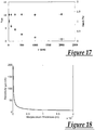
- the d 31 data can be extracted by assuming that the d 31 coefficient degrades at the same rate as the d 33 coefficient. Plots of d 33 and tan( ⁇ ) degradation are given in Martin [16] and are shown in Figs. 16 and 17 , respectively. Alternatively, the dependence of d 31 on thickness could be determined experimentally.
- the Mo conductivity will also change as the thickness is decreased.
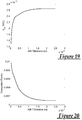
- the assumed relationships between Mo resistivity and Mo thickness, between d 31 and AlN thickness, and between loss angle and AlN thickness are shown in respective Figs. 18-20 .
- the ideal thicknesses for a three layer device are shown in Table 1 below. Table 1 Layer Thickness Molvbdenum #1 9 nm Aluminum Nitride 1.5 ⁇ m Molvbdenum #2 1.1 ⁇ m
- the fluid loading of air above and below a 1 mm x 1 mm diaphragm has been added to the density summation.
- the natural frequency equation can then be used to calculate the length of the beam. For a natural frequency of 20 kHz, the beam will be 374 ⁇ m long.
- the plots of Figs. 21-23 show the effect of changing any layer thickness on the optimization parameter. Small relative changes do not greatly affect the value of the optimization parameter except in the case of the bottom Mo thickness. For this reason, it may be wise to use a more conservative bottom Mo thickness such as 20 nm.
- electrode thicknesses of 50 nm, 100 nm or more can be used since, as shown in Figs. 18-20 the optimization parameter, particularly of the bottom electrode, does not decrease too substantially with thicknesses in this range.
- the desired sensor area is roughly 1 mm x 1 mm, this beam can be made to be 1 mm wide and three of them can be placed end to end.
- the natural frequency equation can then be used to calculate the length of the beam.
- the beam will be 461 ⁇ m.
- the plots of Figs. 24-26 show the effect of changing any layer thickness on the optimization parameter. Again, these plots show that the electrode layer can be increased significantly to, e.g., 20, 50, 100 nm or more without suffering too great a reduction in the calculated output voltage to sensor area ratio, and that the middle electrode can be varied between 5 nm and 1 ⁇ m without reducing the ratio to below 10% of its maximum obtainable value.
- a stress relieved diaphragm design can also provide a good combination of sensitivity and low noise floor.
- Figs. 27a and 27b there is shown a piezoelectric MEMS microphone 50 comprising a multi-layer acoustic sensor in the form of a stress-relieved diaphragm 52 suspended above a silicon substrate 54.
- a stress-relieved diaphragm 52 suspended above a silicon substrate 54.
- only three layers are used, upper and lower Mo electrode layers, and an intermediate layer of AlN piezoelectric material.
- Parylene and other material layers can also be used, and that the diaphragm can have multiple piezoelectric layers such as discussed above in connection with the stacked beam cantilever configurations.
- the illustrated embodiment includes only three layers, the upper and lower electrode layers are patterned to each define two independent electrodes.
- the first (lower) electrode layer includes a central electrode 56 and an outer ring shaped electrode 58 that surrounds the central electrode 56.
- the second (upper) electrode layer shown in Fig. 27a also includes a central electrode 57 and an outer ring shaped electrode 59 that surrounds the central electrode 57. From the perspective of the top view shown in Fig. 27a , both the central electrode 57 and outer ring electrode 59 are co-extensive with their associated lower central electrode 56 and ring electrode 58, respectively.
- the central electrodes 56, 57 form a first piezoelectric sensing element and the outer ring electrodes 58, 59 form a second piezoelectric sensing element.
- the electrodes By maintaining the electrodes electrically isolated from each other, they can be wired together as desired.
- the outer ring piezoelectric sensing element is strained in the opposite direction as the central sensing element, the charge produced on these electrodes by the piezoelectric effect will be of opposite polarity, such that they can be added together by connecting central electrode 56 to outer ring electrode 59 and by connecting central electrode 57 to outer ring electrode 58.
- the signals from the sensor can be amplified by connection to a transistor, op-amp or other suitable circuitry in a similar manner to that discussed above in connection with the cantilever embodiments.
- the layers can be formed by deposition onto a silicon wafer or other suitable substrate 54, with the diaphragm then being micromachined or otherwise processed to substantially detach it from the substrate so that the layers can expand or contract as necessary to relieve any residual stress.
- a silicon wafer or other suitable substrate 54 the diaphragm then being micromachined or otherwise processed to substantially detach it from the substrate so that the layers can expand or contract as necessary to relieve any residual stress.
- springs 60 to hold the diaphragm 52 in place while it is otherwise released from the substrate 54.
- the diaphragm 52 can then be reattached to the substrate 54 about its periphery by any suitable technique, such as via electrostatic clamping.
- the springs 60 are created by etching through the AlN to form the border and then undercutting the springs by removing the material below them.
- the diaphragm 52 is connected to the substrate 54 in the bottom right corner in an area that is used for electrode leads. The springs in the remaining three corners are then fixed to the substrate 54 at one end and to the diaphragm 52 at the other. After undercutting the springs, the diaphragm 52 can be reattached to the substrate 54 by holding the bottom, outer electrode 58 at ground and applying a voltage bias to the substrate.
- the diaphragm 52 has a first portion of its perimeter (at the bottom right) that is attached to the substrate 54 as a direct deposition of at least one of the layers onto the substrate, and has a second portion of the perimeter attached to the substrate by separate adhesion of the second portion onto the substrate. It also is connected to the substrate 54 at the other corners by thin interconnections of one or more of the layers that act as the springs 60. Electrical connection to the central and outer ring electrodes can be by way of conductive traces 62 that extend across the piezoelectric layer at the bottom right corner where the diaphragm 52 remains connected to the substrate 54.
- the optimal layer thicknesses and sizes can be obtained by following the same procedure as above for the cantilever designs. A reasonable estimate of layer thicknesses can be found by using the same parameters given above; alternatively, a diaphragm model could be used for a more complete and accurate optimization.
- the fabricated device shows that the models are accurate and only the material and processing needs to be improved.
- processing and deposition techniques allow for better material properties to be achieved, the performance will match that shown in Fig. 28 .
- This figure indicates the performance that one could expect for the designed and fabricated devices using a JFET common source amplifier with high quality material parameters.
- Some parameters such as sensitivity and power consumption are not included in the Fig. 28 plot because these parameters are not as significantly interrelated as those given in the figure.
- the plus signs in the figure indicate piezoelectric microphones and the circles indicate capacitive microphones.
- Piezoelectric microphones typically have lower sensitivity than capacitive microphones, but this can be corrected by using an application specific integrated circuit (ASIC) to amplify the signal, as is often used in capacitive microphones.
- ASIC application specific integrated circuit
- this figure assumes high quality piezoelectric material, it does not take into account the improvements that are possible with the use of a better electrode material, tapered beams, or a thin compliant layer in the middle of the beam. This also assumes a JFET is being used for amplification, thus limiting the noise floor. An ASIC could have a lower noise floor and improve the performance of the microphone even further. This also assumes a tan( ⁇ ) of 0.001 but it has been shown that tan( ⁇ ) can be reduced below this value with proper annealing.
- a piezoelectric MEMS microphone constructed as described above could have commercial potential competing with electret condenser microphones (ECMs) and MEMS capacitive microphones used in consumer electronics.
- ECMs electret condenser microphones
- MEMS capacitive microphones used in consumer electronics.
- the design offers performance on par with ECMs and MEMS capacitive microphones but offers advantages over each.
- standard ECMs cannot be mounted to a printed circuit board using the typical lead-free solder processing used on all other microchips. This means that they must be specially attached either by hand or in a more expensive and less reliable socket.
- the previously described piezoelectric microphone can withstand high temperatures and therefore can be mounted using standard techniques. This piezoelectric microphone is also smaller than ECMs, allowing for a smaller overall electronic device.
- MEMS capacitive microphones also have these advantages and they have, therefore, been used in cell phones since 2003. MEMS capacitive microphones, however, are more expensive than ECMs due, in large part, to the application specific integrated circuit (ASIC) used to provide readout circuitry to these microphones. This is a much more expensive part than the JFET used in ECMs.
- the piezoelectric MEMS microphone described here can be amplified with a single JFET, therefore, creating a lower cost microphone with all the advantages of the MEMS capacitive microphone.
- the device can be used for other applications such as for ultrasonic detection, with suitable changes in the design of the microphone structure being used to optimize it for that application.
- an insulating material such as Parylene (e.g, about 1-2 ⁇ m)
- the microphone can be used as a hydrophone for underwater applications.
- a Parylene or other suitable insulating covering could be used with the diaphragm designs described above to construct a hydrophone, in which case the device would including a pressure equalization port or other means of appropriate pressure equalization with the outside environment, as will be known by those skilled in the art.
- sensor designs that provide at least 10% of the maximum ratio obtainable (or maximum obtainable optimization parameter) are suitable for many applications, more preferable designs will provide at least 25% of the maximum obtainable, and even more preferable designs will provide at least 50% of the maximum obtainable.
- a design using the maximum obtainable optimization parameter can be utilized.
Landscapes
- Engineering & Computer Science (AREA)
- Manufacturing & Machinery (AREA)
- Physics & Mathematics (AREA)
- Signal Processing (AREA)
- Acoustics & Sound (AREA)
- Microelectronics & Electronic Packaging (AREA)
- Chemical & Material Sciences (AREA)
- Computer Hardware Design (AREA)
- Analytical Chemistry (AREA)
- Piezo-Electric Transducers For Audible Bands (AREA)
- Micromachines (AREA)
- Electrostatic, Electromagnetic, Magneto- Strictive, And Variable-Resistance Transducers (AREA)
- Transducers For Ultrasonic Waves (AREA)
Claims (13)
- Verfahren zur Herstellung eines piezoelektrischen MEMS-Mikrofons (30), wobei das piezoelektrische MEMS-Mikrofon folgendes umfasst:ein Substrat; undeinen mehrschichtigen akustischen Sensor, der mindestens drei Schichten umfasst, darunter eine erste Elektrodenschicht, eine intermediäre Schicht aus piezoelektrischem Material, die über der ersten Elektrodenschicht abgeschieden wird, und eine zweite Elektrodenschicht, die über dem piezoelektrischen Material abgeschieden wird,wobei das Verfahren dadurch gekennzeichnet ist, dass es eine Dimensionierung des Sensors umfasst, so dass ein gemäß der folgenden Gleichung berechneter Optimierungsparameter

- Verfahren zur Herstellung eines piezoelektrischen MEMS-Mikrofons (30) nach Anspruch 1, wobei die erste und die zweite Elektrodenschicht und die intermediäre Schicht zusammen eine Dicke von nicht mehr als 2 µm aufweisen.
- Verfahren zur Herstellung eines piezoelektrischen MEMS-Mikrofons (30) nach Anspruch 1, wobei die intermediäre Schicht eine Schicht aus piezoelektrischem Material umfasst, die direkt auf eine Oberfläche der ersten Elektrodenschicht abgeschieden wird, und wobei die zweite Elektrodenschicht eine direkt auf eine Oberfläche des piezoelektrischen Materials abgeschiedene Schicht aus Elektrodenmaterial umfasst.
- Verfahren zur Herstellung eines piezoelektrischen MEMS-Mikrofons (30) nach Anspruch 1, wobei der mehrschichtige akustische Sensor eine spannungsfreie Membran umfasst, die über dem Substrat aufgehängt ist.
- Verfahren zur Herstellung eines piezoelektrischen MEMS-Mikrofons (30) nach Anspruch 4, wobei die Membran um einen Perimeter der Membran an dem Substrat angebracht wird, und mit einem ersten Teil des Perimeters, der an dem Substrat als eine direkte Abscheidung mindestens einer der Schichten auf dem Substrat angebracht wird, und mit einem zweiten Teil des Perimeters, der an dem Substrat durch separate Adhäsion des zweiten Teils direkt auf dem Substrat angebracht wird.
- Verfahren zur Herstellung eines piezoelektrischen MEMS-Mikrofons (30) nach Anspruch 5, wobei die erste und die zweite Elektrodenschicht erste und zweite Elektroden umfasst, die zentral an der Membran angeordnet sind und Führungsspuren aufweisen, die sich an dem ersten Teil zu dem Substrat erstrecken.
- Verfahren zur Herstellung eines piezoelektrischen MEMS-Mikrofons (30) nach Anspruch 4, wobei die Membran von einer isolierenden Schicht bedeckt ist, und wobei das Mikrofon einen Druckausgleichsanschluss aufweist, wobei das Mikrofon ein Hydrophon umfasst.
- Verfahren zur Herstellung eines piezoelektrischen MEMS-Mikrofons (30) nach Anspruch 1, wobei der Sensor eine Mehrzahl von Trägern (32) umfasst, die jeweils an einem Ende durch das Substrat getragen werden, so dass jeder Träger auskragend ist und sich zwischen einem festen Ende und einem freien Ende erstreckt, wobei jeder Träger die Elektrode und intermediäre Schichten umfasst.
- Verfahren zur Herstellung eines piezoelektrischen MEMS-Mikrofons (30) nach Anspruch 8, wobei mindestens zwei der Träger (32) so positioniert sind, dass die freien Enden jedes Trägers zueinander zeigen und durch einen Abstand (38) von nicht mehr als 3 µm getrennt sind.
- Verfahren zur Herstellung eines piezoelektrischen MEMS-Mikrofons (30) nach Anspruch 8, wobei benachbarte Träger (32) durch einen Abstand (40) von nicht mehr als 10 µm getrennt sind.
- Verfahren zur Herstellung eines piezoelektrischen MEMS-Mikrofons (30) nach Anspruch 8, wobei die Mehrzahl von Trägern (32) eine Mehrzahl gestapelter Trägeranordnungen aufweisen, wobei jede gestapelte Trägeranordnung mindestens zwei alternierende Schichten aus Elektrodenmaterial und piezoelektrischem Material aufweisen.
- Verfahren zur Herstellung eines piezoelektrischen MEMS-Mikrofons (30) nach Anspruch 8, wobei die Träger (32) in Richtung ihres freien Endes verjüngt sind, so dass die Breite der Träger an ihrem freien Ende schmaler ist als an ihrem auskragenden Ende.
- Verfahren zur Herstellung eines piezoelektrischen MEMS-Mikrofons (30), wobei das piezoelektrische MEMS-Mikrofon folgendes umfasst:ein Substrat; undeinen mehrschichtigen akustischen Sensor, der mindestens drei Schichten umfasst, darunter eine erste Elektrodenschicht, eine intermediäre Schicht aus piezoelektrischem Material, die über der ersten Elektrodenschicht abgeschieden wird, und eine zweite Elektrodenschicht, die über dem piezoelektrischen Material abgeschieden wird,wobei das Verfahren dadurch gekennzeichnet ist, dass es eine Dimensionierung des Sensors umfasst, so dass das Verhältnis von Ausgangsenergie zu Sensorfläche für den mehrschichtigen Sensor mindestens 10% des für einen gegebenen Druck, eine gegebene Bandbreite und ein gegebenes piezoelektrisches Material erzielbaren maximalen Verhältnisses beträgt.
Priority Applications (1)
| Application Number | Priority Date | Filing Date | Title |
|---|---|---|---|
| EP20199098.3A EP3796671A1 (de) | 2008-06-30 | 2009-06-30 | Piezoelektrisches mems-mikrofon |
Applications Claiming Priority (2)
| Application Number | Priority Date | Filing Date | Title |
|---|---|---|---|
| US7692808P | 2008-06-30 | 2008-06-30 | |
| PCT/US2009/049248 WO2010002887A2 (en) | 2008-06-30 | 2009-06-30 | Piezoelectric memes microphone |
Related Child Applications (1)
| Application Number | Title | Priority Date | Filing Date |
|---|---|---|---|
| EP20199098.3A Division EP3796671A1 (de) | 2008-06-30 | 2009-06-30 | Piezoelektrisches mems-mikrofon |
Publications (3)
| Publication Number | Publication Date |
|---|---|
| EP2297976A2 EP2297976A2 (de) | 2011-03-23 |
| EP2297976A4 EP2297976A4 (de) | 2014-03-05 |
| EP2297976B1 true EP2297976B1 (de) | 2020-09-30 |
Family
ID=41466567
Family Applications (2)
| Application Number | Title | Priority Date | Filing Date |
|---|---|---|---|
| EP20199098.3A Withdrawn EP3796671A1 (de) | 2008-06-30 | 2009-06-30 | Piezoelektrisches mems-mikrofon |
| EP09774338.9A Active EP2297976B1 (de) | 2008-06-30 | 2009-06-30 | Piezoelektrisches mems-mikrofon |
Family Applications Before (1)
| Application Number | Title | Priority Date | Filing Date |
|---|---|---|---|
| EP20199098.3A Withdrawn EP3796671A1 (de) | 2008-06-30 | 2009-06-30 | Piezoelektrisches mems-mikrofon |
Country Status (6)
| Country | Link |
|---|---|
| US (4) | US8531088B2 (de) |
| EP (2) | EP3796671A1 (de) |
| JP (1) | JP5707323B2 (de) |
| KR (1) | KR101606780B1 (de) |
| CN (2) | CN104602170B (de) |
| WO (1) | WO2010002887A2 (de) |
Families Citing this family (152)
| Publication number | Priority date | Publication date | Assignee | Title |
|---|---|---|---|---|
| US10170685B2 (en) | 2008-06-30 | 2019-01-01 | The Regents Of The University Of Michigan | Piezoelectric MEMS microphone |
| CN104602170B (zh) | 2008-06-30 | 2019-08-13 | 密歇根大学董事会 | 压电mems麦克风 |
| FR2959597B1 (fr) * | 2010-04-30 | 2012-10-12 | Commissariat Energie Atomique | Procede pour obtenir une couche d'aln a flancs sensiblement verticaux |
| CN102185097B (zh) * | 2011-03-08 | 2013-07-03 | 上海交通大学 | 压电叠堆式mems振动能量采集器及其制备方法 |
| CN103460721B (zh) * | 2011-03-31 | 2017-05-24 | 韦斯伯技术公司 | 具有间隙控制几何形状的声换能器以及声换能器制造方法 |
| US8614724B2 (en) * | 2011-08-17 | 2013-12-24 | The Boeing Company | Method and system of fabricating PZT nanoparticle ink based piezoelectric sensor |
| US8724832B2 (en) | 2011-08-30 | 2014-05-13 | Qualcomm Mems Technologies, Inc. | Piezoelectric microphone fabricated on glass |
| US8824706B2 (en) | 2011-08-30 | 2014-09-02 | Qualcomm Mems Technologies, Inc. | Piezoelectric microphone fabricated on glass |
| JP5982793B2 (ja) * | 2011-11-28 | 2016-08-31 | 株式会社村田製作所 | 音響素子 |
| US9225311B2 (en) | 2012-02-21 | 2015-12-29 | International Business Machines Corporation | Method of manufacturing switchable filters |
| JP2014050224A (ja) * | 2012-08-31 | 2014-03-17 | Seiko Epson Corp | 発電装置、2次電池、電子機器、及び移動手段 |
| US9181086B1 (en) | 2012-10-01 | 2015-11-10 | The Research Foundation For The State University Of New York | Hinged MEMS diaphragm and method of manufacture therof |
| US9321630B2 (en) | 2013-02-20 | 2016-04-26 | Pgs Geophysical As | Sensor with vacuum-sealed cavity |
| KR102061529B1 (ko) | 2013-02-28 | 2020-01-03 | 삼성디스플레이 주식회사 | 유기 발광 표시 장치 및 유기 발광 표시 장치의 제조 방법 |
| KR101496192B1 (ko) * | 2013-04-11 | 2015-02-27 | 싸니코전자 주식회사 | 피에조 진동판이 구비된 멤스 마이크로폰 |
| JP6180211B2 (ja) * | 2013-07-12 | 2017-08-16 | 富士フイルム株式会社 | ダイアフラム型共振memsデバイス用基板、ダイアフラム型共振memsデバイス及びその製造方法 |
| CN103479382B (zh) * | 2013-08-29 | 2015-09-30 | 无锡慧思顿科技有限公司 | 一种声音传感器、基于声音传感器的肠电图检测系统及检测方法 |
| US20150162523A1 (en) | 2013-12-06 | 2015-06-11 | Murata Manufacturing Co., Ltd. | Piezoelectric device |
| DE102013114826A1 (de) * | 2013-12-23 | 2015-06-25 | USound GmbH | Mikro-elektromechanischer Schallwandler mit schallenergiereflektierender Zwischenschicht |
| CN106105259A (zh) * | 2014-01-21 | 2016-11-09 | 美商楼氏电子有限公司 | 提供极高声学过载点的麦克风设备和方法 |
| NL2012419B1 (en) * | 2014-03-13 | 2016-01-06 | Novioscan B V | High voltage MEMS, and a portable ultrasound device comprising such a MEMS. |
| US10825982B1 (en) | 2014-09-11 | 2020-11-03 | Vesper Technologies Inc. | Piezoelectric micro-electro-mechanical systems (MEMS) device with a beam strengthening physical element |
| KR101550633B1 (ko) | 2014-09-23 | 2015-09-07 | 현대자동차 주식회사 | 마이크로폰 및 그 제조 방법 |
| KR101550636B1 (ko) | 2014-09-23 | 2015-09-07 | 현대자동차 주식회사 | 마이크로폰 및 그 제조 방법 |
| US10182296B2 (en) * | 2014-11-11 | 2019-01-15 | Invensense, Inc. | Secure audio sensor |
| KR101601229B1 (ko) | 2014-11-17 | 2016-03-08 | 현대자동차주식회사 | 마이크로폰 |
| US20170374473A1 (en) * | 2014-12-23 | 2017-12-28 | Cirrus Logic International Semiconductor Ltd. | Mems transducer package |
| US9503820B2 (en) | 2015-01-23 | 2016-11-22 | Silicon Audio Directional, Llc | Multi-mode microphones |
| US9479875B2 (en) | 2015-01-23 | 2016-10-25 | Silicon Audio Directional, Llc | Multi-mode microphones |
| US11217741B2 (en) * | 2015-04-24 | 2022-01-04 | Vesper Technologies Inc. | MEMS process power |
| US9668047B2 (en) | 2015-08-28 | 2017-05-30 | Hyundai Motor Company | Microphone |
| US10345162B2 (en) | 2015-08-28 | 2019-07-09 | Kabushiki Kaisha Toshiba | Sensor and electronic device |
| EP3350114A4 (de) * | 2015-09-18 | 2018-08-01 | Vesper Technologies Inc. | Tellerfeder |
| DE102015116707A1 (de) * | 2015-10-01 | 2017-04-06 | USound GmbH | Flexible MEMS-Leiterplatteneinheit sowie Schallwandleranordnung |
| CN108780222B (zh) * | 2015-12-08 | 2021-07-06 | 密歇根大学董事会 | 用于实时横截面显微内镜的3d mems扫描仪 |
| US9648433B1 (en) * | 2015-12-15 | 2017-05-09 | Robert Bosch Gmbh | Absolute sensitivity of a MEMS microphone with capacitive and piezoelectric electrodes |
| US9900677B2 (en) | 2015-12-18 | 2018-02-20 | International Business Machines Corporation | System for continuous monitoring of body sounds |
| US9516421B1 (en) | 2015-12-18 | 2016-12-06 | Knowles Electronics, Llc | Acoustic sensing apparatus and method of manufacturing the same |
| EP3410929A4 (de) * | 2016-02-03 | 2020-01-22 | Hutchinson Technology Incorporated | Miniaturdruck-/kraftsensor mit integrierten elektroden |
| TWI595788B (zh) * | 2016-02-16 | 2017-08-11 | 智動全球股份有限公司 | 電聲轉換器 |
| WO2017145530A1 (ja) * | 2016-02-22 | 2017-08-31 | 株式会社村田製作所 | 圧電デバイス |
| CN107105376B (zh) * | 2016-02-23 | 2019-08-13 | 英属开曼群岛商智动全球股份有限公司 | 电声转换器 |
| US9856134B2 (en) * | 2016-02-26 | 2018-01-02 | Infineon Technologies Ag | Microelectromechanical system and a method of manufacturing a microelectromechanical system |
| US10277988B2 (en) * | 2016-03-09 | 2019-04-30 | Robert Bosch Gmbh | Controlling mechanical properties of a MEMS microphone with capacitive and piezoelectric electrodes |
| JP6132047B1 (ja) | 2016-03-28 | 2017-05-24 | 国立大学法人東北大学 | 圧力センサとその製造方法 |
| DE102016206566A1 (de) | 2016-04-19 | 2017-10-19 | Robert Bosch Gmbh | Mikromechanisches Bauteil und Herstellungsverfahren für ein mikromechanisches Bauteil |
| CN105841798B (zh) * | 2016-05-12 | 2019-05-14 | 重庆医科大学 | 用于声波检测的高灵敏度水听器 |
| DE102016208325A1 (de) | 2016-05-13 | 2017-05-04 | Robert Bosch Gmbh | Mikromechanisches Bauteil und Verfahren zum Verpacken eines Substrats mit einer mindestens eine piezoelektrische Schicht umfassenden mikroelektromechanischen Mikrofonstruktur |
| DE102016210008A1 (de) * | 2016-06-07 | 2017-12-07 | Robert Bosch Gmbh | Sensor- und/oder Wandlervorrichtung und Verfahren zum Betreiben einer Sensor- und/oder Wandlervorrichtung mit zumindest einer mindestens eine piezoelektrische Schicht umfassenden Biegestruktur |
| DE102016210444A1 (de) * | 2016-06-13 | 2017-12-14 | Robert Bosch Gmbh | Mikroelektromechanisches Mikrofon |
| US10554153B2 (en) | 2016-06-17 | 2020-02-04 | Globalfoundries Singapore Pte. Ltd. | MEMS device for harvesting sound energy and methods for fabricating same |
| DE102016212717A1 (de) * | 2016-07-13 | 2018-01-18 | Robert Bosch Gmbh | Detektionseinrichtung für piezoelektrisches Mikrofon |
| TWI708511B (zh) | 2016-07-21 | 2020-10-21 | 聯華電子股份有限公司 | 壓阻式麥克風的結構及其製作方法 |
| GB2552555B (en) * | 2016-07-28 | 2019-11-20 | Cirrus Logic Int Semiconductor Ltd | MEMS device and process |
| WO2018035486A1 (en) * | 2016-08-18 | 2018-02-22 | Vesper Technologies Inc. | Plate coupling structure |
| DE102016216215A1 (de) | 2016-08-29 | 2018-03-01 | Robert Bosch Gmbh | Mikromechanisches Bauteil und Herstellungsverfahren für ein mikromechanisches Bauteil |
| JP6908322B2 (ja) * | 2016-09-06 | 2021-07-21 | 新日本無線株式会社 | 圧電素子 |
| US10063978B2 (en) * | 2016-09-13 | 2018-08-28 | Akustica, Inc. | Cantilevered shear resonance microphone |
| WO2018067907A2 (en) | 2016-10-07 | 2018-04-12 | Ronald Gagnon | An electrically isolated device for providing a sub-threshold conduction path for leakage current across a piezoelectric transducer |
| IT201600109764A1 (it) | 2016-10-31 | 2018-05-01 | St Microelectronics Srl | Sensore mems di tipo piezoelettrico, quale sensore di forza, sensore di pressione, sensore di deformazione o microfono, a sensibilita' migliorata |
| JP6844911B2 (ja) * | 2016-12-01 | 2021-03-17 | 新日本無線株式会社 | 圧電素子 |
| JP6867790B2 (ja) * | 2016-12-08 | 2021-05-12 | 新日本無線株式会社 | 圧電型memsマイクロフォン |
| DE102017200055A1 (de) | 2017-01-04 | 2018-07-05 | Robert Bosch Gmbh | MEMS-Sensorvorrichtung und Verfahren zum Herstellen einer MEMS-Sensorvorrichtung |
| DE102017200108A1 (de) | 2017-01-05 | 2018-07-05 | Robert Bosch Gmbh | Mikromechanische Schallwandleranordnung und ein entsprechendes Herstellungsverfahren |
| DE102017200111B3 (de) | 2017-01-05 | 2018-03-15 | Robert Bosch Gmbh | Mikromechanische Schallwandleranordnung und entsprechendes Herstellungsverfahren |
| US10481025B2 (en) | 2017-01-26 | 2019-11-19 | Rosemount Aerospace Inc. | Piezoresistive sensor with spring flexures for stress isolation |
| JP6787553B2 (ja) * | 2017-02-14 | 2020-11-18 | 新日本無線株式会社 | 圧電素子 |
| WO2018178772A2 (en) | 2017-03-28 | 2018-10-04 | Nanofone Ltd. | High performance sealed-gap capacitive microphone |
| DE102017109226A1 (de) * | 2017-04-28 | 2018-10-31 | Testo SE & Co. KGaA | Frittieröl- und/oder Frittierfettsensor zur Bestimmung einer Frittieröl- und/oder Frittierfettqualität |
| CN107071672B (zh) * | 2017-05-22 | 2020-08-21 | 潍坊歌尔微电子有限公司 | 一种压电式麦克风 |
| DE102017208911A1 (de) | 2017-05-26 | 2018-11-29 | Fraunhofer-Gesellschaft zur Förderung der angewandten Forschung e.V. | Mikromechanischer Schallwandler |
| WO2018236778A1 (en) * | 2017-06-20 | 2018-12-27 | Butterfly Network, Inc. | Multi-stage trans-impedance amplifier (tia) for an ultrasound device |
| EP3641656A4 (de) | 2017-06-20 | 2021-03-17 | Butterfly Network, Inc. | Verstärker mit eingebauter zeitverstärkungskompensation für ultraschallanwendungen |
| US10886455B2 (en) | 2017-07-31 | 2021-01-05 | Vanguard International Semiconductor Singapore Pte. Ltd. | Piezoelectric microphone with deflection control and method of making the same |
| EP3444605B1 (de) * | 2017-08-17 | 2020-03-18 | Sonotec Ultraschallsensorik Halle GmbH | Ultraschallmikrofon mit selbsttest |
| US11239825B1 (en) * | 2017-08-22 | 2022-02-01 | Femtodx, Inc. | Micromechanical device and related methods |
| KR102359922B1 (ko) * | 2017-09-13 | 2022-02-07 | 현대자동차 주식회사 | 마이크로폰 및 이의 제조방법 |
| JP6745774B2 (ja) | 2017-09-20 | 2020-08-26 | 株式会社東芝 | センサ及び電子機器 |
| DE102017216907B4 (de) | 2017-09-25 | 2021-03-25 | Robert Bosch Gmbh | Mikromechanische Sensorvorrichtung und Verfahren zur Herstellung derselben |
| KR101937149B1 (ko) * | 2017-11-20 | 2019-01-10 | 한국세라믹기술원 | 페로브스카이트계 압전 박막을 이용한 mems 마이크로폰 제조 방법 |
| US10757510B2 (en) | 2018-01-08 | 2020-08-25 | Nanofone Limited | High performance sealed-gap capacitive microphone with various gap geometries |
| KR101994583B1 (ko) | 2018-01-30 | 2019-06-28 | 김경원 | Mems 압전형 마이크로폰 |
| JP2019161030A (ja) * | 2018-03-14 | 2019-09-19 | 新日本無線株式会社 | 圧電素子 |
| IT201800004758A1 (it) | 2018-04-20 | 2019-10-20 | Trasduttore acustico mems piezoelettrico e relativo procedimento di fabbricazione | |
| JP7410935B2 (ja) * | 2018-05-24 | 2024-01-10 | ザ リサーチ ファウンデーション フォー ザ ステイト ユニバーシティー オブ ニューヨーク | 容量性センサ |
| US11482659B2 (en) | 2018-09-26 | 2022-10-25 | Apple Inc. | Composite piezoelectric actuator |
| KR102117325B1 (ko) | 2018-10-10 | 2020-06-02 | 싸니코전자 주식회사 | 지향성 멤스 마이크로폰 및 이를 포함하는 멤스 마이크로폰 모듈 |
| DE112019006130B4 (de) | 2018-12-10 | 2022-03-24 | Murata Manufacturing Co., Ltd. | Piezoelektrischer Wandler |
| CN109803217B (zh) * | 2018-12-31 | 2021-06-15 | 瑞声声学科技(深圳)有限公司 | 压电式麦克风 |
| CN109587612A (zh) * | 2018-12-31 | 2019-04-05 | 瑞声声学科技(深圳)有限公司 | 压电式麦克风 |
| CN109587613B (zh) * | 2018-12-31 | 2020-11-10 | 瑞声声学科技(深圳)有限公司 | 压电式麦克风 |
| IT201900002481A1 (it) * | 2019-02-20 | 2020-08-20 | Ask Ind Spa | Metodo di realizzazione di un sensore microfonico piezoelettrico con struttura a pilastri. |
| US11617048B2 (en) | 2019-03-14 | 2023-03-28 | Qualcomm Incorporated | Microphone having a digital output determined at different power consumption levels |
| CN110290449A (zh) * | 2019-05-09 | 2019-09-27 | 安徽奥飞声学科技有限公司 | 一种音频装置及电子设备 |
| CN110113699B (zh) * | 2019-05-18 | 2021-06-29 | 安徽奥飞声学科技有限公司 | 一种mems结构的制备方法 |
| IT201900007317A1 (it) | 2019-05-27 | 2020-11-27 | St Microelectronics Srl | Trasduttore acustico microelettromeccanico piezoelettrico avente caratteristiche migliorate e relativo procedimento di fabbricazione |
| US11553280B2 (en) | 2019-06-05 | 2023-01-10 | Skyworks Global Pte. Ltd. | Piezoelectric MEMS diaphragm microphone |
| US11726105B2 (en) | 2019-06-26 | 2023-08-15 | Qualcomm Incorporated | Piezoelectric accelerometer with wake function |
| WO2021016458A1 (en) * | 2019-07-23 | 2021-01-28 | The Board Of Trustees Of The University Of Illinois | Multi frequency acoustic emission micromachined transducers for non-destructive evaluation of structural health |
| WO2021024865A1 (ja) | 2019-08-06 | 2021-02-11 | 新日本無線株式会社 | 圧電素子 |
| US11350219B2 (en) | 2019-08-13 | 2022-05-31 | Skyworks Solutions, Inc. | Piezoelectric MEMS microphone |
| CN110545514B (zh) * | 2019-08-16 | 2021-01-08 | 瑞声声学科技(深圳)有限公司 | 压电式mems麦克风 |
| US11631800B2 (en) | 2019-08-16 | 2023-04-18 | Globalfoundries Singapore Pte. Ltd. | Piezoelectric MEMS devices and methods of forming thereof |
| CN110407153A (zh) * | 2019-08-20 | 2019-11-05 | 安徽奥飞声学科技有限公司 | 一种mems结构及其制造方法 |
| US12091313B2 (en) | 2019-08-26 | 2024-09-17 | The Research Foundation For The State University Of New York | Electrodynamically levitated actuator |
| CN110475191A (zh) * | 2019-08-29 | 2019-11-19 | 武汉大学 | 一种低空气阻尼mems压电式麦克风 |
| CN110798787B (zh) * | 2019-09-27 | 2021-10-08 | 北京航空航天大学青岛研究院 | 一种用于微型麦克风的悬臂梁振膜和微型麦克风 |
| IT201900019058A1 (it) * | 2019-10-16 | 2021-04-16 | St Microelectronics Srl | Trasduttore con disposizione piezoelettrica migliorata, dispositivo mems comprendente il trasduttore, e metodi di fabbricazione del trasduttore |
| EP4048993A1 (de) * | 2019-10-22 | 2022-08-31 | Universität des Saarlandes | Einrichtung zur bestimmung eines auf eine oberfläche oder eine wand eines in einem strömungskanal angeordneten körpers wirkenden drucks oder einer auf eine oberfläche oder eine wand eines in einem strömungskanal angeordneten körpers wirkenden zeitlichen druckveränderung |
| US11527700B2 (en) | 2019-12-20 | 2022-12-13 | Vanguard International Semiconductor Singapore Pte. Ltd. | Microphone device with single crystal piezoelectric film and method of forming the same |
| CN111146327A (zh) * | 2019-12-25 | 2020-05-12 | 诺思(天津)微系统有限责任公司 | 单晶压电结构及其制造方法、单晶压电层叠结构的电子设备 |
| EP4082961A4 (de) * | 2019-12-25 | 2023-10-25 | Denso Corporation | Piezoelektrisches element, piezoelektrische vorrichtung und herstellungsverfahren eines piezoelektrischen elementes |
| CN111146328A (zh) * | 2019-12-31 | 2020-05-12 | 诺思(天津)微系统有限责任公司 | 单晶压电结构及具有其的电子设备 |
| CN113163312A (zh) * | 2020-01-23 | 2021-07-23 | 华为技术有限公司 | 一种压电式mems传感器以及相关设备 |
| US11783627B2 (en) * | 2020-02-10 | 2023-10-10 | Massachusetts Institute Of Technology | Methods and apparatus for detecting and classifying facial motions |
| CN111328005B (zh) * | 2020-03-10 | 2021-09-10 | 瑞声声学科技(深圳)有限公司 | 压电式mems麦克风 |
| CN111063790B (zh) * | 2020-03-12 | 2020-07-28 | 共达电声股份有限公司 | 压电换能器、制备压电换能器的方法及电子设备 |
| CN111405445B (zh) * | 2020-04-21 | 2024-12-24 | 安徽奥飞声学科技有限公司 | 一种mems结构 |
| IT202000015073A1 (it) | 2020-06-23 | 2021-12-23 | St Microelectronics Srl | Trasduttore microelettromeccanico a membrana con smorzatore attivo |
| CN113839582B (zh) | 2020-06-23 | 2025-07-01 | 意法半导体股份有限公司 | 具有有源阻尼器的微机电膜换能器 |
| KR102827125B1 (ko) | 2020-09-17 | 2025-07-03 | 삼성전자주식회사 | 공진기 및 차동 증폭기를 포함하는 센서 인터페이스 |
| US20230403513A1 (en) * | 2020-10-26 | 2023-12-14 | Tohoku University | Electrostatic transducer and method of manufacturing electrostatic transducer |
| CN112492472B (zh) * | 2020-11-25 | 2022-01-11 | 瑞声新能源发展(常州)有限公司科教城分公司 | 压电式麦克风及压电式麦克风装置 |
| US11932533B2 (en) * | 2020-12-21 | 2024-03-19 | Infineon Technologies Ag | Signal processing circuit for triple-membrane MEMS device |
| EP4184946A4 (de) * | 2020-12-31 | 2024-02-21 | Shenzhen Shokz Co., Ltd. | Auf knochenleitung basierende schallleitungsvorrichtung |
| KR102852292B1 (ko) | 2021-01-05 | 2025-08-29 | 삼성전자주식회사 | 음향 센서 어셈블리 및 이를 이용하여 음향을 센싱하는 방법 |
| US12391546B1 (en) | 2021-01-07 | 2025-08-19 | Skyworks Global Pte. Ltd. | Method of making acoustic devices with directional reinforcement |
| US11818540B1 (en) | 2021-01-07 | 2023-11-14 | Skyworks Global Pte. Ltd. | Acoustic devices with edge corrugation |
| US11671763B2 (en) | 2021-02-24 | 2023-06-06 | Shure Acquisition Holdings, Inc. | Parylene electret condenser microphone backplate |
| CN116745592A (zh) * | 2021-03-31 | 2023-09-12 | ams国际有限公司 | 位移检测器、位移检测器阵列和制造位移检测器的方法 |
| US20220344571A1 (en) * | 2021-04-21 | 2022-10-27 | Vesper Technologies Inc. | Piezoelectric Accelerometer with Wake Function |
| US12568337B2 (en) * | 2021-06-17 | 2026-03-03 | Skyworks Solutions, Inc. | Acoustic devices with residual stress compensation |
| US12302063B2 (en) * | 2021-09-16 | 2025-05-13 | Skyworks Solutions, Inc. | Acoustic device with connected cantilever |
| US12335687B2 (en) | 2021-09-20 | 2025-06-17 | Skyworks Solutions, Inc. | Piezoelectric MEMS microphone with cantilevered separation |
| DE102022210755A1 (de) * | 2021-10-14 | 2023-04-20 | Skyworks Solutions, Inc. | Elektronische akustische vorrichtungen, mems-mikrofone undentzerrungsverfahren |
| US20230130082A1 (en) | 2021-10-21 | 2023-04-27 | Skyworks Solutions, Inc. | Method of making a piezoelectric sensor with increased sensitivity and devices having the same |
| US20230136347A1 (en) | 2021-11-01 | 2023-05-04 | Skyworks Solutions, Inc. | Method of modifying a resonant frequency in cantilever sensors |
| KR20230086877A (ko) | 2021-12-08 | 2023-06-16 | 삼성전자주식회사 | 지향성 음향 센서 |
| US12556858B2 (en) | 2022-02-18 | 2026-02-17 | Skyworks Solutions, Inc. | Methods of making side-port microelectromechanical system microphones |
| US12185055B2 (en) * | 2022-02-22 | 2024-12-31 | Skyworks Solutions, Inc. | Multi-cavity packaging for microelectromechanical system microphones |
| KR102905722B1 (ko) * | 2022-03-11 | 2025-12-30 | 솔리스 주식회사 | 내구성이 강화된 멤스 마이크로폰 및 그 제조 방법 |
| US12273680B2 (en) | 2022-03-15 | 2025-04-08 | Skyworks Solutions, Inc. | Co-located microelectromechanical system microphone and sensor with minimal acoustic coupling |
| US12549906B2 (en) * | 2022-03-31 | 2026-02-10 | Skyworks Solutions, Inc. | MEMS sensor with two compliances |
| EP4258691B1 (de) | 2022-04-08 | 2026-01-21 | STMicroelectronics S.r.l. | Mikroelektromechanischer membran-elektroakustikwandler |
| CN114781297A (zh) * | 2022-05-13 | 2022-07-22 | 兰州工业学院 | 一种压电层合梁的维稳增效参数优化方法及系统 |
| US12538080B2 (en) * | 2022-09-20 | 2026-01-27 | Skyworks Solutions, Inc. | Piezoelectric microelectromechanical system microphone |
| US12560567B2 (en) | 2022-09-29 | 2026-02-24 | Electronics And Telecommunications Research Institute | MEMS gas sensor and manufacturing method thereof |
| TWI865965B (zh) * | 2022-11-16 | 2024-12-11 | 世界先進積體電路股份有限公司 | 微機電裝置及其壓電複合疊層 |
| CN116132865B (zh) * | 2023-01-30 | 2026-04-03 | 维沃移动通信有限公司 | 骨传导麦克风及降噪方法 |
| KR102860303B1 (ko) | 2023-11-15 | 2025-09-17 | 주식회사 피에스오닉스 | 발열부 및 주파수 특성 제어부가 구비된 압전식 mems 마이크로폰 |
| KR102765455B1 (ko) * | 2023-11-15 | 2025-02-11 | 싸니코전자 주식회사 | 절개부가 구비된 캔틸레버 빔을 갖는 압전식 mems 마이크로폰 |
| DE102023212074A1 (de) | 2023-12-01 | 2025-06-05 | Robert Bosch Gesellschaft mit beschränkter Haftung | MEMS-Bauelement |
Family Cites Families (37)
| Publication number | Priority date | Publication date | Assignee | Title |
|---|---|---|---|---|
| US4445384A (en) | 1982-03-30 | 1984-05-01 | Honeywell Inc. | Piezoelectric pressure sensor |
| US4531267A (en) | 1982-03-30 | 1985-07-30 | Honeywell Inc. | Method for forming a pressure sensor |
| US4783821A (en) | 1987-11-25 | 1988-11-08 | The Regents Of The University Of California | IC processed piezoelectric microphone |
| US5162691A (en) | 1991-01-22 | 1992-11-10 | The United States Of America As Represented By The Secretary Of The Army | Cantilevered air-gap type thin film piezoelectric resonator |
| FR2695787B1 (fr) * | 1992-09-11 | 1994-11-10 | Suisse Electro Microtech Centr | Transducteur capacitif intégré. |
| US5633552A (en) | 1993-06-04 | 1997-05-27 | The Regents Of The University Of California | Cantilever pressure transducer |
| US5452268A (en) * | 1994-08-12 | 1995-09-19 | The Charles Stark Draper Laboratory, Inc. | Acoustic transducer with improved low frequency response |
| US5828394A (en) * | 1995-09-20 | 1998-10-27 | The Board Of Trustees Of The Leland Stanford Junior University | Fluid drop ejector and method |
| MY138222A (en) * | 1999-07-19 | 2009-05-29 | Thomson Licensing Sa | Tuning system for achieving rapid signal acquisition for a digital satellite receiver |
| US6857501B1 (en) | 1999-09-21 | 2005-02-22 | The United States Of America As Represented By The Secretary Of The Navy | Method of forming parylene-diaphragm piezoelectric acoustic transducers |
| US6359374B1 (en) * | 1999-11-23 | 2002-03-19 | Mcnc | Miniature electrical relays using a piezoelectric thin film as an actuating element |
| CN1119917C (zh) * | 2000-03-31 | 2003-08-27 | 清华大学 | 用于微麦克风和扬声器的悬臂式振膜结构及其制备方法 |
| US6535460B2 (en) * | 2000-08-11 | 2003-03-18 | Knowles Electronics, Llc | Miniature broadband acoustic transducer |
| KR100923296B1 (ko) * | 2002-03-21 | 2009-10-23 | 삼성전자주식회사 | 마이크로 폰 및 스피커로 사용되는 멤스(mems) 소자및 그 제조 방법 |
| US7253488B2 (en) * | 2002-04-23 | 2007-08-07 | Sharp Laboratories Of America, Inc. | Piezo-TFT cantilever MEMS |
| US7312674B2 (en) * | 2002-08-06 | 2007-12-25 | The Charles Stark Draper Laboratory, Inc. | Resonator system with a plurality of individual mechanically coupled resonators and method of making same |
| US6965189B2 (en) | 2002-09-20 | 2005-11-15 | Monodrive Inc. | Bending actuators and sensors constructed from shaped active materials and methods for making the same |
| KR100512960B1 (ko) * | 2002-09-26 | 2005-09-07 | 삼성전자주식회사 | 플렉서블 mems 트랜스듀서와 그 제조방법 및 이를채용한 플렉서블 mems 무선 마이크로폰 |
| US6884458B2 (en) * | 2002-12-04 | 2005-04-26 | The Board Of Trustees Of The University Of Illinois | Sensor for monitoring material deposition and method of monitoring material deposition |
| US6895645B2 (en) * | 2003-02-25 | 2005-05-24 | Palo Alto Research Center Incorporated | Methods to make bimorph MEMS devices |
| US7284730B2 (en) * | 2003-04-09 | 2007-10-23 | Dale Medical Products, Inc. | Transducer holder |
| WO2005084267A2 (en) | 2004-02-27 | 2005-09-15 | Georgia Tech Research Corporation | Harmonic cmut devices and fabrication methods |
| US7104134B2 (en) * | 2004-03-05 | 2006-09-12 | Agilent Technologies, Inc. | Piezoelectric cantilever pressure sensor |
| KR100639918B1 (ko) * | 2004-12-16 | 2006-11-01 | 한국전자통신연구원 | Mems 액츄에이터 |
| JP4911902B2 (ja) * | 2005-02-01 | 2012-04-04 | 株式会社リコー | 圧電発電素子 |
| JP4622574B2 (ja) * | 2005-02-21 | 2011-02-02 | 株式会社デンソー | 超音波素子 |
| WO2007037926A2 (en) * | 2005-09-23 | 2007-04-05 | Sharp Laboratories Of America, Inc. | Mems pixel sensor |
| US7305883B2 (en) | 2005-10-05 | 2007-12-11 | The Board Of Trustees Of The Leland Stanford Junior University | Chemical micromachined microsensors |
| WO2007061610A1 (en) * | 2005-11-18 | 2007-05-31 | Par Technologies, Llc | Human powered piezoelectric power generating device |
| JP2007181087A (ja) * | 2005-12-28 | 2007-07-12 | Toshiba Corp | 薄膜圧電共振器およびフィルタ回路 |
| TW200738028A (en) * | 2006-02-24 | 2007-10-01 | Yamaha Corp | Condenser microphone |
| JP4834443B2 (ja) * | 2006-03-31 | 2011-12-14 | 株式会社東芝 | 圧電駆動型memsアクチュエータ |
| JP2007335977A (ja) * | 2006-06-12 | 2007-12-27 | Toshiba Corp | 電子素子 |
| BRPI0717542A2 (pt) * | 2006-09-28 | 2013-10-22 | Cggveritas Services Holding U S Inc | Dispositivo de gravação de nó sísmico do fundo do oceano autônomo |
| CN104602170B (zh) | 2008-06-30 | 2019-08-13 | 密歇根大学董事会 | 压电mems麦克风 |
| KR20120036631A (ko) * | 2010-10-08 | 2012-04-18 | 삼성전자주식회사 | 압전형 마이크로 스피커 및 그 제조방법 |
| US9910015B2 (en) * | 2014-04-14 | 2018-03-06 | Texas Instruments Incorporated | Sensor array chip with piezoelectric transducer including inkjet forming method |
-
2009
- 2009-06-30 CN CN201410776358.3A patent/CN104602170B/zh active Active
- 2009-06-30 CN CN200980133397.9A patent/CN102138338B/zh active Active
- 2009-06-30 WO PCT/US2009/049248 patent/WO2010002887A2/en not_active Ceased
- 2009-06-30 US US12/495,195 patent/US8531088B2/en active Active
- 2009-06-30 EP EP20199098.3A patent/EP3796671A1/de not_active Withdrawn
- 2009-06-30 JP JP2011516815A patent/JP5707323B2/ja active Active
- 2009-06-30 KR KR1020117002129A patent/KR101606780B1/ko active Active
- 2009-06-30 EP EP09774338.9A patent/EP2297976B1/de active Active
-
2013
- 2013-08-09 US US13/963,661 patent/US8896184B2/en active Active
-
2014
- 2014-08-05 US US14/451,670 patent/US9853201B2/en active Active
-
2017
- 2017-12-22 US US15/853,254 patent/US11088315B2/en active Active
Non-Patent Citations (1)
| Title |
|---|
| None * |
Also Published As
| Publication number | Publication date |
|---|---|
| KR101606780B1 (ko) | 2016-03-28 |
| US11088315B2 (en) | 2021-08-10 |
| US8531088B2 (en) | 2013-09-10 |
| CN104602170B (zh) | 2019-08-13 |
| US20130329920A1 (en) | 2013-12-12 |
| WO2010002887A3 (en) | 2010-04-08 |
| EP2297976A4 (de) | 2014-03-05 |
| US20180138391A1 (en) | 2018-05-17 |
| JP2011527152A (ja) | 2011-10-20 |
| EP2297976A2 (de) | 2011-03-23 |
| JP5707323B2 (ja) | 2015-04-30 |
| US20100254547A1 (en) | 2010-10-07 |
| CN102138338A (zh) | 2011-07-27 |
| WO2010002887A2 (en) | 2010-01-07 |
| US9853201B2 (en) | 2017-12-26 |
| EP3796671A1 (de) | 2021-03-24 |
| US20140339657A1 (en) | 2014-11-20 |
| KR20110025697A (ko) | 2011-03-10 |
| US8896184B2 (en) | 2014-11-25 |
| CN102138338B (zh) | 2015-01-14 |
| CN104602170A (zh) | 2015-05-06 |
Similar Documents
| Publication | Publication Date | Title |
|---|---|---|
| US12058939B2 (en) | Piezoelectric MEMS microphone | |
| EP2297976B1 (de) | Piezoelektrisches mems-mikrofon | |
| Prasad et al. | Design and fabrication of Si-diaphragm, ZnO piezoelectric film-based MEMS acoustic sensor using SOI wafers | |
| US10356531B2 (en) | Piezoelectric MEMS sensor, such as force, pressure, deformation sensor or microphone, with improved sensitivity | |
| EP1997347B1 (de) | Mems-vorrichtung | |
| EP2692153B1 (de) | Akustischer wandler mit spaltsteuernder geometrie sowie verfahren zur herstellung eines akustischen wandlers | |
| EP3624464B1 (de) | Piezoelektrischer mikrofonchip und piezoelektrisches mikrofon | |
| Kressmann et al. | Silicon condenser microphones with corrugated silicon oxide/nitride electret membranes | |
| Lee et al. | Piezoelectric cantilever acoustic transducer | |
| Hu et al. | A ScAlN-based piezoelectric MEMS microphone with sector-connected cantilevers | |
| Ali et al. | Design and fabrication of piezoelectric MEMS sensor for acoustic measurements | |
| Hu et al. | A Sc 0.096 Al 0.904 N-based bimorph piezoelectric MEMS microphone using 3× 3 circular diaphragms | |
| Chen et al. | Edge-released, piezoelectric MEMS acoustic transducers in array configuration | |
| Saleh et al. | Design and fabrication of piezoelectric acoustic sensor | |
| Esteves et al. | Approaches to Piezoelectric Micromachined Microphone Design: Comparative Study | |
| Huang et al. | Micromachined piezoelectric microphone with high signal to noise ratio | |
| Ren et al. | Micromachined piezoelectric acoustic device | |
| Ismail et al. | Simulation of Piezoelectric Transducer Microphone Diaphragm Based on Different Materials | |
| Baumgartel et al. | Use of compressively-stressed zinc oxide to increase microspeaker response |
Legal Events
| Date | Code | Title | Description |
|---|---|---|---|
| PUAI | Public reference made under article 153(3) epc to a published international application that has entered the european phase |
Free format text: ORIGINAL CODE: 0009012 |
|
| 17P | Request for examination filed |
Effective date: 20101223 |
|
| AK | Designated contracting states |
Kind code of ref document: A2 Designated state(s): AT BE BG CH CY CZ DE DK EE ES FI FR GB GR HR HU IE IS IT LI LT LU LV MC MK MT NL NO PL PT RO SE SI SK TR |
|
| AX | Request for extension of the european patent |
Extension state: AL BA RS |
|
| RIN1 | Information on inventor provided before grant (corrected) |
Inventor name: GROSH, KARL Inventor name: LITTRELL, ROBERT, J. |
|
| DAX | Request for extension of the european patent (deleted) | ||
| A4 | Supplementary search report drawn up and despatched |
Effective date: 20140203 |
|
| RIC1 | Information provided on ipc code assigned before grant |
Ipc: H04R 17/02 20060101ALI20140128BHEP Ipc: H04R 17/00 20060101AFI20140128BHEP |
|
| STAA | Information on the status of an ep patent application or granted ep patent |
Free format text: STATUS: EXAMINATION IS IN PROGRESS |
|
| 17Q | First examination report despatched |
Effective date: 20180612 |
|
| GRAP | Despatch of communication of intention to grant a patent |
Free format text: ORIGINAL CODE: EPIDOSNIGR1 |
|
| STAA | Information on the status of an ep patent application or granted ep patent |
Free format text: STATUS: GRANT OF PATENT IS INTENDED |
|
| INTG | Intention to grant announced |
Effective date: 20200416 |
|
| INTG | Intention to grant announced |
Effective date: 20200423 |
|
| INTG | Intention to grant announced |
Effective date: 20200429 |
|
| GRAS | Grant fee paid |
Free format text: ORIGINAL CODE: EPIDOSNIGR3 |
|
| GRAA | (expected) grant |
Free format text: ORIGINAL CODE: 0009210 |
|
| STAA | Information on the status of an ep patent application or granted ep patent |
Free format text: STATUS: THE PATENT HAS BEEN GRANTED |
|
| AK | Designated contracting states |
Kind code of ref document: B1 Designated state(s): AT BE BG CH CY CZ DE DK EE ES FI FR GB GR HR HU IE IS IT LI LT LU LV MC MK MT NL NO PL PT RO SE SI SK TR |
|
| REG | Reference to a national code |
Ref country code: CH Ref legal event code: EP Ref country code: GB Ref legal event code: FG4D |
|
| REG | Reference to a national code |
Ref country code: DE Ref legal event code: R096 Ref document number: 602009062852 Country of ref document: DE Ref country code: AT Ref legal event code: REF Ref document number: 1320041 Country of ref document: AT Kind code of ref document: T Effective date: 20201015 |
|
| REG | Reference to a national code |
Ref country code: IE Ref legal event code: FG4D |
|
| PG25 | Lapsed in a contracting state [announced via postgrant information from national office to epo] |
Ref country code: BG Free format text: LAPSE BECAUSE OF FAILURE TO SUBMIT A TRANSLATION OF THE DESCRIPTION OR TO PAY THE FEE WITHIN THE PRESCRIBED TIME-LIMIT Effective date: 20201230 Ref country code: HR Free format text: LAPSE BECAUSE OF FAILURE TO SUBMIT A TRANSLATION OF THE DESCRIPTION OR TO PAY THE FEE WITHIN THE PRESCRIBED TIME-LIMIT Effective date: 20200930 Ref country code: NO Free format text: LAPSE BECAUSE OF FAILURE TO SUBMIT A TRANSLATION OF THE DESCRIPTION OR TO PAY THE FEE WITHIN THE PRESCRIBED TIME-LIMIT Effective date: 20201230 Ref country code: GR Free format text: LAPSE BECAUSE OF FAILURE TO SUBMIT A TRANSLATION OF THE DESCRIPTION OR TO PAY THE FEE WITHIN THE PRESCRIBED TIME-LIMIT Effective date: 20201231 Ref country code: FI Free format text: LAPSE BECAUSE OF FAILURE TO SUBMIT A TRANSLATION OF THE DESCRIPTION OR TO PAY THE FEE WITHIN THE PRESCRIBED TIME-LIMIT Effective date: 20200930 Ref country code: SE Free format text: LAPSE BECAUSE OF FAILURE TO SUBMIT A TRANSLATION OF THE DESCRIPTION OR TO PAY THE FEE WITHIN THE PRESCRIBED TIME-LIMIT Effective date: 20200930 |
|
| REG | Reference to a national code |
Ref country code: AT Ref legal event code: MK05 Ref document number: 1320041 Country of ref document: AT Kind code of ref document: T Effective date: 20200930 |
|
| PG25 | Lapsed in a contracting state [announced via postgrant information from national office to epo] |
Ref country code: LV Free format text: LAPSE BECAUSE OF FAILURE TO SUBMIT A TRANSLATION OF THE DESCRIPTION OR TO PAY THE FEE WITHIN THE PRESCRIBED TIME-LIMIT Effective date: 20200930 |
|
| REG | Reference to a national code |
Ref country code: NL Ref legal event code: MP Effective date: 20200930 |
|
| REG | Reference to a national code |
Ref country code: LT Ref legal event code: MG4D |
|
| PG25 | Lapsed in a contracting state [announced via postgrant information from national office to epo] |
Ref country code: EE Free format text: LAPSE BECAUSE OF FAILURE TO SUBMIT A TRANSLATION OF THE DESCRIPTION OR TO PAY THE FEE WITHIN THE PRESCRIBED TIME-LIMIT Effective date: 20200930 Ref country code: CZ Free format text: LAPSE BECAUSE OF FAILURE TO SUBMIT A TRANSLATION OF THE DESCRIPTION OR TO PAY THE FEE WITHIN THE PRESCRIBED TIME-LIMIT Effective date: 20200930 Ref country code: RO Free format text: LAPSE BECAUSE OF FAILURE TO SUBMIT A TRANSLATION OF THE DESCRIPTION OR TO PAY THE FEE WITHIN THE PRESCRIBED TIME-LIMIT Effective date: 20200930 Ref country code: NL Free format text: LAPSE BECAUSE OF FAILURE TO SUBMIT A TRANSLATION OF THE DESCRIPTION OR TO PAY THE FEE WITHIN THE PRESCRIBED TIME-LIMIT Effective date: 20200930 Ref country code: PT Free format text: LAPSE BECAUSE OF FAILURE TO SUBMIT A TRANSLATION OF THE DESCRIPTION OR TO PAY THE FEE WITHIN THE PRESCRIBED TIME-LIMIT Effective date: 20210201 Ref country code: LT Free format text: LAPSE BECAUSE OF FAILURE TO SUBMIT A TRANSLATION OF THE DESCRIPTION OR TO PAY THE FEE WITHIN THE PRESCRIBED TIME-LIMIT Effective date: 20200930 |
|
| PG25 | Lapsed in a contracting state [announced via postgrant information from national office to epo] |
Ref country code: IS Free format text: LAPSE BECAUSE OF FAILURE TO SUBMIT A TRANSLATION OF THE DESCRIPTION OR TO PAY THE FEE WITHIN THE PRESCRIBED TIME-LIMIT Effective date: 20210130 Ref country code: ES Free format text: LAPSE BECAUSE OF FAILURE TO SUBMIT A TRANSLATION OF THE DESCRIPTION OR TO PAY THE FEE WITHIN THE PRESCRIBED TIME-LIMIT Effective date: 20200930 Ref country code: AT Free format text: LAPSE BECAUSE OF FAILURE TO SUBMIT A TRANSLATION OF THE DESCRIPTION OR TO PAY THE FEE WITHIN THE PRESCRIBED TIME-LIMIT Effective date: 20200930 Ref country code: PL Free format text: LAPSE BECAUSE OF FAILURE TO SUBMIT A TRANSLATION OF THE DESCRIPTION OR TO PAY THE FEE WITHIN THE PRESCRIBED TIME-LIMIT Effective date: 20200930 |
|
| PG25 | Lapsed in a contracting state [announced via postgrant information from national office to epo] |
Ref country code: SK Free format text: LAPSE BECAUSE OF FAILURE TO SUBMIT A TRANSLATION OF THE DESCRIPTION OR TO PAY THE FEE WITHIN THE PRESCRIBED TIME-LIMIT Effective date: 20200930 |
|
| REG | Reference to a national code |
Ref country code: DE Ref legal event code: R097 Ref document number: 602009062852 Country of ref document: DE |
|
| PLBE | No opposition filed within time limit |
Free format text: ORIGINAL CODE: 0009261 |
|
| STAA | Information on the status of an ep patent application or granted ep patent |
Free format text: STATUS: NO OPPOSITION FILED WITHIN TIME LIMIT |
|
| PG25 | Lapsed in a contracting state [announced via postgrant information from national office to epo] |
Ref country code: DK Free format text: LAPSE BECAUSE OF FAILURE TO SUBMIT A TRANSLATION OF THE DESCRIPTION OR TO PAY THE FEE WITHIN THE PRESCRIBED TIME-LIMIT Effective date: 20200930 |
|
| 26N | No opposition filed |
Effective date: 20210701 |
|
| PG25 | Lapsed in a contracting state [announced via postgrant information from national office to epo] |
Ref country code: IT Free format text: LAPSE BECAUSE OF FAILURE TO SUBMIT A TRANSLATION OF THE DESCRIPTION OR TO PAY THE FEE WITHIN THE PRESCRIBED TIME-LIMIT Effective date: 20200930 |
|
| PG25 | Lapsed in a contracting state [announced via postgrant information from national office to epo] |
Ref country code: SI Free format text: LAPSE BECAUSE OF FAILURE TO SUBMIT A TRANSLATION OF THE DESCRIPTION OR TO PAY THE FEE WITHIN THE PRESCRIBED TIME-LIMIT Effective date: 20200930 |
|
| PG25 | Lapsed in a contracting state [announced via postgrant information from national office to epo] |
Ref country code: MC Free format text: LAPSE BECAUSE OF FAILURE TO SUBMIT A TRANSLATION OF THE DESCRIPTION OR TO PAY THE FEE WITHIN THE PRESCRIBED TIME-LIMIT Effective date: 20200930 |
|
| REG | Reference to a national code |
Ref country code: CH Ref legal event code: PL |
|
| GBPC | Gb: european patent ceased through non-payment of renewal fee |
Effective date: 20210630 |
|
| REG | Reference to a national code |
Ref country code: BE Ref legal event code: MM Effective date: 20210630 |
|
| PG25 | Lapsed in a contracting state [announced via postgrant information from national office to epo] |
Ref country code: LU Free format text: LAPSE BECAUSE OF NON-PAYMENT OF DUE FEES Effective date: 20210630 |
|
| PG25 | Lapsed in a contracting state [announced via postgrant information from national office to epo] |
Ref country code: LI Free format text: LAPSE BECAUSE OF NON-PAYMENT OF DUE FEES Effective date: 20210630 Ref country code: IE Free format text: LAPSE BECAUSE OF NON-PAYMENT OF DUE FEES Effective date: 20210630 Ref country code: GB Free format text: LAPSE BECAUSE OF NON-PAYMENT OF DUE FEES Effective date: 20210630 Ref country code: CH Free format text: LAPSE BECAUSE OF NON-PAYMENT OF DUE FEES Effective date: 20210630 |
|
| PG25 | Lapsed in a contracting state [announced via postgrant information from national office to epo] |
Ref country code: IS Free format text: LAPSE BECAUSE OF FAILURE TO SUBMIT A TRANSLATION OF THE DESCRIPTION OR TO PAY THE FEE WITHIN THE PRESCRIBED TIME-LIMIT Effective date: 20210130 Ref country code: FR Free format text: LAPSE BECAUSE OF NON-PAYMENT OF DUE FEES Effective date: 20210630 |
|
| PG25 | Lapsed in a contracting state [announced via postgrant information from national office to epo] |
Ref country code: BE Free format text: LAPSE BECAUSE OF NON-PAYMENT OF DUE FEES Effective date: 20210630 |
|
| PG25 | Lapsed in a contracting state [announced via postgrant information from national office to epo] |
Ref country code: HU Free format text: LAPSE BECAUSE OF FAILURE TO SUBMIT A TRANSLATION OF THE DESCRIPTION OR TO PAY THE FEE WITHIN THE PRESCRIBED TIME-LIMIT; INVALID AB INITIO Effective date: 20090630 Ref country code: CY Free format text: LAPSE BECAUSE OF FAILURE TO SUBMIT A TRANSLATION OF THE DESCRIPTION OR TO PAY THE FEE WITHIN THE PRESCRIBED TIME-LIMIT Effective date: 20200930 |
|
| PG25 | Lapsed in a contracting state [announced via postgrant information from national office to epo] |
Ref country code: MK Free format text: LAPSE BECAUSE OF FAILURE TO SUBMIT A TRANSLATION OF THE DESCRIPTION OR TO PAY THE FEE WITHIN THE PRESCRIBED TIME-LIMIT Effective date: 20200930 |
|
| PG25 | Lapsed in a contracting state [announced via postgrant information from national office to epo] |
Ref country code: TR Free format text: LAPSE BECAUSE OF FAILURE TO SUBMIT A TRANSLATION OF THE DESCRIPTION OR TO PAY THE FEE WITHIN THE PRESCRIBED TIME-LIMIT Effective date: 20200930 |
|
| PG25 | Lapsed in a contracting state [announced via postgrant information from national office to epo] |
Ref country code: MT Free format text: LAPSE BECAUSE OF FAILURE TO SUBMIT A TRANSLATION OF THE DESCRIPTION OR TO PAY THE FEE WITHIN THE PRESCRIBED TIME-LIMIT Effective date: 20200930 |
|
| PGFP | Annual fee paid to national office [announced via postgrant information from national office to epo] |
Ref country code: DE Payment date: 20250618 Year of fee payment: 17 |