EP2302814A2 - Hochfrequenzschaltmodul - Google Patents
Hochfrequenzschaltmodul Download PDFInfo
- Publication number
- EP2302814A2 EP2302814A2 EP10174201A EP10174201A EP2302814A2 EP 2302814 A2 EP2302814 A2 EP 2302814A2 EP 10174201 A EP10174201 A EP 10174201A EP 10174201 A EP10174201 A EP 10174201A EP 2302814 A2 EP2302814 A2 EP 2302814A2
- Authority
- EP
- European Patent Office
- Prior art keywords
- inductor
- switch module
- ground
- frequency switch
- frequency
- Prior art date
- Legal status (The legal status is an assumption and is not a legal conclusion. Google has not performed a legal analysis and makes no representation as to the accuracy of the status listed.)
- Granted
Links
Images



Classifications
-
- H—ELECTRICITY
- H04—ELECTRIC COMMUNICATION TECHNIQUE
- H04B—TRANSMISSION
- H04B1/00—Details of transmission systems, not covered by a single one of groups H04B3/00 - H04B13/00; Details of transmission systems not characterised by the medium used for transmission
- H04B1/06—Receivers
- H04B1/16—Circuits
- H04B1/18—Input circuits, e.g. for coupling to an antenna or a transmission line
-
- H—ELECTRICITY
- H03—ELECTRONIC CIRCUITRY
- H03H—IMPEDANCE NETWORKS, e.g. RESONANT CIRCUITS; RESONATORS
- H03H7/00—Multiple-port networks comprising only passive electrical elements as network components
- H03H7/38—Impedance-matching networks
-
- H—ELECTRICITY
- H03—ELECTRONIC CIRCUITRY
- H03H—IMPEDANCE NETWORKS, e.g. RESONANT CIRCUITS; RESONATORS
- H03H7/00—Multiple-port networks comprising only passive electrical elements as network components
- H03H7/46—Networks for connecting several sources or loads, working on different frequencies or frequency bands, to a common load or source
- H03H7/463—Duplexers
- H03H7/465—Duplexers having variable circuit topology, e.g. including switches
-
- H—ELECTRICITY
- H04—ELECTRIC COMMUNICATION TECHNIQUE
- H04B—TRANSMISSION
- H04B1/00—Details of transmission systems, not covered by a single one of groups H04B3/00 - H04B13/00; Details of transmission systems not characterised by the medium used for transmission
- H04B1/02—Transmitters
- H04B1/04—Circuits
- H04B1/0458—Arrangements for matching and coupling between power amplifier and antenna or between amplifying stages
-
- H—ELECTRICITY
- H03—ELECTRONIC CIRCUITRY
- H03H—IMPEDANCE NETWORKS, e.g. RESONANT CIRCUITS; RESONATORS
- H03H1/00—Constructional details of impedance networks whose electrical mode of operation is not specified or applicable to more than one type of network
- H03H2001/0021—Constructional details
- H03H2001/0085—Multilayer, e.g. LTCC, HTCC, green sheets
-
- H—ELECTRICITY
- H03—ELECTRONIC CIRCUITRY
- H03H—IMPEDANCE NETWORKS, e.g. RESONANT CIRCUITS; RESONATORS
- H03H7/00—Multiple-port networks comprising only passive electrical elements as network components
- H03H7/01—Frequency selective two-port networks
- H03H7/0123—Frequency selective two-port networks comprising distributed impedance elements together with lumped impedance elements
-
- H—ELECTRICITY
- H03—ELECTRONIC CIRCUITRY
- H03H—IMPEDANCE NETWORKS, e.g. RESONANT CIRCUITS; RESONATORS
- H03H7/00—Multiple-port networks comprising only passive electrical elements as network components
- H03H7/01—Frequency selective two-port networks
- H03H7/17—Structural details of sub-circuits of frequency selective networks
- H03H7/1741—Comprising typical LC combinations, irrespective of presence and location of additional resistors
- H03H7/1766—Parallel LC in series path
Definitions
- the present invention relates to a high-frequency switch module for switching among various high-frequency signals to be transmitted or received.
- an SPnT (n represents a positive number) switch IC is generally used.
- the SPnT switch IC includes an antenna connection port connected to an antenna and a plurality of high-frequency signal input/output ports (including a transmission port, a reception port, and a transmission/reception port.) Switching among the high-frequency signal input/output ports to be connected to the antenna connection port is performed in accordance with a control signal.
- a matching circuit for performing impedance matching between a switch IC and an antenna is connected to an antenna connection port of the switch IC.
- a ⁇ -type band-pass filter is connected between an antenna connection port and an antenna.
- This ⁇ -type band-pass filter includes an LC series resonance circuit connected between the antenna connection port of a switch IC and the antenna and two LC parallel resonance circuits for connecting both ends of the LC series resonance circuit to the ground. Furthermore, a capacitor connected in series to the LC series resonance circuit is disposed on the sides of the antenna connection port and the antenna.
- the ⁇ -type band-pass filter functions not only as an impedance matching circuit but also as an electrostatic discharge (ESD) protection circuit.
- a switch IC in such a high-frequency switch module includes an FET and a capacitor. At the time of energization, an electric charge is stored in the FET and the capacitor. When switching control is performed in this state, the switching control is not completed until the stored electric charge is discharged. That is, high-speed discharging is required for high-speed switching.
- a high-frequency switch module includes a switch IC having a common terminal connected to a single antenna and a plurality of high-frequency signal input/output terminals that are individually connected to a plurality of high-frequency communication circuits and a first inductor configured to directly connect the common terminal of the switch IC to a ground.
- the high-frequency switch module further includes a second inductor configured to directly connect at least one of the high-frequency signal input/output terminals to the ground.
- the high-frequency switch module further includes an impedance matching circuit that is disposed between the common terminal of the switch IC and the antenna and is configured to perform impedance matching between the switch IC and the antenna.
- the first inductor is disposed at one end portion of the impedance matching circuit on a side of the common terminal.
- the impedance matching circuit can have an impedance matching function and a high-speed discharging function. As compared with a case in which an impedance matching circuit and a high-speed discharging circuit are separately disposed, the size of a high-frequency switch module can be reduced.
- the impedance matching circuit is formed by a band-pass filter composed of a low-pass filter and a high-pass filter and the first inductor is used in the high-pass filter.
- the impedance matching circuit is composed of the low-pass filter and the high-pass filter, impedance matching can be performed in a wider frequency band as compared with a case in which an impedance matching circuit includes either of a low-pass filter and a high-pass filter.
- An inductor (a shunt inductor) for connecting a signal line and the ground is included in a high-pass filter. Since the shunt inductor is used as the first inductor used for high-speed discharging, it is possible to provide a high-frequency switch module capable of having an excellent transmission characteristic in a wide frequency band and achieving high-speed discharging and high-speed switching.
- the high-frequency switch module further includes a multilayer circuit board in which the switch IC is formed and a circuit element included in the impedance matching circuit is formed by an internal electrode or a mounted electronic circuit component.
- a circuit element included in the impedance matching circuit is formed by an internal electrode or a mounted electronic circuit component.
- One end portion of the first inductor on a side of the ground is connected to a ground electrode formed on an inner layer or undersurface of the multilayer circuit board through only via holes formed in the multilayer circuit board.
- one end portion of the second inductor on a side of the ground is connected to the ground electrode through only the via holes formed in the multilayer circuit board.
- the second inductor is directly connected to the ground through only via holes like the first inductor, a discharging speed can be increased.
- the second inductor is mounted on a surface of the multilayer circuit board.
- the degree of isolation between the second inductor and each circuit pattern on the side of the high-frequency signal input/output terminals of the switch IC formed in the multilayer circuit board can be increased.
- the first inductor is mounted on the surface of the multilayer circuit board and other circuit elements included in the high-frequency switch module are disposed between the first inductor and the second inductor on the surface of the multilayer circuit board.
- the first inductor is mounted on the surface of the multilayer circuit board, an inductor having a high resistance to a current and a desired inductance can be easily selected as the first inductor and design flexibility is improved. Furthermore, since other elements are disposed between the first inductor and the second inductor on the surface of the multilayer circuit board, the isolation between a common terminal side of the switch IC and a high-frequency signal input/output terminal side of the switch IC can be established. As a result, it is possible to prevent static electricity noise transmitted from an antenna to leak into the high-frequency signal input/output terminal side.
- the impedance matching circuit includes a capacitor having one end portion connected to the ground and a counter electrode of the capacitor is sandwiched between two ground electrodes formed in the multilayer circuit board in a lamination direction.
- the capacitor included in the impedance matching circuit is sandwiched between the ground electrodes formed in the multilayer circuit board, the isolation between the capacitor and each circuit pattern on the side of the high-frequency signal input/output terminals formed in the multilayer circuit board can be established. As a result, it is possible to prevent noise transmitted to the impedance matching circuit to leak into the high-frequency signal input/output terminal side.
- a high-frequency switch module capable of performing high-speed switching can be therefore provided.
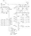
- Fig. 1 is a circuit diagram of a high-frequency switch module 1 according to the first embodiment.
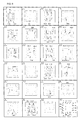
- Fig. 2 is a lamination diagram of a multilayer circuit board in the high-frequency switch module 1.
- the high-frequency switch module 1 has a plurality of external-connection electrodes P M with which the high-frequency switch module 1 is mounted on a circuit board for a circuit at the subsequent stage.
- the external-connection electrode P M of the high-frequency switch module 1 is referred to as an "electrode”
- a mount electrode P IC of the switch IC 10 to be described later is referred to as a "port.”
- the external-connection electrodes P M include an external antenna electrode P M (ANT0), external transmission electrodes P M (TxLB) and P M (TxHB), external reception electrodes P M (Rx1), P M (Rx2), P M (Rx3), and P M (Rx4), external transmission/reception electrodes P M (UM1), P M (UM2), and P M (UM3), an external drive voltage input electrode P M (Vd) for inputting a drive voltage, and external control voltage input electrodes P M (Vc1), P M (Vc2), P M (Vc3), and P M (Vc4) for inputting a control voltage signal.
- the external-connection electrodes P M also include a ground electrode.
- An antenna port P IC (ANT0) of the switch IC 10 having a CMOS structure is connected via an impedance matching circuit 20 to the external antenna electrode P M (ANT0) of the high-frequency switch module 1 connected to an antenna ANT.
- a low-pass filter 200L and a high-pass filter 200H are connected in series between the external antenna electrode P M (ANT0) and the antenna port P IC (ANT0.)
- the low-pass filter 200L is connected to the external antenna electrode P M (ANT0)
- the high-pass filter 200H is connected to the antenna port P IC (ANT0.)
- the low-pass filter 200L includes the inductor Lm2 and a capacitor AC.
- One end of the inductor Lm2 is connected to the external antenna electrode P M (ANT0), and the other end of the inductor Lm2 is connected to the capacitor Cm1 in the high-pass filter 200H.
- One end of the capacitor AC is connected to the external antenna electrode P M (ANT0), and the other end of the capacitor AC is connected to the ground.
- the high-pass filter 200H includes the capacitor Cm1 and the inductor Lm1 (corresponding to a first inductor according to an embodiment of the present invention.) One end of the capacitor Cm1 is connected to the inductor Lm2 in the low-pass filter 200L, and the other end of the capacitor Cm1 is connected to the antenna port P IC (ANT0) of the switch IC 10. One end of the inductor Lm1 is connected to the antenna port P IC (ANT0), and the other end of the inductor Lm1 is connected to the ground.
- the impedance matching circuit 20 functions as a band-pass filter composed of the low-pass filter 200L and the high-pass filter 200H by appropriately setting the inductances of the inductors Lm1 and Lm2 and the capacitances of the capacitors Cm1 and AC. As compared with a case in which only a low-pass or high-pass filter is used, impedance matching can be performed in a wider frequency band. For example, when only a low-pass filter is used, impedance matching is performed in only frequency bands for GSM (global system for mobile communications)-850 and GSM-900. When only a high-pass filter is used, impedance matching is performed in only frequency bands for GSM-1800 and GSM-1900.
- GSM global system for mobile communications
- a high-frequency switch module which is capable of switching signals in four frequency bands or more to be transmitted/received to/from a single antenna and achieving excellent transmission characteristics in all of the frequency bands can be obtained.
- the impedance matching circuit 20 also functions as an ESD protection device and can prevent the switch IC 10 from being destroyed by static electricity.
- a switching speed is approximately 81.6 ⁇ sec.
- a switching speed is approximately 1.2 ⁇ sec.
- the impedance matching circuit 20 when used, it is possible to achieve impedance matching between a switch IC and an antenna in a wide frequency band, ESD protection, and a high-speed switching in the switch IC with a simple configuration.
- the switch IC 10 has, for example, a CMOS structure, and is an SP9T-type FET switch IC that is substantially rectangular in plan view.
- the switch IC 10 is driven by a drive voltage Vdd, and has a function of selectively connecting the antenna port P IC (ANT0) corresponding to a common terminal according to an embodiment of the present invention to one of communication ports P IC (RF1) to P IC (RF9) corresponding to high-frequency signal input/output terminals according to an embodiment of the present invention in accordance with the combination of control voltage signals Vc1 to Vc4.
- an SP9T-type switch IC is used.
- an SPnT-type (n represents a positive number equal to or larger than two) may be used.
- the communication port P IC (RF1) of the switch IC 10 is connected to the external transmission electrode P M (TxLB) via a low-pass filter 30A in the high-frequency switch module 1.
- the low-pass filter 30A includes inductors GLt1 and GLt2 and capacitors GCu1, GCu2, GCu3, GCc1, and GCc2.
- the inductors GLt1 and GLt2 are connected in series between the external transmission electrode P M (TxLB) and the communication port P IC (RF1.)
- the capacitor GCc1 is connected in parallel to the inductor GLt1, and the capacitor GCc2 is connected in parallel to the inductor GLt2.
- the capacitor GCu1 is connected between one end of the inductor GLt1 on the side of the communication port P IC (RF1) and the ground.
- the capacitor GCu2 is connected between a node between the inductors GLt1 and GLt2 and the ground.
- the capacitor GCu3 is connected between one end of the inductor GLt2 on the side of the external transmission electrode P M (TxLB) and the ground.
- the element values of the inductors and the capacitors included in the low-pass filter 30A are set so that the frequency band of a transmission signal input from the external transmission electrode P M (TxLB) becomes a passband and a higher-order harmonic of the transmission signal is attenuated.
- the element values of the inductors and the capacitors included in the low-pass filter 30A are set so that the frequency band of a GSM-850 or GSM-900 transmission signal becomes a passband and the frequency band of a double or triple harmonic of the GSM-850 or GSM-900 transmission signal becomes an attenuation band.
- the communication port P IC (RF2) of the switch IC 10 is connected to the external transmission electrode P M (TxHB) via a low-pass filter 30B in the high-frequency switch module 1.
- the low-pass filter 30B includes inductors DLt1 and DLt2 and capacitors DCu2, DCu3, and DCc1.
- the inductors DLt1 and DLt2 are connected in series between the external transmission electrode P M (TxHB) and the communication port P IC (RF2.)
- the capacitor DCc1 is connected in parallel to the inductor DLt1.
- the capacitor DCu2 is connected between a node between the inductors DLt1 and DLt2 and the ground.
- the capacitor DCu3 is connected between one end of the inductor DLt2 on the side of the external transmission electrode P M (TxHB) and the ground.
- the element values of the inductors and the capacitors included in the low-pass filter 30B are set so that the frequency band of a transmission signal input from the external transmission electrode P M (TxHB) becomes a passband and a higher-order harmonic of the transmission signal is attenuated.
- the element values of the inductors and the capacitors included in the low-pass filter 30B are set so that the frequency band of a GSM-1800 or GSM-1900 transmission signal becomes a passband and the frequency band of a double or triple harmonic of the GSM-1800 or GSM-1900 transmission signal becomes an attenuation band.
- the communication port P IC (RF3) of the switch IC 10 is connected to the external reception electrode P M (Rx1) via the SAW filter SAW1 in the high-frequency switch module 1.
- the SAW filter SAW1 is a filter having a first reception frequency band as a passband.
- the frequency band of a GSM-850 reception signal is set as a passband of the SAW filter SAW1.
- the communication port P IC (RF4) of the switch IC 10 is connected to the external reception electrode P M (Rx2) via the SAW filter SAW2 in the high-frequency switch module 1.
- the SAW filter SAW2 is a filter having a second reception frequency band as a passband.
- the frequency band of a GSM-900 reception signal is set as a passband of the SAW filter SAW2.
- the communication port P IC (RF5) of the switch IC 10 is connected to the external reception electrode P M (Rx3) via the SAW filter SAW3 in the high-frequency switch module 1.
- the SAW filter SAW3 is a filter having a third reception frequency band as a passband.
- the frequency band of a GSM-1800 reception signal is set as a passband of the SAW filter SAW3.
- the communication port P IC (RF5) of the switch IC 10 is connected to the ground by the inductor Lm3 (corresponding to a second inductor according to an embodiment of the present invention.) Since the communication port P IC (RF5) is directly connected to the ground by the inductor Lm3, the inductor Lm3 can quickly discharge static electricity charged in the switch IC 10 to the ground at the time of switching like the inductor Lm1 disposed on the side of the antenna port P IC (ANT0.) As a result, higher-speed switching can be achieved.
- the communication port P IC (RF6) of the switch IC 10 is connected to the external reception electrode P M (Rx4) via the SAW filter SAW4 in the high-frequency switch module 1.
- the SAW filter SAW4 is a filter having a fourth reception frequency band as a passband.
- the frequency band of a GSM-1900 reception signal is set as a passband of the SAW filter SAW4.
- the communication port P IC (RF6) of the switch IC 10 is connected to the ground by the inductor Lm4 (corresponding to the second inductor according to an embodiment of the present invention.) Since the communication port P IC (RF6) is directly connected to the ground by the inductor Lm4, the inductor Lm4 can quickly discharge static electricity charged in the switch IC 10 to the ground at the time of switching like the inductor Lm1 disposed on the side of the antenna port P IC (ANT0) and the inductor Lm3 connected to the communication port P IC (RF5.) As a result, higher-speed switching can be achieved.
- the communication ports P IC (RF7), P IC (RF8), and P IC (RF9) of the switch IC 10 are connected to the external transmission/reception electrodes P M (UM1), P M (UM2), and P M (UM3), respectively, in the high-frequency switch module 1.
- the drive voltage input port P IC (Vd) of the switch IC 10 is connected to the external drive voltage input electrode P M (Vd) via the inductor Ld that is a choke coil in the high-frequency switch module 1.
- the control voltage input ports P IC (Vc1), P IC (Vc2), P IC (Vc3), and P IC (Vc4) of the switch IC 10 are connected to the external control voltage input electrodes P M (Vc1), P M (Vc2), P M (Vc3), and P M (Vc4), respectively, in the high-frequency switch module 1.
- the low-pass filters 30A and 30B are formed by internal electrode patterns.
- Other circuit elements mounted on the surface of the multilayer circuit board and a circuit pattern for connecting each of the external-connection electrodes P M of the high-frequency switch module 1 and corresponding one of the ports P IC of the switch IC 10 are formed by an internal electrode pattern and electrodes on the top and bottom surfaces of the multilayer circuit board.
- the multilayer circuit board is formed by laminating 21 dielectric layers.
- Fig. 2 is a lamination diagram of a multilayer circuit board formed by laminating 21 layers from a 1st layer at the top surface to a 21st layer at the bottom surface in ascending numeric order. Descriptions will be made below with these layer numbers.
- circles in each layer represent conductive via holes. With these via holes, electric connection between electrodes in layers arranged in a lamination direction is established.
- mount lands for the switch IC 10 On the top surface of the 1st layer corresponding to the top surface of the multilayer circuit board, a group of mount lands for the switch IC 10, the inductors Lm1, Lm2, Lm3, Lm4, and Ld, the capacitor Cm1, and the SAW filters SAW1, SAW2, SAW3, and SAW4, which are mount components, is formed. These mount components are mounted so that a predetermined positional relationship among them is satisfied.
- the inductors Lm1, Lm3, and Lm4 are mount components having a higher resistance to a current than that of inductors formed by electrode patterns in the multilayer circuit board and the element values of the inductors Lm1, Lm3, and Lm4 can be more easily selected, it is possible to improve the degree of freedom of selecting an inductor through which a current generated by electrostatic discharging at the time of switching passes.
- the inductors Lm3 and Lm4 are disposed apart from the inductor Lm1, and other elements are disposed between the inductor Lm1 and each of the inductors Lm3 and Lm4.
- the inductors Lm3 and Lm4 are similarly disposed apart from the inductor Lm2, and other elements are similarly disposed between the inductor Lm2 and each of the inductors Lm3 and Lm4.
- the inductors Lm1 and Lm2 disposed on the side of the antenna port of the switch IC 10 are not electromagnetically coupled to the inductors Lm3 and Lm4 disposed on the side of the communication ports of the switch IC 10. This leads to a greater degree of isolation between an antenna port side of the switch IC 10 and a communication port side of the switch IC 10.
- the inductors Lm1 and Lm2 apart from each other and disposing other elements between them, the electromagnetic field coupling between the inductors Lm1 and Lm2 can be prevented. Accordingly, even if a current passes through the inductor Lm1 at the time of switching, mutual induction does not occur at the inductor Lm2. This can prevent the occurrence of noise in the impedance matching circuit 20.
- a ground electrode GND is formed in the 6th layer.
- lead electrode patterns are formed in the 7th layer.
- the ground electrode GND is formed on a substantially entire surface of the 8th layer.
- the ground electrode GND formed in the 8th layer also functions as a counter electrode of the capacitors GCu1 and GCu3.
- electrode patterns forming the inductors GLt1, GLt2, DLt1, and DLt2 are formed.
- electrode patterns forming the inductors GLt1 and GLt2 are formed.
- counter electrodes of the capacitors GCc1, GCc2, and DCc1 and the ground electrode GND are formed.
- the ground electrode GND formed in the 18th layer also functions as a counter electrode of the capacitor AC.
- counter electrodes of the capacitors GCu2, GCu3, DCu2, DCu3, and AC are formed.
- the counter electrode of the capacitor GCu2 also functions as a counter electrode of the capacitors GCc1 and GCc2.
- the counter electrode of the DCu2 also functions as a counter electrode of the capacitor DCc1.
- the ground electrode GND is formed on a substantially entire surface of the 20th layer.
- the ground electrode GND formed in the 20th layer also functions as a counter electrode of the capacitors GCu2, DCu2, DCu3, and AC.
- the coupling between the capacitor AC and another element can be prevented.
- the isolation between the capacitor AC and each circuit pattern on the side of the communication ports of the switch IC 10 formed in the multilayer circuit board can be established. It is therefore possible to prevent noise transmitted from an antenna to an impedance matching circuit to leak into each circuit on the side of the communication ports of the switch IC 10 formed in the multilayer circuit board.
- the external-connection electrodes P M are formed along sides of the bottom surface of the 21st layer corresponding to the bottom surface of the multilayer circuit board. At the center of the layout pattern of the external-connection electrodes P M , the ground electrode GND is formed.
- the external antenna electrode P M (ANT0) is disposed along a side and the external reception electrodes P M (Rx1), P M (Rx2), P M (Rx3), and P M (Rx4) are disposed along an opposite side, so that isolation between the external antenna electrode P M (ANT0) and each of the external reception electrodes P M (Rx1), P M (Rx2), P M (Rx3), and P M (Rx4) is established. Since electrodes adjacent to the external antenna electrode P M (ANT0) disposed along a side are the ground electrodes GND, isolation between the external antenna electrode P M (ANT0) and each external-connection electrode P M is established.
- a high-frequency switch module having the above-described configuration has an excellent transmission characteristic and an ESD protection function and can achieve a high switching speed and size reduction.
- Fig. 3 is a circuit diagram of a high-frequency switch module 1A according to the second embodiment.
- Fig. 4 is a lamination diagram of a multilayer circuit board in the high-frequency switch module 1A.
- a multilayer circuit board in the high-frequency switch module 1A is formed by a stack of a plurality of dielectric layers made of ceramic or a resin. Circuit patterns other than a switch IC 10A, the inductor Lm1, and SAW filters SAW12 and SAW34 in the high-frequency switch module 1A illustrated in Fig. 3 are created by forming electrodes of predetermined patterns in inner layers between the dielectric layers and the top and bottom surfaces of the stack.
- the high-frequency switch module 1A has a plurality of external-connection electrodes P M .
- the external-connection electrodes P M include the external antenna electrode P M (ANT0), the external transmission electrodes P M (TxLB) and P M (TxHB) the external reception electrodes P M (Rx1), P M (Rx2), P M (Rx3), and P M (Rx4), the external transmission/reception electrodes P M (UM1) and P M (UM2), the external drive voltage input electrode P M (Vd) for inputting a drive voltage, and the external control voltage input electrodes P M (Vc1), P M (Vc2), and P M (Vc3) for inputting a control voltage signal.
- the external-connection electrodes P M also include a ground electrode.
- Each of the external reception electrodes P M (Rx1), P M (Rx2), P M (Rx3), and P M (Rx4) is formed by a balanced electrode composed of a pair of electrodes.
- the antenna port P IC (ANT0) of the switch IC 10A is connected via an impedance matching circuit 20A to the external antenna electrode P M (ANT0) connected to the antenna ANT in the high-frequency switch module 1A.
- the impedance matching circuit 20A includes the inductors Lm1 and Lm2 and the capacitor AC.
- the inductor Lm2 is connected in series between the external antenna electrode P M (ANT0) and the antenna port P IC (ANT0.)
- One end of the inductor Lm1 is connected to the antenna port P IC (ANT0), and the other end of the inductor Lm1 is connected to the ground.
- One end of the capacitor AC is connected to the external antenna electrode P M (ANT0), and the other end of the capacitor AC is connected to the ground.
- the impedance matching circuit 20A having the above-described configuration can obtain an operational effect similar to that obtained by the impedance matching circuit 20 according to the first embodiment.
- the switch IC 10A has, for example, a CMOS structure, and is an SP6T-type FET switch IC that is substantially rectangular in plan view.
- the switch IC 10A is driven by the drive voltage Vdd, and has a function of selectively connecting the antenna port P IC (ANT0) corresponding to a common terminal according to an embodiment of the present invention to one of the communication ports P IC (RF1) to P IC (RF6) corresponding to high-frequency signal input/output terminals according to an embodiment of the present invention in accordance with the combination of the control voltage signals Vc1 to Vc3.
- the transmission circuit configuration of the high-frequency switch module 1A is the same as that of the high-frequency switch module 1 according to the first embodiment except for that the capacitor GCu3 is not included in the low-pass filter 30A, and the description given in the first embodiment will be therefore omitted.
- the communication port P IC (RF3) of the switch IC 10A is connected to the external reception electrodes P M (Rx1) and P M (Rx2) via the SAW filter SAW12 in the high-frequency switch module 1A.
- the SAW filter SAW12 is a filter having the first and second reception frequency bands as a passband. For example, the frequency bands of a GSM-850 reception signal and a GSM-900 reception signal are set as a passband of the SAW filter SAW12.
- the connection of the SAW filter SAW12 is performed so that a signal in the first reception frequency band (a GSM-850 reception signal) is output to the external reception electrode P M (Rx1) and a signal in the second reception frequency band (a GSM-900 reception signal) is output to the external reception electrode P M (Rx2.)
- the communication port P IC (RF3) of the switch IC 10A is also connected to the ground by the inductor Lm3.
- the communication port P IC (RF4) of the switch IC 10A is connected to the external reception electrodes P M (Rx3) and P M (Rx4) via the SAW filter SAW34 in the high-frequency switch module 1A.
- the SAW filter SAW34 is a filter having the third and fourth reception frequency bands as a passband. For example, the frequency bands of a GSM-1800 reception signal and a GSM-1900 reception signal are set as a passband of the SAW filter SAW34.
- connection of the SAW filter SAW34 is performed so that a signal in the third reception frequency band (a GSM-1800 reception signal) is output to the external reception electrode P M (Rx3) and a signal in the fourth reception frequency band (a GSM-1900 reception signal) is output to the external reception electrode P M (Rx4.)
- the communication port P IC (RF4) of the switch IC 10A is also connected to the ground by the inductor Lm4.
- the high-frequency switch module 1A having the above-described reception configuration can obtain an operational effect similar to that obtained by the high-frequency switch module 1 according to the first embodiment.
- the communication ports P IC (RF5) and P IC (RF6) of the switch IC 10A are connected to the external transmission/reception electrodes P M (UM1) and P M (UM2), respectively, in the high-frequency switch module 1A.
- the drive voltage input port P IC (Vd) of the switch IC 10A is connected to the external drive voltage input electrode P M (Vd) in the high-frequency switch module 1A.
- the control voltage input ports P IC (Vc1), P IC (Vc2), and P IC (Vc3) of the switch IC 10A are connected to the external control voltage input electrodes P M (Vc1), P M (Vc2), and P M (Vc3), respectively, in the high-frequency switch module 1A.
- the low-pass filters 30A and 30B, the inductor Lm2 and the capacitor AC which are included in the impedance matching circuit 20A, and the inductors Lm3 and Lm4 are formed by internal electrode patterns.
- Other circuit elements are formed by other circuit elements mounted on the surface of the multilayer circuit board.
- a circuit pattern for connecting these circuit elements and a circuit pattern for connecting each of the external-connection electrodes P M of the high-frequency switch module 1A and corresponding one of the ports P IC of the switch IC 10A are formed by an internal electrode pattern and electrodes on the top and bottom surfaces of the multilayer circuit board.
- the multilayer circuit board is formed by laminating 17 dielectric layers.
- Fig. 4 is a lamination diagram of a multilayer circuit board formed by laminating 17 layers from a 1st layer at the top surface to a 17th layer at the bottom surface in ascending numeric order. Descriptions will be made below with these layer numbers.
- circles in each layer represent conductive via holes. With these via holes, electric connection between electrodes in layers arranged in a lamination direction is established.
- mount lands for the switch IC 10A, the inductor Lm1, and the SAW filters SAW12 and SAW34, which are mount components, are mount components. These mount components are mounted so that a predetermined positional relationship among them is satisfied.
- the ground electrode GND is formed on a substantially entire surface of the 4th layer.
- the ground electrode GND formed in the 4th layer also functions as a counter electrode of the capacitor GCu1.
- the counter electrode of the capacitor GCu1 is formed. In the 6th layer, only via holes are formed.
- electrode patterns forming the inductors GLt1, GLt2, DLt1, DLt2, Lm2, Lm3, and Lm4 are formed.
- electrode patterns forming the inductors GLt1, GLt2, Lm2, Lm3, and Lm4 are formed.
- the ground electrode GND is formed in the 13th layer.
- the ground electrode GND formed in the 13th layer also functions as a counter electrode of the capacitor AC.
- the ground electrode GND formed in the 13th layer is formed so that it overlaps the inductor Lm2 in a plan view of the multilayer circuit board (as viewed along the lamination direction.) As a result, the ground electrode GND and the inductor Lm2 are capacitively coupled to each other to generate a capacitance.
- the generated capacitance can be used for fine control of impedance matching performed by the impedance matching circuit 20A.
- counter electrodes of the capacitors GCu2, DCu2, DCu3, and AC are formed.
- the counter electrode of the capacitor GCu2 also functions as a counter electrode of the capacitors GCc1 and GCc2.
- the counter electrode of the capacitor DCu2 also functions as a counter electrode of the capacitor DCc1.
- Fig. 4 by sandwiching the counter electrode of the capacitor AC in the 15th layer between the ground electrode GND in the 13th layer and the ground electrode GND in the 16th layer in the lamination direction, the coupling between the capacitor AC and another element can be prevented like in the first embodiment.
- the external-connection electrodes P M are formed along sides of the bottom surface of the 17th layer corresponding to the bottom surface of the multilayer circuit board. At the center of the layout pattern of the external-connection electrodes P M , the ground electrodes GND are formed.
- the external antenna electrode P M (ANT0) is disposed along a side and the external reception electrodes P M (Rx1), P M (Rx2), P M (Rx3), and P M (Rx4) are disposed along an opposite side, so that isolation between the external antenna electrode P M (ANT0) and each of the external reception electrodes P M (Rx1), P M (Rx2), P M (Rx3), and P M (Rx4) is established.
- a high-frequency switch module having the above-described configuration has an excellent transmission characteristic and an ESD protection function and can achieve a high switching speed and size reduction.
- Fig. 5 is a circuit diagram of a high-frequency switch module 1B according to the third embodiment.
- Fig. 6 is a lamination diagram of a multilayer circuit board in the high-frequency switch module 1B.
- the configuration of the high-frequency switch module 1B is the same as that of the high-frequency switch module 1 according to the first embodiment except for the configuration of an impedance matching circuit 20B and a reception circuit configuration on the side of the communication ports P IC (RF3) to P IC (RF6) of the switch IC 10, and the description given in the first embodiment will be therefore omitted.
- the circuit configuration of the impedance matching circuit 20B is the same as that of the impedance matching circuit 20A according to the second embodiment, and includes the inductors Lm1 and Lm2 and the capacitor AC.
- the inductor Lm2 is connected in series between the external antenna electrode P M (ANT0) and the antenna port P IC (ANT0.)
- One end of the inductor Lm1 is connected to the antenna port P IC (ANT0), and the other end of the inductor Lm1 is connected to the ground.
- One end of the capacitor AC is connected to the external antenna electrode P M (ANT0), and the other end of the capacitor AC is connected to the ground.
- the impedance matching circuit 20B having the above-described configuration can obtain an operational effect similar to that obtained by the impedance matching circuit 20 according to the first embodiment and the impedance matching circuit 20A according to the second embodiment.
- the communication ports P IC (RF3), P IC (RF4), P IC (RF5), and P IC (RF6) of the switch IC 10 are directly connected to the external reception electrodes P M (Rx1), P M (Rx2), P M (Rx3), and P M (Rx4), respectively, in the high-frequency switch module 1B.
- the size of a high-frequency switch module can be further reduced.
- a designer of a circuit board of an electronic apparatus including the high-frequency switch module 1B can freely design a reception circuit configuration.
- the low-pass filters 30A and 30B and the capacitor AC included in the impedance matching circuit 20B are formed by internal electrode patterns.
- Other circuit elements are formed by other circuit elements mounted on the surface of the multilayer circuit board.
- a circuit pattern for connecting these circuit elements and a circuit pattern for connecting each of the external-connection electrodes P M of the high-frequency switch module 1B and corresponding one of the ports P IC of the switch IC 10 are formed by an internal electrode pattern and electrodes on the top and bottom surfaces of the multilayer circuit board.
- the multilayer circuit board is formed by laminating 24 dielectric layers.
- Fig. 6 is a lamination diagram of a multilayer circuit board formed by laminating 24 layers from a 1st layer at the top surface to a 24th layer at the bottom surface in ascending numeric order. Descriptions will be made below with these layer numbers.
- circles in each layer represent conductive via holes. With these via holes, electric connection between electrodes in layers arranged in a lamination direction is established.
- mount lands for the switch IC 10 and the inductors Lm1 and Lm2, which are mount components, is formed on the top surface of the 1st layer corresponding to the top surface of the multilayer circuit board. These mount components are mounted so that a predetermined positional relationship among them is satisfied.
- the ground electrode GND is formed.
- the ground electrode GND formed in the 6th layer also functions as a counter electrode of the capacitor AC.
- the counter electrode of the capacitor AC is formed so that it overlaps the ground electrode GND formed in the 6th layer in a plan view of the multilayer circuit board.
- the ground electrode GND is formed on a substantially entire surface of the 8th layer so that the ground electrode GND covers an area of the 7th layer in which the counter electrode of the capacitor AC is formed.
- the ground electrode GND in the 8th layer functions not only as the counter electrode of the capacitor AC but also as a counter electrode of the capacitors GCu1, GCu3, and DCu1 in relation to the 9th layer.
- the coupling between the capacitor AC and another element can be prevented like in the first and second embodiments. Furthermore, in this embodiment, since only the counter electrode of the capacitor AC is formed in the 7th layer, the coupling between the capacitor AC and another element in the 7th layer can also be prevented.
- electrode patterns forming the inductors GLt1, GLt2, DLt1, and DLt2 are formed.
- an electrode pattern forming the inductor DLt2 is formed.
- only via holes are formed.
- counter electrodes of the capacitors GCc1 and GCc2 are formed in the 20th layer.
- counter electrodes of the capacitors GCu2 and DCu2 are formed in the 21st layer.
- the counter electrode of the capacitor GCu2 formed in the 21st layer also functions as a counter electrode of the capacitors GCc1 and GCc2.
- the counter electrode of the capacitor DCu2 formed in the 21st layer also functions as a counter electrode of the capacitor DCc1.
- the ground electrode GND is formed in the 22nd layer.
- the ground electrode GND formed in the 22nd layer also functions as a counter electrode of the capacitors GCu2 and DCu2.
- the ground electrode GND is formed on a substantially entire surface of the 23rd layer in a plan view of the multilayer circuit board (as viewed along the lamination direction.)
- the external-connection electrodes P M are formed along sides of the bottom surface of the 24th layer corresponding to the bottom surface of the multilayer circuit board. At the center of the layout pattern of the external-connection electrodes P M , the ground electrode GND is formed.
- Fig. 7 is a circuit diagram of a high-frequency switch module 1C according to the fourth embodiment.
- the configuration of the high-frequency switch module 1C is the same as that of the high-frequency switch module 1 according to the first embodiment except for the circuit configuration of an impedance matching circuit 20C. Accordingly, only the impedance matching circuit 20C will be described below.
- the impedance matching circuit 20C includes the inductors Lm1 and Lm2 and the capacitors Cm1 and AC.
- the capacitor Cm1 and the inductor Lm2 are connected in series between the external antenna electrode P M (ANT0) and the antenna port P IC (ANT0.)
- the capacitor Cm1 and the inductor Lm2 are arranged so that the inductor Lm2 is connected to the antenna port P IC (ANT0), that is, the switch IC 10.
- One end of the inductor Lm1 is connected to a node between the inductor Lm2 and the capacitor Cm1, and the other end of the inductor Lm1 is connected to the ground.
- One end of the capacitor AC is connected to the external antenna electrode P M (ANT0), and the other end of the capacitor AC is connected to the ground.
- the antenna port P IC (ANT0) of the switch IC 10 is connected to the ground via the series circuit of the inductors Lm1 and Lm2, that is, via only inductors.
- the impedance matching circuit 20C can obtain an operational effect similar to that obtained by the impedance matching circuit 20 according to the first embodiment and the impedance matching circuit 20A according to the second embodiment.
- any high-frequency switch module having a circuit configuration in which the antenna port P IC (ANT0) of a switch IC is connected to the ground via only an inductor included in an impedance matching circuit connected to the antenna port P IC (ANT0) of the switch IC.
Landscapes
- Engineering & Computer Science (AREA)
- Computer Networks & Wireless Communication (AREA)
- Signal Processing (AREA)
- Transceivers (AREA)
- Electronic Switches (AREA)
Applications Claiming Priority (1)
| Application Number | Priority Date | Filing Date | Title |
|---|---|---|---|
| JP2009225537A JP5136532B2 (ja) | 2009-09-29 | 2009-09-29 | 高周波スイッチモジュール |
Publications (3)
| Publication Number | Publication Date |
|---|---|
| EP2302814A2 true EP2302814A2 (de) | 2011-03-30 |
| EP2302814A3 EP2302814A3 (de) | 2012-08-15 |
| EP2302814B1 EP2302814B1 (de) | 2018-08-01 |
Family
ID=43414181
Family Applications (1)
| Application Number | Title | Priority Date | Filing Date |
|---|---|---|---|
| EP10174201.3A Active EP2302814B1 (de) | 2009-09-29 | 2010-08-26 | Hochfrequenzschaltmodul |
Country Status (3)
| Country | Link |
|---|---|
| US (1) | US8466733B2 (de) |
| EP (1) | EP2302814B1 (de) |
| JP (1) | JP5136532B2 (de) |
Cited By (1)
| Publication number | Priority date | Publication date | Assignee | Title |
|---|---|---|---|---|
| US8831535B2 (en) | 2011-02-14 | 2014-09-09 | Murata Manufacturing Co., Ltd. | High-frequency module |
Families Citing this family (18)
| Publication number | Priority date | Publication date | Assignee | Title |
|---|---|---|---|---|
| GB201102143D0 (en) * | 2011-02-08 | 2011-03-23 | Cambridge Silicon Radio Ltd | A receiver |
| CN103828249B (zh) * | 2011-09-26 | 2016-08-17 | 株式会社村田制作所 | 高频模块 |
| CN102420634A (zh) * | 2011-12-07 | 2012-04-18 | 捷开通讯科技(上海)有限公司 | 无线通信收发系统 |
| JP5610099B2 (ja) * | 2012-02-21 | 2014-10-22 | 株式会社村田製作所 | 高周波スイッチモジュール |
| JP5783186B2 (ja) | 2013-01-21 | 2015-09-24 | 株式会社村田製作所 | 積層基板モジュール |
| JP5751265B2 (ja) | 2013-02-06 | 2015-07-22 | 株式会社村田製作所 | 高周波モジュール |
| WO2014129015A1 (ja) * | 2013-02-22 | 2014-08-28 | 株式会社村田製作所 | 高周波モジュール |
| JP6183461B2 (ja) | 2013-08-06 | 2017-08-23 | 株式会社村田製作所 | 高周波モジュール |
| JP6571381B2 (ja) * | 2014-05-12 | 2019-09-04 | ローム株式会社 | 無線通信モジュール |
| JP6278925B2 (ja) * | 2015-04-24 | 2018-02-14 | 三菱電機株式会社 | マルチポートスイッチ |
| CN107615669B (zh) | 2015-06-03 | 2020-04-07 | 株式会社村田制作所 | 高频前置电路 |
| KR101971901B1 (ko) | 2015-06-03 | 2019-04-24 | 가부시키가이샤 무라타 세이사쿠쇼 | 고주파 프론트 엔드 회로 |
| JP6222406B2 (ja) * | 2015-06-24 | 2017-11-01 | 株式会社村田製作所 | マルチプレクサ、送信装置、受信装置、高周波フロントエンド回路、通信装置、およびマルチプレクサのインピーダンス整合方法 |
| WO2017135408A1 (ja) * | 2016-02-05 | 2017-08-10 | 株式会社村田製作所 | 高周波モジュール |
| US10742026B2 (en) * | 2018-02-07 | 2020-08-11 | International Business Machines Corporation | Electrostatic protection device |
| JP2020088643A (ja) * | 2018-11-27 | 2020-06-04 | 住友電気工業株式会社 | 単極双投スイッチ |
| US12580597B2 (en) * | 2022-03-10 | 2026-03-17 | Samsung Electronics Co., Ltd. | CMOS chip and electronic device including the CMOS chip |
| JP2024150355A (ja) * | 2023-04-10 | 2024-10-23 | 株式会社村田製作所 | 高周波モジュール及び通信装置 |
Citations (1)
| Publication number | Priority date | Publication date | Assignee | Title |
|---|---|---|---|---|
| JP2005505186A (ja) | 2001-09-28 | 2005-02-17 | エプコス アクチエンゲゼルシャフト | 回路装置、該回路装置を有するスイッチングモジュール、および該スイッチングモジュールの使用方法 |
Family Cites Families (15)
| Publication number | Priority date | Publication date | Assignee | Title |
|---|---|---|---|---|
| JP2978553B2 (ja) * | 1990-10-29 | 1999-11-15 | ティーディーケイ株式会社 | コンデンサブロック |
| JP3487692B2 (ja) * | 1995-10-02 | 2004-01-19 | 富士通株式会社 | 分波器 |
| JPH09181641A (ja) | 1995-12-22 | 1997-07-11 | Sharp Corp | 高周波スイッチ |
| JP2001189677A (ja) * | 1999-12-28 | 2001-07-10 | Murata Mfg Co Ltd | 高周波回路部品および通信装置 |
| JP4224802B2 (ja) | 2002-03-18 | 2009-02-18 | 日立金属株式会社 | ハイパスフィルタおよびこれを用いたマルチバンドアンテナスイッチ回路、マルチバンドアンテナスイッチ積層モジュール並びに通信装置 |
| US7057472B2 (en) | 2001-08-10 | 2006-06-06 | Hitachi Metals, Ltd. | Bypass filter, multi-band antenna switch circuit, and layered module composite part and communication device using them |
| JP2003124702A (ja) * | 2001-10-12 | 2003-04-25 | Murata Mfg Co Ltd | 高周波複合部品 |
| JP2004253953A (ja) * | 2003-02-19 | 2004-09-09 | Hitachi Metals Ltd | アンテナスイッチ回路及びこれを用いたアンテナスイッチモジュール並びに通信装置 |
| DE102004016399B4 (de) * | 2003-03-27 | 2013-06-06 | Kyocera Corp. | Hochfrequenzmodul und Funkvorrichtung |
| JP4123435B2 (ja) * | 2003-10-14 | 2008-07-23 | 富士通メディアデバイス株式会社 | 高周波スイッチモジュール |
| JP4775686B2 (ja) * | 2004-02-24 | 2011-09-21 | 日立金属株式会社 | 積層ローパスフィルタ及びそれを用いた高周波スイッチモジュール |
| ATE434291T1 (de) | 2004-03-30 | 2009-07-15 | Tdk Corp | Diplexer- und anpass-schaltung |
| MX2007005483A (es) * | 2004-11-05 | 2007-07-16 | Qualcomm Inc | Transceptor agil de frecuencia para uso en un dispositivo de comunicaciones manual de banda multiple. |
| US20070085754A1 (en) * | 2005-10-18 | 2007-04-19 | Nokia Corporation | RF front-end architecture for a separate non-50 ohm antenna system |
| TW200924276A (en) * | 2007-11-28 | 2009-06-01 | Murata Manufacturing Co | Low-voltage control high-frequency switch and composite high frequency component |
-
2009
- 2009-09-29 JP JP2009225537A patent/JP5136532B2/ja active Active
-
2010
- 2010-08-26 EP EP10174201.3A patent/EP2302814B1/de active Active
- 2010-09-24 US US12/889,456 patent/US8466733B2/en active Active
Patent Citations (1)
| Publication number | Priority date | Publication date | Assignee | Title |
|---|---|---|---|---|
| JP2005505186A (ja) | 2001-09-28 | 2005-02-17 | エプコス アクチエンゲゼルシャフト | 回路装置、該回路装置を有するスイッチングモジュール、および該スイッチングモジュールの使用方法 |
Cited By (1)
| Publication number | Priority date | Publication date | Assignee | Title |
|---|---|---|---|---|
| US8831535B2 (en) | 2011-02-14 | 2014-09-09 | Murata Manufacturing Co., Ltd. | High-frequency module |
Also Published As
| Publication number | Publication date |
|---|---|
| EP2302814A3 (de) | 2012-08-15 |
| US8466733B2 (en) | 2013-06-18 |
| US20110234295A1 (en) | 2011-09-29 |
| EP2302814B1 (de) | 2018-08-01 |
| JP5136532B2 (ja) | 2013-02-06 |
| JP2011077723A (ja) | 2011-04-14 |
| CN102035522A (zh) | 2011-04-27 |
Similar Documents
| Publication | Publication Date | Title |
|---|---|---|
| EP2302814B1 (de) | Hochfrequenzschaltmodul | |
| EP2662985B1 (de) | Hochfrequenzmodul | |
| US6788958B2 (en) | High-frequency module and mobile communication apparatus using the same | |
| JP5625453B2 (ja) | 高周波スイッチモジュール | |
| US7561005B2 (en) | High frequency front-end module and duplexer | |
| KR20210002684A (ko) | 고주파 모듈 및 통신 장치 | |
| KR20090035480A (ko) | 분기 회로, 고주파 회로 및 고주파 모듈 | |
| US9077439B2 (en) | High-frequency module | |
| KR20210003274A (ko) | 고주파 모듈 및 통신 장치 | |
| EP0909023B1 (de) | In einer Vielzahl von Frequenzbändern arbeitendes Filter | |
| US8467740B2 (en) | High-frequency module | |
| EP2487802B1 (de) | Hochfrequenzmodul | |
| US7711389B2 (en) | High frequency module | |
| US7904031B2 (en) | High-frequency module for transmitting and receiving transmission-reception signals of at least three communication systems using a single antenna | |
| US11075658B2 (en) | Multilayer substrate, filter, multiplexer, radio-frequency front-end circuit, and communication device | |
| CN217957069U (zh) | 收发模块 | |
| CN102187572B (zh) | Lc滤波器及高频开关模块 | |
| JP4775686B2 (ja) | 積層ローパスフィルタ及びそれを用いた高周波スイッチモジュール | |
| JP5790852B2 (ja) | 高周波スイッチモジュール | |
| JP2008048450A (ja) | 高周波モジュール |
Legal Events
| Date | Code | Title | Description |
|---|---|---|---|
| PUAI | Public reference made under article 153(3) epc to a published international application that has entered the european phase |
Free format text: ORIGINAL CODE: 0009012 |
|
| 17P | Request for examination filed |
Effective date: 20100826 |
|
| AK | Designated contracting states |
Kind code of ref document: A2 Designated state(s): AL AT BE BG CH CY CZ DE DK EE ES FI FR GB GR HR HU IE IS IT LI LT LU LV MC MK MT NL NO PL PT RO SE SI SK SM TR |
|
| AX | Request for extension of the european patent |
Extension state: BA ME RS |
|
| RIC1 | Information provided on ipc code assigned before grant |
Ipc: H03H 7/46 20060101ALI20120118BHEP Ipc: H03H 7/40 20060101ALI20120118BHEP Ipc: H03H 7/48 20060101ALI20120118BHEP Ipc: H04B 1/00 20060101ALI20120118BHEP Ipc: H04B 1/04 20060101ALI20120118BHEP Ipc: H03H 7/38 20060101ALI20120118BHEP Ipc: H04B 1/18 20060101AFI20120118BHEP |
|
| PUAL | Search report despatched |
Free format text: ORIGINAL CODE: 0009013 |
|
| AK | Designated contracting states |
Kind code of ref document: A3 Designated state(s): AL AT BE BG CH CY CZ DE DK EE ES FI FR GB GR HR HU IE IS IT LI LT LU LV MC MK MT NL NO PL PT RO SE SI SK SM TR |
|
| AX | Request for extension of the european patent |
Extension state: BA ME RS |
|
| RIC1 | Information provided on ipc code assigned before grant |
Ipc: H04B 1/18 20060101AFI20120706BHEP Ipc: H03H 7/40 20060101ALI20120706BHEP Ipc: H04B 1/04 20060101ALI20120706BHEP Ipc: H03H 7/48 20060101ALI20120706BHEP Ipc: H03H 7/46 20060101ALI20120706BHEP Ipc: H04B 1/00 20060101ALI20120706BHEP Ipc: H03H 7/38 20060101ALI20120706BHEP |
|
| GRAP | Despatch of communication of intention to grant a patent |
Free format text: ORIGINAL CODE: EPIDOSNIGR1 |
|
| RIC1 | Information provided on ipc code assigned before grant |
Ipc: H03H 7/38 20060101ALI20180115BHEP Ipc: H03H 7/46 20060101ALI20180115BHEP Ipc: H03H 1/00 20060101ALI20180115BHEP Ipc: H03H 7/01 20060101ALI20180115BHEP Ipc: H03H 7/48 20060101ALI20180115BHEP Ipc: H04B 1/18 20060101AFI20180115BHEP Ipc: H04B 1/04 20060101ALI20180115BHEP Ipc: H04B 1/00 20060101ALI20180115BHEP Ipc: H03H 7/40 20060101ALI20180115BHEP |
|
| INTG | Intention to grant announced |
Effective date: 20180212 |
|
| GRAS | Grant fee paid |
Free format text: ORIGINAL CODE: EPIDOSNIGR3 |
|
| GRAA | (expected) grant |
Free format text: ORIGINAL CODE: 0009210 |
|
| AK | Designated contracting states |
Kind code of ref document: B1 Designated state(s): AL AT BE BG CH CY CZ DE DK EE ES FI FR GB GR HR HU IE IS IT LI LT LU LV MC MK MT NL NO PL PT RO SE SI SK SM TR |
|
| REG | Reference to a national code |
Ref country code: GB Ref legal event code: FG4D |
|
| REG | Reference to a national code |
Ref country code: CH Ref legal event code: EP Ref country code: AT Ref legal event code: REF Ref document number: 1025544 Country of ref document: AT Kind code of ref document: T Effective date: 20180815 |
|
| REG | Reference to a national code |
Ref country code: IE Ref legal event code: FG4D |
|
| REG | Reference to a national code |
Ref country code: DE Ref legal event code: R096 Ref document number: 602010052301 Country of ref document: DE |
|
| REG | Reference to a national code |
Ref country code: NL Ref legal event code: MP Effective date: 20180801 |
|
| REG | Reference to a national code |
Ref country code: LT Ref legal event code: MG4D |
|
| REG | Reference to a national code |
Ref country code: AT Ref legal event code: MK05 Ref document number: 1025544 Country of ref document: AT Kind code of ref document: T Effective date: 20180801 |
|
| PG25 | Lapsed in a contracting state [announced via postgrant information from national office to epo] |
Ref country code: SE Free format text: LAPSE BECAUSE OF FAILURE TO SUBMIT A TRANSLATION OF THE DESCRIPTION OR TO PAY THE FEE WITHIN THE PRESCRIBED TIME-LIMIT Effective date: 20180801 Ref country code: BG Free format text: LAPSE BECAUSE OF FAILURE TO SUBMIT A TRANSLATION OF THE DESCRIPTION OR TO PAY THE FEE WITHIN THE PRESCRIBED TIME-LIMIT Effective date: 20181101 Ref country code: NL Free format text: LAPSE BECAUSE OF FAILURE TO SUBMIT A TRANSLATION OF THE DESCRIPTION OR TO PAY THE FEE WITHIN THE PRESCRIBED TIME-LIMIT Effective date: 20180801 Ref country code: NO Free format text: LAPSE BECAUSE OF FAILURE TO SUBMIT A TRANSLATION OF THE DESCRIPTION OR TO PAY THE FEE WITHIN THE PRESCRIBED TIME-LIMIT Effective date: 20181101 Ref country code: GR Free format text: LAPSE BECAUSE OF FAILURE TO SUBMIT A TRANSLATION OF THE DESCRIPTION OR TO PAY THE FEE WITHIN THE PRESCRIBED TIME-LIMIT Effective date: 20181102 Ref country code: LT Free format text: LAPSE BECAUSE OF FAILURE TO SUBMIT A TRANSLATION OF THE DESCRIPTION OR TO PAY THE FEE WITHIN THE PRESCRIBED TIME-LIMIT Effective date: 20180801 Ref country code: IS Free format text: LAPSE BECAUSE OF FAILURE TO SUBMIT A TRANSLATION OF THE DESCRIPTION OR TO PAY THE FEE WITHIN THE PRESCRIBED TIME-LIMIT Effective date: 20181201 Ref country code: AT Free format text: LAPSE BECAUSE OF FAILURE TO SUBMIT A TRANSLATION OF THE DESCRIPTION OR TO PAY THE FEE WITHIN THE PRESCRIBED TIME-LIMIT Effective date: 20180801 Ref country code: FI Free format text: LAPSE BECAUSE OF FAILURE TO SUBMIT A TRANSLATION OF THE DESCRIPTION OR TO PAY THE FEE WITHIN THE PRESCRIBED TIME-LIMIT Effective date: 20180801 Ref country code: PL Free format text: LAPSE BECAUSE OF FAILURE TO SUBMIT A TRANSLATION OF THE DESCRIPTION OR TO PAY THE FEE WITHIN THE PRESCRIBED TIME-LIMIT Effective date: 20180801 |
|
| PG25 | Lapsed in a contracting state [announced via postgrant information from national office to epo] |
Ref country code: LV Free format text: LAPSE BECAUSE OF FAILURE TO SUBMIT A TRANSLATION OF THE DESCRIPTION OR TO PAY THE FEE WITHIN THE PRESCRIBED TIME-LIMIT Effective date: 20180801 Ref country code: AL Free format text: LAPSE BECAUSE OF FAILURE TO SUBMIT A TRANSLATION OF THE DESCRIPTION OR TO PAY THE FEE WITHIN THE PRESCRIBED TIME-LIMIT Effective date: 20180801 Ref country code: HR Free format text: LAPSE BECAUSE OF FAILURE TO SUBMIT A TRANSLATION OF THE DESCRIPTION OR TO PAY THE FEE WITHIN THE PRESCRIBED TIME-LIMIT Effective date: 20180801 Ref country code: ES Free format text: LAPSE BECAUSE OF FAILURE TO SUBMIT A TRANSLATION OF THE DESCRIPTION OR TO PAY THE FEE WITHIN THE PRESCRIBED TIME-LIMIT Effective date: 20180801 |
|
| REG | Reference to a national code |
Ref country code: CH Ref legal event code: PL |
|
| PG25 | Lapsed in a contracting state [announced via postgrant information from national office to epo] |
Ref country code: IT Free format text: LAPSE BECAUSE OF FAILURE TO SUBMIT A TRANSLATION OF THE DESCRIPTION OR TO PAY THE FEE WITHIN THE PRESCRIBED TIME-LIMIT Effective date: 20180801 Ref country code: LI Free format text: LAPSE BECAUSE OF NON-PAYMENT OF DUE FEES Effective date: 20180831 Ref country code: MC Free format text: LAPSE BECAUSE OF FAILURE TO SUBMIT A TRANSLATION OF THE DESCRIPTION OR TO PAY THE FEE WITHIN THE PRESCRIBED TIME-LIMIT Effective date: 20180801 Ref country code: LU Free format text: LAPSE BECAUSE OF NON-PAYMENT OF DUE FEES Effective date: 20180826 Ref country code: CH Free format text: LAPSE BECAUSE OF NON-PAYMENT OF DUE FEES Effective date: 20180831 Ref country code: EE Free format text: LAPSE BECAUSE OF FAILURE TO SUBMIT A TRANSLATION OF THE DESCRIPTION OR TO PAY THE FEE WITHIN THE PRESCRIBED TIME-LIMIT Effective date: 20180801 Ref country code: CZ Free format text: LAPSE BECAUSE OF FAILURE TO SUBMIT A TRANSLATION OF THE DESCRIPTION OR TO PAY THE FEE WITHIN THE PRESCRIBED TIME-LIMIT Effective date: 20180801 Ref country code: RO Free format text: LAPSE BECAUSE OF FAILURE TO SUBMIT A TRANSLATION OF THE DESCRIPTION OR TO PAY THE FEE WITHIN THE PRESCRIBED TIME-LIMIT Effective date: 20180801 |
|
| REG | Reference to a national code |
Ref country code: DE Ref legal event code: R097 Ref document number: 602010052301 Country of ref document: DE |
|
| REG | Reference to a national code |
Ref country code: BE Ref legal event code: MM Effective date: 20180831 |
|
| PG25 | Lapsed in a contracting state [announced via postgrant information from national office to epo] |
Ref country code: SM Free format text: LAPSE BECAUSE OF FAILURE TO SUBMIT A TRANSLATION OF THE DESCRIPTION OR TO PAY THE FEE WITHIN THE PRESCRIBED TIME-LIMIT Effective date: 20180801 Ref country code: DK Free format text: LAPSE BECAUSE OF FAILURE TO SUBMIT A TRANSLATION OF THE DESCRIPTION OR TO PAY THE FEE WITHIN THE PRESCRIBED TIME-LIMIT Effective date: 20180801 Ref country code: SK Free format text: LAPSE BECAUSE OF FAILURE TO SUBMIT A TRANSLATION OF THE DESCRIPTION OR TO PAY THE FEE WITHIN THE PRESCRIBED TIME-LIMIT Effective date: 20180801 |
|
| PLBE | No opposition filed within time limit |
Free format text: ORIGINAL CODE: 0009261 |
|
| STAA | Information on the status of an ep patent application or granted ep patent |
Free format text: STATUS: NO OPPOSITION FILED WITHIN TIME LIMIT |
|
| 26N | No opposition filed |
Effective date: 20190503 |
|
| GBPC | Gb: european patent ceased through non-payment of renewal fee |
Effective date: 20181101 |
|
| PG25 | Lapsed in a contracting state [announced via postgrant information from national office to epo] |
Ref country code: BE Free format text: LAPSE BECAUSE OF NON-PAYMENT OF DUE FEES Effective date: 20180831 Ref country code: FR Free format text: LAPSE BECAUSE OF NON-PAYMENT OF DUE FEES Effective date: 20181001 Ref country code: SI Free format text: LAPSE BECAUSE OF FAILURE TO SUBMIT A TRANSLATION OF THE DESCRIPTION OR TO PAY THE FEE WITHIN THE PRESCRIBED TIME-LIMIT Effective date: 20180801 |
|
| PG25 | Lapsed in a contracting state [announced via postgrant information from national office to epo] |
Ref country code: GB Free format text: LAPSE BECAUSE OF NON-PAYMENT OF DUE FEES Effective date: 20181101 |
|
| PG25 | Lapsed in a contracting state [announced via postgrant information from national office to epo] |
Ref country code: MT Free format text: LAPSE BECAUSE OF NON-PAYMENT OF DUE FEES Effective date: 20180826 |
|
| PG25 | Lapsed in a contracting state [announced via postgrant information from national office to epo] |
Ref country code: TR Free format text: LAPSE BECAUSE OF FAILURE TO SUBMIT A TRANSLATION OF THE DESCRIPTION OR TO PAY THE FEE WITHIN THE PRESCRIBED TIME-LIMIT Effective date: 20180801 |
|
| PG25 | Lapsed in a contracting state [announced via postgrant information from national office to epo] |
Ref country code: HU Free format text: LAPSE BECAUSE OF FAILURE TO SUBMIT A TRANSLATION OF THE DESCRIPTION OR TO PAY THE FEE WITHIN THE PRESCRIBED TIME-LIMIT; INVALID AB INITIO Effective date: 20100826 Ref country code: PT Free format text: LAPSE BECAUSE OF FAILURE TO SUBMIT A TRANSLATION OF THE DESCRIPTION OR TO PAY THE FEE WITHIN THE PRESCRIBED TIME-LIMIT Effective date: 20180801 |
|
| PG25 | Lapsed in a contracting state [announced via postgrant information from national office to epo] |
Ref country code: IE Free format text: LAPSE BECAUSE OF NON-PAYMENT OF DUE FEES Effective date: 20180826 Ref country code: CY Free format text: LAPSE BECAUSE OF FAILURE TO SUBMIT A TRANSLATION OF THE DESCRIPTION OR TO PAY THE FEE WITHIN THE PRESCRIBED TIME-LIMIT Effective date: 20180801 Ref country code: MK Free format text: LAPSE BECAUSE OF NON-PAYMENT OF DUE FEES Effective date: 20180801 |
|
| PGFP | Annual fee paid to national office [announced via postgrant information from national office to epo] |
Ref country code: DE Payment date: 20250820 Year of fee payment: 16 |