EP2316986A1 - System zur chemischen Gasphasenabscheidung - Google Patents
System zur chemischen Gasphasenabscheidung Download PDFInfo
- Publication number
- EP2316986A1 EP2316986A1 EP11152605A EP11152605A EP2316986A1 EP 2316986 A1 EP2316986 A1 EP 2316986A1 EP 11152605 A EP11152605 A EP 11152605A EP 11152605 A EP11152605 A EP 11152605A EP 2316986 A1 EP2316986 A1 EP 2316986A1
- Authority
- EP
- European Patent Office
- Prior art keywords
- seal
- glass sheet
- deposition chamber
- chemical vapor
- sheet substrates
- Prior art date
- Legal status (The legal status is an assumption and is not a legal conclusion. Google has not performed a legal analysis and makes no representation as to the accuracy of the status listed.)
- Granted
Links
Images


Classifications
-
- C—CHEMISTRY; METALLURGY
- C23—COATING METALLIC MATERIAL; COATING MATERIAL WITH METALLIC MATERIAL; CHEMICAL SURFACE TREATMENT; DIFFUSION TREATMENT OF METALLIC MATERIAL; COATING BY VACUUM EVAPORATION, BY SPUTTERING, BY ION IMPLANTATION OR BY CHEMICAL VAPOUR DEPOSITION, IN GENERAL; INHIBITING CORROSION OF METALLIC MATERIAL OR INCRUSTATION IN GENERAL
- C23C—COATING METALLIC MATERIAL; COATING MATERIAL WITH METALLIC MATERIAL; SURFACE TREATMENT OF METALLIC MATERIAL BY DIFFUSION INTO THE SURFACE, BY CHEMICAL CONVERSION OR SUBSTITUTION; COATING BY VACUUM EVAPORATION, BY SPUTTERING, BY ION IMPLANTATION OR BY CHEMICAL VAPOUR DEPOSITION, IN GENERAL
- C23C16/00—Chemical coating by decomposition of gaseous compounds, without leaving reaction products of surface material in the coating, i.e. chemical vapour deposition [CVD] processes
- C23C16/44—Chemical coating by decomposition of gaseous compounds, without leaving reaction products of surface material in the coating, i.e. chemical vapour deposition [CVD] processes characterised by the method of coating
- C23C16/4401—Means for minimising impurities, e.g. dust, moisture or residual gas, in the reaction chamber
- C23C16/4409—Means for minimising impurities, e.g. dust, moisture or residual gas, in the reaction chamber characterised by sealing means
-
- C—CHEMISTRY; METALLURGY
- C03—GLASS; MINERAL OR SLAG WOOL
- C03C—CHEMICAL COMPOSITION OF GLASSES, GLAZES OR VITREOUS ENAMELS; SURFACE TREATMENT OF GLASS; SURFACE TREATMENT OF FIBRES OR FILAMENTS MADE FROM GLASS, MINERALS OR SLAGS; JOINING GLASS TO GLASS OR OTHER MATERIALS
- C03C17/00—Surface treatment of glass, not in the form of fibres or filaments, by coating
- C03C17/001—General methods for coating; Devices therefor
- C03C17/002—General methods for coating; Devices therefor for flat glass, e.g. float glass
-
- C—CHEMISTRY; METALLURGY
- C23—COATING METALLIC MATERIAL; COATING MATERIAL WITH METALLIC MATERIAL; CHEMICAL SURFACE TREATMENT; DIFFUSION TREATMENT OF METALLIC MATERIAL; COATING BY VACUUM EVAPORATION, BY SPUTTERING, BY ION IMPLANTATION OR BY CHEMICAL VAPOUR DEPOSITION, IN GENERAL; INHIBITING CORROSION OF METALLIC MATERIAL OR INCRUSTATION IN GENERAL
- C23C—COATING METALLIC MATERIAL; COATING MATERIAL WITH METALLIC MATERIAL; SURFACE TREATMENT OF METALLIC MATERIAL BY DIFFUSION INTO THE SURFACE, BY CHEMICAL CONVERSION OR SUBSTITUTION; COATING BY VACUUM EVAPORATION, BY SPUTTERING, BY ION IMPLANTATION OR BY CHEMICAL VAPOUR DEPOSITION, IN GENERAL
- C23C16/00—Chemical coating by decomposition of gaseous compounds, without leaving reaction products of surface material in the coating, i.e. chemical vapour deposition [CVD] processes
- C23C16/44—Chemical coating by decomposition of gaseous compounds, without leaving reaction products of surface material in the coating, i.e. chemical vapour deposition [CVD] processes characterised by the method of coating
- C23C16/54—Apparatus specially adapted for continuous coating
Definitions
- This invention relates to a chemical vapor deposition system for depositing coatings on glass sheet substrates.
- Coatings have previously been applied to glass sheet substrates to make semiconductor devices such as photovoltaic panels.
- One way in which such coatings are applied is by chemical vapor deposition. Close-spaced sublimation was previously utilized to apply coatings such as cadmium sulfide and cadmium telluride to a glass sheet substrate by inserting the substrate on a batch basis into a sealed chamber that is then heated.
- the glass sheet substrate in close-spaced sublimation is supported at its periphery in a very close relationship, normally two to three millimeters, to a source of material of cadmium telluride.
- the heating by such a process proceeds to about 450° to 500°C whereupon the cadmium telluride begins to sublime very slowly into elemental components and, upon reaching an temperature of about 650° to 725°C, the sublimation is at a greater rate and the elemental components recombine at a significant rate on the downwardly facing surface of the substrate.
- An object of the present invention is to provide an improved chemical vapor deposition system for providing coatings on glass sheet substrates.
- the chemical vapor deposition system of the invention includes a housing that defines an enclosed deposition chamber and includes a lower portion and an upper portion having a horizontal junction with each other.
- a seal assembly extends between the lower and upper housing portions at their horizontal junction to seal the deposition chamber.
- a roll conveyor located within the deposition chamber conveys glass sheet substrates along a direction of conveyance at a plane of conveyance below the horizontal junction of the lower and upper housing portions where the seal assembly is located.
- a chemical vapor distributor is located within the deposition chamber above the roll conveyor to provide chemical vapor deposition of a coating on the conveyed glass sheet substrates.
- the housing includes an entry through which the glass sheet substrates to be coated are introduced into the deposition chamber at a location below the horizontal junction of the lower and upper housing portion where the seal assembly is located, and the housing also includes an exit through which the coated glass sheet substrates leave the deposition chamber at a location below the horizontal junction of the lower and upper housing portions where the seal assembly is located.
- the deposition system includes a vacuum source for drawing a vacuum within the deposition chamber.
- the seal assembly between the lower and upper housing portions includes inner and outer seal members spaced from each other to define an intermediate seal space that is located between the deposition chamber and the ambient and in which a vacuum is drawn to a lesser extent than in the deposition chamber.
- a sensor detects the pressure within the seal space to sense leakage of either the inner seal member or the outer seal member.
- the seal assembly includes lower and upper seal flanges on the lower and upper housing portions, and the inner and outer seal members extend between the lower and upper seal flanges to seal between the lower and upper housing portions. Clamps extend between the lower and upper seal flanges to secure the upper housing portion to the lower housing portion. Each clamp includes a hydraulic cylinder operable to provide the securement between the lower and upper seal flanges.
- the deposition system includes an oven located within the housing and having elongated heaters that extend along the direction of conveyance in laterally spaced banks to heat the conveyed glass sheet substrates and control temperature differentials of the substrates laterally with respect to the direction of conveyance.
- Each elongated heater includes an electric resistance element through which electricity is passed to provide heating, and each heater includes an elongated quartz tube through which the electric resistance element extends.
- the roll conveyor includes rolls that extend through the oven and have ends projecting outwardly therefrom within the housing, and a drive mechanism engages and rotatively drives the roll ends outwardly of the oven within the housing.
- the deposition system also includes a screen that is located below the roll conveyor to catch any broken glass sheet substrates.
- the screen is made of stainless steel and includes stiffeners.
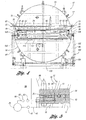
- a chemical vapor deposition system constructed in accordance with the present invention is generally indicated by 10 and includes a housing 12 that defines an enclosed deposition chamber 14 in which chemical vapor deposition takers place as is hereinafter more fully described.
- the housing 12 as shown in Figure 1 includes a lower portion 16 and an upper portion 18 that have a horizontal planar junction 20 with each other.
- a seal assembly 22 extends between the lower and upper housing portions 16 and 18 at their horizontal junction 20 to seal the housing 12. This seal assembly extends along each lateral side of the elongated length of the system housing and along each of its opposite ends so as to extend completely around the housing.
- a roll conveyor 24 is located within the deposition chamber 14 to convey glass sheet substrate G along a direction of conveyance C at a plane of conveyance that is identified by pc in Figure 1 .
- This plane of conveyance pc is located below the horizontal junction 20 of the lower and upper housing portions 16 and 18 where the seal assembly 22 is located.
- a chemical vapor distributor collectively indicated by 26 includes distributor plenums 28 that are located within the deposition chamber 14 above the roll conveyor 24 to provide chemical vapor deposition of a coating on the conveyed glass sheet substrates.
- the distributor plenums 28 are preferably of the type disclosed by United States Patents 5,945,163 Powell et al. and 6,037,241 Powell et al. , the entire disclosures of which are hereby incorporated by reference, wherein the chemical vapor to be deposited is passed through a heated permeable membrane prior to being discharged for flow downwardly toward the roll conveyor onto the adjacent conveyed glass sheet substrate for the deposition.
- the housing includes an entry 30 through which the glass sheet substrates to be coated are introduced into the deposition chamber 14 about a location below the horizontal junction 20 of the lower and upper housing portions 16 and 18 where the seal assembly 22 is located.
- the housing as shown in Figure 1 includes an exit 32 through which the coated glass sheet substrates leave the deposition chamber 14 at a location below the horizontal junction 20 of the lower and upper housing portions 16 and 18 where the seal assembly 22 is located.
- the entry 30 and exit 32 as illustrated by the entry shown in Figure 4 function as open passways between other processing systems.
- the entry 30 can receive heated glass sheets from a heating furnace for the deposition, and the exit 32 can transfer the coated glass sheets for further processing.
- the other system portions will have suitable seals that maintain the contained environment therein as well as within the deposition system 10.
- Such seals can be conventional load lock cells with spaced gates and evacuation pumping apparatus for providing the glass sheet introduction in a conventional manner without any introduction of the environmental atmosphere into the deposition chamber 14.
- the entry 30 and exit 32 can be load lock cells or any type of suitable engagement seals or a slit seal for permitting continuous introduction of glass sheets such as disclosed by United States Patent 5,772,715 McMaster et al. , the entire disclosure of which is hereby incorporated by reference.
- the chemical vapor distributor 26 has a material source 34 that feeds a pair of inlets 36 to opposite lateral sides of the system for flow to the opposite lateral ends of the distributor plenums 28 in order to ensure uniform distribution of the deposition on the glass sheet substrates as they are conveyed along the roll conveyor 24.
- the chemical vapor deposition system 10 includes a vacuum source 38 for drawing a vacuum in the deposition chamber 14 through a conduit 40 under the control of a valve 42.
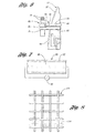
- the seal assembly 22 between the lower and upper housing portions 16 and 18 includes inner and outer seal members 44 and 46 that extend around the entire periphery of the housing 12 at its elongated lateral sides 48 shown in Figure 2 as well as its opposite ends 50.
- the inner and outer seal members 44 and 46 are spaced from each other to define an intermediate seal space 54 shown in Figure 5 . This seal space is thus located between the deposition chamber 14 and the ambient 54.
- a vacuum is drawn in the intermediate seal space 54 through a conduit 56 under the control of a valve 58 so as to be of a lesser vacuum than the vacuum in the deposition chamber 14.
- a sensor functions to sense the level of the vacuum in the intermediate seal space 54 to sense leakage of the inner seal member 44 or the outer seal member 46. More specifically, when the sensor 60 senses an increase in the vacuum in the intermediate seal space 54, there is an indication that the inner seal member 44 is permitting leakage. Conversely, when the sensor 60 senses a decrease in the vacuum in the intermediate seal space 54, there is an indication that the outer seal member 46 is leaking.
- the system can monitor both the inner and outer seal members 44 and 46 of the seal assembly 22 to ensure its effective sealing function.
- the seal assembly 22 includes lower and upper seal flanges 62 and 64 on the lower and upper housing portions 16 and 18.
- the inner and outer seal members 44 and 46 extend between the lower and upper seal flanges 62 and 64 as shown in Figure 5 to seal between the lower and upper housing portions.
- guides 66 provide proper positioning of the upper housing portion.
- Clamps 68 shown in Figures 4 and 6 are spaced around the periphery of the housing to secure the seal flanges to each other.
- each clamp has a hydraulic cylinder 70 mounted on the lower seal flange 62 and also has a movable clamp member 74 that engages the upper seal flange 64 and is secured by at least one threaded connector 76 to a piston connecting rod of the hydraulic cylinder.
- the chemical vapor deposition system 10 includes an oven 78 that is located within the housing 12 and has an elongated length corresponding to the length of the housing 12, and the oven has opposite lateral slots 80 through which the roll conveyor 24 and the chemical vapor distributor 26 project from the heated oven.
- the oven 78 has an insulated construction and is mounted on the housing 12 by supports 82 that extend generally radially with respect to the generally circular shape of the housing and the oven.
- the oven 78 includes elongated heaters 84 that extend along the length of the housing.
- Electrical connectors 86 connect the heaters 84 in banks a, b, c, d, and e to control temperature differentials of the glass sheet substrates laterally with respect to the direction of conveyance as well as controlling heating of their upper and lower surfaces to compensate for any radiation and conduction of the lower substrate surfaces provided by the roll conveyor 24.
- Each electrical heater 84 as illustrated in Figure 7 has an electric resistance element 88 across which a voltage 90 is applied, and each heater 84 includes an elongated quartz tube 92 through which the associated electric resistance elements 88 extend so as to be protected.
- the roll conveyor 24 includes a plurality of rolls 94 spaced along the direction of conveyance C along the elongated direction of the direction of conveyance. These conveyor rolls 94 as shown in Figure 4 have ends 96 that project outwardly from the oven 78 through its side slots 80, respectively, adjacent the lateral sides of the housing 12.
- the system housing 12 as illustrated has drive portions 98 whose interiors are in sealed communication with the deposition chamber 14 externally of the oven 78.
- a drive mechanism collectively indicated by 100 is located within the drive portions 98 of the system housing and has vertically extending drive chains 102 that are driven by a gear box 104 and a cross shaft 106 to drive upper drive gear units 108 that engage and rotatively drive the roll ends 98 eternally of the oven 78 but within the housing 12. As such, the drive mechanism 100 is not subjected to the heating involved with the interior of the oven 78 and can be manufactured more economically to function at a lower temperature.
- the conveyor rolls 96 are preferably made from sinter bonded fused silica particles and at locations where the chemical vapor distributor plenums are not located may have annular radiation shields 110 that limit radiant heat loss through the oven side slots 80.
- the system has a screen 112 that is located below the roll conveyor 24 to catch any broken glass sheet substrates.
- the screen 112 is made of stainless steel and includes suitable stiffeners 114, with the stainless steel screen having openings of about 1 to 2 centimeters so as not to disrupt the radiant heat flow from the lower heaters.
Landscapes
- Chemical & Material Sciences (AREA)
- General Chemical & Material Sciences (AREA)
- Chemical Kinetics & Catalysis (AREA)
- Engineering & Computer Science (AREA)
- Materials Engineering (AREA)
- Organic Chemistry (AREA)
- Mechanical Engineering (AREA)
- Metallurgy (AREA)
- Life Sciences & Earth Sciences (AREA)
- Geochemistry & Mineralogy (AREA)
- Chemical Vapour Deposition (AREA)
- Physical Vapour Deposition (AREA)
Applications Claiming Priority (2)
| Application Number | Priority Date | Filing Date | Title |
|---|---|---|---|
| US09/931,470 US6719848B2 (en) | 2001-08-16 | 2001-08-16 | Chemical vapor deposition system |
| EP02794855A EP1440179B1 (de) | 2001-08-16 | 2002-08-07 | System zur chemischen gasphasenabscheidung |
Related Parent Applications (2)
| Application Number | Title | Priority Date | Filing Date |
|---|---|---|---|
| EP02794855A Division EP1440179B1 (de) | 2001-08-16 | 2002-08-07 | System zur chemischen gasphasenabscheidung |
| EP02794855.3 Division | 2002-08-07 |
Publications (2)
| Publication Number | Publication Date |
|---|---|
| EP2316986A1 true EP2316986A1 (de) | 2011-05-04 |
| EP2316986B1 EP2316986B1 (de) | 2012-10-03 |
Family
ID=25460820
Family Applications (2)
| Application Number | Title | Priority Date | Filing Date |
|---|---|---|---|
| EP11152605A Expired - Lifetime EP2316986B1 (de) | 2001-08-16 | 2002-08-07 | System zur chemischen Gasphasenabscheidung |
| EP02794855A Expired - Lifetime EP1440179B1 (de) | 2001-08-16 | 2002-08-07 | System zur chemischen gasphasenabscheidung |
Family Applications After (1)
| Application Number | Title | Priority Date | Filing Date |
|---|---|---|---|
| EP02794855A Expired - Lifetime EP1440179B1 (de) | 2001-08-16 | 2002-08-07 | System zur chemischen gasphasenabscheidung |
Country Status (5)
| Country | Link |
|---|---|
| US (1) | US6719848B2 (de) |
| EP (2) | EP2316986B1 (de) |
| JP (2) | JP2004538373A (de) |
| TW (1) | TWI281949B (de) |
| WO (1) | WO2003016586A1 (de) |
Families Citing this family (57)
| Publication number | Priority date | Publication date | Assignee | Title |
|---|---|---|---|---|
| US20030044539A1 (en) * | 2001-02-06 | 2003-03-06 | Oswald Robert S. | Process for producing photovoltaic devices |
| US20060071384A1 (en) * | 2004-10-06 | 2006-04-06 | Advanced Display Process Engineering Co. Ltd. | Apparatus for manufacturing flat-panel display |
| US7794667B2 (en) * | 2005-10-19 | 2010-09-14 | Moore Epitaxial, Inc. | Gas ring and method of processing substrates |
| WO2007106502A2 (en) * | 2006-03-13 | 2007-09-20 | Nanogram Corporation | Thin silicon or germanium sheets and photovoltaics formed from thin sheets |
| US9017480B2 (en) * | 2006-04-06 | 2015-04-28 | First Solar, Inc. | System and method for transport |
| US8603250B2 (en) * | 2006-06-27 | 2013-12-10 | First Solar, Inc. | System and method for deposition of a material on a substrate |
| CN101680091A (zh) * | 2007-06-15 | 2010-03-24 | 纳克公司 | 反应性气流沉积和无机箔的合成 |
| TW201002466A (en) * | 2008-04-10 | 2010-01-16 | Applied Materials Inc | Laser-scribing platform |
| TW201006600A (en) * | 2008-04-10 | 2010-02-16 | Applied Materials Inc | Laser-scribing platform and hybrid writing strategy |
| US20090314751A1 (en) * | 2008-04-11 | 2009-12-24 | Applied Materials, Inc. | Laser scribe inspection methods and systems |
| US20090321399A1 (en) * | 2008-04-11 | 2009-12-31 | Applied Materials, Inc. | Dynamic scribe alignment for laser scribing, welding or any patterning system |
| US20090314752A1 (en) * | 2008-05-14 | 2009-12-24 | Applied Materials, Inc. | In-situ monitoring for laser ablation |
| DE102008045369B4 (de) * | 2008-09-02 | 2013-11-21 | Grenzebach Maschinenbau Gmbh | Vorrichtung und Verfahren zum Aufnehmen von Glasplatten |
| KR20110089356A (ko) * | 2008-11-19 | 2011-08-05 | 어플라이드 머티어리얼스, 인코포레이티드 | 레이저-스크라이빙 도구 구조 |
| US20100126580A1 (en) * | 2008-11-26 | 2010-05-27 | Farrell James F | CdTe deposition process for solar cells |
| US20100212358A1 (en) * | 2009-02-26 | 2010-08-26 | Applied Materials, Inc. | Glass substrate orientation inspection methods and systems for photo voltaics production |
| US8333843B2 (en) * | 2009-04-16 | 2012-12-18 | Applied Materials, Inc. | Process to remove metal contamination on a glass substrate |
| US20100269853A1 (en) * | 2009-04-27 | 2010-10-28 | Applied Materials, Inc. | Debris-extraction exhaust system |
| US8418418B2 (en) | 2009-04-29 | 2013-04-16 | 3Form, Inc. | Architectural panels with organic photovoltaic interlayers and methods of forming the same |
| TW201103681A (en) * | 2009-06-12 | 2011-02-01 | Applied Materials Inc | Methods and systems for laser-scribed line alignment |
| WO2011017570A2 (en) * | 2009-08-06 | 2011-02-10 | Applied Materials, Inc. | In-line metrology methods and systems for solar cell fabrication |
| DE112010003736T5 (de) * | 2009-08-06 | 2013-02-28 | Applied Materials, Inc. | Ritzen von quer verlaufenden ISO-Linien, verknüpfen, und vereinfachte Laser- und Scannersteuerungen |
| US20110132884A1 (en) * | 2009-08-06 | 2011-06-09 | Applied Materials, Inc. | Laser modules and processes for thin film solar panel laser scribing |
| WO2011017569A2 (en) * | 2009-08-06 | 2011-02-10 | Applied Materials, Inc. | Methods and related systems for thin-film laser scribing with enhanced throughput |
| WO2011056900A2 (en) * | 2009-11-03 | 2011-05-12 | Applied Materials, Inc. | Multi-wavelength laser-scribing tool |
| US20110139073A1 (en) * | 2009-12-15 | 2011-06-16 | Primestar Solar, Inc. | Conveyor assembly for a vapor deposition apparatus |
| US8187555B2 (en) * | 2009-12-15 | 2012-05-29 | Primestar Solar, Inc. | System for cadmium telluride (CdTe) reclamation in a vapor deposition conveyor assembly |
| US8481355B2 (en) * | 2009-12-15 | 2013-07-09 | Primestar Solar, Inc. | Modular system and process for continuous deposition of a thin film layer on a substrate |
| US8247255B2 (en) * | 2009-12-15 | 2012-08-21 | PrimeStar, Inc. | Modular system and process for continuous deposition of a thin film layer on a substrate |
| US20110139247A1 (en) * | 2009-12-16 | 2011-06-16 | Primestar Solar, Inc. | Graded alloy telluride layer in cadmium telluride thin film photovoltaic devices and methods of manufacturing the same |
| US8163089B2 (en) * | 2009-12-16 | 2012-04-24 | Primestar Solar, Inc. | Vapor deposition apparatus and process for continuous deposition of a thin film layer on a substrate |
| US8430966B2 (en) * | 2009-12-16 | 2013-04-30 | Primestar Solar, Inc. | Vapor deposition apparatus and process for continuous deposition of a thin film layer on a substrate |
| KR101415552B1 (ko) * | 2009-12-21 | 2014-07-07 | 주식회사 미코 | 접지구조물, 이를 구비하는 히터 및 화학기상 증착장치 |
| US8430963B2 (en) * | 2010-01-07 | 2013-04-30 | Primestar Solar, Inc. | Cool-down system and method for a vapor deposition system |
| US8252117B2 (en) * | 2010-01-07 | 2012-08-28 | Primestar Solar, Inc. | Automatic feed system and related process for introducing source material to a thin film vapor deposition system |
| US8361229B2 (en) | 2010-04-22 | 2013-01-29 | Primestar Solar, Inc. | Seal configuration for a system for continuous deposition of a thin film layer on a substrate |
| US8409407B2 (en) | 2010-04-22 | 2013-04-02 | Primestar Solar, Inc. | Methods for high-rate sputtering of a compound semiconductor on large area substrates |
| US8252619B2 (en) | 2010-04-23 | 2012-08-28 | Primestar Solar, Inc. | Treatment of thin film layers photovoltaic module manufacture |
| US8361232B2 (en) | 2010-04-29 | 2013-01-29 | Primestar Solar, Inc. | Vapor deposition apparatus and process for continuous indirect deposition of a thin film layer on a substrate |
| TWI477646B (zh) * | 2010-08-09 | 2015-03-21 | Hon Hai Prec Ind Co Ltd | 化學氣相沉積設備 |
| US8187386B2 (en) | 2010-12-22 | 2012-05-29 | Primestar Solar, Inc. | Temporally variable deposition rate of CdTe in apparatus and process for continuous deposition |
| US8771421B2 (en) | 2010-12-23 | 2014-07-08 | First Solar, Inc. | Entrance and exit roll seal configuration for a vapor deposition system |
| US8247741B2 (en) | 2011-03-24 | 2012-08-21 | Primestar Solar, Inc. | Dynamic system for variable heating or cooling of linearly conveyed substrates |
| US8986785B2 (en) * | 2011-06-23 | 2015-03-24 | Surface Activation Technologies | Method and apparatus for continuous sulfonization of discrete article |
| DE102011080202A1 (de) * | 2011-08-01 | 2013-02-07 | Gebr. Schmid Gmbh | Vorrichtung und Verfahren zur Herstellung von dünnen Schichten |
| US8677932B2 (en) | 2011-08-03 | 2014-03-25 | First Solar, Inc. | Apparatus for metering granular source material in a thin film vapor deposition apparatus |
| US8673777B2 (en) | 2011-09-30 | 2014-03-18 | First Solar, Inc. | In-line deposition system and process for deposition of a thin film layer |
| JP5779804B2 (ja) * | 2011-10-12 | 2015-09-16 | 日東電工株式会社 | 有機エレクトロルミネッセンス素子の製造方法 |
| US8722136B2 (en) | 2011-10-21 | 2014-05-13 | First Solar, Inc. | Heat strengthening of a glass superstrate for thin film photovoltaic devices |
| US9692039B2 (en) | 2012-07-24 | 2017-06-27 | Quantumscape Corporation | Nanostructured materials for electrochemical conversion reactions |
| DE202012103945U1 (de) | 2012-10-16 | 2012-10-25 | Von Ardenne Anlagentechnik Gmbh | Dichtung für Substratbehandlungskammer |
| US20140110225A1 (en) * | 2012-10-24 | 2014-04-24 | Primestar Solar, Inc. | Conveyor assembly with geared, removable rollers for a vapor deposition system |
| US10158115B2 (en) | 2013-06-06 | 2018-12-18 | Quantumscape Corporation | Flash evaporation of solid state battery component |
| US9093599B2 (en) | 2013-07-26 | 2015-07-28 | First Solar, Inc. | Vapor deposition apparatus for continuous deposition of multiple thin film layers on a substrate |
| TWI495748B (zh) * | 2013-11-28 | 2015-08-11 | Metal Ind Res & Dev Ct | 鍍膜設備 |
| WO2015130831A1 (en) | 2014-02-25 | 2015-09-03 | Quantumscape Corporation | Hybrid electrodes with both intercalation and conversion materials |
| WO2016025866A1 (en) | 2014-08-15 | 2016-02-18 | Quantumscape Corporation | Doped conversion materials for secondary battery cathodes |
Citations (10)
| Publication number | Priority date | Publication date | Assignee | Title |
|---|---|---|---|---|
| GB2159145A (en) * | 1984-05-24 | 1985-11-27 | Kyro Oy | Apparatus for equalizing the temperature of conveyor rolls in a glass-tempering furnace |
| US5223001A (en) * | 1991-11-21 | 1993-06-29 | Tokyo Electron Kabushiki Kaisha | Vacuum processing apparatus |
| US5248349A (en) | 1992-05-12 | 1993-09-28 | Solar Cells, Inc. | Process for making photovoltaic devices and resultant product |
| US5571331A (en) * | 1994-03-16 | 1996-11-05 | Balzers Aktiengesellschaft | Vacuum treatment apparatus |
| US5772715A (en) | 1997-01-17 | 1998-06-30 | Solar Cells, Inc. | System and method for processing sheet glass |
| US5938851A (en) * | 1997-04-14 | 1999-08-17 | Wj Semiconductor Equipment Group, Inc. | Exhaust vent assembly for chemical vapor deposition systems |
| US5945163A (en) | 1998-02-19 | 1999-08-31 | First Solar, Llc | Apparatus and method for depositing a material on a substrate |
| US5976260A (en) * | 1992-09-07 | 1999-11-02 | Mitsubishi Denki Kabushiki Kaisha | Semiconductor producing apparatus, and wafer vacuum chucking device, gas cleaning method and nitride film forming method in semiconductor producing apparatus |
| US6025013A (en) * | 1994-03-29 | 2000-02-15 | Schott Glaswerke | PICVD process and device for the coating of curved substrates |
| US6037241A (en) | 1998-02-19 | 2000-03-14 | First Solar, Llc | Apparatus and method for depositing a semiconductor material |
Family Cites Families (28)
| Publication number | Priority date | Publication date | Assignee | Title |
|---|---|---|---|---|
| US2391970A (en) * | 1943-12-07 | 1946-01-01 | Nat Lock Washer Co | Continuous furnace |
| US3223498A (en) * | 1962-02-27 | 1965-12-14 | Pittsburgh Plate Glass Co | Heat treatment of conveyed glass and apparatus therefor |
| US3541293A (en) * | 1968-10-29 | 1970-11-17 | Ronald Macdonald | Muffle furnace |
| DE1913676A1 (de) * | 1969-03-18 | 1970-09-24 | Siemens Ag | Verfahren zum Abscheiden von Schichten aus halbleitendem bzw. isolierendem Material aus einem stroemenden Reaktionsgas auf erhitzte Halbleiterkristalle bzw. zum Dotieren solcher Kristalle aus einem stroemenden dotierenden Gas |
| BE792701A (de) * | 1971-12-14 | 1973-03-30 | Arbed | |
| US4040372A (en) * | 1975-09-19 | 1977-08-09 | Flanders Robert D | Method for detachably sealing together the sections of a barrel container assembly |
| JPS58158914A (ja) * | 1982-03-16 | 1983-09-21 | Semiconductor Res Found | 半導体製造装置 |
| JPS58196063A (ja) * | 1982-05-10 | 1983-11-15 | Matsushita Electric Ind Co Ltd | 光起電力素子の製造方法 |
| JPS60200468A (ja) * | 1984-03-23 | 1985-10-09 | Hitachi Ltd | 燃料電池 |
| JPS62170481A (ja) * | 1986-01-24 | 1987-07-27 | Dainippon Screen Mfg Co Ltd | 管状電気炉 |
| US4920917A (en) * | 1987-03-18 | 1990-05-01 | Teijin Limited | Reactor for depositing a layer on a moving substrate |
| JPH0610679Y2 (ja) * | 1988-12-29 | 1994-03-16 | 株式会社島津製作所 | 連続インライン式成膜装置 |
| JPH0344470A (ja) * | 1989-07-12 | 1991-02-26 | Toshiba Corp | 半導体基板の薄膜形成装置 |
| US4983202A (en) * | 1990-02-27 | 1991-01-08 | Libbey-Owens-Ford Co. | Glass sheet heating furnace and method of using |
| JP3106172B2 (ja) * | 1991-02-26 | 2000-11-06 | 東京エレクトロン株式会社 | 熱処理装置の封止構造 |
| JP2994797B2 (ja) * | 1991-06-27 | 1999-12-27 | 三洋電機株式会社 | 透明電極層の形成方法とその製造装置 |
| JPH06151365A (ja) * | 1992-11-13 | 1994-05-31 | Hitachi Ltd | プラズマ処理装置 |
| DE69410301T2 (de) * | 1993-01-29 | 1998-09-24 | Canon Kk | Verfahren zur Herstellung funktioneller niedergeschlagener Schichten |
| US5413671A (en) * | 1993-08-09 | 1995-05-09 | Advanced Micro Devices, Inc. | Apparatus and method for removing deposits from an APCVD system |
| US5614249A (en) * | 1995-08-28 | 1997-03-25 | Lsi Logic Corporation | Leak detection system for a gas manifold of a chemical vapor deposition apparatus |
| JPH09263939A (ja) * | 1996-03-26 | 1997-10-07 | Sharp Corp | 加熱装置 |
| JPH09324272A (ja) | 1996-03-31 | 1997-12-16 | Furontetsuku:Kk | シール装置 |
| JP3640478B2 (ja) * | 1996-09-20 | 2005-04-20 | アネルバ株式会社 | プラズマ処理装置 |
| AU5178898A (en) | 1997-01-17 | 1998-08-07 | Solar Cells, Inc. | Processing system and method for processing discrete sheets |
| US6207591B1 (en) * | 1997-11-14 | 2001-03-27 | Kabushiki Kaisha Toshiba | Method and equipment for manufacturing semiconductor device |
| JP2003517405A (ja) * | 1998-07-01 | 2003-05-27 | インテバック・インコーポレイテッド | 高速熱処理システム用基板輸送組立体 |
| KR100687971B1 (ko) * | 1998-12-30 | 2007-02-27 | 동경 엘렉트론 주식회사 | 챔버 하우징 및 플라즈마원 |
| JP2001205527A (ja) * | 2000-01-28 | 2001-07-31 | Toshiba Mach Co Ltd | 工作機械および工作機械のテーブルをクランプする方法 |
-
2001
- 2001-08-16 US US09/931,470 patent/US6719848B2/en not_active Expired - Lifetime
-
2002
- 2002-08-07 WO PCT/US2002/024924 patent/WO2003016586A1/en not_active Ceased
- 2002-08-07 EP EP11152605A patent/EP2316986B1/de not_active Expired - Lifetime
- 2002-08-07 EP EP02794855A patent/EP1440179B1/de not_active Expired - Lifetime
- 2002-08-07 JP JP2003520872A patent/JP2004538373A/ja active Pending
- 2002-08-15 TW TW091118451A patent/TWI281949B/zh not_active IP Right Cessation
-
2010
- 2010-01-06 JP JP2010001397A patent/JP5438521B2/ja not_active Expired - Fee Related
Patent Citations (13)
| Publication number | Priority date | Publication date | Assignee | Title |
|---|---|---|---|---|
| GB2159145A (en) * | 1984-05-24 | 1985-11-27 | Kyro Oy | Apparatus for equalizing the temperature of conveyor rolls in a glass-tempering furnace |
| US5223001A (en) * | 1991-11-21 | 1993-06-29 | Tokyo Electron Kabushiki Kaisha | Vacuum processing apparatus |
| US5248349A (en) | 1992-05-12 | 1993-09-28 | Solar Cells, Inc. | Process for making photovoltaic devices and resultant product |
| US5372646A (en) | 1992-05-12 | 1994-12-13 | Solar Cells, Inc. | Apparatus for making photovoltaic devices |
| US5470397A (en) | 1992-05-12 | 1995-11-28 | Solar Cells, Inc. | Process for making photovoltaic devices and resultant product |
| US5536333A (en) | 1992-05-12 | 1996-07-16 | Solar Cells, Inc. | Process for making photovoltaic devices and resultant product |
| US5976260A (en) * | 1992-09-07 | 1999-11-02 | Mitsubishi Denki Kabushiki Kaisha | Semiconductor producing apparatus, and wafer vacuum chucking device, gas cleaning method and nitride film forming method in semiconductor producing apparatus |
| US5571331A (en) * | 1994-03-16 | 1996-11-05 | Balzers Aktiengesellschaft | Vacuum treatment apparatus |
| US6025013A (en) * | 1994-03-29 | 2000-02-15 | Schott Glaswerke | PICVD process and device for the coating of curved substrates |
| US5772715A (en) | 1997-01-17 | 1998-06-30 | Solar Cells, Inc. | System and method for processing sheet glass |
| US5938851A (en) * | 1997-04-14 | 1999-08-17 | Wj Semiconductor Equipment Group, Inc. | Exhaust vent assembly for chemical vapor deposition systems |
| US5945163A (en) | 1998-02-19 | 1999-08-31 | First Solar, Llc | Apparatus and method for depositing a material on a substrate |
| US6037241A (en) | 1998-02-19 | 2000-03-14 | First Solar, Llc | Apparatus and method for depositing a semiconductor material |
Also Published As
| Publication number | Publication date |
|---|---|
| US20030033982A1 (en) | 2003-02-20 |
| EP1440179A1 (de) | 2004-07-28 |
| WO2003016586A1 (en) | 2003-02-27 |
| EP2316986B1 (de) | 2012-10-03 |
| JP2010114458A (ja) | 2010-05-20 |
| JP5438521B2 (ja) | 2014-03-12 |
| JP2004538373A (ja) | 2004-12-24 |
| TWI281949B (en) | 2007-06-01 |
| EP1440179B1 (de) | 2012-01-25 |
| US6719848B2 (en) | 2004-04-13 |
| EP1440179A4 (de) | 2008-07-23 |
Similar Documents
| Publication | Publication Date | Title |
|---|---|---|
| US6719848B2 (en) | Chemical vapor deposition system | |
| US10570516B2 (en) | System and method for transport | |
| TWI625410B (zh) | 用於處理可撓式基板之設備 | |
| EP2762608B1 (de) | Gastrennung durch einstellbare Trennwand | |
| EP2762607B1 (de) | Abscheidungsquelle mit einstellbarer Elektrode | |
| WO1996017106A1 (en) | Apparatus for growing thin films | |
| JP2011520273A (ja) | 処理チャンバ内で物体を焼き戻しするための装置および方法 | |
| EP2762609A1 (de) | Herkömmliche Abscheidungsplattform, Verarbeitungsstation und Betriebsverfahren dafür | |
| US9236282B2 (en) | Arrangement, system, and method for processing multilayer bodies | |
| WO2014046810A1 (en) | Systems and methods for press curing photovoltaic cell module preassemblies | |
| US3904506A (en) | Apparatus for continuous production of sputter-coated glass products | |
| EP1293741A1 (de) | Vorrichtung zur wärmebehandlung | |
| US5772715A (en) | System and method for processing sheet glass | |
| CN102108501B (zh) | 用于衬底上的薄膜层的连续沉积的气相沉积设备和方法 | |
| CN102534510A (zh) | 用于持续地将薄膜层淀积在衬底上的气相淀积设备和过程 | |
| US20070056950A1 (en) | Removable heater | |
| KR20200028134A (ko) | 기판 처리 장치 | |
| US20130064975A1 (en) | Vapor transport deposition system and method employing removable shields | |
| US20110265720A1 (en) | Gas deposition reactor | |
| EP0083383A1 (de) | Verfahren und Vorrichtung zur Erzeugung dünner Filme auf einem sich bewegenden Substrat | |
| CN115449753A (zh) | 一种环境沉积反应设备 | |
| HK1146153A1 (en) | Treatment system for flat substrates | |
| HK1146153B (en) | Treatment system for flat substrates |
Legal Events
| Date | Code | Title | Description |
|---|---|---|---|
| PUAI | Public reference made under article 153(3) epc to a published international application that has entered the european phase |
Free format text: ORIGINAL CODE: 0009012 |
|
| AC | Divisional application: reference to earlier application |
Ref document number: 1440179 Country of ref document: EP Kind code of ref document: P |
|
| AK | Designated contracting states |
Kind code of ref document: A1 Designated state(s): DE ES GB NL |
|
| RIN1 | Information on inventor provided before grant (corrected) |
Inventor name: HINKLE, JAMES E. Inventor name: FAYKOSH, GARY T. Inventor name: FOOTE, JAMES B. |
|
| 17P | Request for examination filed |
Effective date: 20111031 |
|
| GRAP | Despatch of communication of intention to grant a patent |
Free format text: ORIGINAL CODE: EPIDOSNIGR1 |
|
| GRAS | Grant fee paid |
Free format text: ORIGINAL CODE: EPIDOSNIGR3 |
|
| GRAA | (expected) grant |
Free format text: ORIGINAL CODE: 0009210 |
|
| AC | Divisional application: reference to earlier application |
Ref document number: 1440179 Country of ref document: EP Kind code of ref document: P |
|
| AK | Designated contracting states |
Kind code of ref document: B1 Designated state(s): DE ES GB NL |
|
| REG | Reference to a national code |
Ref country code: GB Ref legal event code: FG4D |
|
| REG | Reference to a national code |
Ref country code: DE Ref legal event code: R096 Ref document number: 60243823 Country of ref document: DE Effective date: 20121129 |
|
| REG | Reference to a national code |
Ref country code: NL Ref legal event code: VDEP Effective date: 20121003 |
|
| PG25 | Lapsed in a contracting state [announced via postgrant information from national office to epo] |
Ref country code: ES Free format text: LAPSE BECAUSE OF FAILURE TO SUBMIT A TRANSLATION OF THE DESCRIPTION OR TO PAY THE FEE WITHIN THE PRESCRIBED TIME-LIMIT Effective date: 20130114 Ref country code: NL Free format text: LAPSE BECAUSE OF FAILURE TO SUBMIT A TRANSLATION OF THE DESCRIPTION OR TO PAY THE FEE WITHIN THE PRESCRIBED TIME-LIMIT Effective date: 20121003 |
|
| PLBE | No opposition filed within time limit |
Free format text: ORIGINAL CODE: 0009261 |
|
| STAA | Information on the status of an ep patent application or granted ep patent |
Free format text: STATUS: NO OPPOSITION FILED WITHIN TIME LIMIT |
|
| 26N | No opposition filed |
Effective date: 20130704 |
|
| REG | Reference to a national code |
Ref country code: DE Ref legal event code: R097 Ref document number: 60243823 Country of ref document: DE Effective date: 20130704 |
|
| GBPC | Gb: european patent ceased through non-payment of renewal fee |
Effective date: 20130807 |
|
| PG25 | Lapsed in a contracting state [announced via postgrant information from national office to epo] |
Ref country code: GB Free format text: LAPSE BECAUSE OF NON-PAYMENT OF DUE FEES Effective date: 20130807 |
|
| REG | Reference to a national code |
Ref country code: DE Ref legal event code: R082 Ref document number: 60243823 Country of ref document: DE Representative=s name: D YOUNG & CO LLP, DE |
|
| PGFP | Annual fee paid to national office [announced via postgrant information from national office to epo] |
Ref country code: DE Payment date: 20200827 Year of fee payment: 19 |
|
| REG | Reference to a national code |
Ref country code: DE Ref legal event code: R119 Ref document number: 60243823 Country of ref document: DE |
|
| PG25 | Lapsed in a contracting state [announced via postgrant information from national office to epo] |
Ref country code: DE Free format text: LAPSE BECAUSE OF NON-PAYMENT OF DUE FEES Effective date: 20220301 |