EP2323012A2 - Commutation à économie d'énergie pour un périphérique, périphérique, appareil de transmission et procédé de travail - Google Patents
Commutation à économie d'énergie pour un périphérique, périphérique, appareil de transmission et procédé de travail Download PDFInfo
- Publication number
- EP2323012A2 EP2323012A2 EP10182261A EP10182261A EP2323012A2 EP 2323012 A2 EP2323012 A2 EP 2323012A2 EP 10182261 A EP10182261 A EP 10182261A EP 10182261 A EP10182261 A EP 10182261A EP 2323012 A2 EP2323012 A2 EP 2323012A2
- Authority
- EP
- European Patent Office
- Prior art keywords
- peripheral device
- circuit
- data bus
- data
- energy
- Prior art date
- Legal status (The legal status is an assumption and is not a legal conclusion. Google has not performed a legal analysis and makes no representation as to the accuracy of the status listed.)
- Withdrawn
Links
Images


Classifications
-
- G—PHYSICS
- G06—COMPUTING OR CALCULATING; COUNTING
- G06F—ELECTRIC DIGITAL DATA PROCESSING
- G06F1/00—Details not covered by groups G06F3/00 - G06F13/00 and G06F21/00
- G06F1/26—Power supply means, e.g. regulation thereof
- G06F1/32—Means for saving power
- G06F1/3203—Power management, i.e. event-based initiation of a power-saving mode
- G06F1/3234—Power saving characterised by the action undertaken
- G06F1/325—Power saving in peripheral device
- G06F1/3253—Power saving in bus
-
- Y—GENERAL TAGGING OF NEW TECHNOLOGICAL DEVELOPMENTS; GENERAL TAGGING OF CROSS-SECTIONAL TECHNOLOGIES SPANNING OVER SEVERAL SECTIONS OF THE IPC; TECHNICAL SUBJECTS COVERED BY FORMER USPC CROSS-REFERENCE ART COLLECTIONS [XRACs] AND DIGESTS
- Y02—TECHNOLOGIES OR APPLICATIONS FOR MITIGATION OR ADAPTATION AGAINST CLIMATE CHANGE
- Y02D—CLIMATE CHANGE MITIGATION TECHNOLOGIES IN INFORMATION AND COMMUNICATION TECHNOLOGIES [ICT], I.E. INFORMATION AND COMMUNICATION TECHNOLOGIES AIMING AT THE REDUCTION OF THEIR OWN ENERGY USE
- Y02D10/00—Energy efficient computing, e.g. low power processors, power management or thermal management
-
- Y—GENERAL TAGGING OF NEW TECHNOLOGICAL DEVELOPMENTS; GENERAL TAGGING OF CROSS-SECTIONAL TECHNOLOGIES SPANNING OVER SEVERAL SECTIONS OF THE IPC; TECHNICAL SUBJECTS COVERED BY FORMER USPC CROSS-REFERENCE ART COLLECTIONS [XRACs] AND DIGESTS
- Y02—TECHNOLOGIES OR APPLICATIONS FOR MITIGATION OR ADAPTATION AGAINST CLIMATE CHANGE
- Y02D—CLIMATE CHANGE MITIGATION TECHNOLOGIES IN INFORMATION AND COMMUNICATION TECHNOLOGIES [ICT], I.E. INFORMATION AND COMMUNICATION TECHNOLOGIES AIMING AT THE REDUCTION OF THEIR OWN ENERGY USE
- Y02D30/00—Reducing energy consumption in communication networks
- Y02D30/50—Reducing energy consumption in communication networks in wire-line communication networks, e.g. low power modes or reduced link rate
Definitions
- the present invention relates to a power saving circuit for a peripheral device for connection to a data bus of a host system.
- it relates to a peripheral device and a switching device for a data bus with such energy saving circuit and a working method for such energy saving circuit.
- Peripheral devices for connection to a data bus of a host system are widely known. Examples of such peripheral devices are external storage drives, printers or scanners connected to a host adapter of a computer system. But in other areas of technology, peripheral devices are connected via data buses. Examples include consumer electronics or communications electronics.
- peripheral devices have their own power supply for supplying the peripheral device with an operating voltage. This has the consequence that the peripheral devices are usually supplied with energy even when switching off a host system. Both the peripheral device itself and the power supply unit used to supply the peripheral device cause a power loss. This power loss usually consists to a large extent of losses of switching converters of the power supply.
- an electronic power supply unit which has a control unit, which voltage-transforming elements of a power supply separates depending on a power requirement of a connected electronic device from a primary-side AC voltage.
- the object of the present invention is to describe a power saving circuit for a peripheral device for connection to a data bus of a host system, which reduces a power consumption of the peripheral device in a standby state without disturbing a communication of the data bus.
- peripheral device a switching device and a working method are to be described, which are suitable for use with the energy saving circuit.
- a power-saving circuit for a peripheral device for connection to a data bus of a host system comprising a monitoring circuit for monitoring communication via the data bus, a latch circuit for holding a connection state of the peripheral device and at least one switching element for interrupting a supply voltage for the peripheral device.
- the power save circuit further includes a control circuit configured to detect a start of an idle state of the data bus by the monitor circuit and to hold the connection state of the peripheral device by activating the hold voltage upon detection of a start of the idle state and to supply the power supply to the peripheral device Opening the at least one switching element to interrupt.
- the power saving circuit By holding a connection state of the peripheral device by a latch circuit, even during an idle state of the data bus, the appearance of bus disconnection for the host system can be inhibited. In doing so, during the idle state of the data bus, the power saving circuit performs the function of maintaining a connection state, so that the peripheral device can be disconnected from a power supply voltage without disturbing the communication via the data bus.
- control circuit is further configured to detect an end of an idle state of the data bus by the monitoring circuit.
- the control circuit upon detection of an end of the idle state, restores supply of the peripheral device supply voltage by closing the at least one switching element and enables the connection state of the peripheral device by disabling the latch circuit.
- the additional detection of an end of the idle state and the reconnection of the peripheral device with the supply voltage and the deactivation of the holding circuit For example, the operating state that existed before the idling state started can be restored.
- the host system may transmit data via the data bus at least at a first and a second speed.
- the connection state of the peripheral device determines whether the peripheral device is set for data transmission at the first or second speed.
- the data bus includes at least a first data line and a second data line, and the latch circuit is configured to maintain the first data line at a predetermined voltage level when the peripheral device is set for data transmission at the first speed and to maintain the second data line at a predetermined voltage level when the peripheral device is set up for data transmission at the second speed.
- Such an embodiment of the energy-saving circuit makes it possible to successfully connect the peripheral device to the data bus again after a separation from a supply voltage and to exchange data with the host system at a previously determined speed, without requiring a renewed initialization of the peripheral device or of the host system.
- the energy saving circuit according to the invention is particularly suitable for installation in a peripheral device according to claim 12 or a switching device for a data bus according to claim 13.
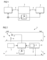
- FIG. 1 shows a first arrangement comprising a host system 1, a peripheral device 2 and an energy saving circuit 3 connected between the host system 1 and the peripheral device 2.
- the host system 1 is, for example, a desktop PC.
- the peripheral device 2 in the exemplary embodiment is a printer which is connected to a host adapter of the host system 1 by means of a serial data bus.
- the peripheral device 2 is connected to the energy-saving circuit 3 with a first data cable 4.
- the energy saving circuit 3 is connected to the host system 1 with a second data cable 5.
- the power saving circuit 3 is electrically connected between the host system 1 and the peripheral device 2, and can monitor communication via the data bus.
- the energy saving circuit 3 comprises a first switching element 6 in the form of a relay.
- the first switching element 6 is between a power supply network that provides an AC line voltage, and the peripheral device 2. By opening the first switching element 6, the power-saving circuit 3 can completely disconnect the peripheral device 2 from the power supply network.
- FIG. 2 shows a schematic representation of the energy saving circuit 3.
- the energy saving circuit 3 comprises in addition to the first switching element 6 for separating a phase line L, a monitoring circuit 7 and a holding circuit 8.
- the energy saving circuit 3 comprises a control circuit 9, the monitoring circuit 7, the holding circuit 8 and first switching element 6 controls.
- the energy saving circuit 6 further includes a switching converter 10 and an energy storage 11th
- a data line D and a reference line GND of the data bus are looped through the energy-saving circuit 3.
- signals received at a first terminal 12 of the deactivated power-saving circuit 3 are also available at the second terminal 13 to which the peripheral device 2 is connected.
- a primary-side mains connection 14 for connecting the energy-saving circuit 3 to a power supply network is connected via the first switching element 6 to a switching output 15 of the energy-saving circuit 3. At the switching output 15, a power supply of the peripheral device 2 is connected.
- the monitoring circuit 7 is set up to monitor a signaling on the data line D of the data bus.
- the monitoring circuit 7 detects whether data is exchanged between the peripheral device 2 and the host system 1 or whether the bus system is in an idle state, in which either no data or a predetermined control signal indicative of the idle state is transmitted. If the presence of such an idling state detected by the monitoring circuit 7, it generates a corresponding control signal for the control circuit. 9
- the control circuit 9 detects the control signal supplied from the monitoring circuit 7 and causes disconnection of the peripheral device 2 from the bus system without disturbing the host system 1.
- the data line D is connected via a so-called pull-down resistor 16 and a transistor 17 to the reference line GND.
- the data line D is pulled via the pull-down resistor 16 to a ground potential of the reference line GND.
- the pull-down resistor 16 replaces a termination of the data bus by the peripheral device 2.
- the control circuit 9 therefore draws the data line D to the potential of the reference line GND upon detection of an idle state of the bus system via the monitoring circuit 7, and then opens the first switching element 6, so that the peripheral device 2 is disconnected from the power supply network and during the idle state of the bus system receives no additional energy from the power grid.
- the control circuit 9 activates the peripheral device 2 again in a manner that is transparent to the host system 1.
- the control circuit 9 for this purpose first activates the peripheral device 2 by closing the first switching element 6.
- the transistor 17 is further driven by the control circuit 9. If the peripheral device 2 is again completely ready for operation, the control signal for the transistor 17 is interrupted by the control circuit 9 and thus the data line D is disconnected from the reference line GND. Subsequently, an undisturbed communication takes place between the peripheral device 2 and the host system 1 via the data line D.
- the data bus according to FIG. 2 In the exemplary embodiment, there is no line for providing a supply voltage.
- the energy saving circuit 3 comprises the additional switching converter 10, which generates a DC voltage for supplying the components of the energy saving circuit 3 from a mains side AC voltage.
- the switching converter 10 is arranged behind the first switching element 6 in the embodiment. Thus, the switching converter 10 is disconnected in the idle state of the bus system from the power supply network.
- the energy storage 11 for example, a rechargeable battery or a high-capacity capacitor stores sufficient electric power to the control circuit 9 for a predetermined standby period, for example, one hour after the idle state is activated, with an operating power supply.
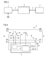
- FIG. 3 shows an alternative arrangement comprising a host system 1, a peripheral device 2 and a power saving circuit 3.
- the host system 1 and the peripheral device 2 in turn connected via a serial data bus, here a USB bus with an integrated power supply line.
- the peripheral device 2 is supplied with an operating voltage via the USB bus.
- the arrangement according to FIG. 3 Therefore, only the host system 1 is connected to a power supply network.
- FIG. 4 shows a schematic representation of the structure of the power-saving circuit 3 for the USB bus system according to FIG. 3
- Both a first terminal 12 and a second terminal 13 of the energy saving circuit 3 each comprise two differential data lines D + and D- and two supply lines VCC and GND. These lines are looped through the energy-saving circuit 3, wherein the supply line VCC can be separated by means of a second switching element 18.
- the second switching element 18 is a field effect transistor.
- the energy-saving circuit after FIG. 4 has a monitoring circuit 7, a control circuit 9 and a holding circuit 8.
- the monitoring circuit 7 and the control circuit 9 are integrated in a common microcontroller 19.
- the holding circuit 8 comprises a first transistor 17a and a second transistor 17b for connecting the first data line D + via a first resistor 16a to the supply line VCC and the second data line D- via a second resistor 16b to the supply line VCC.
- the power-saving circuit 3 has an optional interrupting circuit 20.
- the interruption circuit 20 comprises two third switching elements 21a and 21b, through which the data lines D + and D- between the first terminal 12 and the second terminal 13 can be separated. As a result, leakage currents in the direction of a peripheral device 2 connected to the second connection 13 can be prevented.
- the interruption circuit 20 By separating the data lines D + and D- by the interruption circuit 20, data transmission between the peripheral device 2 and the host system 1 can also be inhibited even if the peripheral device 2 is supplied with an operating voltage via an external power supply unit. In this way, in particular a waking up of the host system 1 by the peripheral device 2 can be avoided.
- the microcontroller 19 is supplied via the power supply lines VCC and GND with an operating voltage. This is for the sake of clarity in the FIG. 4 but not shown. According to the USB specification, a so-called full power or low power peripheral device in the so-called suspend state may draw 500 pA or 2.5 mA current via the supply line. This is sufficient for the operation of the microcontroller 19 according to the embodiment.
- the monitoring circuit 7 monitors the data bus comprising the data lines D + and D-. In addition to monitoring a signaling of the beginning or the end of an idle state of the data bus, the monitoring circuit 7 also monitors an operating mode of a peripheral device 2 connected to the second connection 13.
- an idle state is initiated on the USB bus in the normal operating state of the host system 1, for example, the ACPI state S0 of the operating system, if the USB peripheral device 2 is not used.
- the peripheral device 2 is placed in the so-called Suspend state. This can also be achieved by a global or selective suspend command of the host system 1.
- a power-saving state such as one of the ACPI conditions S3, S4 or S5
- the host system 1 in the embodiment also sent a suspend command.
- USB peripheral device 2 Once the host system 1 signals an idle state to the peripheral device 2, it must initiate a suspend state within 3 ms. Each USB peripheral device 2 must respond to USB commands from host system 1 immediately, whether it is a global suspend or selective suspend command, or an idle state signaling. Optimized drivers and software running on host system 1 can improve the use of these power-saving modes.
- USB peripheral device 2 is a low-speed (LS), full-speed (FS) or high-speed (HS) device, so-called keep-alive signals usually become available sent via the USB bus.
- LS low-speed
- FS full-speed
- HS high-speed
- keep-alive signals usually become available sent via the USB bus.
- SOF Start of Frame
- USB peripherals 2 must go into suspend state within 3 ms on detection of the constant idle state of the so-called upstream port, so the host system 1 or a higher-level USB hub. After a further 10 ms, peripheral device 2 is only allowed to record the standard-defined suspend current from the USB bus. In the suspend state, the peripheral device 2 must continue to provide a voltage via the data line D + in the high or full speed mode and in the low speed mode via the data line D-, so that the idle state can be maintained. For this purpose, the supply line VCC is connected via a so-called pull-up resistor to the corresponding data line D + or D-. This, together with the upstream host system 1 or USB hub, ensures correct compliance with the USB specification.
- High-speed peripherals 2 There are additional requirements for suspending high-speed peripherals 2 because a reset and an idle state for high-speed peripherals 2 can not be clearly distinguished.
- High-speed peripherals must therefore switch from high-speed mode to full-speed mode after 3 ms idle, or at the latest after 3.125 ms.
- a receiving circuit is separated from the differential data line D + and D- and the data line D + is connected via a pull-up resistor of the peripheral device 2 to the supply line VCC.
- Peripheral device 2 must monitor lines D + and D- no sooner than 100 ⁇ s and not later than 875 ⁇ s after switching to the full-speed mode.
- the peripheral device 2 remains in the suspend state. If so an SEO Start of Packet, so a transition in idle in the so-called K State is detected, then it is a reset signal to reset the peripheral device 2, which is then triggered.
- USB devices indicate whether they are operating in high or full speed mode or low speed mode by pulling up data lines D + and D-, respectively.
- the current bus state is detected and simulated by the connection of the corresponding pull-up resistor 16a or 16b of the latch 8.
- the control circuit 9 activates upon detection of an idle state via the monitoring circuit 7, either the first transistor 17a for signaling a device with a full-speed mode or the second transistor 17b for signaling a device with a low-speed mode. This prevents the host system 1 from detecting a bus separation when the peripheral device 2 is switched off and a reconnection to the bus system when it is switched on again, which would otherwise be signaled to the operating system of the host system 1.
- the energy-saving circuit 3 responds and then controls the second switching element 18 such that the power supply of the peripheral device 2 is interrupted.
- the supply line VCC bus-powered peripherals 2 can be separated from the supply voltage without a connected to the first terminal 12 host system 1 notices the deactivation of the peripheral device 2.
- the data lines D + and D- are separated via the interruption circuit 20.
- a peripheral device 2 For a peripheral device 2 to return from the suspend state, it must be woken up via a so-called resume sequence.
- a peripheral device 2 starts the resume as soon as another bus state (English: non-idle state) than the idle state is applied to the upstream port. So-called wakeup-enabled USB peripheral devices 2 can also wake the host system 1 from the suspend state.
- the host system 1 is always entitled to send the resume sequence (TDRSMDN) which is on the bus for at least 20ms. Depending on the device speed, the host system must terminate the resume sequence with two different end sequences. For full and low-speed peripherals 2, a low-speed EOP (end-of-packet: two low-speed bit periods of single-ended SEO followed by a J state) is signaled. If the peripheral device was in the high-speed mode when it was suspended, resume signaling must be initiated with a high-speed idle sequence. The control of the host system 1 must additionally ensure a 10 ms long resume recovery time (TRSMRCY) before the awakened peripherals 2 may be accessed.
- TRSMRCY resume recovery time
- the host system 1 initiates the resume state by means of a level change on the data lines D + and D-, this is detected by the monitoring circuit 7 and evaluated by the control circuit 8. Then, the supply voltage is switched through the second switching element 18 again to the second terminal 13, and the pull-up resistors 16a and 16b are separated from the data lines D + and D-.
- the optional interruption circuit 20 then becomes optional deactivated to restore a connection of the data lines between the first terminal 12 and the second terminal 13. In the exemplary embodiment, this takes place synchronously with the deactivation of the transistors 17a and 17b, so that an uninterrupted takeover by a device-internal pull-up resistor takes place and thus no device separation is triggered. Thereafter, the peripheral device 2 returns from the suspend state to the normal operating state in consideration of the time requirements of the USB specification.
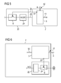
- FIG. 5 shows a peripheral device 2 with an external power supply 22.
- the peripheral device 2 according to FIG. 5 includes a power-saving circuit 3.
- the power-saving circuit 3 is similar to that in the FIG. 2 constructed energy saving circuit 3 and provides a control signal via a control signal output 23 to the peripheral device 2 ready.
- the control signal from the control output 23 is used to interrupt a power supply to the external power supply 22.
- the power supply 22 includes a first switching element 6 for disconnecting a converter circuit 24 from a power supply network.
- the power supply 22 and the peripheral device 2 are connected to each other via a supply line 25 for transmitting a DC voltage.
- they are connected to one another by an additional control line 26 for transmitting the control signal from the control output 23 to the first switching element 6 of the power supply 22.
- control signal of the control output 23 can also be modulated onto the supply line 25 for transmitting the supply voltage.
- a high-frequency AC voltage signal can be modulated onto a DC supply voltage.
- FIG. 6 shows a peripheral device 2 with an internal power supply 22.
- the operation of the peripheral device 2 according to FIG. 6 largely corresponds to that of the peripheral device 2 in FIG. 5 , Since the power supply 22 according to FIG. 6 However, integrated into the peripheral device 2, can be dispensed with an external connection between the peripheral device 2 and the power supply 22, which in particular facilitates the control of the first switching element 6 of the power supply 22.
- FIG. 7 shows a switching device 27 for connecting two peripheral devices 2a and 2b to a common host system 1.
- the first peripheral device 2a is remotely powered via a data bus from the switching device 27 with an operating power.
- the first peripheral device 2a with a bus line 28a, which includes both data lines and supply lines, connected to the switching device 27.
- the second peripheral device 2b is supplied with an operating power by an external power supply 22.
- the second peripheral device 2b is connected to the switching device 27 via a second bus line 28b.
- the power supply 22 is connected to a switching output 15b of the switching device 27.
- it is a switchable socket, which is associated with a second terminal 13b for the second peripheral device 2b.
- the switching device 27 comprises a power saving circuit 3, which is constructed similar to those described above. Specifically, the power saving circuit 3 monitors the communication between the host system 1 and the peripherals 2a and 2b. When no data is transmitted from the host system 1 to the peripheral devices 2a or 2b, the first peripheral device 2a and the second peripheral device 2b, respectively, become one Power supply disconnected. In the case of the supplied via the switching device 27 peripheral device 2a only one supply line of the bus line 28a is interrupted for this purpose, as for example with reference to the FIG. 4 has been described. In the case of the second peripheral device 2b, the switching output 15b of the switching device 27 configured as a socket is deactivated so that the power pack 22 is disconnected from the power supply network.
- a switching converter 10 of the switching device 27 can also be disconnected from the power supply network.
- the power-saving circuit 3 is supplied with an operating power either from the host system 1 or from an internal energy store of the switching device 27, as described above.
- FIG. 8 shows an exemplary signaling of an idle state via a USB bus.
- a host system 1 in the exemplary embodiment a personal computer, is in a normal operating state, for example the so-called ACPI operating state S0.
- a data transmission takes place via differential data lines D + and D- of a USB bus.
- data packets with a frame duration of one millisecond are sent either via the USB low-speed standard or according to the USB full-speed standard via the data lines D + and D-.
- the host system 1 If no further data is to be exchanged between the host system 1 and the peripheral device 2, the host system 1 signals an idle state at a time T1. In this state, neither data nor control signals are exchanged over the data lines D + and D-. In particular, not even so-called start-off-frame (SOF) packets are sent over the data bus in this bus operating state.
- SOF start-off-frame
- the power-saving circuit 3 After a predetermined idle time Tidle of at least three milliseconds, the power-saving circuit 3 detects that there is no activity on the data bus. Then, depending on a predetermined transmission mode, it pulls either the positive data line D + or the negative data line D- to a predetermined voltage level. Thereafter, a corresponding control signal for interrupting a primary mains voltage and / or a secondary DC voltage of a supply line of the data bus is generated. In this way, it is ensured that the peripheral device 2 does not receive any further energy in the idle state of the bus system.
- the peripheral device 2 is reconnected to the data bus.
- the energy saving circuit 3 first detects a resumption of the signaling via the data bus. For example, an explicit resume signal is provided by the host system 1. Alternatively, it is also possible to detect data packets with a preceding SOF signal.
- the control circuit 9 activates first the first switching element 6 and / or the second switching element 18 for providing a mains voltage to a power supply 22 or a supply voltage via a supply line of the data bus.
- the peripheral device 2 starts running and is in an operational state within a predefined period of time Tstart. Thereafter, the latch circuit 8 is de-activated by canceling the corresponding control signals for pulling up the positive data line D + and the negative data line D, respectively.
- the data is processed by the peripheral device 2 and communication with the host system 1 is continued.
- the host system 1 does not generate a corresponding interrupt which is normally evaluated by an operating system of the host system 1 when other peripheral devices 2 are connected.
- FIG. 9 shows a flowchart of a working procedure for a power saving circuit 3.
- a first step A1 it is monitored in a loop whether the bus system is in an idle state. If the bus system is not in an idle state, a timer for determining an idle time is reset in a step A2. Steps A1 and A2 are repeated until an idle state is detected.
- step A3 If the bus system is in an idling state, a check is made in a subsequent step A3 as to whether a predetermined period for applying the idling state has been reached. For example, it checks to see if a USB bus is in an idle state for more than three milliseconds. If this is not yet the case, the method continues in step A1.
- a connection state of a peripheral device 2 is detected in a step A4. For example, it is detected whether a peripheral device 2 communicates with a host system 1 in a so-called low-speed or in a full-speed mode. Separate monitoring for the use of a high-speed mode is not required because peripheral devices that communicate in the high-speed mode first change back to the full-speed mode before transitioning to an idle state.
- a holding circuit 8 is then activated first.
- a resistor 16 is connected across a transistor 17 between a data line and a supply line to pull the data line to a predetermined voltage level.
- a switching element 6 and / or a second switching element 18 is opened in order to prevent a power supply of the peripheral device 2.
- the peripheral device 2 therefore does not receive any further electrical energy from a power supply network.
- the energy saving circuit 3 is suitable for integration into individual devices, as a separate additional circuit arranged between a host system 1 and a peripheral device 2 and for arrangement in switching components such as a USB hub or switch.
- the solution described is suitable in addition to the USB bus for other bus systems, the detection of an idle state allow.
- it is suitable for bus systems that include a supply line, which allows a supply of energy-saving circuit 3 via the bus system, even when peripheral devices are switched off.
- bus systems include eSATA, Firewire (IEEE 1394), external PCI Express and Power over Ethernet (PoE, IEEE 802.3af).
- An energy saving can be improved by further optimizing a host-side control of the bus system.
- it can be specified in an operating system from which period of inactivity of a single device either the entire bus system or individual peripheral devices 2 connected to the bus system are to be put into a suspend state.
- the host system 1 is configured so that when switched to a power-saving state, for example, an ACPI S3, S4 or S5 state, the data bus is basically placed in an idle state, so that connected to the data bus peripherals 2 together with the host system 1 in go over a power saving state.
- the idle state signaling is not tied to a particular protocol layer.
- a supply line of a data bus is deactivated in an energy-saving state of the host system 1. If the monitoring circuit 7 recognizes a deactivation of a supply voltage on one of the supply lines, this can likewise be used to detect an idle state and for the subsequent deactivation of a peripheral device 2.
Landscapes
- Engineering & Computer Science (AREA)
- Theoretical Computer Science (AREA)
- Physics & Mathematics (AREA)
- General Engineering & Computer Science (AREA)
- General Physics & Mathematics (AREA)
- Power Sources (AREA)
Applications Claiming Priority (1)
| Application Number | Priority Date | Filing Date | Title |
|---|---|---|---|
| DE102009052947A DE102009052947B3 (de) | 2009-11-12 | 2009-11-12 | Energiesparschaltung für ein Peripheriegerät, Peripheriegerät, Vermittlungsgerät und Arbeitsverfahren |
Publications (2)
| Publication Number | Publication Date |
|---|---|
| EP2323012A2 true EP2323012A2 (fr) | 2011-05-18 |
| EP2323012A3 EP2323012A3 (fr) | 2014-07-02 |
Family
ID=43070077
Family Applications (1)
| Application Number | Title | Priority Date | Filing Date |
|---|---|---|---|
| EP10182261.7A Withdrawn EP2323012A3 (fr) | 2009-11-12 | 2010-09-29 | Commutation à économie d'énergie pour un périphérique, périphérique, appareil de transmission et procédé de travail |
Country Status (4)
| Country | Link |
|---|---|
| US (1) | US8527798B2 (fr) |
| EP (1) | EP2323012A3 (fr) |
| JP (1) | JP5628640B2 (fr) |
| DE (1) | DE102009052947B3 (fr) |
Cited By (1)
| Publication number | Priority date | Publication date | Assignee | Title |
|---|---|---|---|---|
| CN104484024A (zh) * | 2011-12-12 | 2015-04-01 | 威盛电子股份有限公司 | 桥接装置以及桥接装置的省电操作方法 |
Families Citing this family (13)
| Publication number | Priority date | Publication date | Assignee | Title |
|---|---|---|---|---|
| US20120257426A1 (en) * | 2011-04-11 | 2012-10-11 | Ever Win International Corporation | AC Adapter With Automatic Built-In Power Switch |
| US10817043B2 (en) * | 2011-07-26 | 2020-10-27 | Nvidia Corporation | System and method for entering and exiting sleep mode in a graphics subsystem |
| GB2509124A (en) * | 2012-12-21 | 2014-06-25 | Nomad Spectrum Ltd | Wireless access point and cellular network relay with secondary co-processor controlling power supplies and SIM cards |
| KR20140140438A (ko) | 2013-05-29 | 2014-12-09 | 삼성전자주식회사 | Usb 유휴 상태 대기 시간을 동적으로 조절하는 usb 시스템 및 그 동작방법 |
| EP2899641B1 (fr) * | 2014-01-22 | 2018-08-22 | Harman Becker Automotive Systems GmbH | Serveur de dispositif USB multimédia |
| US9804650B2 (en) * | 2014-09-04 | 2017-10-31 | Qualcomm Incorporated | Supply voltage node coupling using a switch |
| MY184148A (en) * | 2015-12-25 | 2021-03-23 | Intel Corp | Power management system |
| JP6396352B2 (ja) * | 2016-03-11 | 2018-09-26 | 株式会社東芝 | 半導体装置 |
| US10915484B2 (en) * | 2017-02-24 | 2021-02-09 | Digital 14 Llc | Peripheral disconnection switch system and method |
| US10809758B2 (en) | 2017-04-24 | 2020-10-20 | Cirrus Logic, Inc. | Recovery of reference clock on a device |
| EP4099566B1 (fr) * | 2020-02-14 | 2025-04-09 | Huawei Technologies Co., Ltd. | Circuit intégré, procédé et système de commande |
| DE102024108227A1 (de) * | 2024-03-22 | 2025-09-25 | Connaught Electronics Ltd. | Verfahren zum Betreiben eines Steuergeräts, Steuergerät sowie Kraftfahrzeug |
| DE102024208629A1 (de) | 2024-09-11 | 2026-03-12 | Robert Bosch Gesellschaft mit beschränkter Haftung | Schnittstelleneinrichtung und Recheneinheit mit Schnittstelleneinrichtung |
Citations (1)
| Publication number | Priority date | Publication date | Assignee | Title |
|---|---|---|---|---|
| DE102007052880A1 (de) | 2007-11-02 | 2009-05-14 | Fujitsu Siemens Computers Gmbh | Elektronische Stromversorgungseinheit, elektronisches Peripheriegerät, sowie Verfahren zur Steuerung einer Stromversorgungseinheit |
Family Cites Families (24)
| Publication number | Priority date | Publication date | Assignee | Title |
|---|---|---|---|---|
| JPH0812578B2 (ja) * | 1989-09-06 | 1996-02-07 | セイコー電子工業株式会社 | 半導体集積回路装置 |
| JPH04155418A (ja) | 1990-10-19 | 1992-05-28 | Toshiba Corp | 論理回路 |
| JPH07230346A (ja) * | 1994-02-17 | 1995-08-29 | Hitachi Ltd | 電力制御装置 |
| DE19732675C2 (de) * | 1997-07-29 | 1999-11-25 | Siemens Ag | Schaltung zum bedarfsgerechten Ein- und Ausschalten eines Verbrauchers |
| US6119194A (en) * | 1998-03-19 | 2000-09-12 | Advanced Micro Devices, Inc. | Method and apparatus for monitoring universal serial bus activity |
| JPH11305880A (ja) * | 1998-04-23 | 1999-11-05 | Sony Corp | Usb機器およびusbハブ装置 |
| JP2001067156A (ja) * | 1999-08-27 | 2001-03-16 | Canon Inc | コンピュータ周辺機器及びその制御方法、撮像装置並びに記憶媒体 |
| JP2001088631A (ja) | 1999-09-24 | 2001-04-03 | Matsushita Electric Ind Co Ltd | 車載通信端末装置 |
| US6816976B2 (en) * | 2001-03-29 | 2004-11-09 | Cypress Semiconductor Corp. | System and method for reducing power consumption in a universal serial bus device |
| KR100711914B1 (ko) * | 2001-09-15 | 2007-04-27 | 엘지전자 주식회사 | 유에스비 전원 제어장치 |
| JP3675394B2 (ja) * | 2001-11-30 | 2005-07-27 | ソニー株式会社 | 通信デバイス |
| JP4076408B2 (ja) | 2002-09-04 | 2008-04-16 | 川崎マイクロエレクトロニクス株式会社 | Usb用レジュームコントロール装置 |
| AU2003282290A1 (en) * | 2002-10-18 | 2004-05-04 | Thomson Licensing S.A. | Bus controlled power switch |
| JP4529441B2 (ja) * | 2004-01-05 | 2010-08-25 | 富士ゼロックス株式会社 | 画像処理装置およびホスト装置 |
| TWI248568B (en) * | 2004-05-24 | 2006-02-01 | Avision Inc | Power-saving system of computer peripheral apparatus |
| JP2006171868A (ja) | 2004-12-13 | 2006-06-29 | Canon Inc | 印字装置 |
| JP4731995B2 (ja) * | 2005-05-18 | 2011-07-27 | キヤノン株式会社 | 電子機器装置及びその処理方法 |
| JP4125328B2 (ja) | 2006-04-17 | 2008-07-30 | キヤノン株式会社 | 電子機器、電子機器による周辺機器の制御方法、プログラム及び記憶媒体 |
| JP4730381B2 (ja) | 2007-03-09 | 2011-07-20 | 日本電気株式会社 | Usb通信制御方法及び装置 |
| JP2009015752A (ja) | 2007-07-09 | 2009-01-22 | Fujitsu Ltd | 記憶装置 |
| US7904625B1 (en) * | 2007-11-15 | 2011-03-08 | Marvell International Ltd. | Power savings for universal serial bus devices |
| JP5152785B2 (ja) | 2008-01-28 | 2013-02-27 | ソニーオプティアーク株式会社 | 周辺機器、周辺機器の動作方法、電子機器システム |
| JP2009258873A (ja) * | 2008-04-15 | 2009-11-05 | Buffalo Inc | 電子機器、および、電源ユニット |
| US8095815B2 (en) * | 2008-10-14 | 2012-01-10 | Hewlett-Packard Development Company, L.P. | System for reducing power consumption in an electronic chip |
-
2009
- 2009-11-12 DE DE102009052947A patent/DE102009052947B3/de not_active Expired - Fee Related
-
2010
- 2010-09-29 EP EP10182261.7A patent/EP2323012A3/fr not_active Withdrawn
- 2010-10-08 US US12/900,570 patent/US8527798B2/en not_active Expired - Fee Related
- 2010-11-11 JP JP2010253256A patent/JP5628640B2/ja not_active Expired - Fee Related
Patent Citations (1)
| Publication number | Priority date | Publication date | Assignee | Title |
|---|---|---|---|---|
| DE102007052880A1 (de) | 2007-11-02 | 2009-05-14 | Fujitsu Siemens Computers Gmbh | Elektronische Stromversorgungseinheit, elektronisches Peripheriegerät, sowie Verfahren zur Steuerung einer Stromversorgungseinheit |
Cited By (1)
| Publication number | Priority date | Publication date | Assignee | Title |
|---|---|---|---|---|
| CN104484024A (zh) * | 2011-12-12 | 2015-04-01 | 威盛电子股份有限公司 | 桥接装置以及桥接装置的省电操作方法 |
Also Published As
| Publication number | Publication date |
|---|---|
| JP5628640B2 (ja) | 2014-11-19 |
| EP2323012A3 (fr) | 2014-07-02 |
| US8527798B2 (en) | 2013-09-03 |
| US20110109371A1 (en) | 2011-05-12 |
| DE102009052947B3 (de) | 2010-12-16 |
| JP2011108235A (ja) | 2011-06-02 |
Similar Documents
| Publication | Publication Date | Title |
|---|---|---|
| DE102009052947B3 (de) | Energiesparschaltung für ein Peripheriegerät, Peripheriegerät, Vermittlungsgerät und Arbeitsverfahren | |
| DE60124344T2 (de) | Verfahren und Vorrichtung zur Regelung der Leistungsaufnahme eines Sendeempfängers in einem Kommunikationsnetz | |
| EP2540031B1 (fr) | Procédé pour activer un élément réseau d'un système de réseau de véhicule | |
| DE10159247B4 (de) | Vorrichtung und Verfahren zur Durchführung eines Stromversorgungsmanagements von Kraftfahrzeugmultimediasystemen | |
| DE102008043947B4 (de) | Anschlusszustandserkennungssystem für ein Netzwerkkabel | |
| DE19611945C1 (de) | Einrichtung für den busvernetzten Betrieb eines elektronischen Gerätes mit Microcontroller sowie deren Verwendung | |
| EP2359216B1 (fr) | Ensemble d'appareils comprenant un appareil électronique et un bloc d'alimentation, ainsi que procédé pour la commutation d'un bloc d'alimentation | |
| DE112010005702B4 (de) | Bereitstellen einer Wecklogik, um ein elektronisches Gerät aus einem Modus niedrigerer Leistung aufzuwecken | |
| CN101483646B (zh) | 一种总线高速通信的方法及接口 | |
| DE202009011250U1 (de) | Elektronisches Stromspargerät für Computer-Hauptplatinen (Motherboards) im "Standby-Speicher"-Zustand ("Suspend to Memory"-Status) | |
| EP2483786B1 (fr) | Convertisseur de communication pour relier un appareil d'automatisation à un ordinateur et procédé pour commander le convertisseur de communication | |
| DE112017005967T5 (de) | Funktionserweiterungsvorrichtung, Informationsverarbeitungssystem und Steuerprogramm für Funktionserweiterungsvorrichtung | |
| EP2628086B1 (fr) | Dispositif de surveillance d'interface pour une connexion d'interface et utilisation d'un dispositif de surveillance d'interface | |
| EP2159667B1 (fr) | Système informatique et procédé de fonctionnement d'un système informatique économisant l'énergie | |
| DE112012005545B4 (de) | Verfahren, Vorrichtung, System und Speichermedium zum Betreiben mehrerer Geräte in Kommunikation untereinander | |
| WO2010052064A1 (fr) | Circuiterie comprenant un circuit émetteur-récepteur pour un système de bus et noeud pour un système de bus | |
| DE102022120031B3 (de) | Elektronische steuereinheit, automobil-batteriemanagementsystem,system zum steuern eines elektromotors einesverkehrsmittels und verfahren zur implementierung einesisolierten hilfskanals zur ermöglichung einer digitalenversorgung auf der hochspannungsseite | |
| DE102010054436B4 (de) | Computersystem, Anordnung zur Fernwartung und Fernwartungsverfahren | |
| JP3063838U (ja) | 自動省電睡眠機能を具えたpcカ―ド | |
| CN210608666U (zh) | 一种冗余电源的控制装置及供电系统 | |
| CN110850762A (zh) | 一种电源上下电的远程控制系统及方法 | |
| DE112018007891T5 (de) | Kommunikationsgerät, Kommunikationssystem und Programm | |
| EP2483754B1 (fr) | Système d'automatisation et procédé pour le fonctionnement d'un système d'automatisation | |
| CN114649863A (zh) | 一种存储系统的供电控制方法、装置及介质 | |
| EP2518935B1 (fr) | Module Wake-on-LAN |
Legal Events
| Date | Code | Title | Description |
|---|---|---|---|
| PUAI | Public reference made under article 153(3) epc to a published international application that has entered the european phase |
Free format text: ORIGINAL CODE: 0009012 |
|
| AK | Designated contracting states |
Kind code of ref document: A2 Designated state(s): AL AT BE BG CH CY CZ DE DK EE ES FI FR GB GR HR HU IE IS IT LI LT LU LV MC MK MT NL NO PL PT RO SE SI SK SM TR |
|
| AX | Request for extension of the european patent |
Extension state: BA ME RS |
|
| PUAL | Search report despatched |
Free format text: ORIGINAL CODE: 0009013 |
|
| AK | Designated contracting states |
Kind code of ref document: A3 Designated state(s): AL AT BE BG CH CY CZ DE DK EE ES FI FR GB GR HR HU IE IS IT LI LT LU LV MC MK MT NL NO PL PT RO SE SI SK SM TR |
|
| AX | Request for extension of the european patent |
Extension state: BA ME RS |
|
| RIC1 | Information provided on ipc code assigned before grant |
Ipc: G06F 1/32 20060101AFI20140527BHEP |
|
| STAA | Information on the status of an ep patent application or granted ep patent |
Free format text: STATUS: THE APPLICATION IS DEEMED TO BE WITHDRAWN |
|
| 18D | Application deemed to be withdrawn |
Effective date: 20150106 |