EP2332142B1 - Memory device for resistance-based memory applications - Google Patents
Memory device for resistance-based memory applications Download PDFInfo
- Publication number
- EP2332142B1 EP2332142B1 EP09792136.5A EP09792136A EP2332142B1 EP 2332142 B1 EP2332142 B1 EP 2332142B1 EP 09792136 A EP09792136 A EP 09792136A EP 2332142 B1 EP2332142 B1 EP 2332142B1
- Authority
- EP
- European Patent Office
- Prior art keywords
- transistor
- memory
- coupled
- voltage
- supply voltage
- Prior art date
- Legal status (The legal status is an assumption and is not a legal conclusion. Google has not performed a legal analysis and makes no representation as to the accuracy of the status listed.)
- Active
Links
Images

Classifications
-
- G—PHYSICS
- G11—INFORMATION STORAGE
- G11C—STATIC STORES
- G11C11/00—Digital stores characterised by the use of particular electric or magnetic storage elements; Storage elements therefor
- G11C11/02—Digital stores characterised by the use of particular electric or magnetic storage elements; Storage elements therefor using magnetic elements
- G11C11/14—Digital stores characterised by the use of particular electric or magnetic storage elements; Storage elements therefor using magnetic elements using thin-film elements
- G11C11/15—Digital stores characterised by the use of particular electric or magnetic storage elements; Storage elements therefor using magnetic elements using thin-film elements using multiple magnetic layers
-
- G—PHYSICS
- G11—INFORMATION STORAGE
- G11C—STATIC STORES
- G11C11/00—Digital stores characterised by the use of particular electric or magnetic storage elements; Storage elements therefor
- G11C11/02—Digital stores characterised by the use of particular electric or magnetic storage elements; Storage elements therefor using magnetic elements
- G11C11/16—Digital stores characterised by the use of particular electric or magnetic storage elements; Storage elements therefor using magnetic elements using elements in which the storage effect is based on magnetic spin effect
- G11C11/165—Auxiliary circuits
- G11C11/1673—Reading or sensing circuits or methods
-
- G—PHYSICS
- G11—INFORMATION STORAGE
- G11C—STATIC STORES
- G11C16/00—Erasable programmable read-only memories
- G11C16/02—Erasable programmable read-only memories electrically programmable
- G11C16/06—Auxiliary circuits, e.g. for writing into memory
-
- G—PHYSICS
- G11—INFORMATION STORAGE
- G11C—STATIC STORES
- G11C16/00—Erasable programmable read-only memories
- G11C16/02—Erasable programmable read-only memories electrically programmable
- G11C16/06—Auxiliary circuits, e.g. for writing into memory
- G11C16/26—Sensing or reading circuits; Data output circuits
Definitions
- US2008/137430 relates to a circuit including first and second transistors for controlling the bit line and a reference line, respectively, a reference transistor connected to the second control transistor and a write transistor of the reference current connected to the first control transistor, for comparing the current of the bit line and the reference current.
- a first intermediate transistor is connected to the write transistor parallel to the first control transistor, and a second intermediate transistor is connected between the gate and the drain of the reference transistor parallel to the second control transistor.
- Polarization transistors are connected in series, respectively, to the intermediate transistors so as to superimpose a current over the reference current.
- the data storage cell may be coupled to the first clamp transistor via a selection transistor to enable a current flow from a voltage supply of the first amplifier through the data storage cell.
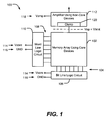
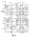
- the data storage cell 226 may be coupled to the first clamp transistor 218 via a selection transistor such as the first MUX transistor 224 to enable a current flow from the voltage supply 206 of the first amplifier 202 through the data storage cell 226, such as illustrated in FIG. 2 .
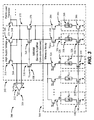
- one of the memory cells 326 may be coupled to the first clamp transistor 318 via a selection transistor such as a respective one of the MUX transistors 324 to enable a current flow from the voltage supply of the first amplifier stage 302 through the corresponding one of the memory cells 326, such as illustrated in FIG. 3 .
Landscapes
- Engineering & Computer Science (AREA)
- Computer Hardware Design (AREA)
- Mram Or Spin Memory Techniques (AREA)
- Hall/Mr Elements (AREA)
Applications Claiming Priority (2)
| Application Number | Priority Date | Filing Date | Title |
|---|---|---|---|
| US12/206,933 US8228714B2 (en) | 2008-09-09 | 2008-09-09 | Memory device for resistance-based memory applications |
| PCT/US2009/055617 WO2010030531A1 (en) | 2008-09-09 | 2009-09-01 | Memory device for resistance-based memory applications |
Publications (2)
| Publication Number | Publication Date |
|---|---|
| EP2332142A1 EP2332142A1 (en) | 2011-06-15 |
| EP2332142B1 true EP2332142B1 (en) | 2013-07-10 |
Family
ID=41226077
Family Applications (1)
| Application Number | Title | Priority Date | Filing Date |
|---|---|---|---|
| EP09792136.5A Active EP2332142B1 (en) | 2008-09-09 | 2009-09-01 | Memory device for resistance-based memory applications |
Country Status (12)
| Country | Link |
|---|---|
| US (1) | US8228714B2 (pt) |
| EP (1) | EP2332142B1 (pt) |
| JP (2) | JP5265773B2 (pt) |
| KR (1) | KR101305337B1 (pt) |
| CN (1) | CN102150214B (pt) |
| BR (1) | BRPI0918916B1 (pt) |
| CA (1) | CA2735725C (pt) |
| ES (1) | ES2424222T3 (pt) |
| MX (1) | MX2011002566A (pt) |
| RU (1) | RU2476940C2 (pt) |
| TW (1) | TWI444998B (pt) |
| WO (1) | WO2010030531A1 (pt) |
Families Citing this family (11)
| Publication number | Priority date | Publication date | Assignee | Title |
|---|---|---|---|---|
| US8228714B2 (en) * | 2008-09-09 | 2012-07-24 | Qualcomm Incorporated | Memory device for resistance-based memory applications |
| KR101094944B1 (ko) * | 2009-12-24 | 2011-12-15 | 주식회사 하이닉스반도체 | 센싱 전압을 제어하는 비휘발성 반도체 집적 회로 |
| US8335101B2 (en) * | 2010-01-21 | 2012-12-18 | Qualcomm Incorporated | Resistance-based memory with reduced voltage input/output device |
| US8625338B2 (en) * | 2010-04-07 | 2014-01-07 | Qualcomm Incorporated | Asymmetric write scheme for magnetic bit cell elements |
| US8254195B2 (en) * | 2010-06-01 | 2012-08-28 | Qualcomm Incorporated | High-speed sensing for resistive memories |
| US8446757B2 (en) | 2010-08-18 | 2013-05-21 | International Business Machines Corporation | Spin-torque transfer magneto-resistive memory architecture |
| US8531902B2 (en) * | 2011-06-30 | 2013-09-10 | Qualcomm Incorporated | Sensing circuit |
| US8693273B2 (en) * | 2012-01-06 | 2014-04-08 | Headway Technologies, Inc. | Reference averaging for MRAM sense amplifiers |
| US10205088B2 (en) * | 2016-10-27 | 2019-02-12 | Tdk Corporation | Magnetic memory |
| US10528862B1 (en) * | 2018-07-26 | 2020-01-07 | Macronix International Co., Ltd. | Neural network system and method for controlling the same |
| US20200098409A1 (en) * | 2018-09-24 | 2020-03-26 | Qualcomm Incorporated | Magnetic random access memory (mram) integration |
Family Cites Families (24)
| Publication number | Priority date | Publication date | Assignee | Title |
|---|---|---|---|---|
| JP2002100181A (ja) * | 2000-09-27 | 2002-04-05 | Nec Corp | 磁気ランダムアクセスメモリ |
| JP3856424B2 (ja) | 2000-12-25 | 2006-12-13 | 株式会社東芝 | 半導体記憶装置 |
| WO2003063312A1 (en) * | 2002-01-21 | 2003-07-31 | Matsushita Electric Industrial Co., Ltd. | Nitride semiconductor laser device and its manufacturing method |
| JP2003223788A (ja) | 2002-01-29 | 2003-08-08 | Hitachi Ltd | 半導体集積回路装置 |
| US6600690B1 (en) * | 2002-06-28 | 2003-07-29 | Motorola, Inc. | Sense amplifier for a memory having at least two distinct resistance states |
| JP3821066B2 (ja) * | 2002-07-04 | 2006-09-13 | 日本電気株式会社 | 磁気ランダムアクセスメモリ |
| JP2004110992A (ja) * | 2002-09-20 | 2004-04-08 | Renesas Technology Corp | 薄膜磁性体記憶装置 |
| US6999345B1 (en) * | 2002-11-06 | 2006-02-14 | Halo Lsi, Inc. | Method of sense and program verify without a reference cell for non-volatile semiconductor memory |
| JP4331966B2 (ja) * | 2003-04-14 | 2009-09-16 | 株式会社ルネサステクノロジ | 半導体集積回路 |
| WO2004095464A1 (ja) * | 2003-04-21 | 2004-11-04 | Nec Corporation | データの読み出し方法が改善された磁気ランダムアクセスメモリ |
| JP4646636B2 (ja) * | 2004-02-20 | 2011-03-09 | ルネサスエレクトロニクス株式会社 | 半導体装置 |
| US7236418B2 (en) * | 2004-06-25 | 2007-06-26 | Qualcomm Incorporated | Reduced area, reduced programming voltage CMOS eFUSE-based scannable non-volatile memory bitcell |
| FR2878067B1 (fr) | 2004-11-17 | 2007-01-26 | St Microelectronics Sa | Dispositif de lecture faible tension notamment pour memoire mram |
| US7082061B2 (en) * | 2004-12-03 | 2006-07-25 | Macronix International Co., Ltd. | Memory array with low power bit line precharge |
| DE102005029872A1 (de) * | 2005-06-27 | 2007-04-19 | Infineon Technologies Ag | Speicherzelle, Lesevorrichtung für die Speicherzelle sowie Speicheranordnungen mit einer derartigen Speicherzelle und Lesevorrichtung |
| US20070015989A1 (en) * | 2005-07-01 | 2007-01-18 | Avantis Medical Systems, Inc. | Endoscope Image Recognition System and Method |
| US7272035B1 (en) | 2005-08-31 | 2007-09-18 | Grandis, Inc. | Current driven switching of magnetic storage cells utilizing spin transfer and magnetic memories using such cells |
| KR100764738B1 (ko) * | 2006-04-06 | 2007-10-09 | 삼성전자주식회사 | 향상된 신뢰성을 갖는 상변화 메모리 장치, 그것의 쓰기방법, 그리고 그것을 포함한 시스템 |
| US7345912B2 (en) * | 2006-06-01 | 2008-03-18 | Grandis, Inc. | Method and system for providing a magnetic memory structure utilizing spin transfer |
| WO2008050398A1 (en) * | 2006-10-24 | 2008-05-02 | Fujitsu Limited | Resistance change memory |
| US20080211541A1 (en) * | 2007-03-02 | 2008-09-04 | Texas Instruments Incorporated | Precision voltage level shifter based on thin gate oxide transistors |
| US7738306B2 (en) * | 2007-12-07 | 2010-06-15 | Etron Technology, Inc. | Method to improve the write speed for memory products |
| US8228714B2 (en) * | 2008-09-09 | 2012-07-24 | Qualcomm Incorporated | Memory device for resistance-based memory applications |
| US8335101B2 (en) * | 2010-01-21 | 2012-12-18 | Qualcomm Incorporated | Resistance-based memory with reduced voltage input/output device |
-
2008
- 2008-09-09 US US12/206,933 patent/US8228714B2/en active Active
-
2009
- 2009-09-01 ES ES09792136T patent/ES2424222T3/es active Active
- 2009-09-01 JP JP2011526135A patent/JP5265773B2/ja active Active
- 2009-09-01 RU RU2011113767/08A patent/RU2476940C2/ru not_active IP Right Cessation
- 2009-09-01 CN CN200980135343.6A patent/CN102150214B/zh active Active
- 2009-09-01 WO PCT/US2009/055617 patent/WO2010030531A1/en not_active Ceased
- 2009-09-01 CA CA2735725A patent/CA2735725C/en not_active Expired - Fee Related
- 2009-09-01 MX MX2011002566A patent/MX2011002566A/es not_active Application Discontinuation
- 2009-09-01 BR BRPI0918916-5A patent/BRPI0918916B1/pt active IP Right Grant
- 2009-09-01 KR KR1020117008148A patent/KR101305337B1/ko active Active
- 2009-09-01 EP EP09792136.5A patent/EP2332142B1/en active Active
- 2009-09-09 TW TW098130422A patent/TWI444998B/zh active
-
2013
- 2013-05-01 JP JP2013096313A patent/JP2013178869A/ja not_active Withdrawn
Also Published As
| Publication number | Publication date |
|---|---|
| CA2735725C (en) | 2014-06-03 |
| JP2013178869A (ja) | 2013-09-09 |
| CA2735725A1 (en) | 2010-03-18 |
| BRPI0918916A2 (pt) | 2018-02-14 |
| KR101305337B1 (ko) | 2013-09-06 |
| RU2476940C2 (ru) | 2013-02-27 |
| RU2011113767A (ru) | 2012-10-20 |
| WO2010030531A1 (en) | 2010-03-18 |
| BRPI0918916B1 (pt) | 2020-07-21 |
| CN102150214B (zh) | 2014-05-07 |
| KR20110053274A (ko) | 2011-05-19 |
| US20100061144A1 (en) | 2010-03-11 |
| TW201023180A (en) | 2010-06-16 |
| TWI444998B (zh) | 2014-07-11 |
| JP5265773B2 (ja) | 2013-08-14 |
| US8228714B2 (en) | 2012-07-24 |
| EP2332142A1 (en) | 2011-06-15 |
| MX2011002566A (es) | 2011-04-07 |
| JP2012502401A (ja) | 2012-01-26 |
| CN102150214A (zh) | 2011-08-10 |
| ES2424222T3 (es) | 2013-09-30 |
Similar Documents
| Publication | Publication Date | Title |
|---|---|---|
| EP2332142B1 (en) | Memory device for resistance-based memory applications | |
| US7272034B1 (en) | Current driven switching of magnetic storage cells utilizing spin transfer and magnetic memories using such cells | |
| US7272035B1 (en) | Current driven switching of magnetic storage cells utilizing spin transfer and magnetic memories using such cells | |
| US7791930B2 (en) | Magnetoresistive random access memory | |
| US10157655B2 (en) | Memory device | |
| CN102148055B (zh) | 使用自旋mos晶体管的非易失性存储器电路 | |
| JP2004103104A (ja) | 薄膜磁性体記憶装置 | |
| US10431277B2 (en) | Memory device | |
| US10269403B2 (en) | Semiconductor storage device | |
| US9472256B1 (en) | Magnetic memory having two transistors and two magnetic tunnel junctions per memory cell | |
| US20070258282A1 (en) | Magnetic memory device and method of writing data in the same | |
| Chang et al. | A low-voltage bulk-drain-driven read scheme for sub-0.5 V 4 Mb 65 nm logic-process compatible embedded resistive RAM (ReRAM) macro | |
| JP5135609B2 (ja) | 半導体装置 | |
| CN113129953A (zh) | 磁性随机存储器的读电路 | |
| US20050052926A1 (en) | Nonvolatile semiconductor memory device | |
| JP2012190515A (ja) | 半導体記憶装置 | |
| JP3884399B2 (ja) | 磁気記憶装置 | |
| JP2010027178A (ja) | 記憶装置 | |
| JP4322048B2 (ja) | 半導体記憶装置 | |
| US11309025B2 (en) | Semiconductor circuit and semiconductor circuit system to suppress disturbance in the semiconductor circuit | |
| JP2004171625A (ja) | 不揮発性記憶装置 | |
| KR101704929B1 (ko) | 센싱 마진을 향상시키는 메모리 셀 읽기 회로 | |
| US20250111869A1 (en) | Memory devices with dual-side access circuits and methods for operating the same | |
| US10832752B2 (en) | Memory write and read assistance using negative differential resistance devices | |
| Takemura et al. | Highly-scalable disruptive reading and restoring scheme for Gb-scale SPRAM and beyond |
Legal Events
| Date | Code | Title | Description |
|---|---|---|---|
| PUAI | Public reference made under article 153(3) epc to a published international application that has entered the european phase |
Free format text: ORIGINAL CODE: 0009012 |
|
| 17P | Request for examination filed |
Effective date: 20110407 |
|
| AK | Designated contracting states |
Kind code of ref document: A1 Designated state(s): AT BE BG CH CY CZ DE DK EE ES FI FR GB GR HR HU IE IS IT LI LT LU LV MC MK MT NL NO PL PT RO SE SI SK SM TR |
|
| AX | Request for extension of the european patent |
Extension state: AL BA RS |
|
| DAX | Request for extension of the european patent (deleted) | ||
| 17Q | First examination report despatched |
Effective date: 20121120 |
|
| GRAP | Despatch of communication of intention to grant a patent |
Free format text: ORIGINAL CODE: EPIDOSNIGR1 |
|
| GRAS | Grant fee paid |
Free format text: ORIGINAL CODE: EPIDOSNIGR3 |
|
| GRAA | (expected) grant |
Free format text: ORIGINAL CODE: 0009210 |
|
| AK | Designated contracting states |
Kind code of ref document: B1 Designated state(s): AT BE BG CH CY CZ DE DK EE ES FI FR GB GR HR HU IE IS IT LI LT LU LV MC MK MT NL NO PL PT RO SE SI SK SM TR |
|
| REG | Reference to a national code |
Ref country code: GB Ref legal event code: FG4D |
|
| REG | Reference to a national code |
Ref country code: AT Ref legal event code: REF Ref document number: 621366 Country of ref document: AT Kind code of ref document: T Effective date: 20130715 Ref country code: CH Ref legal event code: EP |
|
| REG | Reference to a national code |
Ref country code: IE Ref legal event code: FG4D |
|
| REG | Reference to a national code |
Ref country code: DE Ref legal event code: R096 Ref document number: 602009017108 Country of ref document: DE Effective date: 20130912 |
|
| REG | Reference to a national code |
Ref country code: ES Ref legal event code: FG2A Ref document number: 2424222 Country of ref document: ES Kind code of ref document: T3 Effective date: 20130930 |
|
| PG25 | Lapsed in a contracting state [announced via postgrant information from national office to epo] |
Ref country code: SI Free format text: LAPSE BECAUSE OF FAILURE TO SUBMIT A TRANSLATION OF THE DESCRIPTION OR TO PAY THE FEE WITHIN THE PRESCRIBED TIME-LIMIT Effective date: 20130710 |
|
| REG | Reference to a national code |
Ref country code: NL Ref legal event code: T3 |
|
| REG | Reference to a national code |
Ref country code: AT Ref legal event code: MK05 Ref document number: 621366 Country of ref document: AT Kind code of ref document: T Effective date: 20130710 |
|
| REG | Reference to a national code |
Ref country code: LT Ref legal event code: MG4D |
|
| PG25 | Lapsed in a contracting state [announced via postgrant information from national office to epo] |
Ref country code: PT Free format text: LAPSE BECAUSE OF FAILURE TO SUBMIT A TRANSLATION OF THE DESCRIPTION OR TO PAY THE FEE WITHIN THE PRESCRIBED TIME-LIMIT Effective date: 20131111 Ref country code: CY Free format text: LAPSE BECAUSE OF FAILURE TO SUBMIT A TRANSLATION OF THE DESCRIPTION OR TO PAY THE FEE WITHIN THE PRESCRIBED TIME-LIMIT Effective date: 20130717 Ref country code: SE Free format text: LAPSE BECAUSE OF FAILURE TO SUBMIT A TRANSLATION OF THE DESCRIPTION OR TO PAY THE FEE WITHIN THE PRESCRIBED TIME-LIMIT Effective date: 20130710 Ref country code: NO Free format text: LAPSE BECAUSE OF FAILURE TO SUBMIT A TRANSLATION OF THE DESCRIPTION OR TO PAY THE FEE WITHIN THE PRESCRIBED TIME-LIMIT Effective date: 20131010 Ref country code: AT Free format text: LAPSE BECAUSE OF FAILURE TO SUBMIT A TRANSLATION OF THE DESCRIPTION OR TO PAY THE FEE WITHIN THE PRESCRIBED TIME-LIMIT Effective date: 20130710 Ref country code: IS Free format text: LAPSE BECAUSE OF FAILURE TO SUBMIT A TRANSLATION OF THE DESCRIPTION OR TO PAY THE FEE WITHIN THE PRESCRIBED TIME-LIMIT Effective date: 20131110 Ref country code: HR Free format text: LAPSE BECAUSE OF FAILURE TO SUBMIT A TRANSLATION OF THE DESCRIPTION OR TO PAY THE FEE WITHIN THE PRESCRIBED TIME-LIMIT Effective date: 20130710 Ref country code: LT Free format text: LAPSE BECAUSE OF FAILURE TO SUBMIT A TRANSLATION OF THE DESCRIPTION OR TO PAY THE FEE WITHIN THE PRESCRIBED TIME-LIMIT Effective date: 20130710 Ref country code: BE Free format text: LAPSE BECAUSE OF FAILURE TO SUBMIT A TRANSLATION OF THE DESCRIPTION OR TO PAY THE FEE WITHIN THE PRESCRIBED TIME-LIMIT Effective date: 20130710 |
|
| PG25 | Lapsed in a contracting state [announced via postgrant information from national office to epo] |
Ref country code: GR Free format text: LAPSE BECAUSE OF FAILURE TO SUBMIT A TRANSLATION OF THE DESCRIPTION OR TO PAY THE FEE WITHIN THE PRESCRIBED TIME-LIMIT Effective date: 20131011 Ref country code: LV Free format text: LAPSE BECAUSE OF FAILURE TO SUBMIT A TRANSLATION OF THE DESCRIPTION OR TO PAY THE FEE WITHIN THE PRESCRIBED TIME-LIMIT Effective date: 20130710 Ref country code: FI Free format text: LAPSE BECAUSE OF FAILURE TO SUBMIT A TRANSLATION OF THE DESCRIPTION OR TO PAY THE FEE WITHIN THE PRESCRIBED TIME-LIMIT Effective date: 20130710 Ref country code: PL Free format text: LAPSE BECAUSE OF FAILURE TO SUBMIT A TRANSLATION OF THE DESCRIPTION OR TO PAY THE FEE WITHIN THE PRESCRIBED TIME-LIMIT Effective date: 20130710 |
|
| PG25 | Lapsed in a contracting state [announced via postgrant information from national office to epo] |
Ref country code: CY Free format text: LAPSE BECAUSE OF FAILURE TO SUBMIT A TRANSLATION OF THE DESCRIPTION OR TO PAY THE FEE WITHIN THE PRESCRIBED TIME-LIMIT Effective date: 20130710 |
|
| PG25 | Lapsed in a contracting state [announced via postgrant information from national office to epo] |
Ref country code: CZ Free format text: LAPSE BECAUSE OF FAILURE TO SUBMIT A TRANSLATION OF THE DESCRIPTION OR TO PAY THE FEE WITHIN THE PRESCRIBED TIME-LIMIT Effective date: 20130710 Ref country code: RO Free format text: LAPSE BECAUSE OF FAILURE TO SUBMIT A TRANSLATION OF THE DESCRIPTION OR TO PAY THE FEE WITHIN THE PRESCRIBED TIME-LIMIT Effective date: 20130710 Ref country code: MC Free format text: LAPSE BECAUSE OF FAILURE TO SUBMIT A TRANSLATION OF THE DESCRIPTION OR TO PAY THE FEE WITHIN THE PRESCRIBED TIME-LIMIT Effective date: 20130710 Ref country code: DK Free format text: LAPSE BECAUSE OF FAILURE TO SUBMIT A TRANSLATION OF THE DESCRIPTION OR TO PAY THE FEE WITHIN THE PRESCRIBED TIME-LIMIT Effective date: 20130710 Ref country code: EE Free format text: LAPSE BECAUSE OF FAILURE TO SUBMIT A TRANSLATION OF THE DESCRIPTION OR TO PAY THE FEE WITHIN THE PRESCRIBED TIME-LIMIT Effective date: 20130710 Ref country code: SK Free format text: LAPSE BECAUSE OF FAILURE TO SUBMIT A TRANSLATION OF THE DESCRIPTION OR TO PAY THE FEE WITHIN THE PRESCRIBED TIME-LIMIT Effective date: 20130710 |
|
| REG | Reference to a national code |
Ref country code: CH Ref legal event code: PL |
|
| PLBE | No opposition filed within time limit |
Free format text: ORIGINAL CODE: 0009261 |
|
| STAA | Information on the status of an ep patent application or granted ep patent |
Free format text: STATUS: NO OPPOSITION FILED WITHIN TIME LIMIT |
|
| 26N | No opposition filed |
Effective date: 20140411 |
|
| REG | Reference to a national code |
Ref country code: IE Ref legal event code: MM4A |
|
| REG | Reference to a national code |
Ref country code: DE Ref legal event code: R097 Ref document number: 602009017108 Country of ref document: DE Effective date: 20140411 |
|
| PG25 | Lapsed in a contracting state [announced via postgrant information from national office to epo] |
Ref country code: IE Free format text: LAPSE BECAUSE OF NON-PAYMENT OF DUE FEES Effective date: 20130901 Ref country code: LI Free format text: LAPSE BECAUSE OF NON-PAYMENT OF DUE FEES Effective date: 20130930 Ref country code: CH Free format text: LAPSE BECAUSE OF NON-PAYMENT OF DUE FEES Effective date: 20130930 |
|
| PG25 | Lapsed in a contracting state [announced via postgrant information from national office to epo] |
Ref country code: SM Free format text: LAPSE BECAUSE OF FAILURE TO SUBMIT A TRANSLATION OF THE DESCRIPTION OR TO PAY THE FEE WITHIN THE PRESCRIBED TIME-LIMIT Effective date: 20130710 |
|
| PG25 | Lapsed in a contracting state [announced via postgrant information from national office to epo] |
Ref country code: TR Free format text: LAPSE BECAUSE OF FAILURE TO SUBMIT A TRANSLATION OF THE DESCRIPTION OR TO PAY THE FEE WITHIN THE PRESCRIBED TIME-LIMIT Effective date: 20130710 Ref country code: MT Free format text: LAPSE BECAUSE OF FAILURE TO SUBMIT A TRANSLATION OF THE DESCRIPTION OR TO PAY THE FEE WITHIN THE PRESCRIBED TIME-LIMIT Effective date: 20130710 |
|
| PG25 | Lapsed in a contracting state [announced via postgrant information from national office to epo] |
Ref country code: MK Free format text: LAPSE BECAUSE OF FAILURE TO SUBMIT A TRANSLATION OF THE DESCRIPTION OR TO PAY THE FEE WITHIN THE PRESCRIBED TIME-LIMIT Effective date: 20130710 Ref country code: BG Free format text: LAPSE BECAUSE OF FAILURE TO SUBMIT A TRANSLATION OF THE DESCRIPTION OR TO PAY THE FEE WITHIN THE PRESCRIBED TIME-LIMIT Effective date: 20130710 Ref country code: LU Free format text: LAPSE BECAUSE OF NON-PAYMENT OF DUE FEES Effective date: 20130901 Ref country code: HU Free format text: LAPSE BECAUSE OF FAILURE TO SUBMIT A TRANSLATION OF THE DESCRIPTION OR TO PAY THE FEE WITHIN THE PRESCRIBED TIME-LIMIT; INVALID AB INITIO Effective date: 20090901 |
|
| REG | Reference to a national code |
Ref country code: FR Ref legal event code: PLFP Year of fee payment: 8 |
|
| REG | Reference to a national code |
Ref country code: FR Ref legal event code: PLFP Year of fee payment: 9 |
|
| REG | Reference to a national code |
Ref country code: FR Ref legal event code: PLFP Year of fee payment: 10 |
|
| PGFP | Annual fee paid to national office [announced via postgrant information from national office to epo] |
Ref country code: NL Payment date: 20250812 Year of fee payment: 17 |
|
| PGFP | Annual fee paid to national office [announced via postgrant information from national office to epo] |
Ref country code: DE Payment date: 20250808 Year of fee payment: 17 |
|
| PGFP | Annual fee paid to national office [announced via postgrant information from national office to epo] |
Ref country code: IT Payment date: 20250911 Year of fee payment: 17 |
|
| PGFP | Annual fee paid to national office [announced via postgrant information from national office to epo] |
Ref country code: GB Payment date: 20250814 Year of fee payment: 17 |
|
| PGFP | Annual fee paid to national office [announced via postgrant information from national office to epo] |
Ref country code: FR Payment date: 20250808 Year of fee payment: 17 |
|
| PGFP | Annual fee paid to national office [announced via postgrant information from national office to epo] |
Ref country code: ES Payment date: 20251003 Year of fee payment: 17 |