EP2362570B1 - Circuit de communication, réseau de communication et appareil de connexion - Google Patents
Circuit de communication, réseau de communication et appareil de connexion Download PDFInfo
- Publication number
- EP2362570B1 EP2362570B1 EP10015985.4A EP10015985A EP2362570B1 EP 2362570 B1 EP2362570 B1 EP 2362570B1 EP 10015985 A EP10015985 A EP 10015985A EP 2362570 B1 EP2362570 B1 EP 2362570B1
- Authority
- EP
- European Patent Office
- Prior art keywords
- input
- circuit
- signal
- communication
- signals
- Prior art date
- Legal status (The legal status is an assumption and is not a legal conclusion. Google has not performed a legal analysis and makes no representation as to the accuracy of the status listed.)
- Not-in-force
Links
- 230000006854 communication Effects 0.000 title claims description 250
- 238000004891 communication Methods 0.000 title claims description 250
- 230000002950 deficient Effects 0.000 claims description 19
- 238000012544 monitoring process Methods 0.000 claims description 11
- 230000007175 bidirectional communication Effects 0.000 claims description 4
- 238000010586 diagram Methods 0.000 description 16
- 239000000872 buffer Substances 0.000 description 14
- 230000001360 synchronised effect Effects 0.000 description 11
- 238000000034 method Methods 0.000 description 6
- 238000012545 processing Methods 0.000 description 5
- 230000005540 biological transmission Effects 0.000 description 4
- 230000006866 deterioration Effects 0.000 description 4
- 239000002184 metal Substances 0.000 description 4
- 229910052751 metal Inorganic materials 0.000 description 4
- 230000008569 process Effects 0.000 description 4
- 238000007667 floating Methods 0.000 description 3
- 238000004519 manufacturing process Methods 0.000 description 3
- 230000004044 response Effects 0.000 description 3
- 230000008054 signal transmission Effects 0.000 description 3
- RYGMFSIKBFXOCR-UHFFFAOYSA-N Copper Chemical compound [Cu] RYGMFSIKBFXOCR-UHFFFAOYSA-N 0.000 description 2
- 238000006243 chemical reaction Methods 0.000 description 2
- 229910052802 copper Inorganic materials 0.000 description 2
- 239000010949 copper Substances 0.000 description 2
- 238000012423 maintenance Methods 0.000 description 2
- 230000002441 reversible effect Effects 0.000 description 2
- 229910052709 silver Inorganic materials 0.000 description 2
- 239000004332 silver Substances 0.000 description 2
- 230000002457 bidirectional effect Effects 0.000 description 1
- 239000003795 chemical substances by application Substances 0.000 description 1
- 230000000295 complement effect Effects 0.000 description 1
- 239000004020 conductor Substances 0.000 description 1
- 238000012790 confirmation Methods 0.000 description 1
- 230000008878 coupling Effects 0.000 description 1
- 238000010168 coupling process Methods 0.000 description 1
- 238000005859 coupling reaction Methods 0.000 description 1
- 125000004122 cyclic group Chemical group 0.000 description 1
- 238000001514 detection method Methods 0.000 description 1
- 230000000694 effects Effects 0.000 description 1
- 230000002427 irreversible effect Effects 0.000 description 1
- 230000007257 malfunction Effects 0.000 description 1
- 238000012986 modification Methods 0.000 description 1
- 230000004048 modification Effects 0.000 description 1
- 230000009467 reduction Effects 0.000 description 1
- 238000005201 scrubbing Methods 0.000 description 1
- 239000004065 semiconductor Substances 0.000 description 1
- 238000007493 shaping process Methods 0.000 description 1
- 238000012360 testing method Methods 0.000 description 1
Images


Classifications
-
- H—ELECTRICITY
- H04—ELECTRIC COMMUNICATION TECHNIQUE
- H04B—TRANSMISSION
- H04B1/00—Details of transmission systems, not covered by a single one of groups H04B3/00 - H04B13/00; Details of transmission systems not characterised by the medium used for transmission
- H04B1/74—Details of transmission systems, not covered by a single one of groups H04B3/00 - H04B13/00; Details of transmission systems not characterised by the medium used for transmission for increasing reliability, e.g. using redundant or spare channels or apparatus
Definitions
- the present invention relates to a communication circuit, a communication network, and a connecting apparatus. More specifically, the invention relates to the communication circuit, the communication network and the connecting apparatus that enable communication with high reliability.
- error detecting codes such as parity, checksum, cyclic redundancy checksum (CRC) are added to signals, and a check is made whether accurate communication is held by using the error detecting codes. It is requested that reception signals where occurrence of an error is checked are discarded, and signals where an error occurs are retransmitted. However, when signals are retransmitted, communication time of double length is required, and this causes deterioration in a response.
- CRC cyclic redundancy checksum
- Patent Document 1 In recent years, like a computer system disclosed in Japanese Patent No. 3595033 (Patent Document 1), particularly when wiring for communication of important signals is provided, two communication cables are wired so that the same signals are transmitted. Its object is to doubly transmit the same signals and accurately hold communication via any one of the communication cables so as to be capable of communicating even during a failure.
- the double communication using two communication cables enables only the determination whether received signals are properly sent, and when an error cannot be detected by error detecting codes, a determination cannot be made which value is true. For this reason, both signals should be discarded in such a case. In order to complement the discarded signals, retransmission of signals should be demanded, and thus data communication should be again held. For this reason, lengthening of the communication time cannot be avoided. This becomes a problem particularly when immediate response to communicated signals is required, and thus a delay of control occurs.
- two communication circuits should be provided to a transmission side and a reception side, and CPU for comparing the received signals and determining an error is required. That is to say, a part of the processing ability of the CPU is used for determination of an error and selection in communicated signals. Therefore, in order to duplicate signals in conventional systems, special control system and program are required, and this causes complication of a constitution and a rise in manufacturing costs.
- the present invention is devised in view of the above matters, and its object is to provide a communication circuit, a communication network, and a connecting apparatus that can realize communication with very high reliability using a simple wiring system.
- US 2803703 A describes a communication or coupling link having at least three channels.
- a circuit averages outputs of the channels that are approximately in agreement, follows any majority of signals that agree and rejects deviant values, or follows a mean value when all signals disagree.
- US 2004/0199813 A1 refers to a fault-tolerant or self-correcting computer system.
- Three or more processors operate in parallel.
- a controller receives signals from the processor and determines a majority signal value by using a voting logic.
- the controller detects an error when a signal from one of the processors differs from the majority signal.
- a scrubbing module resynchronizes the processors after a predetermined milestone, which may be a predetermined time interval or any other event that may be defined by the user.
- EP 0466224 A1 describes a method and a device for supervising and testing majority voting in a multi-plane digital time selector with essentially identical equipment in each of at least three planes working in parallel. Incoming data is distributed to the planes and passes through the equipment in each of the planes. The outgoing data streams are compared to each other and a majority outgoing data flow based on the comparison is delivered.
- US 6213567 B1 refers to a break system for a motor vehicle and a method for transmitting data in an electrically controlled break system for a motor vehicle.
- the break system includes a pedal unit with one or more sensors detecting the operation of a brake pedal.
- a safety circuit in the pedal unit evaluates the sensor signals according to a majority vote and generates control signals for the brake actuators.
- Data blocks are exchanged over a data bus connecting the pedal unit, the brake actuators, and the central controller.
- An additional signal line connects the pedal unit, the brake actuators, and the central controller for redundantly transmitting the brake application force from the pedal unit to the brake actuators and the central controller. If an irreversible error occurs on the data bus, the additional signal line is used for data transmission.
- a first aspect provides a communication circuit characterized by including a communication line comprising three or more signal lines, a signal distributing section, that is connected to one end of the communication line, for distributing and transmitting a signal input into an input terminal to respective signal lines, and a majority selection receiving circuit, that is connected to the other end of the communication line, for comparing a plurality of reception signals received via the signal lines and selectiving reception signals which are most matched with one another as true so as to output this reception signal to an output terminal.
- the majority selection receiving circuit Since the signal input into the input terminal at one end of the communication line is distributed and transmitted to the respective signal lines by the signal distributing section, the same signals are transmitted to the other end by the signal lines. On the other end, the reception signals received via the signal lines are compared, and the majority selection receiving circuit selectives reception signals which are most matched with one another. For this reason, the same signal as that input into the input terminal on one end is output to the output terminal on the other end. If an error occurs on the reception signal communicated by means of one signal line due to disturbance, this reception signal where the error occurs does not match with the normal reception signals communicated by means of the other two signal lines. However, since the residual two normal reception signals match with each other, the majority selection receiving circuit can select and receive the normal reception signals at real time.
- the signal line is preferably composed of a wire made of metal such as copper or silver with high electric conductivity, and at least three signal lines are provided so that selection according to majority voting can be made.
- the number of signal lines may be four or more, and as the number is increased more and more, the reliability can be further heightened by the majority selection.
- the signal lines are not simply wires, and also coaxial wires having magnetic shield layers on their outsides. As a result, the signal lines are hardly influenced by noises, and this is preferable. Further, the three signal lines may be bundled and be provided with a magnetic shield. It goes without saying that logical signal lines including power line communication and wireless may be formed as the signal lines.
- the signal to be input into the input terminal on one side is a contact input signal that is ON/OFF by switching using an electromagnetic relay or a semiconductor, and for example, when the input terminal is pulled up, the contact input signal in ON state (active state where the signal input is present) is at Low level, and the signal in OFF state (a released state where no signal input is present) is at High level. On the contrary, when the input terminal is pulled down, the contact input signal in ON state is at High level, and the signal in OFF state is at Low level.
- the contact input signal in ON state can be contact input at High/Low level, and in OFF state, the input terminal is at high impedance level (floating level), namely, the signal has three states.
- the signal distributing section may be simply a branch connecting section, but it is preferable that a buffer circuit (shaping/amplifying circuit) for amplifying a voltage or an electric current to be output to the signal lines is provided.
- a buffer circuit shape/amplifying circuit
- the majority selection receiving circuit preferably has a comparator for comparing signals communicated via the signal lines at real time.
- a wire harness is formed with a connector.
- the connector is formed so as to include the signal distributing section formed on one end of the communication line and the majority selection receiving circuit formed on the other end.
- the wire harness can be replaced by the conventional signal cable so as to be used, and the wire harness is easily incorporated into an automatic control system that does not include an arithmetic processing device, so that reliability can be heightened.
- a second aspect provides a communication circuit characterized by including a communication line comprising three or more signal lines, a signal distributing section, that is connected to both ends of the communication line, for distributing and transmitting a signal input into an input/output terminal to the signal lines, a majority selection receiving circuit for comparing a plurality of reception signals received via the signal lines and selectively receiving reception signals which are most matched with one another as true so as to output them to the input/output terminal, and a time division communication control section for switching communication directions of the signal distributing section and the majority selection receiving circuit at time-divided timing so as to hold bidirectional communication.
- the time division communication control section makes a control so that a signal is transmitted from one end to the other end in a state that a signal is input into the one end and input of a signal into the other end is inhibited.
- the time division communication control section makes a control so that a signal is transmitted from the other end to one end in a state that a signal is input into the other end and input of a signal into one end is inhibited.
- the communication direction is switched at the time-divided timing.
- the time division communication control section connected to the ends of the communication line preferably make a synchronous control such that signals are transmitted by the signal distributing section at the ends at synchronous timing such as a token passing system where the signals do not overlap.
- the time division control section spontaneously generates a token call, so that the communication circuit can be allowed to perform a degenerating operation even at the time of disconnecting the communication circuit.
- the signal lines are preferably composed of wires made of metal having high electric conductivity, and as the larger the number of the signal lines is, the higher the reliability can be.
- the signal lines are preferably coaxial wires, and the three signal lines are bundled and a magnetic shield may be provided.
- the signal input into both ends of the communication line is a contact input signal
- the contact input signal is a binary signal that is at High level or Low level in ON state (signal is inputted) and is at opposite level in OFF state.
- the contact input signal is in three states including states that the High and Low signals are input and a state of high-impedance (floating level) at the time of no signal input.
- the signal distributing section may be simply a branch connecting section, but is preferably have a buffer circuit for amplifying a voltage or an electric current to be output to the signal lines.
- the majority selection receiving circuit preferably has a comparator for comparing signals communicated via the signal lines at real time.
- a wire harness is formed by forming connectors including the signal distributing section and the majority selection receiving circuit at both ends of the communication line.
- the wire harness can be replaced by the conventional signal cable so as to be used, and this is easily incorporated into an automatic control system that does not include an arithmetic processing device, so that reliability can be heightened.
- a third aspect provides a communication circuit characterized by including a communication line comprising three or more signal lines, a signal distributing section for distributing parallel signals input into a plurality of input/output terminals at both ends of the communication line, respectively, according to the number of signal lines, and converting the parallel signals into serial signals so as to transmit them to the signal lines, a majority selection receiving circuit for comparing the plurality of serial signals received via the signal lines and selecting serial signals which are most matched with one another as true and converting them into parallel signals so as to output them to the input/output terminals, and a time division communication control section for switching communication directions of the signal distributing section and the majority selection receiving circuit at time-divided timing.
- the time division communication control section preferably makes a synchronous control such as a token passing system at synchronous timing where the signals do not overlap. As a result, collision of signals can be securely prevented.
- the time division control section spontaneously generates a token call, so that the communication circuit can be allowed to perform a degenerating operation even at the time of disconnecting the communication circuit.
- the majority selection receiving section selects and receives the normal reception signals at real time.
- the majority selection receiving section converts the serial signal into the parallel signals before majority selection, and thus more specific real-time communication can be held.
- the majority voting selective reception can be carried out excluding a signal where an error occurs. For this reason, the communication with higher reliability can be held.
- the signal lines are preferably composed of wires made of metal with high electric conductivity, and as the number of the signal lines is larger, the reliability can be further heightened.
- the signal lines are preferably coaxial wires, and the three signal lines may be bundled and a magnetic shield may be provided. It goes without saying that logical signal lines including power line communication and wireless may be formed as the signal lines.
- the signals to be input into both ends of the communication line are preferably contact input signals, and the contact input signals are binary signals that are at High level or Low level in ON state and at an opposite level in Off state. In another way, the contact input signals are preferably in three states including ON states where High and Low signals are input and at a high-impedance level (floating level) in OFF state.
- the signal distributing section may be simply a branch connecting section, but preferably has a buffer circuit for amplifying a voltage or an electric current to be output to the signal lines.
- the majority selection receiving circuit preferably has a comparator for comparing signals communicated via the signal lines at real time.
- the signal distributing section distributes signals to the signal lines after serial conversion, one serial converting section can be provided. However, when parallel signals that are distributed previously according to the number of the signal lines are serially converted, an influence of a defective operation in the serial converting section can be eliminated by the majority selection.
- a wire harness is formed by forming connectors including the signal distributing section and the majority selection receiving circuit, respectively, at both ends of the communication line.
- the wire harness can be replaced by the conventional signal cable so as to be used, and this is easily incorporated into an automatic control system that does not include an arithmetic processing device, so that reliability can be heightened.
- the majority selection receiving circuit has a converting circuit, that are connected to the signal lines, for converting serial signals into parallel signals, a comparing circuit for comparing the plurality of converted parallel signals in unit of parallel signal group, and a selecting circuit for selecting parallel signals which are most matched with one another using the compared result of the comparing circuit.
- the comparing circuit compares the signals parallel-converted by the converting circuit in unit of parallel signal group, the selecting circuit can discriminate properly communicable signals easily and securely.
- the converting circuit, the comparing circuit and the selecting circuit select a reception signal that is the most reliable according to a logical operation, they can select the signal at real time without a delay.
- An input/output circuit for outputting the parallel signals selectively received by the majority selection receiving circuit via the input/output terminals and interlocking the input/output terminal used for outputting the signals so that no signal is input via the input/output terminal is provided.
- the input/output circuit since the input/output circuit interlocks the input/output terminal that outputs a signal so that no signal is input thereinto, the communication direction can be switched according to input signals.
- the communication line is branched and connected on the wiring branching section, and the signal distributing section, the majority selection receiving circuit and the time division communication control section are provided to the terminals of the respective signal lines branched and connected.
- a storage circuit for storing signals received from the terminals of the signal lines branched and connected, and an OR operating circuit for setting a logical sum of the signals at the terminals of the signal lines stored in the storage circuit as a reception signal are provide.
- the reception signal can be received and output also at the terminals of the signal lines branched and connected.
- a logical sum of the signals stored in the storage circuits at the other terminals is output. For this reason, the signal flow direction can be easily and clearly adjusted, and thus the collision of the signals does not occur.
- a plurality of internal signal output sections for outputting the signals received by the majority selection receiving circuit, and a plurality of internal signal input sections for inputting signals transmitted to the signal lines via the signal distributing section, and a grid-shaped wire connecting circuit for connecting the internal signal output section and the internal signal input section arbitrarily so as to switch a connecting state between the input/output terminals are provided.
- the internal signal output sections and the internal signal input sections are connected or disconnected only by switching the connection by means of the grid type wire connecting circuit. For this reason, the wire connecting state between the input/output terminals can be freely set by setting of the grid shaped wire connecting circuit.
- the communication circuit of the present invention is a wire harness where the relay connecting section is formed in a relay connector provided to a relay end, the wire harnesses are easily connected to each other so as to form a network.
- a fourth aspect provides a communication network formed by connecting a plurality of communication circuits into a netlike pattern via the grid-shaped connecting circuit.
- the grid-shaped wire connecting circuit comprises a programmable logic device, and the internal signal output section has a writing port for writing wire connecting information, and the majority selection receiving circuit has a reliability monitoring circuit for counting how many times defective communication occurs and/or how many times proper reception cannot be carried out so as to obtain reliability of the signal lines.
- the communication network has a wire connection adjusting section for adjusting wire connecting states obtained by the grid-shaped wire connecting circuits so that the communication lines with low reliability are bypassed on positions where the reliability monitoring circuits and the writing port of every communication circuit are communicable.
- the communication network according to the present invention is formed by connecting a plurality of communication lines into a netlike pattern, a signal input into one input/output terminal on the communication network is transmitted via the plurality of communication lines, and is output into the input-output terminal provided on another communication circuit connected by the grid-shaped wire connecting circuit.
- the grid-shaped wire connecting circuit comprises the programmable logic device such as FPGA, the wire connecting state can be adjusted dynamically by the wire connection adjusting section. Since the majority selection receiving circuit has the reliability monitoring circuit, when a determination is made that the reliability of the communication circuit is low due to various noises and deteriorations, the wire connecting state of the grid-shaped wire connecting circuit can be changed dynamically without this communication circuit.
- the plurality of communication circuits can hold communication according to the majority selection of higher reliability, and also when defective communication due to disconnection or characteristic deterioration that cannot be avoided occurs on one communication circuit, the signals can be transmitted so as to bypass the communication circuit where the defective communication occurs. As a result, the communication with higher reliability can be held. It is more preferable that when the signal distributing sections connected to the communication circuits, respectively, generate token calls actively so as to hold degenerating communication at the time of disconnecting the signal lines.
- the communication network that holds the communication with higher reliability is suitable for wiring on a portion requiring high reliability in automatic control devices to be incorporated into transporting means such as an automobile, an airplane, a ship and a rocket, and devices such as robot.
- a fifth aspect provides a connecting apparatus characterized by including relay input/output terminals connected to input/output terminals of at least two communication circuits, internal signal output sections for outputting signals received from every relay input/output terminal, internal signal input sections for inputting the signals transmitted from every relay input/output terminals, an input/output circuit for outputting parallel signals input into the internal signal input sections via the relay input/output terminals and interlocking to prevent input of another signal via the relay input/output terminal outputting the signals, and simultaneously outputting the signals input via the relay input/output terminals via the internal signal output sections, and a grid-shaped wire connecting circuit for connecting the internal signal output sections and the internal signal input sections arbitrarily so as to switch a connecting state between the input/output terminals.
- the connecting apparatus of the present invention connects the input/output terminals of the at least two communication circuits to the relay input/output terminals so as to relay the signal input into any input/output terminal in one communication circuit so as to be capable of outputting the signal to the input/output terminal of another communication circuit. That is to say, the signal input into the input/output terminal of one communication circuit is output to the internal signal output section to which this is connected, and this signal is input into the internal signal input section via the grid-shaped wire connecting circuit so as to be capable of relaying it to another communication circuit.
- the connecting apparatus becomes a repeater of the wire harness. Further, when the relay input/output terminals are provided so that the three or more communication circuits can be connected to one connecting apparatus, the connecting apparatus becomes a branch connecting apparatus of the communication circuits.
- the grid-shaped wire connecting circuit comprises the programmable logic device, and a writing port for writing wire connecting information into the programmable logic device so as to enable the wire connecting state by means of the grid-shaped wire connecting circuit to be adjustable is provided.
- the relay of signals by means of the connecting apparatus can be dynamically changed. That is to say, while the communication circuit with low reliability is operating, this circuit can be dynamically bypassed easily.
- the writing port is provided to internal signal output section, so that contents to be output to the writing port can be transmitted by communication.
- the communication circuits from the first to third aspects allow the same signals to communicate using the three or more signal lines, and can eliminate an influence of disturbance in unit of communication circuit at real time by means of majority selection. That is to say, a good balance can be achieved between a high-speed response and high reliability.
- the communication circuit of the present invention can be replaced by a conventional communication circuit so as to be used, in order to secure the conventional high reliability, the on/off contact signal can be transmitted without a CPU that is comparatively expensive and causes a defective operation and a delay of a process.
- a signal to be input/output to the input/output terminals can be shared on two or more separated positions.
- the communication network from the fourth aspect is formed by using a plurality of communication circuits, so that the reliability of the communication can be further heightened.
- the connecting apparatus from the fifth aspect can relay and connect or branch and connect a plurality of communication circuits easily.
- FIGS. 1 and 2 are diagrams describing a configuration of a communication circuit 1 according to a first embodiment of the present invention.
- the communication circuit 1 has a communication line 2, a signal distributing section 4, and a majority selection receiving circuit 5.
- the communication line 2 comprises three signal lines 2a, 2b and 2c.
- the signal distributing section 4 is connected to one end of the communication line 2, and distributes and transmits a signal input into an input terminal 3i to the signal lines 2a, 2b and 2c.
- the majority selection receiving circuit 5 is connected to the other end of the communication line 2, and compares a plurality of reception signals received via the signal lines 2a, 2b and 2c so as to selectively receive the reception signals which are most matched with one another as true and output them to an output terminal 3o.
- a connector 6 houses the input terminal 3i and the signal distributing section 4, and a connector 7 houses the majority selection receiving circuit 5 and the output terminal 3o.
- the communication circuit 1 of the present invention is a wire harness that can connect a control target 8 (e.g. a motor M or the like) to a control device 9.
- the control target 8 and the control device 9 have connectors 8a and 9a connectable to the wire harness 1, and the connectors 6 and 7 of the wire harness 1 can be connected to the connectors 8a and 9a.
- the signal lines 2a, 2b and 2c are coaxial cables having magnetic shields 2s made of mesh-shaped conductors, and these magnetic shields 2s are connected to grounds of the signal distributing section 4 and the majority selection receiving circuit 5.
- the communication circuit 1 of the present invention may have three or more signal lines 2a, 2b and the like.
- the input terminal 3i and the output terminal 3o form connecting terminals of the connectors 6 and 7, and are made of plugs or receptacles.
- one terminal is provided to each of the connectors 6 and 7.
- the signal distributing section 4 has a plurality of buffers 4a, 4b and 4c according to the number of signal lines 2a, 2b and 2c, and these buffers 4a, 4b and 4c solve insufficient electric current due to branching of a signal in a branching section 4d.
- the majority selection receiving circuit 5 has comparators 5a, 5b and 5c and a selecting circuit 5d.
- the comparators 5a, 5b and 5c compare two of reception signals received via the signal lines 2a, 2b and 2c.
- the selecting circuit 5d selects reception signals which are most matched with one another based on the compared result in the comparators 5a, 5b and 5c.
- a hardware process enables majority selection receiving.
- the communication circuit 1 having the above configuration is replaced by the wire harness used as a normal communication line, so that the signals can be transmitted to a direction of arrow X and reliability of the communication can be greatly heightened.
- the magnetic shields 2s absorb most of the noise N. That is to say, the three signals received via the three signal lines 2a, 2b and 2c are the same, and all the comparators 5a, 5b and 5c output matching.
- the selecting circuit 5d may receive a signal from any of the signal lines 2a, 2b and 2c, and may select any signal as a true value.
- the selecting circuit 5d selects any one of the matched signals received via the signal lines 2b and 2c so as to output the selected signal to the output terminal 3o.
- the communication circuit 1 of the present invention can be used for a portion requiring high reliability in a simpler automatic control system as exemplified in the first embodiment.
- the coaxial cables are adopted as the signal lines 2a, 2b and 2c, the influence of the external noise N is hardly exerted, but these signal lines 2a, 2b and 2c may be electric wires made of metal such as copper or silver.
- these signal lines 2a, 2b and 2c may be electric wires made of metal such as copper or silver.
- one input terminal 3i and one output terminal 3o are provided to one connector 6 and one connector 7, respectively, signals are continuously transmitted without changing over a switch.
- a plurality of input terminals 3i and output terminals 3o can be transmitted by time-division serial communication.
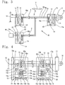
- FIGS. 3 and 4 are diagrams illustrating a configuration of the communication circuit 10 according to a second embodiment.
- the members having the same reference symbols as those in FIGS. 1 and 2 are the same as or equivalent to members in FIGS. 1 and 2 , detailed description thereof is omitted so that the overlapped description is avoided.
- the communication circuit 10 has the communication line 2, signal distributing sections 12, majority selection receiving circuits 13, time division communication control sections 14, and output circuits 15.
- the communication line 2 comprises three or more signal lines 2a, 2b and 2c.
- the signal distributing section 12 is connected to a terminal of the communication line 2, distributes and transmits a signal input into an input/output terminal 11 to the signal lines 2a, 2b and 2c.
- the majority selection receiving circuit 13 compares a plurality of reception signals received via the signal lines 2a, 2b and 2c, and selectively receives the reception signals which are most matched with one another as true so as to output the signals to the input/output terminal 11.
- the time division communication control section 14 switches communication directions of the signal distributing section 12 and the majority selection receiving circuit 13 at time-divided timing so as to hold bidirectional communication.
- the input/output circuit 15 outputs the signal selectively received by the majority selection receiving circuit 13, and when outputting the signal, interlocks so as not to input a signal.
- a wiring branching section 2e is provided to the communication line 2.
- the communication line 2 Since in the communication circuit 10 according to the second embodiment, the communication line 2 is branched and connected by the wiring branching section 2e, the communication line 2 has three terminals.
- the communication circuit 10 is a wire harness where connectors 10a to 10c are provided to the terminals, respectively.
- a number of branching of the communication line 2 is determined by a number of devices that output control signals for controlling the motor 16.
- the second embodiment describes an example where the communication line 2 has the three terminals in order to simplify the description, but it goes without saying that the number of branching can be adjusted freely if necessary.
- the input/output terminals 11 form connecting terminals of the connectors 10a to 10c, respectively, and the input/output terminals 11 of the communication line are made of plugs or receptacles, and the second embodiment describes an example where one input/output terminal is provided to each of the connectors 10a to 10c in order to simplify the description.
- signals input into the input/output terminals 11 by the signal distributing sections 12 are converted into serial signals so as to be capable of being transmitted in time division.
- the signal distributing section 12 outputs input signals from input/output terminals 11 as any one of ON signals at High level and Low level, and an OFF signal of high impedance (three-state signals) to the signal lines 2a, 2b and 2c at timing determined by the time division communication control section 14.
- signal distributing section 12 has three-state buffers 12a, 12b and 12c provided according to the number of signal lines 2a, 2b and 2c.
- a voltage level of the three-state buffers 12a, 12b and 12c at the time of high impedance is set to be a voltage level between the High level and the Low level (hereinafter, a Mid level).
- the majority selection receiving circuit 13 has comparators 13a, 13b and 13c that compares two of reception signals received via the signal lines 2a, 2b and 2c, and a selecting circuit 13d that selects reception signals which are most matched with one another by using a comparison result from the comparators 13a, 13b and 13c.
- the majority selection receiving circuit 13 enables majority selection receiving according to a hardware process.
- the time division communication control section 14 is for holding synchronous communication using a token passing system, and has a token call control section 14a, an SS (Sending Slot) storage section 14b, an RS (Receiving Slot) storage section 14c, a signal transmission control section 14d and a signal reception control section 14e.
- the token call control section 14a has an arbitration function for positively sending a token signal.
- the SS storage section 14b stores a node number of a self station.
- the RS storage section 14c records a node number of reception station.
- the signal transmission control section 14d outputs a signal to the signal distributing section 12 according to a synchronous timing at which the self station node recorded in the SS storage section 14b is allocated by the token signal.
- the signal reception control section 14e allows the majority selection receiving circuit 13 to receive signals from multi-station nodes stored in the RS storage section 14c.
- the input/output circuit 15 connects the input/output terminal 11 to the signal distributing section 12 or the majority selection receiving circuit 13 in a switching manner, and thus interlocks so as not to input a signal from the input/output terminal 11 into the signal distributing section 12 when the signal from the majority selection receiving circuit 13 is output to the input/output terminal 11.
- the input/output circuit 15 has a storage circuit 15a, a OR operating circuit 15b, and a switching circuit 15c.
- the storage circuit 15a once stores an ON/OFF state and voltage level of reception signals from multi-nodes recorded in the RS storage section 14c for one or more token cycle.
- the OR operating circuit 15b operates a logical sum in a state that the signals stored in the storage circuit 15a are in ON state, and obtains a license of the communication line 2.
- the switching circuit 15c changes over the switch so that when any one of the reception signals from the multi-nodes recorded into the RS storage section 14c proves to be in ON state by the logical OR operation of the OR operating circuit 15b, a voltage level of the reception signal is output to the input/output terminal 11.
- a motor 16 locks and unlocks doors of an automobile, and a motor driver 17 supplies an electric power to the motor 16.
- An operation switch 18 locks/unlocks the doors according to a user's input operation, and an electronic control unit 19 sends a control signal to the motor driver 17 according to remote control by means of an electromagnetic wave.
- the motor driver 17, the operation switch 18 and the electronic control unit 19 have connectors 17a, 18a and 19a, respectively.
- the connectors 17a, 18a and 19a are connected to the connectors 10a, 10b and 10c of the communication circuit 10, respectively, so that the respective members 17, 18 and 19 are connected to each other by a wiring system of the communication circuit 10.
- each of the token call control sections 14a at each of the nodes actively generates a call.
- the timing at which token is called is shifted according to the information stored in the SS storage sections 14b, and thus the token call control section 14a at the node with SS number "1" with the highest priority (the input/output terminal 11 of the connector 10a to which the operation switch 18 is installed) is selected as a bus master so as to call tokens T1 to T3 and determine entire synchronous timing.
- the token call control section 14a since three nodes are present in the communication circuit 10, the token call control section 14a generates the tokens T1 to T3 according to its number at each predetermined time (slot cycle) T.
- the respective nodes transmit to the communication line 2 the self node numbers "#1" to "#3" and the signals input into the input/output terminals 11 at the synchronous timings given to the self stations.
- a Mid level (OFF state) is transmitted.
- Waveforms S1 to S3 shown in FIG. 5 represent signals to be transmitted to the communication line 2 by the signal distributing sections 12 in the connectors 10a to 10c, and one example is described with reference to a solid line, and a fluctuation range of the signal is shown by a dotted line.
- SW represents an input signal from the operation switch 18, and Mot represents an output signal to the motor driver 17.
- the signal distributing section 12 in the connector 10a transmits the self station node number "#1" and then a High level to the communication line 2 according to an input signal.
- the majority selection receiving circuit 13 in the connector 10b receives this signal and outputs it to the input/output terminal 11. That is to say, when the High level is output to the motor driver 17 and a driving current is applied to the motor 16, the motor 16 rotates to a regular direction.
- the motor 16 rotates in a reverse direction. That is to say, the motor 16 is rotated to the regular and reverse directions by the switch SW so that an automobile can be locked or unlocked.
- the reception of the High-level signal from the node "1" is stored in the storage circuits 15a provided to the input/output circuits 15 at the nodes with numbers "2" and "3", and the received voltage signal at High level is output to the input/output terminals 11.
- the OR operating circuits 15b detect a node from which an ON signal is input into the storage circuits 15a, and the switching circuit 15c is switched to interlock and prevent the signal input from the input-terminal 11.
- a contact input signal input into the input/output terminal 11 with the node number "1" is output directly to the input/output terminals 11 with the node numbers "2" and "3".
- the input/output terminals 11 in the connectors 10a to 10c are connected directly by the communication line in a pseudo manner.
- the contact input signal can communicate bidirectionally as shown by a bidirectional arrow Y in FIG. 3 , but the interlocking is given by the input/output circuit 15, so that collision of signals is prevented even when conflicting input is performed at both ends of the communication circuit 10. This is an effect that can be obtained because the communication circuit 10 holds the synchronous communication.
- the second embodiment describes the example where when a three-state buffer is used in the second embodiment, two voltages (High level and Low level) in ON state and an intermediate voltage (Mid level) in OFF state might be generated as the signals to be transmitted to the signal lines 2a to 2c.
- the present invention is not limited to it. That is to say, a signal for identifying a 2-bit binary value that is a signal for identifying two ON states (High level and Low level), and a signal for identifying ON state or OFF state may be transmitted separately to the signal lines 2a to 2c.
- the buffers to be used for the signal transmission open-collector type buffers are used in order to close to characteristics of a common bus, or power line communication or wireless communication are used. It goes without saying that such various modification can be considered.
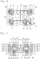
- FIGS. 6 and 7 are diagrams illustrating configurations of the communication circuit 20 according to a third embodiment of the present invention.
- the members denoted by the same reference symbols as those in FIGS. 1 to 5 are the same as or equivalents to those in FIGS. 1 to 5 , detailed description thereof is omitted to avoid overlapped description.
- the communication circuit 20 has the communication line 2, signal distributing sections 21, majority selection receiving circuits 22, the input/output circuits 15, and the time division communication control sections 14.
- the communication line 2 comprises three signal lines 2a to 2c.
- the signal distributing section 21 distributes parallel signals input into the plurality of input/output terminals 11 (11a to 11h) at both ends of the communication line 2 according to the number of the signal lines 2a to 2c and converts these signals into serial signals so as to transmit them to the signal lines 2a to 2c.
- the majority selection receiving circuit 22 compares the plurality of serial signals received via the signal lines 2a to 2c, and selects serial signals which are most matched with one another as true so as to convert them into parallel signals.
- the input/output circuit 15 outputs the parallel signals selectively received by the majority selection receiving circuit 22 via the input/output terminals 11 and interlocks to prevent the signal via the input/output terminal 11 that outputs a signal.
- the time division communication control section 14 switches the communication direction among the signal distributing section 21, the majority selection receiving circuit 22 and the input/output circuit 15 at time-divided timing.
- a wire connection setting section 23 is branched and connected to the communication line 2 composing the communication circuit 20.
- the wire connection setting section 23 has a plurality of internal signal output sections 24, a plurality of internal signal input sections 25, a grid-shaped wire connecting circuit 26, and a relay connecting section 27.
- the internal signal output sections 24 output signals received by the majority selection receiving circuit 22, respectively.
- the internal signal input sections 25 input the signals to be transmitted to the communication line via the signal distributing section 21, respectively.
- the grid-shape wire connecting circuit 26 connects any internal signal output section 24 and any internal signal input section 25 so as to switch the connecting state between the input/output terminals 11.
- the relay connecting section 27 is connected to the grid-shape wire connecting circuit 26, and connects another communication circuit 20' so as to relay signals between the communication circuits 20 and 20'.
- 28a to 28c denote electronic circuits and devices to be controlled that automatically control ECU (Electric Control Unit) and the like to be connected to the plurality of input/output terminals 11.
- the signal distributing section 21 according to the third embodiment is basically the same as the signal distributing sections 4 and 12 described in the first and second embodiments, but is different from them in that a converting circuit 21d for converting parallel signals into serial signals is provided before buffers 21a to 21c for distributing and outputting signals to the signal lines 2a to 2c.
- the buffers 21a to 21c output binary signals that are in ON state at Low level and in OFF state at High level. Therefore, the buffers 21a to 21c do not have to be three-state buffers.
- An input signal is first branched, a plurality of converting circuits 21d whose number is according to the number of signal lines 2a to 2c is provided. As a result, defective communication caused by a defective operation of the converting circuit 21d may be enabled to be eliminated by the majority selection receiving.
- the majority selection receiving circuit 22 is approximately the same as the majority selection receiving circuits 5 and 13, but they are different in that converting circuits 22d to 22f for converting serial signals into parallel signals are provided between comparators 22a to 22c and the signal lines 2a to 2c. Also in this case, after the converting circuits 22d to 22f are first used to parallel-convert signals, the comparators 22a to 22c compare the signals, and the selecting circuit 22g makes the majority selection. For this reason, defective communication caused by a defective operation of the converting circuits 22d to 22f can be also eliminated by the majority selection.
- the input/output circuit 15 Since the input/output circuit 15 according to the third embodiment inputs/outputs a contact signal that is at a Low level in ON state, its control circuit can be formed by a simple switching element.
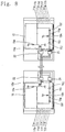
- FIG. 8 is a diagram illustrating one example of the input/output circuit 15 using a switching element.
- a switching element 15d such as FET is connected to the majority selection receiving circuit 22, and a pull-up resistor 15e is connected between the switching element 15d and a power supply Vcc.
- a diode 15f is connected to the switching element 15, the resistor 15e and the input/output terminal 11a, and resistors 15g and 15h are connected to the diode 15f in series.
- a diode 15i is connected between the resistors 15g and 15h and the power supply Vcc.
- a logical inverting circuit 15j is connected to the resistor 15h.
- a circuit formed by a series of elements 15d to 15j inverts a signal received by the majority selection receiving circuit 22 to output it to the input/output terminal 11a.
- the majority selection receiving circuit 22 When the majority selection receiving circuit 22 is in ON state (High level), the circuit outputs the signal at Low level via the input/output terminal 11a, and interlocks to prevent input of a signal via the input/output terminal 11a. That is to say, only when an output signal from the majority selection receiving circuit 22 is in OFF state (Low level), a voltage at an input end of the logical inverting circuit 15j changes according to the voltage level of the input/output terminal 11a, and the inverted signal is input into the signal distributing section 21.
- the communication circuit 20 With the provision of the input/output circuit 15, the communication circuit 20 enables the bidirectional communication according to the input signal into the input/output terminals 11a to 11h.
- a circuit is configured by simply combining elements such as diodes and transistors that perform simple operations.
- a complicated control circuit such as CPU is eliminated. As a result, the manufacturing cost can be reduced, and also occurrence of malfunctions can be prevented more securely.
- FIG. 8 illustrates only a main section in order to describe the part of the circuit configuration where the input signal is interlocked in detail. For this reason, it goes without saying that the description about various detailed members included in the communication circuit 20 are omitted.
- the wire connection setting section 23 sets connection of wires selected arbitrarily from the input/output terminals 11, the internal signal output section 24 is an output port that outputs the same signal as that to be output to the input/output terminal 11 selected in advance, and the internal signal input section 25 is an input port that inputs the signal to be output to the input/output terminal 11.
- the grid-shaped wire connecting circuit 26 wire connecting lines connected to the internal signal input sections 25 and the internal signal output sections 24 are arranged into a grid pattern and are placed on positions where the wires are desired to be connected, and the wire connecting lines are connected.
- the grid-shaped wire connecting circuit 26 can be easily formed by a programmable logic device.
- a reliability monitoring circuit 22h is provided to the majority selection receiving circuit 22, and counts how many times defective communication occurs and/or how many times proper reception cannot be carried out so as to obtain reliability of the communication lines.
- a writing port 24a is provided to the internal signal output section 24, and writes information about the wire connection into the programmable logic device.
- a wire connection adjusting section 29 adjusts a state of the wire connection by mean of the respective grid-shaped wire connecting circuit 26 so that communication wires with low reliability are bypassed on positions communicable with the reliability monitoring circuit 22h and the writing port 24a of the communication circuits 20 and 20' .
- the reliability of signals is secured, and the parallel signals comprising a lot of ON/OFF signals can communicate using only three signal lines. For this reason, the number of wirings is reduced, and thus simple wiring with less error can be carried out. Since the wire connecting state can be changed by the grid-shaped wire connecting circuit 26 and the hard constitution does not have to be changed, the maintenance can be done easily.
- the communication circuit 20 can connect a lot of ECUs like connection using a flat cable.
- the reliability monitoring circuit 22h records a number of times of avoiding defective communication and a number of unavoidable times according to the majority selection so as to check the reliability of the communication circuit 20. For this reason, the wire connection adjusting section 29 can rewrite the wire connection information about the programmable logic device via the writing port 24a so that the communication circuit 20 with low reliability is bypassed. That is to say, the communication circuits 20 and 20' can be dynamically sorted out. The multiplexing in unit of the communication circuit 20 and 20' is realized, thereby securing higher reliability.
- FIG. 9 is a diagram illustrating a constitution of a wire connecting device 30 constituted so as to be capable of connecting the communication circuits 10, 20 and 20'.
- the connecting device 30 has relay input/output terminals 31a and 31b, internal signal output section 32a and 32b, internal signal input sections 33a and 33b, input/output circuits 34a and 34b, and a grid-shaped wire connecting circuit 35.
- the relay input/output terminals 31a and 31b are connected to the at least two input/output terminals 11a and 11b of the communication circuits 10 and 20 and 20'.
- the internal signal output sections 32a and 32b output signals received from the relay input/output terminals 31a and 31b, respectively.
- the internal signal input sections 33a and 33b input the signals transmitted from the relay input/output terminals 31a and 31b, respectively.
- the input/output circuits 34a and 34b output parallel signals input into the internal signal input sections 33a and 33b via the relay input/output terminals 31a and 31b and interlock to prevent signals from being input via the relay input/output terminals 31a and 31b, and simultaneously output signals input via the relay input/output terminals via the internal signal output sections.
- the grid-shaped wire connecting circuit 35 arbitrarily connects the internal signal output section 32a and 32b and the internal signal input section 33a and 33b so as to switch the connecting state of the input/output terminals 31a and 31b.
- the relay input/output terminals 31a and 31b have the approximately same configuration as those of the input/output terminals 11, and are connectable to the input/output terminals 11 of the communication circuits 10, 20 and 20' to be connected.
- the relay input/output terminals 31a and 31b are provided in two direction, but it goes without saying that a number and directions of the relay input/output terminals 31a and 31b to be provided can be arbitrarily set.
- the internal signal output sections 32a and 32b and the internal signal input sections 33a and 33b are the same as the internal signal output sections 24 and the internal signal input sections 25 shown in FIG. 6 . For this reason, detailed description of the constitutions is omitted.
- a writing port 32c is formed on any one of the internal signal output sections 32a and 32b.
- the grid-shaped wire connecting circuit 35 is formed by the programmable logic device, and the wire connection information is written into the programmable logic device via the writing port 32c, so that the wire connecting state can be changed.
- the connecting device composes a connecting adaptor of the wire harness, and this can form any communication network.
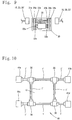
- FIG. 10 is a diagram illustrating one example of a communication network 40 formed by using the connecting device 30.
- the communication network 40 according to the third embodiment is an example where wire harnesses 1' formed by any one of the communication circuits 10, 20 and 20' are connected into a net shape via the connecting devices 30. Since ECUs 41a to 41d to be connected in the example are connected to by two routes, if one wire harness 1' is completely disconnected at a portion C and the communication is disabled, the reliability monitoring circuit 22h (see FIG. 6 ) provided to both ends of the wire harness 1' that cannot communicate detects the disconnection of the wire harness 1'. Further, the wire connection adjusting section 29 adjusts the wire connecting state. As a result, this network can dynamically cope with a communicable environment that is the same as that before the disconnection of the wire harness 1'.
- the constitution that is as simple as possible is illustrated in order to simplify the description, but it goes without saying that the communication network 40 can be actually structured in order to secure three or more routes between important ECUs.
Landscapes
- Engineering & Computer Science (AREA)
- Computer Networks & Wireless Communication (AREA)
- Signal Processing (AREA)
- Cable Transmission Systems, Equalization Of Radio And Reduction Of Echo (AREA)
- Detection And Prevention Of Errors In Transmission (AREA)
- Bidirectional Digital Transmission (AREA)
- Logic Circuits (AREA)
- Small-Scale Networks (AREA)
Claims (10)
- Circuit de communication comprenant
une ligne de communication (2) qui comprend trois, ou plus, lignes de signaux (2a, 2b, 2c) par lesquelles plusieurs noeuds (17, 18, 19) sont connectés entre eux, des sections de répartition de signaux (12, 21) qui sont connectées aux extrémités de la ligne de communication (2), pour répartir et transmettre aux lignes de signaux respectives (2a, 2b, 2c) des signaux entrés dans des bornes d'entrée/sortie (11) à partir des noeuds (17, 18, 19),
des circuits de réception de sélection de majorité (13, 22) pour comparer plusieurs signaux de réception reçus par l'intermédiaire des lignes de signaux (2a, 2b, 2c) et sélectionner comme corrects les signaux de réception qui concordent le plus, de manière à les sortir vers une borne d'entrée/sortie respective,
et caractérisé par
des sections de commande d'appels jetons (14a) pour transmettre des appels jetons en fonction d'un nombre de noeuds respectifs, parmi l'ensemble de noeuds, à un moment prédéterminé, et
des sections de commande de communication à répartition dans le temps (14) pour changer les directions de communication des sections de répartition de signaux (12, 21) et des circuits de réception de sélection de majorité (13, 22) à un rythme réparti dans le temps, de manière à permettre une communication bidirectionnelle, grâce à la sortie par un noeud prédéterminé d'un signal entré dans une borne d'entrée/sortie (11) par le noeud prédéterminé, à un moment de l'appel jeton du noeud prédéterminé, et conçues pour verrouiller mutuellement un noeud autre que le noeud prédéterminé afin d'empêcher un signal d'être entré à partir de l'autre noeud dans une borne d'entrée/sortie respective (11). - Circuit de communication selon la revendication 1, comprenant également un circuit d'entrée/sortie (15) qui contient un circuit de commutation (15c) pour modifier les directions de communication commandées par la section de commande de communication à répartition dans le temps (14), le circuit d'entrée/sortie (15) connectant par commutation la borne d'entrée/sortie (11) à la section de répartition de signaux (12, 21) ou au circuit de réception de sélection de majorité (13, 22), de sorte que lorsque le signal provenant du circuit de réception de sélection de majorité (13, 22) est sorti vers la borne d'entrée/sortie (11), le verrouillage est prévu en ne permettant pas au signal provenant de la borne d'entrée/sortie (11) d'être entré dans la section de répartition de signaux (12, 21).
- Circuit de communication selon la revendication 1 ou 2, dans lequel
la section de répartition de signaux (21) répartit des signaux parallèles entrés dans plusieurs bornes d'entrée/sortie (11) aux deux extrémités de la ligne de communication (2), respectivement, selon le nombre de lignes de signaux (2a, 2b, 2c), et convertit les signaux parallèles en signaux série, de manière à les transmettre aux lignes de signaux (2a, 2b, 2c), et le circuit de réception de sélection de majorité (22) compare les signaux série reçus par l'intermédiaire des lignes de signaux (2a, 2b, 2c) et sélectionne comme corrects les signaux série qui concordent le plus, et les convertit en signaux parallèles, de manière à les sortir vers les bornes d'entrée/sortie (11) . - Circuit de communication selon la revendication 3, dans lequel
le circuit de réception de sélection de majorité (22) comporte
un circuit de conversion (22d-f), qui est connecté aux lignes de signaux (2a, 2b, 2c), pour convertir les signaux série en signaux parallèles,
un circuit de comparaison pour comparer les signaux parallèles convertis, dans une unité de groupe de signaux parallèles, et
un circuit de sélection (22g) pour sélectionner comme corrects les signaux parallèles qui concordent le plus, à l'aide du résultat comparé du circuit de comparaison. - Circuit de communication selon l'une des revendications 1 à 4, dans lequel
la ligne de communication (2) est branchée et connectée sur la section de branchement de câblage, et la section de répartition de signaux (21), le circuit de réception de sélection de majorité (22) et la section de commande de communication de division dans le temps (14) sont prévus sur les bornes des lignes de signaux respectives (2a, 2b, 2c) branchées et connectées, et il est prévu par ailleurs
un circuit de stockage (15a) pour le stockage des signaux par la sélection de majorité reçue à partir des bornes des lignes de signaux (2a, 2b, 2c) branchées et connectées, et
un circuit d'opération OU pour fixer une somme logique des signaux aux bornes des lignes de signaux (2a, 2b, 2c) stockés dans le circuit de stockage (15a) comme signal de réception. - Circuit de communication selon l'une des revendications 1 à 5, dans lequel il est prévu
plusieurs sections de sortie de signaux internes (24) pour la sortie des signaux par la sélection de majorité reçue par le circuit de réception de sélection de majorité (22), et
plusieurs sections d'entrée de signaux internes (25) pour l'entrée de signaux transmis aux lignes de signaux (2a, 2b, 2c) par l'intermédiaire de la section de répartition de signaux (21), et
un circuit de connexion de fils en forme de grille (26) pour connecter la section de sortie de signaux internes (24) et la section d'entrée de signaux internes (25) arbitrairement de manière à commuter un état de connexion entre les bornes d'entrée/sortie (11). - Circuit de communication selon la revendication 6, dans lequel il est prévu une section de connexion de relais (27) qui est connectée directement au circuit de connexion de fils en forme de grille (26), pour relayer les signaux.
- Réseau de communication qui est formé en connectant plusieurs circuits de communication selon la revendication 6 ou 7 en un modèle en forme de réseau par l'intermédiaire du circuit de connexion en forme de grille, contenant ledit circuit de connexion de fils en forme de grille (26, 35) qui comprend un dispositif logique programmable,
la section de sortie de signaux internes (24) qui présente un port d'écriture (24a) pour écrire des informations de connexion de fils,
le circuit de réception de sélection de majorité (22) qui comporte un circuit de contrôle de fiabilité (22h) pour compter combien de fois une mauvaise communication a lieu et/ou combien de fois une bonne réception ne peut pas être réalisée, pour obtenir une fiabilité des lignes de signaux, et
une section de réglage de connexion de fils (29) pour régler les états de connexion de fils obtenus par les circuits de connexion de fils en forme de grille (26, 35) de sorte que les lignes de communication (2) avec une faible fiabilité soient déviées à des positions où le circuit de contrôle de fiabilité (22h) et le port d'écriture (24a) de chaque circuit de communication peuvent communiquer. - Appareil de connexion comprenant au moins deux circuits de communication selon l'une quelconque des revendications 1 à 5, dont chaque circuit de réception de sélection de majorité (22) comporte un circuit de contrôle de fiabilité (22h) pour compter combien de fois une mauvaise communication a lieu et/ou combien de fois une bonne réception ne peut pas être réalisée, pour obtenir une fiabilité des lignes de communication, des bornes d'entrée/sortie de relais (31a/b) auxquelles les bornes d'entrée/sortie (11) de chaque circuit de communication sont connectées,
des sections de sortie de signaux internes (32) pour la sortie de signaux reçus à partir de chaque borne d'entrée/sortie de relais (31a/b),
des sections d'entrée de signaux internes (33a/b) pour l'entrée des signaux transmis à partir de chaque borne d'entrée/sortie de relais (31a/b),
un circuit d'entrée/sortie (34a/b) pour la sortie de signaux parallèles entrés dans les sections d'entrée de signaux internes (33a/b) par l'intermédiaire des bornes d'entrée/sortie de relais (31a/b), et le verrouillage afin d'empêcher l'entrée d'un autre signal par l'intermédiaire de la borne d'entrée/sortie de relais (31a/b) qui sort les signaux, et simultanément la sortie des signaux entrés par l'intermédiaire des bornes d'entrée/sortie de relais (31a/b) par l'intermédiaire des sections de sortie de signaux internes (32), et
un circuit de connexion de fils en forme de grille (35) pour connecter les sections de sortie de signaux internes (32) et la section d'entrée de signaux internes (33a/b) arbitrairement de manière à commuter un état de connexion entre les bornes d'entrée/sortie (11), et une section de réglage de connexion de fils (29) pour régler les états de connexion de fils des circuits de connexion de fils en forme de grille sur la base de la fiabilité des lignes de communication (2) obtenue par le circuit de contrôle de fiabilité (22h). - Appareil de connexion selon la revendication 9, dans lequel le circuit de connexion de fils en forme de grille (35) comprend le dispositif logique programmable, et il est prévu un port d'écriture (32c) pour écrire des informations de connexion de fils dans le dispositif logique programmable de manière à permettre à l'état de connexion de fils à l'aide du circuit de connexion de fils en forme de grille (35) d'être réglable.
Applications Claiming Priority (1)
| Application Number | Priority Date | Filing Date | Title |
|---|---|---|---|
| JP2010006484A JP5548461B2 (ja) | 2010-01-15 | 2010-01-15 | 通信回路、通信ネットワークおよび連結装置 |
Publications (3)
| Publication Number | Publication Date |
|---|---|
| EP2362570A2 EP2362570A2 (fr) | 2011-08-31 |
| EP2362570A3 EP2362570A3 (fr) | 2013-07-17 |
| EP2362570B1 true EP2362570B1 (fr) | 2018-08-22 |
Family
ID=44212037
Family Applications (1)
| Application Number | Title | Priority Date | Filing Date |
|---|---|---|---|
| EP10015985.4A Not-in-force EP2362570B1 (fr) | 2010-01-15 | 2010-12-22 | Circuit de communication, réseau de communication et appareil de connexion |
Country Status (3)
| Country | Link |
|---|---|
| US (1) | US8917793B2 (fr) |
| EP (1) | EP2362570B1 (fr) |
| JP (1) | JP5548461B2 (fr) |
Families Citing this family (10)
| Publication number | Priority date | Publication date | Assignee | Title |
|---|---|---|---|---|
| JP5558122B2 (ja) * | 2010-01-15 | 2014-07-23 | 株式会社リブ技術研究所 | 通信回路、中継接続回路および通信ネットワーク |
| JP5590164B2 (ja) * | 2013-01-28 | 2014-09-17 | 株式会社安川電機 | ロボットシステム |
| LT2866354T (lt) * | 2013-10-25 | 2019-10-10 | Vito Nv (Vlaamse Instelling Voor Technologisch Onderzoek Nv) | Būdas ir sistema energijos bei duomenų impulsams perduoti per magistralę |
| US9374194B2 (en) * | 2013-12-31 | 2016-06-21 | General Electric Company | Transmission system error detection and correction system and method |
| US9178757B2 (en) * | 2013-12-31 | 2015-11-03 | General Electric Company | Serial link fault detection system and method |
| JP6595275B2 (ja) * | 2015-09-18 | 2019-10-23 | 株式会社東芝 | 電力変換器の制御装置 |
| KR102485425B1 (ko) | 2016-05-02 | 2023-01-04 | 엘에스일렉트릭(주) | 파워 디바이스 제어 시스템 |
| JP6787181B2 (ja) * | 2017-02-28 | 2020-11-18 | 株式会社Soken | 中継装置 |
| JP7238647B2 (ja) * | 2019-07-08 | 2023-03-14 | オムロン株式会社 | 信号処理装置 |
| KR102808517B1 (ko) * | 2020-01-08 | 2025-05-19 | 삼성전자주식회사 | 외부 신호에 기초하여, 전력 모드의 변경을 감지하는 전자 장치 |
Family Cites Families (15)
| Publication number | Priority date | Publication date | Assignee | Title |
|---|---|---|---|---|
| US2803703A (en) * | 1952-12-16 | 1957-08-20 | Chalmers W Sherwin | Majority vote diversity system |
| US3755628A (en) * | 1970-12-04 | 1973-08-28 | United Aircraft Corp | Time diversity, multi-redundant data synchronized transmission system |
| JPS61135252A (ja) * | 1984-12-05 | 1986-06-23 | Omron Tateisi Electronics Co | 光フアイバテレメ−タ |
| JPH02202137A (ja) * | 1989-01-30 | 1990-08-10 | Nec Corp | ディジタル伝送路の切替システム |
| SE466475B (sv) * | 1990-07-10 | 1992-02-17 | Ericsson Telefon Ab L M | Saett och anordning foer oevervakning och testning vid en flerplansenhet i en digital tidsvaeljare |
| JPH07234802A (ja) * | 1994-02-24 | 1995-09-05 | Nec Corp | モジュール切替制御方式 |
| JPH07250050A (ja) * | 1994-03-09 | 1995-09-26 | Mitsubishi Electric Corp | 信号伝送システム |
| JP3595033B2 (ja) | 1995-07-18 | 2004-12-02 | 株式会社日立製作所 | 高信頼化コンピュータシステム |
| JPH10338133A (ja) * | 1997-06-09 | 1998-12-22 | East Japan Railway Co | 列車の信号保安制御装置 |
| US6213567B1 (en) * | 1998-02-02 | 2001-04-10 | Siemens Aktiengesellschaft | Brake system for a motor vehicle and method for transmitting data in an electrically controlled brake system for a motor vehicle |
| JP2001147885A (ja) * | 1999-11-19 | 2001-05-29 | Sony Corp | ディスクデバイスインターフェース装置 |
| US7467326B2 (en) * | 2003-02-28 | 2008-12-16 | Maxwell Technologies, Inc. | Self-correcting computer |
| JP4680128B2 (ja) * | 2006-05-19 | 2011-05-11 | シャープ株式会社 | 半二重通信デバイス、半二重通信システム、電子機器、通信プログラム、および通信プログラムを記録した記録媒体 |
| US8199866B2 (en) * | 2007-02-12 | 2012-06-12 | Rambus Inc. | Edge-based sampler offset correction |
| JP5067610B2 (ja) * | 2007-05-10 | 2012-11-07 | 住友電気工業株式会社 | Ponシステムにおける局側端局装置 |
-
2010
- 2010-01-15 JP JP2010006484A patent/JP5548461B2/ja not_active Expired - Fee Related
- 2010-12-22 EP EP10015985.4A patent/EP2362570B1/fr not_active Not-in-force
- 2010-12-28 US US12/979,746 patent/US8917793B2/en not_active Expired - Fee Related
Non-Patent Citations (1)
| Title |
|---|
| None * |
Also Published As
| Publication number | Publication date |
|---|---|
| JP5548461B2 (ja) | 2014-07-16 |
| US8917793B2 (en) | 2014-12-23 |
| EP2362570A3 (fr) | 2013-07-17 |
| EP2362570A2 (fr) | 2011-08-31 |
| US20110176559A1 (en) | 2011-07-21 |
| JP2011146953A (ja) | 2011-07-28 |
Similar Documents
| Publication | Publication Date | Title |
|---|---|---|
| EP2362570B1 (fr) | Circuit de communication, réseau de communication et appareil de connexion | |
| EP2346214B1 (fr) | Circuit de communication, circuit de connexion de relais et réseau de communication | |
| CN105745871B (zh) | 具有以太网总线系统的车辆和用于运行这样的总线系统的方法 | |
| US8929732B2 (en) | On-vehicle communication system, optical communication harness and optical distribution apparatus | |
| EP3236615B1 (fr) | Système de puissance sur des lignes de données ayant des connexions de puissance redondantes | |
| FI113420B (fi) | Älykäs ohjausjärjestelmä kulkuneuvon virranjakelua varten | |
| US4937811A (en) | Communication network | |
| US11016463B2 (en) | Control and data-transfer system, gateway module, I/O module, and method for process control | |
| EP3060507B1 (fr) | Technologie de communication en série liée à la sécurité pour ascenseur | |
| US20120290753A1 (en) | Connection method for bus controllers and communication system | |
| CN112217704A (zh) | 收发器与微控制器间的通信 | |
| US20020087763A1 (en) | Communication sytem with a communication bus | |
| JP5095130B2 (ja) | 中継接続ユニット | |
| US11319185B2 (en) | Elevator system having a central control unit and a plurality of field devices which communicate via a summation frame method | |
| US6404326B1 (en) | Redundant power communications circuit | |
| CN111698016B (zh) | 用于数据传输的设备和方法 | |
| CN101238676A (zh) | 通过冗余通道传送消息的方法 | |
| JP2011131713A (ja) | 電子制御装置 | |
| JPH04286239A (ja) | 通信装置 | |
| CN102804684B (zh) | 传感器单元、连接系统和供给电能并且传输数据的方法 | |
| US12483438B2 (en) | Vehicular multiplex bus system with backup powerline communication | |
| JP7568830B2 (ja) | I/oユニット、および通信システム | |
| Romanov et al. | Internal Time Division Command/Response Multiplex Data Bus for Vehicle Electrics Control System | |
| JP2012180025A (ja) | 中継コネクタ、ワイヤハーネス構造体、及び、識別情報設定治具 | |
| CN113348648A (zh) | 用于串行总线系统的用户站的发送/接收装置和用于串行总线系统中的通信的方法 |
Legal Events
| Date | Code | Title | Description |
|---|---|---|---|
| PUAI | Public reference made under article 153(3) epc to a published international application that has entered the european phase |
Free format text: ORIGINAL CODE: 0009012 |
|
| AK | Designated contracting states |
Kind code of ref document: A2 Designated state(s): AL AT BE BG CH CY CZ DE DK EE ES FI FR GB GR HR HU IE IS IT LI LT LU LV MC MK MT NL NO PL PT RO RS SE SI SK SM TR |
|
| AX | Request for extension of the european patent |
Extension state: BA ME |
|
| PUAL | Search report despatched |
Free format text: ORIGINAL CODE: 0009013 |
|
| AK | Designated contracting states |
Kind code of ref document: A3 Designated state(s): AL AT BE BG CH CY CZ DE DK EE ES FI FR GB GR HR HU IE IS IT LI LT LU LV MC MK MT NL NO PL PT RO RS SE SI SK SM TR |
|
| AX | Request for extension of the european patent |
Extension state: BA ME |
|
| RIC1 | Information provided on ipc code assigned before grant |
Ipc: H04L 1/02 20060101ALI20130610BHEP Ipc: H04B 1/74 20060101ALI20130610BHEP Ipc: H04L 1/22 20060101AFI20130610BHEP |
|
| 17P | Request for examination filed |
Effective date: 20140116 |
|
| RBV | Designated contracting states (corrected) |
Designated state(s): AL AT BE BG CH CY CZ DE DK EE ES FI FR GB GR HR HU IE IS IT LI LT LU LV MC MK MT NL NO PL PT RO RS SE SI SK SM TR |
|
| STAA | Information on the status of an ep patent application or granted ep patent |
Free format text: STATUS: EXAMINATION IS IN PROGRESS |
|
| 17Q | First examination report despatched |
Effective date: 20170203 |
|
| GRAP | Despatch of communication of intention to grant a patent |
Free format text: ORIGINAL CODE: EPIDOSNIGR1 |
|
| STAA | Information on the status of an ep patent application or granted ep patent |
Free format text: STATUS: GRANT OF PATENT IS INTENDED |
|
| INTG | Intention to grant announced |
Effective date: 20180316 |
|
| GRAS | Grant fee paid |
Free format text: ORIGINAL CODE: EPIDOSNIGR3 |
|
| GRAA | (expected) grant |
Free format text: ORIGINAL CODE: 0009210 |
|
| STAA | Information on the status of an ep patent application or granted ep patent |
Free format text: STATUS: THE PATENT HAS BEEN GRANTED |
|
| AK | Designated contracting states |
Kind code of ref document: B1 Designated state(s): AL AT BE BG CH CY CZ DE DK EE ES FI FR GB GR HR HU IE IS IT LI LT LU LV MC MK MT NL NO PL PT RO RS SE SI SK SM TR |
|
| RAP1 | Party data changed (applicant data changed or rights of an application transferred) |
Owner name: HONDA MOTOR CO., LTD. Owner name: RIB LABORATORY, INC |
|
| REG | Reference to a national code |
Ref country code: GB Ref legal event code: FG4D |
|
| REG | Reference to a national code |
Ref country code: CH Ref legal event code: EP |
|
| REG | Reference to a national code |
Ref country code: AT Ref legal event code: REF Ref document number: 1033713 Country of ref document: AT Kind code of ref document: T Effective date: 20180915 |
|
| REG | Reference to a national code |
Ref country code: IE Ref legal event code: FG4D |
|
| REG | Reference to a national code |
Ref country code: DE Ref legal event code: R096 Ref document number: 602010052894 Country of ref document: DE |
|
| REG | Reference to a national code |
Ref country code: NL Ref legal event code: MP Effective date: 20180822 |
|
| REG | Reference to a national code |
Ref country code: LT Ref legal event code: MG4D |
|
| PG25 | Lapsed in a contracting state [announced via postgrant information from national office to epo] |
Ref country code: FI Free format text: LAPSE BECAUSE OF FAILURE TO SUBMIT A TRANSLATION OF THE DESCRIPTION OR TO PAY THE FEE WITHIN THE PRESCRIBED TIME-LIMIT Effective date: 20180822 Ref country code: SE Free format text: LAPSE BECAUSE OF FAILURE TO SUBMIT A TRANSLATION OF THE DESCRIPTION OR TO PAY THE FEE WITHIN THE PRESCRIBED TIME-LIMIT Effective date: 20180822 Ref country code: GR Free format text: LAPSE BECAUSE OF FAILURE TO SUBMIT A TRANSLATION OF THE DESCRIPTION OR TO PAY THE FEE WITHIN THE PRESCRIBED TIME-LIMIT Effective date: 20181123 Ref country code: IS Free format text: LAPSE BECAUSE OF FAILURE TO SUBMIT A TRANSLATION OF THE DESCRIPTION OR TO PAY THE FEE WITHIN THE PRESCRIBED TIME-LIMIT Effective date: 20181222 Ref country code: RS Free format text: LAPSE BECAUSE OF FAILURE TO SUBMIT A TRANSLATION OF THE DESCRIPTION OR TO PAY THE FEE WITHIN THE PRESCRIBED TIME-LIMIT Effective date: 20180822 Ref country code: NO Free format text: LAPSE BECAUSE OF FAILURE TO SUBMIT A TRANSLATION OF THE DESCRIPTION OR TO PAY THE FEE WITHIN THE PRESCRIBED TIME-LIMIT Effective date: 20181122 Ref country code: LT Free format text: LAPSE BECAUSE OF FAILURE TO SUBMIT A TRANSLATION OF THE DESCRIPTION OR TO PAY THE FEE WITHIN THE PRESCRIBED TIME-LIMIT Effective date: 20180822 Ref country code: NL Free format text: LAPSE BECAUSE OF FAILURE TO SUBMIT A TRANSLATION OF THE DESCRIPTION OR TO PAY THE FEE WITHIN THE PRESCRIBED TIME-LIMIT Effective date: 20180822 Ref country code: BG Free format text: LAPSE BECAUSE OF FAILURE TO SUBMIT A TRANSLATION OF THE DESCRIPTION OR TO PAY THE FEE WITHIN THE PRESCRIBED TIME-LIMIT Effective date: 20181122 |
|
| REG | Reference to a national code |
Ref country code: AT Ref legal event code: MK05 Ref document number: 1033713 Country of ref document: AT Kind code of ref document: T Effective date: 20180822 |
|
| PG25 | Lapsed in a contracting state [announced via postgrant information from national office to epo] |
Ref country code: HR Free format text: LAPSE BECAUSE OF FAILURE TO SUBMIT A TRANSLATION OF THE DESCRIPTION OR TO PAY THE FEE WITHIN THE PRESCRIBED TIME-LIMIT Effective date: 20180822 Ref country code: LV Free format text: LAPSE BECAUSE OF FAILURE TO SUBMIT A TRANSLATION OF THE DESCRIPTION OR TO PAY THE FEE WITHIN THE PRESCRIBED TIME-LIMIT Effective date: 20180822 Ref country code: AL Free format text: LAPSE BECAUSE OF FAILURE TO SUBMIT A TRANSLATION OF THE DESCRIPTION OR TO PAY THE FEE WITHIN THE PRESCRIBED TIME-LIMIT Effective date: 20180822 Ref country code: ES Free format text: LAPSE BECAUSE OF FAILURE TO SUBMIT A TRANSLATION OF THE DESCRIPTION OR TO PAY THE FEE WITHIN THE PRESCRIBED TIME-LIMIT Effective date: 20180822 |
|
| PG25 | Lapsed in a contracting state [announced via postgrant information from national office to epo] |
Ref country code: AT Free format text: LAPSE BECAUSE OF FAILURE TO SUBMIT A TRANSLATION OF THE DESCRIPTION OR TO PAY THE FEE WITHIN THE PRESCRIBED TIME-LIMIT Effective date: 20180822 Ref country code: RO Free format text: LAPSE BECAUSE OF FAILURE TO SUBMIT A TRANSLATION OF THE DESCRIPTION OR TO PAY THE FEE WITHIN THE PRESCRIBED TIME-LIMIT Effective date: 20180822 Ref country code: CZ Free format text: LAPSE BECAUSE OF FAILURE TO SUBMIT A TRANSLATION OF THE DESCRIPTION OR TO PAY THE FEE WITHIN THE PRESCRIBED TIME-LIMIT Effective date: 20180822 Ref country code: IT Free format text: LAPSE BECAUSE OF FAILURE TO SUBMIT A TRANSLATION OF THE DESCRIPTION OR TO PAY THE FEE WITHIN THE PRESCRIBED TIME-LIMIT Effective date: 20180822 Ref country code: PL Free format text: LAPSE BECAUSE OF FAILURE TO SUBMIT A TRANSLATION OF THE DESCRIPTION OR TO PAY THE FEE WITHIN THE PRESCRIBED TIME-LIMIT Effective date: 20180822 Ref country code: EE Free format text: LAPSE BECAUSE OF FAILURE TO SUBMIT A TRANSLATION OF THE DESCRIPTION OR TO PAY THE FEE WITHIN THE PRESCRIBED TIME-LIMIT Effective date: 20180822 |
|
| PGFP | Annual fee paid to national office [announced via postgrant information from national office to epo] |
Ref country code: DE Payment date: 20181219 Year of fee payment: 9 |
|
| REG | Reference to a national code |
Ref country code: DE Ref legal event code: R097 Ref document number: 602010052894 Country of ref document: DE |
|
| PG25 | Lapsed in a contracting state [announced via postgrant information from national office to epo] |
Ref country code: DK Free format text: LAPSE BECAUSE OF FAILURE TO SUBMIT A TRANSLATION OF THE DESCRIPTION OR TO PAY THE FEE WITHIN THE PRESCRIBED TIME-LIMIT Effective date: 20180822 Ref country code: SM Free format text: LAPSE BECAUSE OF FAILURE TO SUBMIT A TRANSLATION OF THE DESCRIPTION OR TO PAY THE FEE WITHIN THE PRESCRIBED TIME-LIMIT Effective date: 20180822 Ref country code: SK Free format text: LAPSE BECAUSE OF FAILURE TO SUBMIT A TRANSLATION OF THE DESCRIPTION OR TO PAY THE FEE WITHIN THE PRESCRIBED TIME-LIMIT Effective date: 20180822 |
|
| PLBE | No opposition filed within time limit |
Free format text: ORIGINAL CODE: 0009261 |
|
| STAA | Information on the status of an ep patent application or granted ep patent |
Free format text: STATUS: NO OPPOSITION FILED WITHIN TIME LIMIT |
|
| 26N | No opposition filed |
Effective date: 20190523 |
|
| REG | Reference to a national code |
Ref country code: CH Ref legal event code: PL |
|
| GBPC | Gb: european patent ceased through non-payment of renewal fee |
Effective date: 20181222 |
|
| PG25 | Lapsed in a contracting state [announced via postgrant information from national office to epo] |
Ref country code: SI Free format text: LAPSE BECAUSE OF FAILURE TO SUBMIT A TRANSLATION OF THE DESCRIPTION OR TO PAY THE FEE WITHIN THE PRESCRIBED TIME-LIMIT Effective date: 20180822 Ref country code: MC Free format text: LAPSE BECAUSE OF FAILURE TO SUBMIT A TRANSLATION OF THE DESCRIPTION OR TO PAY THE FEE WITHIN THE PRESCRIBED TIME-LIMIT Effective date: 20180822 Ref country code: LU Free format text: LAPSE BECAUSE OF NON-PAYMENT OF DUE FEES Effective date: 20181222 |
|
| REG | Reference to a national code |
Ref country code: IE Ref legal event code: MM4A |
|
| REG | Reference to a national code |
Ref country code: BE Ref legal event code: MM Effective date: 20181231 |
|
| PG25 | Lapsed in a contracting state [announced via postgrant information from national office to epo] |
Ref country code: FR Free format text: LAPSE BECAUSE OF NON-PAYMENT OF DUE FEES Effective date: 20181231 Ref country code: IE Free format text: LAPSE BECAUSE OF NON-PAYMENT OF DUE FEES Effective date: 20181222 |
|
| PG25 | Lapsed in a contracting state [announced via postgrant information from national office to epo] |
Ref country code: BE Free format text: LAPSE BECAUSE OF NON-PAYMENT OF DUE FEES Effective date: 20181231 |
|
| PG25 | Lapsed in a contracting state [announced via postgrant information from national office to epo] |
Ref country code: LI Free format text: LAPSE BECAUSE OF NON-PAYMENT OF DUE FEES Effective date: 20181231 Ref country code: CH Free format text: LAPSE BECAUSE OF NON-PAYMENT OF DUE FEES Effective date: 20181231 Ref country code: GB Free format text: LAPSE BECAUSE OF NON-PAYMENT OF DUE FEES Effective date: 20181222 |
|
| PG25 | Lapsed in a contracting state [announced via postgrant information from national office to epo] |
Ref country code: MT Free format text: LAPSE BECAUSE OF NON-PAYMENT OF DUE FEES Effective date: 20181222 |
|
| PG25 | Lapsed in a contracting state [announced via postgrant information from national office to epo] |
Ref country code: TR Free format text: LAPSE BECAUSE OF FAILURE TO SUBMIT A TRANSLATION OF THE DESCRIPTION OR TO PAY THE FEE WITHIN THE PRESCRIBED TIME-LIMIT Effective date: 20180822 |
|
| PG25 | Lapsed in a contracting state [announced via postgrant information from national office to epo] |
Ref country code: PT Free format text: LAPSE BECAUSE OF FAILURE TO SUBMIT A TRANSLATION OF THE DESCRIPTION OR TO PAY THE FEE WITHIN THE PRESCRIBED TIME-LIMIT Effective date: 20180822 |
|
| PG25 | Lapsed in a contracting state [announced via postgrant information from national office to epo] |
Ref country code: MK Free format text: LAPSE BECAUSE OF NON-PAYMENT OF DUE FEES Effective date: 20180822 Ref country code: HU Free format text: LAPSE BECAUSE OF FAILURE TO SUBMIT A TRANSLATION OF THE DESCRIPTION OR TO PAY THE FEE WITHIN THE PRESCRIBED TIME-LIMIT; INVALID AB INITIO Effective date: 20101222 Ref country code: CY Free format text: LAPSE BECAUSE OF FAILURE TO SUBMIT A TRANSLATION OF THE DESCRIPTION OR TO PAY THE FEE WITHIN THE PRESCRIBED TIME-LIMIT Effective date: 20180822 |
|
| REG | Reference to a national code |
Ref country code: DE Ref legal event code: R119 Ref document number: 602010052894 Country of ref document: DE |
|
| PG25 | Lapsed in a contracting state [announced via postgrant information from national office to epo] |
Ref country code: DE Free format text: LAPSE BECAUSE OF NON-PAYMENT OF DUE FEES Effective date: 20200701 |