EP2397455A1 - Substrat comprenant un composite d'aluminium/graphite, élément de dissipation de chaleur le comprenant et élément luminescent de del - Google Patents
Substrat comprenant un composite d'aluminium/graphite, élément de dissipation de chaleur le comprenant et élément luminescent de del Download PDFInfo
- Publication number
- EP2397455A1 EP2397455A1 EP10741200A EP10741200A EP2397455A1 EP 2397455 A1 EP2397455 A1 EP 2397455A1 EP 10741200 A EP10741200 A EP 10741200A EP 10741200 A EP10741200 A EP 10741200A EP 2397455 A1 EP2397455 A1 EP 2397455A1
- Authority
- EP
- European Patent Office
- Prior art keywords
- aluminum
- substrate
- graphite
- heat dissipation
- graphite composite
- Prior art date
- Legal status (The legal status is an assumption and is not a legal conclusion. Google has not performed a legal analysis and makes no representation as to the accuracy of the status listed.)
- Granted
Links
Images
Classifications
-
- C—CHEMISTRY; METALLURGY
- C04—CEMENTS; CONCRETE; ARTIFICIAL STONE; CERAMICS; REFRACTORIES
- C04B—LIME, MAGNESIA; SLAG; CEMENTS; COMPOSITIONS THEREOF, e.g. MORTARS, CONCRETE OR LIKE BUILDING MATERIALS; ARTIFICIAL STONE; CERAMICS; REFRACTORIES; TREATMENT OF NATURAL STONE
- C04B41/00—After-treatment of mortars, concrete, artificial stone or ceramics; Treatment of natural stone
- C04B41/80—After-treatment of mortars, concrete, artificial stone or ceramics; Treatment of natural stone of only ceramics
- C04B41/81—Coating or impregnation
- C04B41/85—Coating or impregnation with inorganic materials
- C04B41/88—Metals
-
- B—PERFORMING OPERATIONS; TRANSPORTING
- B22—CASTING; POWDER METALLURGY
- B22F—WORKING METALLIC POWDER; MANUFACTURE OF ARTICLES FROM METALLIC POWDER; MAKING METALLIC POWDER; APPARATUS OR DEVICES SPECIALLY ADAPTED FOR METALLIC POWDER
- B22F3/00—Manufacture of workpieces or articles from metallic powder characterised by the manner of compacting or sintering; Apparatus specially adapted therefor ; Presses and furnaces
- B22F3/24—After-treatment of workpieces or articles
- B22F3/26—Impregnating
-
- B—PERFORMING OPERATIONS; TRANSPORTING
- B23—MACHINE TOOLS; METAL-WORKING NOT OTHERWISE PROVIDED FOR
- B23D—PLANING; SLOTTING; SHEARING; BROACHING; SAWING; FILING; SCRAPING; LIKE OPERATIONS FOR WORKING METAL BY REMOVING MATERIAL, NOT OTHERWISE PROVIDED FOR
- B23D57/00—Sawing machines or sawing devices not covered by one of the preceding groups B23D45/00 - B23D55/00
- B23D57/0007—Sawing machines or sawing devices not covered by one of the preceding groups B23D45/00 - B23D55/00 using saw wires
- B23D57/0023—Sawing machines or sawing devices not covered by one of the preceding groups B23D45/00 - B23D55/00 using saw wires with a plurality of saw wires or saw wires having plural cutting zones
-
- B—PERFORMING OPERATIONS; TRANSPORTING
- B23—MACHINE TOOLS; METAL-WORKING NOT OTHERWISE PROVIDED FOR
- B23D—PLANING; SLOTTING; SHEARING; BROACHING; SAWING; FILING; SCRAPING; LIKE OPERATIONS FOR WORKING METAL BY REMOVING MATERIAL, NOT OTHERWISE PROVIDED FOR
- B23D61/00—Tools for sawing machines or sawing devices; Clamping devices for these tools
- B23D61/18—Sawing tools of special type, e.g. wire saw strands, saw blades or saw wire equipped with diamonds or other abrasive particles in selected individual positions
- B23D61/185—Saw wires; Saw cables; Twisted saw strips
-
- B—PERFORMING OPERATIONS; TRANSPORTING
- B28—WORKING CEMENT, CLAY, OR STONE
- B28D—WORKING STONE OR STONE-LIKE MATERIALS
- B28D5/00—Fine working of gems, jewels, crystals, e.g. of semiconductor material; apparatus or devices therefor
- B28D5/04—Fine working of gems, jewels, crystals, e.g. of semiconductor material; apparatus or devices therefor by tools other than rotary type, e.g. reciprocating tools
- B28D5/045—Fine working of gems, jewels, crystals, e.g. of semiconductor material; apparatus or devices therefor by tools other than rotary type, e.g. reciprocating tools by cutting with wires or closed-loop blades
-
- C—CHEMISTRY; METALLURGY
- C04—CEMENTS; CONCRETE; ARTIFICIAL STONE; CERAMICS; REFRACTORIES
- C04B—LIME, MAGNESIA; SLAG; CEMENTS; COMPOSITIONS THEREOF, e.g. MORTARS, CONCRETE OR LIKE BUILDING MATERIALS; ARTIFICIAL STONE; CERAMICS; REFRACTORIES; TREATMENT OF NATURAL STONE
- C04B41/00—After-treatment of mortars, concrete, artificial stone or ceramics; Treatment of natural stone
- C04B41/009—After-treatment of mortars, concrete, artificial stone or ceramics; Treatment of natural stone characterised by the material treated
-
- C—CHEMISTRY; METALLURGY
- C04—CEMENTS; CONCRETE; ARTIFICIAL STONE; CERAMICS; REFRACTORIES
- C04B—LIME, MAGNESIA; SLAG; CEMENTS; COMPOSITIONS THEREOF, e.g. MORTARS, CONCRETE OR LIKE BUILDING MATERIALS; ARTIFICIAL STONE; CERAMICS; REFRACTORIES; TREATMENT OF NATURAL STONE
- C04B41/00—After-treatment of mortars, concrete, artificial stone or ceramics; Treatment of natural stone
- C04B41/45—Coating or impregnating, e.g. injection in masonry, partial coating of green or fired ceramics, organic coating compositions for adhering together two concrete elements
- C04B41/50—Coating or impregnating, e.g. injection in masonry, partial coating of green or fired ceramics, organic coating compositions for adhering together two concrete elements with inorganic materials
- C04B41/51—Metallising, e.g. infiltration of sintered ceramic preforms with molten metal
- C04B41/515—Other specific metals
- C04B41/5155—Aluminium
-
- H—ELECTRICITY
- H05—ELECTRIC TECHNIQUES NOT OTHERWISE PROVIDED FOR
- H05K—PRINTED CIRCUITS; CASINGS OR CONSTRUCTIONAL DETAILS OF ELECTRIC APPARATUS; MANUFACTURE OF ASSEMBLAGES OF ELECTRICAL COMPONENTS
- H05K1/00—Printed circuits
- H05K1/02—Details
- H05K1/03—Use of materials for the substrate
- H05K1/05—Insulated conductive substrates, e.g. insulated metal substrate
-
- H—ELECTRICITY
- H10—SEMICONDUCTOR DEVICES; ELECTRIC SOLID-STATE DEVICES NOT OTHERWISE PROVIDED FOR
- H10H—INORGANIC LIGHT-EMITTING SEMICONDUCTOR DEVICES HAVING POTENTIAL BARRIERS
- H10H20/00—Individual inorganic light-emitting semiconductor devices having potential barriers, e.g. light-emitting diodes [LED]
- H10H20/80—Constructional details
- H10H20/85—Packages
- H10H20/858—Means for heat extraction or cooling
- H10H20/8581—Means for heat extraction or cooling characterised by their material
-
- H—ELECTRICITY
- H10—SEMICONDUCTOR DEVICES; ELECTRIC SOLID-STATE DEVICES NOT OTHERWISE PROVIDED FOR
- H10W—GENERIC PACKAGES, INTERCONNECTIONS, CONNECTORS OR OTHER CONSTRUCTIONAL DETAILS OF DEVICES COVERED BY CLASS H10
- H10W40/00—Arrangements for thermal protection or thermal control
- H10W40/20—Arrangements for cooling
- H10W40/25—Arrangements for cooling characterised by their materials
- H10W40/255—Arrangements for cooling characterised by their materials having a laminate or multilayered structure, e.g. direct bond copper [DBC] ceramic substrates
-
- H—ELECTRICITY
- H10—SEMICONDUCTOR DEVICES; ELECTRIC SOLID-STATE DEVICES NOT OTHERWISE PROVIDED FOR
- H10W—GENERIC PACKAGES, INTERCONNECTIONS, CONNECTORS OR OTHER CONSTRUCTIONAL DETAILS OF DEVICES COVERED BY CLASS H10
- H10W70/00—Package substrates; Interposers; Redistribution layers [RDL]
- H10W70/60—Insulating or insulated package substrates; Interposers; Redistribution layers
- H10W70/67—Insulating or insulated package substrates; Interposers; Redistribution layers characterised by their insulating layers or insulating parts
- H10W70/68—Shapes or dispositions thereof
- H10W70/6875—Shapes or dispositions thereof being on a metallic substrate, e.g. insulated metal substrates [IMS]
-
- C—CHEMISTRY; METALLURGY
- C04—CEMENTS; CONCRETE; ARTIFICIAL STONE; CERAMICS; REFRACTORIES
- C04B—LIME, MAGNESIA; SLAG; CEMENTS; COMPOSITIONS THEREOF, e.g. MORTARS, CONCRETE OR LIKE BUILDING MATERIALS; ARTIFICIAL STONE; CERAMICS; REFRACTORIES; TREATMENT OF NATURAL STONE
- C04B2111/00—Mortars, concrete or artificial stone or mixtures to prepare them, characterised by specific function, property or use
- C04B2111/00474—Uses not provided for elsewhere in C04B2111/00
- C04B2111/00844—Uses not provided for elsewhere in C04B2111/00 for electronic applications
-
- H—ELECTRICITY
- H05—ELECTRIC TECHNIQUES NOT OTHERWISE PROVIDED FOR
- H05K—PRINTED CIRCUITS; CASINGS OR CONSTRUCTIONAL DETAILS OF ELECTRIC APPARATUS; MANUFACTURE OF ASSEMBLAGES OF ELECTRICAL COMPONENTS
- H05K2201/00—Indexing scheme relating to printed circuits covered by H05K1/00
- H05K2201/03—Conductive materials
- H05K2201/032—Materials
- H05K2201/0323—Carbon
-
- Y—GENERAL TAGGING OF NEW TECHNOLOGICAL DEVELOPMENTS; GENERAL TAGGING OF CROSS-SECTIONAL TECHNOLOGIES SPANNING OVER SEVERAL SECTIONS OF THE IPC; TECHNICAL SUBJECTS COVERED BY FORMER USPC CROSS-REFERENCE ART COLLECTIONS [XRACs] AND DIGESTS
- Y10—TECHNICAL SUBJECTS COVERED BY FORMER USPC
- Y10T—TECHNICAL SUBJECTS COVERED BY FORMER US CLASSIFICATION
- Y10T428/00—Stock material or miscellaneous articles
- Y10T428/24—Structurally defined web or sheet [e.g., overall dimension, etc.]
- Y10T428/24273—Structurally defined web or sheet [e.g., overall dimension, etc.] including aperture
-
- Y—GENERAL TAGGING OF NEW TECHNOLOGICAL DEVELOPMENTS; GENERAL TAGGING OF CROSS-SECTIONAL TECHNOLOGIES SPANNING OVER SEVERAL SECTIONS OF THE IPC; TECHNICAL SUBJECTS COVERED BY FORMER USPC CROSS-REFERENCE ART COLLECTIONS [XRACs] AND DIGESTS
- Y10—TECHNICAL SUBJECTS COVERED BY FORMER USPC
- Y10T—TECHNICAL SUBJECTS COVERED BY FORMER US CLASSIFICATION
- Y10T428/00—Stock material or miscellaneous articles
- Y10T428/24—Structurally defined web or sheet [e.g., overall dimension, etc.]
- Y10T428/24802—Discontinuous or differential coating, impregnation or bond [e.g., artwork, printing, retouched photograph, etc.]
- Y10T428/24893—Discontinuous or differential coating, impregnation or bond [e.g., artwork, printing, retouched photograph, etc.] including particulate material
- Y10T428/24909—Free metal or mineral containing
-
- Y—GENERAL TAGGING OF NEW TECHNOLOGICAL DEVELOPMENTS; GENERAL TAGGING OF CROSS-SECTIONAL TECHNOLOGIES SPANNING OVER SEVERAL SECTIONS OF THE IPC; TECHNICAL SUBJECTS COVERED BY FORMER USPC CROSS-REFERENCE ART COLLECTIONS [XRACs] AND DIGESTS
- Y10—TECHNICAL SUBJECTS COVERED BY FORMER USPC
- Y10T—TECHNICAL SUBJECTS COVERED BY FORMER US CLASSIFICATION
- Y10T428/00—Stock material or miscellaneous articles
- Y10T428/24—Structurally defined web or sheet [e.g., overall dimension, etc.]
- Y10T428/24802—Discontinuous or differential coating, impregnation or bond [e.g., artwork, printing, retouched photograph, etc.]
- Y10T428/24917—Discontinuous or differential coating, impregnation or bond [e.g., artwork, printing, retouched photograph, etc.] including metal layer
-
- Y—GENERAL TAGGING OF NEW TECHNOLOGICAL DEVELOPMENTS; GENERAL TAGGING OF CROSS-SECTIONAL TECHNOLOGIES SPANNING OVER SEVERAL SECTIONS OF THE IPC; TECHNICAL SUBJECTS COVERED BY FORMER USPC CROSS-REFERENCE ART COLLECTIONS [XRACs] AND DIGESTS
- Y10—TECHNICAL SUBJECTS COVERED BY FORMER USPC
- Y10T—TECHNICAL SUBJECTS COVERED BY FORMER US CLASSIFICATION
- Y10T83/00—Cutting
- Y10T83/04—Processes
Definitions
- the present invention relates to a substrate composed of an aluminum-graphite composite, a heat dissipating component using same, and an LED light-emitting member.
- LEDs light-emitting diodes
- III-V semiconductor crystals such as GaAs and GaN.
- Progress in techniques of semiconductor epitaxial growth and light-emitting device processing has resulted in development of LEDs of exceptional conversion efficiency, that are widely used in various fields.
- LED devices are composed of a p-type layer and an n-type layer formed by epitaxial growth of III-V semiconductor crystals on a monocrystalline growth substrate, and an optically active layer sandwiched in between.
- LED light-emitting devices are formed by epitaxially growing a III-V semiconductor crystal such as GaN on a growth substrate such as monocrystalline sapphire, then forming electrodes (Patent Document 1).
- LEDs are becoming increasingly larger and more powerful. While LED devices are generally used by bonding them to substrates by soldering or the like, differences in thermal expansion between the LED devices and substrate materials can lead to stresses generated at the junction layer, which in the worst case can result in destruction of the LED devices or extremely reduced reliability.
- Patent Document 2 metal matrix composites formed as a composite of ceramic particles and metallic aluminum are known as materials having high thermal conductivity and low thermal expansion coefficient.
- Patent Document 3 metal matrix composites formed as a composite of aluminum with graphite have been considered as metal matrix composites that are relatively easily worked.
- Metal matrix composites of aluminum and graphite were initially developed for the purpsoe of forming sliding elements. They are being studied for the possibility of improving their properties by infiltrating the aluminum alloy with graphite materials at high temperatures and high pressures (Patent Document 4).
- coke-type graphite material of high crystallinity As the graphite material, it is effective to use a coke-type graphite material of high crystallinity as the graphite material.
- coke-type graphite materials are strongly anisotropic, so aluminum-graphite composites obtained by forming composites with aluminum also have anisotropic properties.
- substrate materials for LED light emitting elements their uniformity as elements is important as well as the properties such as thermal conductivity and thermal expansion. When using extremely anisotropic materials, warping can occur, and in the worst case, the LED devices can be destroyed.
- Aluminum-graphite composites excelling in properties such as thermal conductivity can be suitably produced by squeeze casting.
- the LED light emitting elements can become expensive when using aluminum-graphite composites produced normally by squeeze casting as the substrates in LED light emitting elements.
- the heat dissipation measures of the light emitting elements overall are very important in addition to the substrate materials used. For this reason, in addition to the need to use substrate materials excelling in heat dissipation properties, the properties and thickness of the insulation materials used in the circuit portions on which the LEDs are mounted must be appropriate in order to obtain suitable properties as an LED light emitting element.
- the present invention was made in view of the above considerations, and has the purpose of offering an LED light emitting element excelling in heat dissipation properties and reliability, and heat dissipating components constituting the same.
- an aluminum-graphite composite excelling in thermal conductivity, thermal expansion and strength properties can be efficiently produced by squeeze casting an isotropic graphite material in the form of a rectangular parallelepiped to form a composite with an aluminum alloy, and a substrate consisting of a plate-shaped aluminum-graphite composite can be efficiently obtained by reducing material losses due to the cutting reserve (cutting width) by appropriately adjusting the processing conditions with a multi-wire saw.
- an LED light emitting element excelling in heat dissipation properties and reliability can be obtained by appropriately changing the substrate shape, insulation material and circuit arrangement, thereby completing the present invention.
- substrate shall refer to the substrate before attachment of copper foil and electronic components.
- the present invention relates to a method of producing a substrate by working an aluminum-graphite composite; the aluminum-graphite composite having a surface roughness (Ra) of 0.1 to 3 ⁇ m, a thermal conductivity of 150 to 300 W/mK at a temperature of 25 °C, a maximum/minimum ratio of 1 to 1.3 for thermal conductivity in three orthogonal directions, a coefficient of thermal expansion of 4 ⁇ 10 -6 to 7.5 ⁇ 10 -6 /K at a temperature of 25 °C to 150 °C, a maximum/minimum ratio of 1 to 1.3 for coefficient of thermal expansion in three orthogonal directions, and a three-point bending strength of 50 to 150 MPa; using a multi-wire saw, under the following conditions (1) to (4):
- the present invention relates to a heat dissipating component having a substrate produced by the above-described method.
- the heat dissipating components may have one main surface of the substrate worked into the shape of a fin, have holes formed in the substrate, have a plating layer formed on a surface of the substrate, have a metal circuit formed on one main surface and/or both main surfaces of the substrate interposed by an insulation layer, or have a metal circuit formed on one main surface and/or both main surfaces of the substrate interposed by an active metal bonding agent layer.
- the present invention relates to a light emitting member having an LED-bearing chip and/or an LED package mounted on one main surface and/or both main surfaces of a substrate on the heat dissipation component, directly and/or on an insulation layer and/or an active metal bonding agent layer and/or a metal circuit formed on said surfaces
- the present invention also concerns a method for producing an aluminum-graphite composite, the production method comprising pressurized infiltration of an isotropic graphite material in the form of a rectangular parallelepiped with each edge having a length of 100 to 500 mm, having, as raw material, a coke-type graphite with a thermal conductivity of 100 to 200 W/mK at a temperature of 25 °C, a maximum/minimum ratio of 1 to 1.3 for thermal conductivity in three orthogonal directions, a coefficient of thermal expansion of 2 ⁇ 10 -6 to 5 ⁇ 10 -6 /K at a temperature of 25 °C to 150 °C, a maximum/minimum ratio of 1 to 1.3 for coefficient of thermal expansion in three orthogonal directions, and a porosity of 10 to 20 vol%, with an aluminum alloy containing 3 to 20 mass% of silicon, by squeeze casting at a pressure of at least 20 MPa, resulting in infiltration by the aluminum alloy of at least 70% of the pores in the isotropic graphite
- the graphite material constituting the substrate 1 consisting of an aluminum-graphite composite according to the present invention is an isotropic graphite material in the form of a rectangular parallelepiped with each edge having a length of 100 to 500 mm, having, as raw material, a coke-type graphite with a thermal conductivity of 100 to 200 W/mK at a temperature of 25 °C, a maximum/minimum ratio of 1 to 1.3 for thermal conductivity in three orthogonal directions, a coefficient of thermal expansion of 2 ⁇ 10 -6 to 5 ⁇ 10 -6 /K at a temperature of 25 °C to 150 °C, a maximum/minimum ratio of 1 to 1.3 for coefficient of thermal expansion in three orthogonal directions, and a porosity of 10 to 20 vol%.
- "three orthogonal directions” shall refer to the three orthogonal directions
- the isotropic graphite material is pressure infiltrated with an aluminum alloy to produce an aluminum-graphite composite.
- an isotropic graphite material having the above properties an aluminum-graphite composite having the properties required of a substrate material for LED light emitting elements can be obtained.
- a squeeze casting method involving pressure infiltration after heating the isotropic graphite material and aluminum alloy to at least the melting point of the aluminum alloy is preferable.
- the thermal conductivity of the isotropic graphite material at 25 °C is 100 to 200 W/mK, and the maximum/minimum ratio for thermal conductivity in three orthogonal directions is 1 to 1.3. If the thermal conductivity of the isotropic graphite material is less than 100 W/mK, the resulting aluminum-graphite composite will have low thermal conductivity, so the heat dissipation will be insufficient when used as a substrate material for LED light emitting elements. As for the upper limit, there are no restrictions based on the properties, but if the thermal conductivity exceeds 200 W/mK, the material itself becomes prohibitively expensive, and the properties become strongly anisotropic.
- the anisotropy of the heat dissipation properties can become too great, so that when used as a substrate material for LED light emitting elements, there may be problems such as transitory increases in the temperature of the LED device.
- the coefficient of thermal expansion of the isotropic graphite material at a temperature of 25 °C to 150 °C is 2 ⁇ 10 -6 to 5 ⁇ 10 -6 /K, and the maximum/minimum ratio for the coefficient of thermal expansion in three orthogonal directions is 1 to 1.3. If the coefficient of thermal expansion of the isotropic graphite material at a temperature of 25 °C to 150 °C is less than 2 ⁇ 10 -6 /K or more than 5 ⁇ 10 -6 /K, the difference in coefficient of thermal expansion between the resulting aluminum-graphite composite and the LED element may become too large, leading to reduced LED device lifespan, and in some cases, destruction of the LED device.
- the maximum/minimum ratio for the coefficient of thermal expansion in three orthogonal directions exceeds 1.3, then the anisotropy of the coefficient of thermal expansion of the aluminum-graphite composite may become too great. As a result, stresses can be applied unevenly to the LED device during emission of the LED device, leading to reduced LED device lifespan, and in some cases, destruction of the LED device.
- the isotropic graphite material has a coke-type graphite with a porosity of 10 to 20 vol% as the raw material.
- the porosity is less than 10 vol%, the aluminum alloy will not adequately penetrate into the void portions during pressure infiltration by the aluminum alloy, reducing the thermal conductivity of the resulting aluminum-graphite composite.
- the porosity exceeds 20 vol%, the aluminum alloy content in the resulting aluminum-graphite composite will be high, resulting in a high coefficient of thermal expansion for the aluminum-graphite composite.
- the raw material of the isotropic graphite material the raw material should be cork-type graphite for its thermal conductivity, the isotropic graphite material being obtained by hydrostatic pressing followed by graphitization.
- the subsequent processing steps (specifically the cutting step) must be taken into consideration to most efficiently produce the aluminum-graphite composite.
- the efficiency of production of the aluminum-graphite composite is crucial.
- a rectangular parallelepiped having edges 100 to 500 mm long is most efficient.
- the volume of the aluminum-graphite composite that can be obtained with a single compositing step is small, as a result of which the cost per unit volume of the substrate 1 obtained after processing becomes high.
- the length of each edge exceeds 500 mm, they can become difficult to handle, the equipment used for compositing and the equipment used for cutting become extremely expensive, and the cost per unit volume of the substrate 1 obtained after the final step is high.
- this rectangular parallelepiped-shaped isotropic graphite material is pinched between iron jigs to form a stacking block, then heated at 600 to 750 °C in air or nitrogen, then placed inside a high-pressure vessel, and as quickly as possible in order to prevent drops in the temperature of the stacking block, a melt of aluminum alloy heated to at least the melting point is poured in and at least 20 MPa of pressure is applied to infiltrate the voids in the graphite material with the aluminum alloy, thus resulting in an aluminum-graphite composite.
- the infiltrated product may be annealed for the purpose of eliminating strain from the infiltration.
- the jigs used for stacking may be coated with a mold release agent such as graphite or alumina for the purpose of achieving a mold release property.
- the heating temperature of the stacking block is less than 600 °C, the aluminum alloy will be inadequately composited, resulting in a decrease in properties of the aluminum-graphite composite such as thermal conductivity.
- the heating temperature exceeds 750 °C, low thermal conductivity aluminum carbide is formed when compositing the aluminum alloy, as a result of which the thermal conductivity of the aluminum-graphite composite will decrease.
- the pressure during infiltration is less than 20 MPa, the aluminum alloy will be insufficiently composited, resulting in reduced thermal conductivity of the aluminum-graphite composite.
- the infiltration pressure is more preferably at least 50 MPa.
- the aluminum alloy used for producing the aluminum-graphite composite should preferably contain 3 to 20 mass% of silicon. If the silicon content exceeds 20 mass%, the thermal conductivity of the aluminum alloy will decrease. On the other than, if the silicon content is less than 3 mass%, the melted aluminum alloy will flow poorly, as a result of which the aluminum alloy cannot sufficiently penetrate into the voids in the isotropic graphite material during infiltration.
- the metal components in the aluminum alloy other than aluminum and silicon there are no particular restrictions as long as they are within a range not resulting in extreme changes in the properties, and magnesium can be contained in amounts of up to about 3 mass%.
- One method of efficiently working the rectangular parallelepiped-shaped aluminum-graphite composite into substrates 1 is to perform cutting by a multi-wire saw. While aluminum-graphite composites consisting of graphite materials with voids infiltrated with an aluminum alloy are materials that excel in workability, the material itself is expensive compared to metal materials such as copper and aluminum. For this reason, in order to more cheaply produce substrates 1, it is important to efficiently produce aluminum-graphite composites and work them into the form of plates. Specifically, it was discovered that by optimizing the processing conditions in the multi-wire saw, the loss of material due to the cutting reserve (cutting width) can be greatly reduced so as to perform the cutting process efficiently, and sufficient surface precision can be secured for use as a substrate material.
- "plate-shaped” refers generally to any shape having two parallel or roughly parallel main surfaces. The main surfaces may be of any shape, whether discoid, elliptical or triangular.
- the wires of the multi-wire saw used to cut the rectangular parallelepiped-shaped aluminum-graphite composite are wires formed by bonding one or more types of abrasive grains chosen from among diamond, C-BN, silicon carbide and alumina having an average particle size of 10 to 100 ⁇ m as the abrasive grains. Due to their processing efficiency, wires having electrodeposited diamond abrasive grains are most preferred.
- the average grain size of the abrasive grains is less than 10 ⁇ m, the workability is reduced, so efficient cutting is not possible, or the work surface may become uneven due to vibrations of the wire during processing.
- the average grain size of the abrasive grains exceeds 100 ⁇ m, the planar precision of the product can be reduced, making the surface too rough.
- the wire diameter will become very large, making the cost of the wires expensive and increasing loss of material due to the cutting reserve.
- the wire diameter of the multi-wire saw is preferably 0.1 to 0.3 mm, and more preferably 0.15 to 0.25 mm. If the wire diameter is less than 0.1 mm, the granularity of the abrasive grains that can be bonded will be so small that the processing speed will fall. If the wire diameter exceeds 0.3 mm, the wire will become expensive, and the loss of material due to the cutting reserve will increase.
- the processing conditions for the multi-wire saw are a wire delivery rate of 100 to 700 m/sec and a cutting rate of 0.1 to 2 mm/min. If the wire delivery rate is less than 100 m/min, the processing rate is not sufficient, leading to high processing costs. On the other hand, if the wire delivery rate exceeds 700 m/min, the processing rate is sufficient, but the expensive wires will be rapidly worn. Additionally, if the cutting rate of the wires is less than 0.1 mm/min, then the processing rate is not sufficient, leading to high processing costs, and conversely, if the cutting rate exceeds 2 mm/min, the cutting surface will become uneven and the wires may break.
- the thickness of the substrates 1 obtained by cutting the aluminum-graphite composite with a multi-wire saw is preferably 0.5 to 3 mm, and more preferably 1 to 2 mm. If the thickness of the aluminum-graphite composite 1 is less than 0.5 mm, the heat capacity will be insufficient when used as a substrate material for mounting LED devices, resulting in sudden increases in the temperature of the LED devices. On the other hand, if the thickness exceeds 3 mm, the thermal resistance in the thickness direction will increase, causing the temperature of the LED devices to rise.
- the thermal conductivity of the aluminum-graphite composite will fall.
- the thermal conductivity at a temperature of 25 °C is 150 to 300 W/mK, and the maximum/minimum ratio for thermal conductivity in three orthogonal directions is 1 to 1.3. If the thermal conductivity at a temperature of 25 °C is less than 150 W/mK, the heat dissipation will be insufficient when used as a substrate material for LED light emitting elements. As for the upper limit, there are no restrictions based on the properties, but the material itself can become prohibitively expensive, and the properties can become strongly anisotropic.
- the anisotropy of the heat dissipation properties can become too great, so that when used as a substrate material for LED light emitting elements, there may be problems such as transitory increases in the temperature of the LED device.
- the coefficient of thermal expansion of the aluminum-graphite composite at a temperature of 25 °C to 150 °C is 4 ⁇ 10 -6 to 7.5 ⁇ 10 -6 /K, and the maximum/minimum ratio for the coefficient of thermal expansion in three orthogonal directions is 1 to 1.3. If the coefficient of thermal expansion of the isotropic graphite material at a temperature of 25 °C to 150 °C is less than 4 ⁇ 10 -6 /K or more than 7.5 ⁇ 10 -6 /K, the difference in coefficient of thermal expansion between the resulting aluminum-graphite composite and the LED element may become too large, leading to reduced LED device lifespan, and in some cases, destruction of the LED device.
- the maximum/minimum ratio for the coefficient of thermal expansion in three orthogonal directions at 25 °C to 150 °C exceeds 1.3, then the anisotropy of the coefficient of thermal expansion of the aluminum-graphite composite may become too great. As a result, stresses can be applied unevenly to the LED device during emission of the LED device, leading to reduced LED device lifespan, and in some cases, destruction of the LED device.
- the aluminum-graphite composite has a three-point bending strength of 50 to 150 MPa. If the three-point bending strength is less than 50 MPa, cracks may occur during handling. In that case, since the aluminum-graphite composite is an electrically conductive material, this may lead to insulation defects or the like. Additionally when a substrate 1 consisting of an aluminum-graphite composite is screwed onto a heat sink or casing, cracking may occur during mounting. As for the upper limit of the three-point bending strength, there are no restrictions due to the properties, but in order to make the aluminum-graphite composite so strong as to have a three-point bending strength exceeding 150 MPa, other ceramic grains must be added or mosaic graphite or the like having poor thermal conductivity must be added. In that case, the thermal conductivity of the aluminum-graphite composite will be reduced. Furthermore, when LED light emitting elements are used for illumination of mobile devices such as automobiles, the strength must be sufficient to prevent cracking and breaking due to vibrations and the like.
- the surface roughness (Ra) of the aluminum-graphite composite should be 0.1 to 3 ⁇ m, preferably 0.1 to 2 ⁇ m. If the surface roughness (Ra) exceeds 3 ⁇ m, sufficient contact strength cannot be obtained for bonding the insulation layer 4 and the LED device when used as a substrate material for LED light emitting elements, and furthermore, the low thermal conductivity insulation layer can become too thick, reducing heat dissipation. On the other hand, as for the lower limits of the surface roughness (Ra), there are no restrictions due to the properties, but in order to make Ra less than 0.1 ⁇ m, the cutting efficiency of the rectangular parallelepiped-shaped aluminum-graphite composite will be reduced, and the processing costs will become prohibitive expensive. While the desired surface roughness can be achieved on the cutting surface, it could also be adjusted to a desired surface roughness by polishing or the like as needed.
- a substrate 1 mounted with an LED device When using a substrate 1 mounted with an LED device as an LED light emitting element, it will often be connected via a metallic heat sink or by providing heat dissipating grease or a heat dissipating sheet on the casing or the like for the purposes of heat dissipation.
- the substrate 1 mounted with LED devices is often screwed onto a metallic heat sink or casing in order to secure tight contact with the joined surface.
- the holes in the substrate 1 and screwing the substrate mounted with an LED device into a heat sink or a casing By forming holes in the substrate 1 and screwing the substrate mounted with an LED device into a heat sink or a casing, the contact therebetween can be improved and the reliability of the attachment portion increased. Since aluminum-graphite composites excel in workability, the holes can be formed using a normal drill or the like. Additionally, holes can be formed by laser processing, water-jet processing, or even by pressing. The shape of the holes may be of any shape enabling screw fastening, and they may be U-
- the substrate 1 consisting of a plate-shaped aluminum-graphite composite should be directly attached to a heat sink mechanism (heat dissipating fins) without the interposition of heat dissipating grease or heat dissipating sheets.
- a heat sink mechanism can be provided by directly working the non-mounting surface side of the LED device into the form of fins.
- the heat dissipation properties of the LED light emitting element can be improved, making other heat dissipating elements unnecessary and enabling the number of components to be reduced and the LED light emitting element to be made more compact.
- aluminum-graphite composites excel in heat dissipation by radiation, they are suitable materials for forming heat dissipating fins.
- An LED light emitting element is a substrate 1 consisting of a plate-shaped aluminum-graphite composite, to which an LED device has been attached.
- the method of attachment may generally be a high thermal conductivity adhesive or solder.
- direct soldering to the substrate 1 without the interposition of an insulation layer 4 of low thermal conductivity is preferred.
- a plating player must be formed on the surface of the aluminum-graphite composite.
- the method of formation of the plating layer is not particularly limited, and it may be formed by electrolytic plating or electroless plating.
- the plating material may be nickel, copper, gold, tin or the like, or a composite thereof.
- the plating thickness as long as it is within a range enabling close contact between the plating layer and the aluminum-graphite composite forming the substrate, and ensuring solder wettability, it should be as thin as possible, generally 1 to 5 ⁇ m, in order to achieve adequate thermal conductivity.
- the LED device of the LED light emitting element may be a bare chip or have a packaged structure. Additionally, the portions of contact between the LED device and the heat dissipating components having metal circuits 3 formed on one main surface or both main surfaces of a substrate 1 may or may not be subjected to an electrical insulation treatment.
- heat dissipating component shall refer collectively to elements for dissipating heat generated by the LED device, for example, those having metal circuits 3 arbitrarily formed on one main surface or both main surfaces of a substrate 1 consisting of an aluminum-graphite composite.
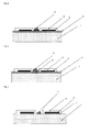
- Fig. 1 and Fig. 3 show an embodiment wherein a portion of contact between the LED device and the heat dissipating component has not been subjected to an electrical insulation treatment.
- the structure is such that a metal circuit 3 is formed on one main surface or both main surfaces of a substrate 1 consisting of a plate-shaped aluminum-graphite composite with an insulation layer 4 or active metal bonding layer 7 interposed therebetween, and an LED device (LED chip 2) positioned on the surface of the metal circuit 3 or the substrate 1 by direct brazing or the like.
- the insulation layer 4 formed on one main surface or both main surfaces of the substrate 1 is a curable resin composition having a heat-resistant resin and an inorganic filler as main components, preferably having a thermal conductivity of at least 1 W/mK after curing.
- heat-resistant resins include epoxy resins, silicone resins, polyamide resins and acrylic resins.
- the proportion of the heat-resistant used should be 10% to 40% by capacity. At less than 10% by capacity, the viscosity of the insulation layer composition rises and the workability is reduced, whereas at more than 40% by capacity, the thermal conductivity of the insulation layer 4 is reduced.
- the storage modulus of the resin composition after curing should preferably be 15000 MPa or less at 300 K.
- the curable resin composition may be formed by combining (1) a resin mainly consisting of an epoxy resin, (2) a curing agent having a polyether skeletal structure and having a primary amino group at the terminus of the main chain, and (3) an inorganic filler, thereby resulting in a cured object excelling in stress relaxation, electrical insulation, heat dissipation, heat resistance and moisture resistance.
- the epoxy resin may be any generally used epoxy resin such as a bisphenol F type epoxy resin or a bisphenol A type epoxy resin
- the balance of stress relaxation and moisture resistance can be further improved by including at least one type chosen from among epoxy resins having a dicyclopentadiene skeletal structure, epoxy resins having a naphthalene skeletal structure, epoxy resins having a biphenyl skeletal structure and epoxy resins having a novolac skeletal structure in an amount of at least 10 mass% of all epoxy resins.
- epoxy resins representative of those having a novolac skeletal structure include phenol novolac type epoxy resins and cresol novolac type epoxy resins, epoxy resins having both a novolac skeletal structure and a dicyclopentadiene skeletal structure, a naphthalene skeletal structure or a biphenyl skeletal structure may also be used.
- the epoxy resin may be an epoxy resin having an above-mentioned skeletal structure used alone.
- heat-curable resins such as phenol resins and polyimides
- macromolecular resins such as phenoxy resin, acrylic rubber and acrylonitrile-butadiene rubber
- the amount of the macromolecular resin to be added should preferably be no more than 30 mass% with respect to the total amount together with the epoxy resin.
- the curing agent which has a polyether skeletal structure and has a primary amino group on the terminus of the main chain, is used to lower the storage modulus of the resin composition after curing. It can be used in conjunction with other curing agents. When used together with an aromatic amine curing agent, the balance of stress relaxation, electrical insulation and moisture resistance can be further improved.
- aromatic amine current agents include diaminodiphenylmethane, diaminodiphenylsulfone and metaphenylenediamine. It can also be used together with a curing agent such as phenol novolac resin.
- inorganic fillers examples include oxide ceramics such as aluminum oxide (alumina), silicon oxide and magnesium oxide, nitride ceramics such as aluminum nitride, silicon nitride and boron nitride, an carbide ceramics.
- the proportion of inorganic filler in the curable resin composition should be 18% to 27% inorganic filler by volume. Outside this range, the viscosity of the resin composition will rise and the thermal conductivity will be reduced.
- the inorganic filler should consist of spherical grains having a maximum grain size of 100 ⁇ m or less and a minimum grain size of at least 0.05 ⁇ m. Furthermore, it should include 50 to 75 mass% of grains with a grain size of 5 to 50 ⁇ m, and 25 to 50 mass% of grains with a grain size of 0.2 to 1.5 ⁇ m.
- the curable resin composition constituting the insulation layer 4 may also use a silane coupler, a titanate coupler, a stabilizer or a curing promoter as needed.
- the material of the metal circuit 3 may be copper foil, aluminum foil, copper-aluminum clad foil, or copper-nickel aluminum clad foil.
- Examples of techniques for forming a metal circuit 3 on a substrate 1 composed of an aluminum-graphite composite having an insulation layer 4 interposed therebetween include the following.
- a resist ink pre-apply a resist ink to predetermined locations on the metal foil, heat or UV-cure, then etch with an etchant such as a mixture of cupric chloride, hydrogen peroxide water and sulfuric acid.
- an etchant such as a mixture of cupric chloride, hydrogen peroxide water and sulfuric acid.
- Fig. 2 shows an embodiment wherein the portion of contact between the LED device and the heat dissipating component has been subjected to an electrical insulation treatment.
- Fig. 2 shows the structure wherein a metal circuit 3 is formed on one main surface or both main surfaces of the substrate 1 consisting of an aluminum-graphite composite with the insulation layer 4 interposed therebetween, and the layers are connected via an interlayer connection bump 6 below the LED device (LED chip 2).
- a heat dissipation structure characterized by forming a metal circuit on one main surface and/or both main surfaces of the substrate 1 consisting of an aluminum-graphite composite with the active metal bonding layer 7 interposed therebetween is favorable.
- the material of the metal circuit 3 and the material of the insulation layer 4 may be the same as in the case shown in Fig. 1 .
- the method of forming an interlayer connection bump on the substrate 1 consisting of an aluminum-graphite composite may be any capable of conductively connecting the metal circuit 3 and the interlayer connection bump 6, examples of which include methods of formation by metal plating, and methods of formation by conductive paste.
- the method of forming such an insulation layer 4 having an interlayer connection bump 6 may be a method of filling the periphery and top portion of the interlayer connection bump 6 with the composition to form the insulation layer in slurry form, heating to a semi-cured state, then bonding metal foil thereto and further heating to an almost completely cured state, removing the metal circuit above the interlayer connection bump 6 by etching or the like, and removing the insulation layer composition by laser processing or the like, or a method of pre-cutting the insulation layer composition into a sheets in a semi-cured state, integrating with a metal foil by means of a hot press to form a stacking block having a raised portion at a position corresponding to the interlayer connection bump 6 and a metal layer on the surface, and removing the raised portion of the stacking block to expose an interlayer connection bump 6.
- the material of the metal circuit 3 may be Al alone, or a single Al alloy such as Al-Si alloy Al-Si-Mg alloy or Al-Mg-Mn.
- Al-Si or Al-Ge alloy or Al-Cu-Mg alloy may be used, but an Al-Cu-Mg alloy is especially preferred.
- Al-Cu-Mg alloys have a wider tolerance for bonding conditions with ceramic materials than do Al-Si type, Al-Ge type, Al-Si-Ge type or types having Mg further added to the above, so they can be bonded even if not in a vacuum, enabling bonding with exceptional productivity.
- the melting points of the Al-Si and Al-Ge types cannot be lowered without adding relatively large quantities of Si and Ge, but if too much is added, they will become hard and brittle. If, for example, the proportion of Si in an Al-Si alloy is lowered to 5% in order to avoid such problems, the melting point will be 615 °C, making bonding difficult at temperatures below 620 °C even with pressure applied.
- Al-Cu-Mg alloys are capable of bonding at temperatures of about 600 °C by taking appropriate measures such as application of pressure, even if the proportion of Cu is lowered to about 4%, thus widening the tolerance for bonding conditions.
- the Cu and Mg tends to evenly disperse in the Al as compared with Si or Ge, so localized melting is less likely to occur and excess bonding material will not tend to be squeezed out, enabling stable bonding in a relatively short time.
- the Al-Cu-Mg alloy used may be an alloy of the three components Al, Cu and Mg, and may also contain other components. For example, aside from Al, Cu and Mg, it may contain components such as Zn, In, Mn, Cr, Ti, Bi, B and Fe in a total amount of 5 wt% or less.
- the proportion of Cu in the Al-Cu-Mg alloy is preferably 2 to 6 wt%. At less than 2 wt%, the bonding temperature becomes high and too close to the melting point of Al, and at more than 6 wt%, the spread portion of the bonding material after bonding can become particularly hard, reducing the reliability of the circuit board.
- the proportion is preferably 1.5 to 5 wt%.
- Mg the bonding state can be made good by adding a small amount. This is believed to be due to the effects of removal of the oxide layer on the Al surface and effects of improving the wettability between the bonding material and the aluminum nitride substrate surface.
- the proportion of Mg is preferably 0.1 to 2 wt%.
- Examples of commercially available bonding materials that could be used include alloy 2018 containing about 4 wt% of Cu and about 0.5 wt% of Mg in Al, alloy 2017 containing about 0.5 wt% of Mn, and alloys 2001, 2005, 2007, 2014, 2024, 2030, 2034, 2036, 2048, 2090, 2117, 2124, 2214, 2218, 2224, 2324 and 7050.
- the bonding temperature a very wide range of 560 to 630 °C can be used, but the appropriate range will differ depending on the composition of the bonding material. If it contains low melting point components such as Zn or In, or a relatively high Cu or Mg content, then bonding is possible even at 600 °C or less. If the bonding temperature exceeds 630 °C, brazing and soldering defects (a "worm-eaten” effect in the circuits) can occur during bonding.
- the plate surface of the substrate 1 consisting of an aluminum-graphite composite is preferably pressed from a perpendicular direction at 10 to 100 kgf/cm 2 , particularly 15 to 80 kgf/cm 2 .
- the method of applying pressure may be placement of weights, or by mechanical application using jigs.
- the pressure should be kept within the above range at least until reaching the temperature at which bonding begins, for example, when bonding with a 95.7% Al - 4% Cu - 0.3% Mg alloy foil at a temperature of 610 °C, at least up to 580 °C.
- a metal circuit 3 for example, an Al circuit
- the substrate 1 consisting of a plate-shaped aluminum-graphite composite. While the Al-Cu-Mg alloy bonding material may be interposed between the metal plate for forming the Al circuit, the Al circuit pattern constituting the metal circuit 3 and the substrate 1, it is convenient to clad them together before hand.
- the productivity of the heat dissipating component can be greatly improved.
- bonding is not limited to vacuum furnaces. Vacuum furnaces are inherently expensive, difficult to make continuous, and have poor volume efficiency as batch furnaces. When made large, temperature distributions tend to occur, so production is not possible at high yields.
- an Al-Cu-Mg alloy is used instead of a conventional Al-Si or Al-Ge alloy bonding material, bonding is possible even if not in a vacuum, such as in a low-oxygen atmosphere of N 2 , H 2 , inert gas or a mixture thereof, enabling simple furnace structures and continuous structures. By making them continuous, the factors contributing to disparities in the product such as temperature distributions can be reduced, enabling production of products of stable quality with good yield.
- the metal plate for forming the Al circuit When producing the heat dissipating component using a metal plate for forming an Al circuit as the element for forming the metal circuit 3, it is preferable to stack the metal plate for forming the Al circuit and a substrate 1 consisting of a plate-shaped aluminum-graphite composite so that they lie adjacent, and heat them.
- the metal plate for forming the Al circuit has a higher coefficient of thermal expansion than an aluminum-graphite composite, so deformations wherein cooling after bonding results in the substrate 1 side consisting of the plate-shaped aluminum-graphite composite becoming convex are reduced.
- Al is a material that is susceptible to plastic deformation, and spacers can be interposed as needed in order to avoid adhesion between the Al materials.
- Example 1 an isotropic graphite material (Tokai Carbon G347) of bulk density 1.83 g/cm 3 , and as Example 2, an isotropic graphite material (Tokai Carbon G458) of bulk density 1.89 g/cm 3 , were worked to the shape of a rectangular parallelepiped of dimensions 200 mm ⁇ 200 mm ⁇ 250 mm, then sandwiched between iron plates of thickness 12 mm coated with a graphite mold release agent, and coupled with M10 nuts and bolts to form a stack.
- the resulting stack was preheated for 1 hour in an electric furnace with a nitrogen atmosphere at a temperature of 650 °C, then placed in a preheated press mold of inner diameter 400 mm ⁇ height 300 mm, an aluminum alloy melt containing 12 mass% of silicon was poured in, and a pressure of 100 MPa was applied for 20 minutes to infiltrate the isotropic graphite material with the aluminum alloy.
- the aluminum alloy and iron plate portions were cut with a wet band-type saw, resulting in a 200 mm ⁇ 200 mm ⁇ 250 mm aluminum-graphite composite.
- the resulting composite was annealed for 2 hours at a temperature of 500 °C to remove the residual stress from infiltration.
- the respective isotropic graphite materials were ground to form a sample (3 ⁇ 3 ⁇ 20 mm) for use in measuring the coefficient of thermal expansion in three directions and a sample (25 mm ⁇ 25 mm ⁇ 1 mm) for use in measuring the thermal conductivity.
- the respective samples were used to measure the coefficient of thermal expansion at a temperature of 25 °C to 150 °C using a thermal expansion meter (Seiko TMA 300) and to measure the thermal conductivity at 25 °C by laser flash analysis (Rigaku LF/TCM-8510B).
- the results are shown in Table 1.
- the porosity of the isotropic graphite material was calculated from the bulk density measured by Archimedes' Law using graphite of ideal density 2.2 g/cm 3 .
- the resulting aluminum-graphite composites were ground to form a sample (3 ⁇ 3 ⁇ 20 mm) for use in measuring the coefficient of thermal expansion in three directions, a sample (25 mm ⁇ 25 mm ⁇ 1 mm) for use in measuring the thermal conductivity and a sample (3 mm ⁇ 4 mm ⁇ 40 mm) for testing strength.
- the respective samples were used to measure the coefficient of thermal expansion at a temperature of 25 °C to 150 °C using a thermal expansion meter (Seiko TMA 300), the thermal conductivity at 25 °C by laser flash analysis (Rigaku LF/FCM-8510B) and the three-point bending strength (in compliance with JIS-R1601).
- the bulk density of the samples was measured by Archimedes' Law to calculate the rate of infiltration of the voids in the isotropic graphite material.
- the resulting 200 mm ⁇ 200 mm ⁇ 250 mm aluminum-graphite composites were anchored and cut under the conditions indicated in Table 3 using a multi-wire saw (Takatori MWS-612SD) having electrodeposition type wires of width 0.20 mm arranged at intervals of 1.5 mm so as to form cross sections parallel to the 200 mm ⁇ 200 mm faces of the aluminum-graphite composites.
- the cutting reserve (cut width) was 0.3 mm in all cases.
- the thicknesses of the resulting plate-shaped aluminum-graphite composites were measured using calipers, and the surface roughnesses (Ra) of the cut faces were measured using a surface roughness meter. The results are shown in Table 3.
- the plate-shaped aluminum-graphite composite obtained in Example 1 a bonding material consisting of an alloy composed of 95% Al-4% Cu-1% Mg and having a thickness of 0.3 mm, and a 0.4 mm thick Al circuit were stacked in that order to form a single set, and ten sets were stacked with spacers placed in between. These were heated for ten minutes at 610 °C in a vacuum (batch furnace) of 4 ⁇ 10 -3 Pa while applying pressure at 500 MPa in the direction perpendicular to the substrate surface consisting of an aluminum-graphite composite from outside the furnace using a hydraulic uniaxial press device via a carbon push rod, thereby bonding them together, to form an aluminum-graphite composite circuit board.
- a white solder resist (PSR4000-LEW1, Taiyo Ink) was applied via a screen onto a specific circuit, then UV-cured. Furthermore, an insulated LED chip (1 mm 2 ) was adhered over the electrolytic copper foil exposed portion by an Ag paste, resulting in an LED light emitting element as shown in Fig. 1 .
- the resulting 200 mm ⁇ 200 mm ⁇ 250 mm aluminum-graphite composite of Example 1 was anchored and cut under the conditions indicated in Table 4 using a multi-wire saw (Takatori MWS-612SD) so as to form cross sections parallel to the 200 mm ⁇ 200 mm faces of the aluminum-graphite composites.
- the thicknesses and surface roughnesses (Ra) of the resulting plate-shaped aluminum-graphite composites are shown in Table 5.
- Example 7 The isotropic graphite materials (Examples 20-26) and the extruded graphite material (Comparative Example 4) shown in Table 6 were worked into the shape of a 200 mm ⁇ 250 mm ⁇ 150 mm rectangular parallelepiped to produce an aluminum-graphite composite in the same manner as Example 1. The resulting aluminum-graphite composites were subjected to property evaluations in the same manner as Example 1. The results are shown in Table 7.
- the isotropic graphite materials of 200 mm ⁇ 200 mm ⁇ 250 mm used in Example 1 were sandwiched between iron plates of thickness 12 mm coated with a graphite mold release agent, and coupled with M10 nuts and bolts to form a stack.
- the resulting stack was subjected to the same treatment as Example 1 aside from the conditions shown in Table 8, to infiltrate the isotropic graphite materials with an aluminum alloy resulting in aluminum-graphite composites.
- the resulting composites were annealed for 2 hours at a temperature of 500 °C to remove the residual stress from infiltration, then evaluated in the same manner as Example 1. The results are shown in Table 9.
- Example 2 The material of Example 2 was cut into a plate-shaped aluminum-graphite composite of thickness 6 mm using a multi-wire saw in the same manner as Example 2 aside from the fact that the wire spacing was 6.3 mm.
- the resulting aluminum-graphite composite was worked to shape one face into fins of width 2 mm and height 5 mm spaced at intervals of 5 mm using a hard metal end mill in a machining center.
- Example 2 Using the same technique as Example 1, a non-insulated LED chip was bonded to the face on which the fins were not formed to obtain an LED light emitting element of the structure shown in Fig. 1 . Additionally, an insulated LED chip (1 mm 2 ) was bonded by an Ag paste to obtain an LED light emitting element of the structure shown in Fig. 3 .
- Example 1 The plate-shaped aluminum-graphite composite (200 mm ⁇ 200 mm ⁇ 1.2 mm) of Example 1 was ultrasonically cleaned using water, then electroless Ni-P plated to a thickness of 3 ⁇ m.
- the electroless Ni-P plating was followed by a electroless Ni-B plating to a thickness of 1 ⁇ m
- Example 36 the electroless Ni-P plating was followed by a electroless Au plating to a thickness of 1 ⁇ m, to form plating layers on the surfaces of the aluminum-graphite composites.
- the resulting plated products were of good quality, with no pin holes apparent to the naked eye. Additionally, after coating the plating surfaces with flux, they were immersed in a lead/tin eutectic solder. Over 99% of the plating surface was wetted with solder.
- Example 3 Using the same technique as Example 3, an insulated LED chip (1 mm 2 ) was bonded by Ag paste to obtain an LED light emitting element of the structure shown in Fig. 2 .
Landscapes
- Chemical & Material Sciences (AREA)
- Engineering & Computer Science (AREA)
- Ceramic Engineering (AREA)
- Materials Engineering (AREA)
- Structural Engineering (AREA)
- Organic Chemistry (AREA)
- Mechanical Engineering (AREA)
- Inorganic Chemistry (AREA)
- Manufacturing & Machinery (AREA)
- Microelectronics & Electronic Packaging (AREA)
- Cooling Or The Like Of Semiconductors Or Solid State Devices (AREA)
- Led Device Packages (AREA)
- Carbon And Carbon Compounds (AREA)
- Physics & Mathematics (AREA)
- Plasma & Fusion (AREA)
Applications Claiming Priority (2)
| Application Number | Priority Date | Filing Date | Title |
|---|---|---|---|
| JP2009029866 | 2009-02-12 | ||
| PCT/JP2010/051777 WO2010092923A1 (fr) | 2009-02-12 | 2010-02-08 | Substrat comprenant un composite d'aluminium/graphite, élément de dissipation de chaleur le comprenant et élément luminescent de del |
Publications (3)
| Publication Number | Publication Date |
|---|---|
| EP2397455A1 true EP2397455A1 (fr) | 2011-12-21 |
| EP2397455A4 EP2397455A4 (fr) | 2016-01-06 |
| EP2397455B1 EP2397455B1 (fr) | 2018-10-31 |
Family
ID=42561765
Family Applications (1)
| Application Number | Title | Priority Date | Filing Date |
|---|---|---|---|
| EP10741200.9A Active EP2397455B1 (fr) | 2009-02-12 | 2010-02-08 | Substrat comprenant un composite d'aluminium/graphite, élément de dissipation de chaleur le comprenant et élément luminescent de del |
Country Status (7)
| Country | Link |
|---|---|
| US (1) | US8883564B2 (fr) |
| EP (1) | EP2397455B1 (fr) |
| JP (1) | JP5679557B2 (fr) |
| KR (1) | KR101696945B1 (fr) |
| CN (1) | CN102317236B (fr) |
| TW (1) | TWI464114B (fr) |
| WO (1) | WO2010092923A1 (fr) |
Cited By (3)
| Publication number | Priority date | Publication date | Assignee | Title |
|---|---|---|---|---|
| EP2461379A4 (fr) * | 2009-07-31 | 2012-12-26 | Denki Kagaku Kogyo Kk | Galette pour équipements à diodes électroluminescentes, procédé de fabrication et structure équipée de diodes électroluminescentes utilisant la galette pour équipements à diodes électroluminescentes |
| EP2733181A4 (fr) * | 2011-07-13 | 2015-08-05 | Posco | Composition de résine pour un traitement de surface et tôle d'acier revêtue de celle-ci |
| TWI799909B (zh) * | 2021-07-02 | 2023-04-21 | 國碩科技工業股份有限公司 | 鑽石線切割出的散熱裝置及其製造方法 |
Families Citing this family (25)
| Publication number | Priority date | Publication date | Assignee | Title |
|---|---|---|---|---|
| JP5421751B2 (ja) * | 2009-12-03 | 2014-02-19 | スタンレー電気株式会社 | 半導体発光装置 |
| JP2012069816A (ja) * | 2010-09-24 | 2012-04-05 | Ain:Kk | アルミニウム複合材を使用した配線板 |
| CN102306694A (zh) * | 2011-05-24 | 2012-01-04 | 常州碳元科技发展有限公司 | 用于led封装的嵌套散热支架、led灯及制造方法 |
| DE102011103746A1 (de) * | 2011-05-31 | 2012-12-06 | Ixys Semiconductor Gmbh | Verfahren zum Fügen von Metall-Keramik-Substraten an Metallkörpern |
| JP5915026B2 (ja) * | 2011-08-26 | 2016-05-11 | 住友大阪セメント株式会社 | 温度測定用板状体及びそれを備えた温度測定装置 |
| CN102401361B (zh) * | 2011-11-15 | 2013-11-20 | 安徽世林照明股份有限公司 | 增加led灯铝质散热体热辐射能力的方法 |
| TW201349577A (zh) * | 2012-05-22 | 2013-12-01 | 綠晶能源股份有限公司 | 照明裝置 |
| JPWO2014057909A1 (ja) * | 2012-10-09 | 2016-09-05 | イビデン株式会社 | 蓄電デバイス用炭素材料、その製造方法及びそれを用いた蓄電デバイス |
| CN103075719A (zh) * | 2013-02-04 | 2013-05-01 | 山西山地新源科技有限公司 | 一种包覆石墨的铝散热器及其制作工艺 |
| CN104183683A (zh) * | 2013-05-24 | 2014-12-03 | 上海航天测控通信研究所 | 一种基于铝基复合材料基板的多芯片led封装方法 |
| KR101648437B1 (ko) * | 2014-06-02 | 2016-08-17 | 주식회사 티앤머티리얼스 | 탄소계 금속기지 복합체를 이용한 핀 타입 방열 기판 제조방법 |
| CN107408544B (zh) | 2015-02-03 | 2019-09-13 | 塞林克公司 | 用于组合式热能与电能传递的系统及方法 |
| TWI579492B (zh) * | 2015-05-11 | 2017-04-21 | 綠點高新科技股份有限公司 | 燈具的製造方法及該燈具 |
| JP6736389B2 (ja) * | 2015-07-10 | 2020-08-05 | 住友化学株式会社 | 焼結体の製造方法 |
| DE112016003739T5 (de) * | 2015-08-17 | 2018-04-26 | Nlight, Inc. | Wärmespreizer mit optimiertem Wärmeausdehnungskoeffizienten und/oder Wärmeübergang |
| CN105922675B (zh) * | 2016-04-25 | 2018-06-12 | 东莞市联洲知识产权运营管理有限公司 | 一种铝基金刚石igbt散热基板材料及其制备方法 |
| CN106972096A (zh) * | 2016-10-26 | 2017-07-21 | 湾城公司 | 一种散热构造体及应用 |
| CN107737891B (zh) * | 2017-09-26 | 2019-08-23 | 湖北中一科技股份有限公司 | 一种结晶器的石墨套的制作方法 |
| CN111971789B (zh) | 2018-03-28 | 2024-03-01 | 株式会社钟化 | 各向异性石墨、各向异性石墨复合体及其制造方法 |
| JP7049951B2 (ja) * | 2018-07-11 | 2022-04-07 | 昭和電工株式会社 | 積層材 |
| US10903618B2 (en) * | 2019-03-20 | 2021-01-26 | Chroma Ate Inc. | Fixture assembly for testing edge-emitting laser diodes and testing apparatus having the same |
| US11289399B2 (en) * | 2019-09-26 | 2022-03-29 | Taiwan Semiconductor Manufacturing Company, Ltd. | Package structure and manufacturing method thereof |
| RU2753635C1 (ru) * | 2020-12-21 | 2021-08-18 | Федеральное государственное бюджетное образовательное учреждение высшего образования «Волгоградский государственный технический университет» (ВолгГТУ) | Способ получения углеграфитового композиционного материала |
| RU2751859C1 (ru) * | 2020-12-22 | 2021-07-19 | Федеральное государственное бюджетное образовательное учреждение высшего образования "Волгоградский государственный технический университет" (ВолгГТУ) | Способ получения углеграфитового композиционного материала |
| CN118636311B (zh) * | 2024-07-11 | 2024-11-05 | 三剑(苏州)新材料科技有限公司 | 一种石墨柱体内取盲孔的加工工艺及其装置 |
Family Cites Families (18)
| Publication number | Priority date | Publication date | Assignee | Title |
|---|---|---|---|---|
| JP3082152B2 (ja) | 1992-06-05 | 2000-08-28 | 東海カーボン株式会社 | ピストン用素材とその製造方法 |
| EP1055650B1 (fr) | 1998-11-11 | 2014-10-29 | Totankako Co., Ltd. | Materiau composite metallique a base de carbone, et procedes de preparation et d'utilisation correspondants |
| JP3673436B2 (ja) | 1998-11-11 | 2005-07-20 | 東炭化工株式会社 | 炭素基金属複合材料およびその製造方法 |
| JP3468358B2 (ja) | 1998-11-12 | 2003-11-17 | 電気化学工業株式会社 | 炭化珪素質複合体及びその製造方法とそれを用いた放熱部品 |
| JP2000158318A (ja) | 1998-11-27 | 2000-06-13 | Fujikoshi Mach Corp | ダイヤモンドワイヤーソー |
| JP3351778B2 (ja) * | 1999-06-11 | 2002-12-03 | 日本政策投資銀行 | 炭素基金属複合材料板状成形体および製造方法 |
| JP2001339022A (ja) * | 1999-12-24 | 2001-12-07 | Ngk Insulators Ltd | ヒートシンク材及びその製造方法 |
| US6933531B1 (en) | 1999-12-24 | 2005-08-23 | Ngk Insulators, Ltd. | Heat sink material and method of manufacturing the heat sink material |
| JP2003201528A (ja) * | 2001-10-26 | 2003-07-18 | Ngk Insulators Ltd | ヒートシンク材 |
| JP4344934B2 (ja) * | 2003-05-16 | 2009-10-14 | 日立金属株式会社 | 高熱伝導・低熱膨張複合材及び放熱基板並びにこれらの製造方法 |
| EP1477467B1 (fr) | 2003-05-16 | 2012-05-23 | Hitachi Metals, Ltd. | Matériau composite à haute conductivité thermique et faible coefficient d'expansion thermique, et puits thermique. |
| TWI234295B (en) | 2003-10-08 | 2005-06-11 | Epistar Corp | High-efficiency nitride-based light-emitting device |
| WO2005037968A1 (fr) * | 2003-10-16 | 2005-04-28 | Mitsubishi Denki Kabushiki Kaisha | Boue pour decouper des lingots de silicium et procede de decoupage de lingots de silicium au moyen de ladite boue |
| JP4711165B2 (ja) * | 2004-06-21 | 2011-06-29 | 日立金属株式会社 | 高熱伝導・低熱膨脹複合体およびその製造方法 |
| EP1858078A4 (fr) * | 2005-01-20 | 2009-03-04 | Almt Corp | Element pour un dispositif semi-conducteur et procede pour sa fabrication |
| US20080128067A1 (en) * | 2006-10-08 | 2008-06-05 | Momentive Performance Materials Inc. | Heat transfer composite, associated device and method |
| JP2008305917A (ja) * | 2007-06-06 | 2008-12-18 | Bando Chem Ind Ltd | 放熱シートの製造方法 |
| US20090080189A1 (en) * | 2007-09-21 | 2009-03-26 | Cooper Technologies Company | Optic Coupler for Light Emitting Diode Fixture |
-
2010
- 2010-02-08 CN CN201080007857.6A patent/CN102317236B/zh active Active
- 2010-02-08 JP JP2010550506A patent/JP5679557B2/ja active Active
- 2010-02-08 WO PCT/JP2010/051777 patent/WO2010092923A1/fr not_active Ceased
- 2010-02-08 US US13/148,977 patent/US8883564B2/en active Active
- 2010-02-08 EP EP10741200.9A patent/EP2397455B1/fr active Active
- 2010-02-08 KR KR1020117020362A patent/KR101696945B1/ko active Active
- 2010-02-11 TW TW99104277A patent/TWI464114B/zh active
Non-Patent Citations (1)
| Title |
|---|
| See references of WO2010092923A1 * |
Cited By (5)
| Publication number | Priority date | Publication date | Assignee | Title |
|---|---|---|---|---|
| EP2461379A4 (fr) * | 2009-07-31 | 2012-12-26 | Denki Kagaku Kogyo Kk | Galette pour équipements à diodes électroluminescentes, procédé de fabrication et structure équipée de diodes électroluminescentes utilisant la galette pour équipements à diodes électroluminescentes |
| US8890189B2 (en) | 2009-07-31 | 2014-11-18 | Denki Kagaku Kogyo Kabushiki Kaisha | Wafer for LED mounting, method for manufacturing same, and LED-mounted structure using the wafer |
| EP2733181A4 (fr) * | 2011-07-13 | 2015-08-05 | Posco | Composition de résine pour un traitement de surface et tôle d'acier revêtue de celle-ci |
| US9376576B2 (en) | 2011-07-13 | 2016-06-28 | Posco | Resin composition for a surface treatment, and steel sheet coated with same |
| TWI799909B (zh) * | 2021-07-02 | 2023-04-21 | 國碩科技工業股份有限公司 | 鑽石線切割出的散熱裝置及其製造方法 |
Also Published As
| Publication number | Publication date |
|---|---|
| US20110316038A1 (en) | 2011-12-29 |
| JPWO2010092923A1 (ja) | 2012-08-16 |
| EP2397455B1 (fr) | 2018-10-31 |
| KR20110117694A (ko) | 2011-10-27 |
| WO2010092923A1 (fr) | 2010-08-19 |
| TW201105577A (en) | 2011-02-16 |
| CN102317236B (zh) | 2014-04-09 |
| TWI464114B (zh) | 2014-12-11 |
| JP5679557B2 (ja) | 2015-03-04 |
| US8883564B2 (en) | 2014-11-11 |
| KR101696945B1 (ko) | 2017-01-16 |
| EP2397455A4 (fr) | 2016-01-06 |
| CN102317236A (zh) | 2012-01-11 |
Similar Documents
| Publication | Publication Date | Title |
|---|---|---|
| EP2397455B1 (fr) | Substrat comprenant un composite d'aluminium/graphite, élément de dissipation de chaleur le comprenant et élément luminescent de del | |
| US8546842B2 (en) | LED chip assembly, LED package, and manufacturing method of LED package | |
| JP6462899B2 (ja) | 高出力素子用放熱板材 | |
| KR101419627B1 (ko) | 파워 모듈용 기판 및 파워 모듈 | |
| JP5061018B2 (ja) | アルミニウム−黒鉛−炭化珪素質複合体及びその製造方法 | |
| KR20110033117A (ko) | 파워 모듈용 기판, 파워 모듈, 및 파워 모듈용 기판의 제조 방법 | |
| CN112839799A (zh) | 带金属层的碳质构件及导热板 | |
| JP5699442B2 (ja) | パワーモジュール用基板及びパワーモジュール | |
| JP5361273B2 (ja) | アルミニウム−黒鉛質複合体、それを用いた回路基板及びその製造方法 | |
| JP5676278B2 (ja) | アルミニウム−黒鉛複合体、それを用いた放熱部品及びled発光部材 | |
| JP5646473B2 (ja) | アルミニウム−黒鉛質複合体、それを用いた放熱部品及びled発光部材 | |
| JP5681035B2 (ja) | Led光源パッケージ | |
| JP5659542B2 (ja) | 絶縁基板及びパワーモジュール | |
| JP5759376B2 (ja) | Ledチップ接合体の製造方法 | |
| CN120261416A (zh) | 一种复合结构及其制备方法、封装结构及电子器件 |
Legal Events
| Date | Code | Title | Description |
|---|---|---|---|
| PUAI | Public reference made under article 153(3) epc to a published international application that has entered the european phase |
Free format text: ORIGINAL CODE: 0009012 |
|
| 17P | Request for examination filed |
Effective date: 20110802 |
|
| AK | Designated contracting states |
Kind code of ref document: A1 Designated state(s): AT BE BG CH CY CZ DE DK EE ES FI FR GB GR HR HU IE IS IT LI LT LU LV MC MK MT NL NO PL PT RO SE SI SK SM TR |
|
| DAX | Request for extension of the european patent (deleted) | ||
| RA4 | Supplementary search report drawn up and despatched (corrected) |
Effective date: 20151203 |
|
| RIC1 | Information provided on ipc code assigned before grant |
Ipc: C04B 111/00 20060101ALN20151127BHEP Ipc: C04B 41/00 20060101ALI20151127BHEP Ipc: B23D 57/00 20060101ALI20151127BHEP Ipc: H01L 23/14 20060101ALI20151127BHEP Ipc: B23D 61/18 20060101ALI20151127BHEP Ipc: C04B 41/51 20060101ALI20151127BHEP Ipc: B28D 5/04 20060101ALI20151127BHEP Ipc: H01L 23/373 20060101ALI20151127BHEP Ipc: H01L 33/64 20100101ALN20151127BHEP Ipc: H05K 1/05 20060101ALI20151127BHEP Ipc: B22F 3/26 20060101ALI20151127BHEP Ipc: C04B 41/88 20060101AFI20151127BHEP |
|
| RAP1 | Party data changed (applicant data changed or rights of an application transferred) |
Owner name: DENKA COMPANY LIMITED |
|
| STAA | Information on the status of an ep patent application or granted ep patent |
Free format text: STATUS: EXAMINATION IS IN PROGRESS |
|
| 17Q | First examination report despatched |
Effective date: 20170509 |
|
| RIC1 | Information provided on ipc code assigned before grant |
Ipc: B22F 3/26 20060101ALI20180412BHEP Ipc: H01L 33/64 20100101ALN20180412BHEP Ipc: B23D 57/00 20060101ALI20180412BHEP Ipc: C04B 41/51 20060101ALI20180412BHEP Ipc: H01L 23/14 20060101ALI20180412BHEP Ipc: B28D 5/04 20060101ALI20180412BHEP Ipc: H01L 23/373 20060101ALI20180412BHEP Ipc: H05K 1/05 20060101ALI20180412BHEP Ipc: C04B 41/88 20060101AFI20180412BHEP Ipc: C04B 41/00 20060101ALI20180412BHEP Ipc: C04B 111/00 20060101ALN20180412BHEP Ipc: B23D 61/18 20060101ALI20180412BHEP |
|
| GRAP | Despatch of communication of intention to grant a patent |
Free format text: ORIGINAL CODE: EPIDOSNIGR1 |
|
| STAA | Information on the status of an ep patent application or granted ep patent |
Free format text: STATUS: GRANT OF PATENT IS INTENDED |
|
| INTG | Intention to grant announced |
Effective date: 20180524 |
|
| GRAS | Grant fee paid |
Free format text: ORIGINAL CODE: EPIDOSNIGR3 |
|
| GRAA | (expected) grant |
Free format text: ORIGINAL CODE: 0009210 |
|
| STAA | Information on the status of an ep patent application or granted ep patent |
Free format text: STATUS: THE PATENT HAS BEEN GRANTED |
|
| RIN1 | Information on inventor provided before grant (corrected) |
Inventor name: NARITA SHINYA Inventor name: HIROTSURU HIDEKI Inventor name: TSUJIMURA YOSHIHIKO Inventor name: HIGUMA SATOSHI |
|
| AK | Designated contracting states |
Kind code of ref document: B1 Designated state(s): AT BE BG CH CY CZ DE DK EE ES FI FR GB GR HR HU IE IS IT LI LT LU LV MC MK MT NL NO PL PT RO SE SI SK SM TR |
|
| REG | Reference to a national code |
Ref country code: CH Ref legal event code: EP Ref country code: GB Ref legal event code: FG4D |
|
| REG | Reference to a national code |
Ref country code: AT Ref legal event code: REF Ref document number: 1059185 Country of ref document: AT Kind code of ref document: T Effective date: 20181115 |
|
| REG | Reference to a national code |
Ref country code: IE Ref legal event code: FG4D |
|
| REG | Reference to a national code |
Ref country code: DE Ref legal event code: R096 Ref document number: 602010054766 Country of ref document: DE |
|
| REG | Reference to a national code |
Ref country code: NL Ref legal event code: MP Effective date: 20181031 |
|
| REG | Reference to a national code |
Ref country code: LT Ref legal event code: MG4D |
|
| REG | Reference to a national code |
Ref country code: AT Ref legal event code: MK05 Ref document number: 1059185 Country of ref document: AT Kind code of ref document: T Effective date: 20181031 |
|
| PG25 | Lapsed in a contracting state [announced via postgrant information from national office to epo] |
Ref country code: HR Free format text: LAPSE BECAUSE OF FAILURE TO SUBMIT A TRANSLATION OF THE DESCRIPTION OR TO PAY THE FEE WITHIN THE PRESCRIBED TIME-LIMIT Effective date: 20181031 Ref country code: PL Free format text: LAPSE BECAUSE OF FAILURE TO SUBMIT A TRANSLATION OF THE DESCRIPTION OR TO PAY THE FEE WITHIN THE PRESCRIBED TIME-LIMIT Effective date: 20181031 Ref country code: NO Free format text: LAPSE BECAUSE OF FAILURE TO SUBMIT A TRANSLATION OF THE DESCRIPTION OR TO PAY THE FEE WITHIN THE PRESCRIBED TIME-LIMIT Effective date: 20190131 Ref country code: AT Free format text: LAPSE BECAUSE OF FAILURE TO SUBMIT A TRANSLATION OF THE DESCRIPTION OR TO PAY THE FEE WITHIN THE PRESCRIBED TIME-LIMIT Effective date: 20181031 Ref country code: IS Free format text: LAPSE BECAUSE OF FAILURE TO SUBMIT A TRANSLATION OF THE DESCRIPTION OR TO PAY THE FEE WITHIN THE PRESCRIBED TIME-LIMIT Effective date: 20190228 Ref country code: LV Free format text: LAPSE BECAUSE OF FAILURE TO SUBMIT A TRANSLATION OF THE DESCRIPTION OR TO PAY THE FEE WITHIN THE PRESCRIBED TIME-LIMIT Effective date: 20181031 Ref country code: FI Free format text: LAPSE BECAUSE OF FAILURE TO SUBMIT A TRANSLATION OF THE DESCRIPTION OR TO PAY THE FEE WITHIN THE PRESCRIBED TIME-LIMIT Effective date: 20181031 Ref country code: ES Free format text: LAPSE BECAUSE OF FAILURE TO SUBMIT A TRANSLATION OF THE DESCRIPTION OR TO PAY THE FEE WITHIN THE PRESCRIBED TIME-LIMIT Effective date: 20181031 Ref country code: BG Free format text: LAPSE BECAUSE OF FAILURE TO SUBMIT A TRANSLATION OF THE DESCRIPTION OR TO PAY THE FEE WITHIN THE PRESCRIBED TIME-LIMIT Effective date: 20190131 Ref country code: LT Free format text: LAPSE BECAUSE OF FAILURE TO SUBMIT A TRANSLATION OF THE DESCRIPTION OR TO PAY THE FEE WITHIN THE PRESCRIBED TIME-LIMIT Effective date: 20181031 |
|
| PG25 | Lapsed in a contracting state [announced via postgrant information from national office to epo] |
Ref country code: PT Free format text: LAPSE BECAUSE OF FAILURE TO SUBMIT A TRANSLATION OF THE DESCRIPTION OR TO PAY THE FEE WITHIN THE PRESCRIBED TIME-LIMIT Effective date: 20190301 Ref country code: NL Free format text: LAPSE BECAUSE OF FAILURE TO SUBMIT A TRANSLATION OF THE DESCRIPTION OR TO PAY THE FEE WITHIN THE PRESCRIBED TIME-LIMIT Effective date: 20181031 Ref country code: GR Free format text: LAPSE BECAUSE OF FAILURE TO SUBMIT A TRANSLATION OF THE DESCRIPTION OR TO PAY THE FEE WITHIN THE PRESCRIBED TIME-LIMIT Effective date: 20190201 Ref country code: SE Free format text: LAPSE BECAUSE OF FAILURE TO SUBMIT A TRANSLATION OF THE DESCRIPTION OR TO PAY THE FEE WITHIN THE PRESCRIBED TIME-LIMIT Effective date: 20181031 |
|
| PG25 | Lapsed in a contracting state [announced via postgrant information from national office to epo] |
Ref country code: CZ Free format text: LAPSE BECAUSE OF FAILURE TO SUBMIT A TRANSLATION OF THE DESCRIPTION OR TO PAY THE FEE WITHIN THE PRESCRIBED TIME-LIMIT Effective date: 20181031 Ref country code: IT Free format text: LAPSE BECAUSE OF FAILURE TO SUBMIT A TRANSLATION OF THE DESCRIPTION OR TO PAY THE FEE WITHIN THE PRESCRIBED TIME-LIMIT Effective date: 20181031 Ref country code: DK Free format text: LAPSE BECAUSE OF FAILURE TO SUBMIT A TRANSLATION OF THE DESCRIPTION OR TO PAY THE FEE WITHIN THE PRESCRIBED TIME-LIMIT Effective date: 20181031 |
|
| REG | Reference to a national code |
Ref country code: DE Ref legal event code: R097 Ref document number: 602010054766 Country of ref document: DE |
|
| PG25 | Lapsed in a contracting state [announced via postgrant information from national office to epo] |
Ref country code: SK Free format text: LAPSE BECAUSE OF FAILURE TO SUBMIT A TRANSLATION OF THE DESCRIPTION OR TO PAY THE FEE WITHIN THE PRESCRIBED TIME-LIMIT Effective date: 20181031 Ref country code: SM Free format text: LAPSE BECAUSE OF FAILURE TO SUBMIT A TRANSLATION OF THE DESCRIPTION OR TO PAY THE FEE WITHIN THE PRESCRIBED TIME-LIMIT Effective date: 20181031 Ref country code: EE Free format text: LAPSE BECAUSE OF FAILURE TO SUBMIT A TRANSLATION OF THE DESCRIPTION OR TO PAY THE FEE WITHIN THE PRESCRIBED TIME-LIMIT Effective date: 20181031 Ref country code: RO Free format text: LAPSE BECAUSE OF FAILURE TO SUBMIT A TRANSLATION OF THE DESCRIPTION OR TO PAY THE FEE WITHIN THE PRESCRIBED TIME-LIMIT Effective date: 20181031 |
|
| PLBE | No opposition filed within time limit |
Free format text: ORIGINAL CODE: 0009261 |
|
| STAA | Information on the status of an ep patent application or granted ep patent |
Free format text: STATUS: NO OPPOSITION FILED WITHIN TIME LIMIT |
|
| REG | Reference to a national code |
Ref country code: CH Ref legal event code: PL |
|
| 26N | No opposition filed |
Effective date: 20190801 |
|
| GBPC | Gb: european patent ceased through non-payment of renewal fee |
Effective date: 20190208 |
|
| PG25 | Lapsed in a contracting state [announced via postgrant information from national office to epo] |
Ref country code: MC Free format text: LAPSE BECAUSE OF FAILURE TO SUBMIT A TRANSLATION OF THE DESCRIPTION OR TO PAY THE FEE WITHIN THE PRESCRIBED TIME-LIMIT Effective date: 20181031 Ref country code: LU Free format text: LAPSE BECAUSE OF NON-PAYMENT OF DUE FEES Effective date: 20190208 Ref country code: SI Free format text: LAPSE BECAUSE OF FAILURE TO SUBMIT A TRANSLATION OF THE DESCRIPTION OR TO PAY THE FEE WITHIN THE PRESCRIBED TIME-LIMIT Effective date: 20181031 |
|
| REG | Reference to a national code |
Ref country code: BE Ref legal event code: MM Effective date: 20190228 |
|
| REG | Reference to a national code |
Ref country code: IE Ref legal event code: MM4A |
|
| PG25 | Lapsed in a contracting state [announced via postgrant information from national office to epo] |
Ref country code: LI Free format text: LAPSE BECAUSE OF NON-PAYMENT OF DUE FEES Effective date: 20190228 Ref country code: CH Free format text: LAPSE BECAUSE OF NON-PAYMENT OF DUE FEES Effective date: 20190228 |
|
| PG25 | Lapsed in a contracting state [announced via postgrant information from national office to epo] |
Ref country code: GB Free format text: LAPSE BECAUSE OF NON-PAYMENT OF DUE FEES Effective date: 20190208 Ref country code: IE Free format text: LAPSE BECAUSE OF NON-PAYMENT OF DUE FEES Effective date: 20190208 |
|
| PG25 | Lapsed in a contracting state [announced via postgrant information from national office to epo] |
Ref country code: FR Free format text: LAPSE BECAUSE OF NON-PAYMENT OF DUE FEES Effective date: 20190228 Ref country code: BE Free format text: LAPSE BECAUSE OF NON-PAYMENT OF DUE FEES Effective date: 20190228 |
|
| PG25 | Lapsed in a contracting state [announced via postgrant information from national office to epo] |
Ref country code: TR Free format text: LAPSE BECAUSE OF FAILURE TO SUBMIT A TRANSLATION OF THE DESCRIPTION OR TO PAY THE FEE WITHIN THE PRESCRIBED TIME-LIMIT Effective date: 20181031 |
|
| PG25 | Lapsed in a contracting state [announced via postgrant information from national office to epo] |
Ref country code: MT Free format text: LAPSE BECAUSE OF NON-PAYMENT OF DUE FEES Effective date: 20190208 |
|
| PG25 | Lapsed in a contracting state [announced via postgrant information from national office to epo] |
Ref country code: CY Free format text: LAPSE BECAUSE OF FAILURE TO SUBMIT A TRANSLATION OF THE DESCRIPTION OR TO PAY THE FEE WITHIN THE PRESCRIBED TIME-LIMIT Effective date: 20181031 |
|
| PG25 | Lapsed in a contracting state [announced via postgrant information from national office to epo] |
Ref country code: HU Free format text: LAPSE BECAUSE OF FAILURE TO SUBMIT A TRANSLATION OF THE DESCRIPTION OR TO PAY THE FEE WITHIN THE PRESCRIBED TIME-LIMIT; INVALID AB INITIO Effective date: 20100208 |
|
| PG25 | Lapsed in a contracting state [announced via postgrant information from national office to epo] |
Ref country code: MK Free format text: LAPSE BECAUSE OF FAILURE TO SUBMIT A TRANSLATION OF THE DESCRIPTION OR TO PAY THE FEE WITHIN THE PRESCRIBED TIME-LIMIT Effective date: 20181031 |
|
| P01 | Opt-out of the competence of the unified patent court (upc) registered |
Effective date: 20230512 |
|
| PGFP | Annual fee paid to national office [announced via postgrant information from national office to epo] |
Ref country code: DE Payment date: 20241231 Year of fee payment: 16 |