EP2409832B1 - Radiowellen übertragender schmuckfilm und schmuckelement damit - Google Patents
Radiowellen übertragender schmuckfilm und schmuckelement damit Download PDFInfo
- Publication number
- EP2409832B1 EP2409832B1 EP10753275.6A EP10753275A EP2409832B1 EP 2409832 B1 EP2409832 B1 EP 2409832B1 EP 10753275 A EP10753275 A EP 10753275A EP 2409832 B1 EP2409832 B1 EP 2409832B1
- Authority
- EP
- European Patent Office
- Prior art keywords
- light
- film
- reflecting layer
- polymer film
- decorative
- Prior art date
- Legal status (The legal status is an assumption and is not a legal conclusion. Google has not performed a legal analysis and makes no representation as to the accuracy of the status listed.)
- Not-in-force
Links
Images



Classifications
-
- C—CHEMISTRY; METALLURGY
- C23—COATING METALLIC MATERIAL; COATING MATERIAL WITH METALLIC MATERIAL; CHEMICAL SURFACE TREATMENT; DIFFUSION TREATMENT OF METALLIC MATERIAL; COATING BY VACUUM EVAPORATION, BY SPUTTERING, BY ION IMPLANTATION OR BY CHEMICAL VAPOUR DEPOSITION, IN GENERAL; INHIBITING CORROSION OF METALLIC MATERIAL OR INCRUSTATION IN GENERAL
- C23C—COATING METALLIC MATERIAL; COATING MATERIAL WITH METALLIC MATERIAL; SURFACE TREATMENT OF METALLIC MATERIAL BY DIFFUSION INTO THE SURFACE, BY CHEMICAL CONVERSION OR SUBSTITUTION; COATING BY VACUUM EVAPORATION, BY SPUTTERING, BY ION IMPLANTATION OR BY CHEMICAL VAPOUR DEPOSITION, IN GENERAL
- C23C14/00—Coating by vacuum evaporation, by sputtering or by ion implantation of the coating forming material
- C23C14/06—Coating by vacuum evaporation, by sputtering or by ion implantation of the coating forming material characterised by the coating material
- C23C14/14—Metallic material, boron or silicon
- C23C14/20—Metallic material, boron or silicon on organic substrates
-
- B—PERFORMING OPERATIONS; TRANSPORTING
- B32—LAYERED PRODUCTS
- B32B—LAYERED PRODUCTS, i.e. PRODUCTS BUILT-UP OF STRATA OF FLAT OR NON-FLAT, e.g. CELLULAR OR HONEYCOMB, FORM
- B32B27/00—Layered products comprising a layer of synthetic resin
- B32B27/06—Layered products comprising a layer of synthetic resin as the main or only constituent of a layer, which is next to another layer of the same or of a different material
- B32B27/08—Layered products comprising a layer of synthetic resin as the main or only constituent of a layer, which is next to another layer of the same or of a different material of synthetic resin
-
- B—PERFORMING OPERATIONS; TRANSPORTING
- B32—LAYERED PRODUCTS
- B32B—LAYERED PRODUCTS, i.e. PRODUCTS BUILT-UP OF STRATA OF FLAT OR NON-FLAT, e.g. CELLULAR OR HONEYCOMB, FORM
- B32B27/00—Layered products comprising a layer of synthetic resin
- B32B27/30—Layered products comprising a layer of synthetic resin comprising vinyl (co)polymers; comprising acrylic (co)polymers
- B32B27/302—Layered products comprising a layer of synthetic resin comprising vinyl (co)polymers; comprising acrylic (co)polymers comprising aromatic vinyl (co)polymers, e.g. styrenic (co)polymers
-
- B—PERFORMING OPERATIONS; TRANSPORTING
- B32—LAYERED PRODUCTS
- B32B—LAYERED PRODUCTS, i.e. PRODUCTS BUILT-UP OF STRATA OF FLAT OR NON-FLAT, e.g. CELLULAR OR HONEYCOMB, FORM
- B32B27/00—Layered products comprising a layer of synthetic resin
- B32B27/30—Layered products comprising a layer of synthetic resin comprising vinyl (co)polymers; comprising acrylic (co)polymers
- B32B27/304—Layered products comprising a layer of synthetic resin comprising vinyl (co)polymers; comprising acrylic (co)polymers comprising vinyl halide (co)polymers, e.g. PVC, PVDC, PVF, PVDF
-
- B—PERFORMING OPERATIONS; TRANSPORTING
- B32—LAYERED PRODUCTS
- B32B—LAYERED PRODUCTS, i.e. PRODUCTS BUILT-UP OF STRATA OF FLAT OR NON-FLAT, e.g. CELLULAR OR HONEYCOMB, FORM
- B32B27/00—Layered products comprising a layer of synthetic resin
- B32B27/30—Layered products comprising a layer of synthetic resin comprising vinyl (co)polymers; comprising acrylic (co)polymers
- B32B27/306—Layered products comprising a layer of synthetic resin comprising vinyl (co)polymers; comprising acrylic (co)polymers comprising vinyl acetate or vinyl alcohol (co)polymers
-
- B—PERFORMING OPERATIONS; TRANSPORTING
- B32—LAYERED PRODUCTS
- B32B—LAYERED PRODUCTS, i.e. PRODUCTS BUILT-UP OF STRATA OF FLAT OR NON-FLAT, e.g. CELLULAR OR HONEYCOMB, FORM
- B32B27/00—Layered products comprising a layer of synthetic resin
- B32B27/30—Layered products comprising a layer of synthetic resin comprising vinyl (co)polymers; comprising acrylic (co)polymers
- B32B27/308—Layered products comprising a layer of synthetic resin comprising vinyl (co)polymers; comprising acrylic (co)polymers comprising acrylic (co)polymers
-
- B—PERFORMING OPERATIONS; TRANSPORTING
- B32—LAYERED PRODUCTS
- B32B—LAYERED PRODUCTS, i.e. PRODUCTS BUILT-UP OF STRATA OF FLAT OR NON-FLAT, e.g. CELLULAR OR HONEYCOMB, FORM
- B32B27/00—Layered products comprising a layer of synthetic resin
- B32B27/32—Layered products comprising a layer of synthetic resin comprising polyolefins
-
- B—PERFORMING OPERATIONS; TRANSPORTING
- B32—LAYERED PRODUCTS
- B32B—LAYERED PRODUCTS, i.e. PRODUCTS BUILT-UP OF STRATA OF FLAT OR NON-FLAT, e.g. CELLULAR OR HONEYCOMB, FORM
- B32B27/00—Layered products comprising a layer of synthetic resin
- B32B27/32—Layered products comprising a layer of synthetic resin comprising polyolefins
- B32B27/325—Layered products comprising a layer of synthetic resin comprising polyolefins comprising polycycloolefins
-
- B—PERFORMING OPERATIONS; TRANSPORTING
- B32—LAYERED PRODUCTS
- B32B—LAYERED PRODUCTS, i.e. PRODUCTS BUILT-UP OF STRATA OF FLAT OR NON-FLAT, e.g. CELLULAR OR HONEYCOMB, FORM
- B32B27/00—Layered products comprising a layer of synthetic resin
- B32B27/36—Layered products comprising a layer of synthetic resin comprising polyesters
-
- B—PERFORMING OPERATIONS; TRANSPORTING
- B32—LAYERED PRODUCTS
- B32B—LAYERED PRODUCTS, i.e. PRODUCTS BUILT-UP OF STRATA OF FLAT OR NON-FLAT, e.g. CELLULAR OR HONEYCOMB, FORM
- B32B27/00—Layered products comprising a layer of synthetic resin
- B32B27/36—Layered products comprising a layer of synthetic resin comprising polyesters
- B32B27/365—Layered products comprising a layer of synthetic resin comprising polyesters comprising polycarbonates
-
- B—PERFORMING OPERATIONS; TRANSPORTING
- B32—LAYERED PRODUCTS
- B32B—LAYERED PRODUCTS, i.e. PRODUCTS BUILT-UP OF STRATA OF FLAT OR NON-FLAT, e.g. CELLULAR OR HONEYCOMB, FORM
- B32B27/00—Layered products comprising a layer of synthetic resin
- B32B27/40—Layered products comprising a layer of synthetic resin comprising polyurethanes
-
- B—PERFORMING OPERATIONS; TRANSPORTING
- B32—LAYERED PRODUCTS
- B32B—LAYERED PRODUCTS, i.e. PRODUCTS BUILT-UP OF STRATA OF FLAT OR NON-FLAT, e.g. CELLULAR OR HONEYCOMB, FORM
- B32B7/00—Layered products characterised by the relation between layers; Layered products characterised by the relative orientation of features between layers, or by the relative values of a measurable parameter between layers, i.e. products comprising layers having different physical, chemical or physicochemical properties; Layered products characterised by the interconnection of layers
- B32B7/04—Interconnection of layers
- B32B7/12—Interconnection of layers using interposed adhesives or interposed materials with bonding properties
-
- B—PERFORMING OPERATIONS; TRANSPORTING
- B32—LAYERED PRODUCTS
- B32B—LAYERED PRODUCTS, i.e. PRODUCTS BUILT-UP OF STRATA OF FLAT OR NON-FLAT, e.g. CELLULAR OR HONEYCOMB, FORM
- B32B2250/00—Layers arrangement
- B32B2250/24—All layers being polymeric
-
- B—PERFORMING OPERATIONS; TRANSPORTING
- B32—LAYERED PRODUCTS
- B32B—LAYERED PRODUCTS, i.e. PRODUCTS BUILT-UP OF STRATA OF FLAT OR NON-FLAT, e.g. CELLULAR OR HONEYCOMB, FORM
- B32B2255/00—Coating on the layer surface
- B32B2255/10—Coating on the layer surface on synthetic resin layer or on natural or synthetic rubber layer
-
- B—PERFORMING OPERATIONS; TRANSPORTING
- B32—LAYERED PRODUCTS
- B32B—LAYERED PRODUCTS, i.e. PRODUCTS BUILT-UP OF STRATA OF FLAT OR NON-FLAT, e.g. CELLULAR OR HONEYCOMB, FORM
- B32B2255/00—Coating on the layer surface
- B32B2255/20—Inorganic coating
- B32B2255/205—Metallic coating
-
- B—PERFORMING OPERATIONS; TRANSPORTING
- B32—LAYERED PRODUCTS
- B32B—LAYERED PRODUCTS, i.e. PRODUCTS BUILT-UP OF STRATA OF FLAT OR NON-FLAT, e.g. CELLULAR OR HONEYCOMB, FORM
- B32B2307/00—Properties of the layers or laminate
- B32B2307/20—Properties of the layers or laminate having particular electrical or magnetic properties, e.g. piezoelectric
-
- B—PERFORMING OPERATIONS; TRANSPORTING
- B32—LAYERED PRODUCTS
- B32B—LAYERED PRODUCTS, i.e. PRODUCTS BUILT-UP OF STRATA OF FLAT OR NON-FLAT, e.g. CELLULAR OR HONEYCOMB, FORM
- B32B2307/00—Properties of the layers or laminate
- B32B2307/40—Properties of the layers or laminate having particular optical properties
- B32B2307/406—Bright, glossy, shiny surface
-
- B—PERFORMING OPERATIONS; TRANSPORTING
- B32—LAYERED PRODUCTS
- B32B—LAYERED PRODUCTS, i.e. PRODUCTS BUILT-UP OF STRATA OF FLAT OR NON-FLAT, e.g. CELLULAR OR HONEYCOMB, FORM
- B32B2307/00—Properties of the layers or laminate
- B32B2307/40—Properties of the layers or laminate having particular optical properties
- B32B2307/412—Transparent
-
- B—PERFORMING OPERATIONS; TRANSPORTING
- B32—LAYERED PRODUCTS
- B32B—LAYERED PRODUCTS, i.e. PRODUCTS BUILT-UP OF STRATA OF FLAT OR NON-FLAT, e.g. CELLULAR OR HONEYCOMB, FORM
- B32B2307/00—Properties of the layers or laminate
- B32B2307/40—Properties of the layers or laminate having particular optical properties
- B32B2307/416—Reflective
-
- B—PERFORMING OPERATIONS; TRANSPORTING
- B32—LAYERED PRODUCTS
- B32B—LAYERED PRODUCTS, i.e. PRODUCTS BUILT-UP OF STRATA OF FLAT OR NON-FLAT, e.g. CELLULAR OR HONEYCOMB, FORM
- B32B2307/00—Properties of the layers or laminate
- B32B2307/70—Other properties
- B32B2307/732—Dimensional properties
-
- B—PERFORMING OPERATIONS; TRANSPORTING
- B32—LAYERED PRODUCTS
- B32B—LAYERED PRODUCTS, i.e. PRODUCTS BUILT-UP OF STRATA OF FLAT OR NON-FLAT, e.g. CELLULAR OR HONEYCOMB, FORM
- B32B2451/00—Decorative or ornamental articles
Definitions
- the present invention relates to a radio wave-transmitting decorative film having metallic gloss and a decorative member using the same.
- Priority is claimed on Japanese Patent Application No. 2009-64568, filed March 17,2009 .
- metallic decorative members in particular, decorative members having a mirror-like metallic gloss have been widely used in the casing of a mobile phone; the button of a switch; the casing of a watch; and the radiator grill, bumper, panel or the like of a vehicle.
- the decorative member can be prepared by providing a decorative film having radio wave transmissibility on the surface of a base of a decorative member.
- the following materials have been proposed as the decorative film and a decorative member.
- the decorative film in (1) has radio wave transmissibility and metallic gloss for the following reasons.
- the metal-deposited film of indium or tin it is known that because the metal is present as a minute independent island, a homogeneous metal layer can be recognized, which is observed visually, the size of one island is sufficiently smaller than the wavelength of radio waves which are passed through, and therefore radio waves can pass through.
- the decorative film in (2) has radio wave transmissibility and metallic gloss for the following reasons. A number of thin resin layers having different refractive indexes can be recognized as metallic luster, and therefore radio waves can pass through because a metal conductor is not used.
- the decorative film of (1) if the thickness of the metal-deposited film is increased in order to attain a sufficient metallic gloss, and the islands become partially connected to each other due to the pressure applied to the metal-deposited film at secondary forming when a decorative member is produced, it forms a network that serves as a good conductor, and thus the reflection or absorption of radio waves occurs according to the frequency thereof. Therefore, as to whether a product using the decorative film of (1) does not impede the straightness of the radio waves, or other disorders do not occur, all of the products using the decorative film are required to be inspected, and therefore it has a low productivity. In addition, tin is prone to oxidation, chlorination, or the like, as a result of which the metallic gloss thereof is lost over time. On the other hand, indium is not readily available and highly expensive.
- the decorative film of (2) has a low productivity and the high cost of a laminated film.
- the heating stretch moldability is deteriorated and therefore the decorative film cannot be formed into a desirable shape.
- the refractive index of the decorative film and the balance of the respective layers are changed, and therefore a loss of metallic gloss occurs.
- the invention provides a radio wave-transmitting decorative film which has radio wave transmissibility, a mirror-like metallic gloss which does not easily disappear, excellent stretch moldability, and low cost, and a decorative member using the same.
- the radio wave-transmitting decorative film of the invention is characterized by including a first polymer film; a second polymer film; and a light-reflecting layer which is formed by physical vapor deposition of an alloy of silicon and a metal, which is disposed between the first polymer film and the second polymer film.
- the metal preferably has a larger reflectance than that of silicon.
- the metal is preferably aluminum. It is preferable that the radio wave-transmitting decorative film of the invention further include an adhesion promoting layer which is arranged between the first polymer film or the second polymer film and the light-reflecting layer.
- the decorative member of the invention is characterized by providing the radio wave-transmitting decorative film of the invention on the surface of a base.
- the radio wave-transmitting decorative film of the invention has radio wave transmissibility, a mirror-like metallic gloss which does not easily disappear, excellent stretch moldability, and low cost.
- the decorative member of the invention has radio wave transmissibility, a mirror-like metallic gloss which does not easily disappear, an excellent external appearance in a portion where the decorative film of the corner portion is stretched, and low cost.
- the term "light” used in the present invention refers to visible light.
- the term “radio wave” in the invention refers to electromagnetic waves having a frequency ranging from 10 MHz to 1,000 GHz (from submillimeter waves to microwaves).
- the term “transparency” in the invention refers to optical transmissibility.
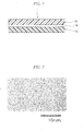
- FIG. 1 is a cross sectional view showing an example of the radio wave transmitting decorative film (hereinafter, simply referred to as decorative film) according to the present invention.
- the decorative film 1 includes a first polymer film 12, a light-reflecting layer 14 provided on the surface of the first polymer film 12, and a second polymer film 16 provided on the surface of the light-reflecting layer 14.
- a first polymer film 12 and a second polymer film 16 are films having radio wave transmissibility. At least one of the first polymer film 12 and second polymer film 16 is required to be a transparent film.
- the transmittance to visible light of the transparent polymer film is preferably 80% or more.
- the thickness of the polymer film is preferably 10 to 100 ⁇ m from the viewpoint of moldability of the decorative film 1.
- the thickness of the decorative film is preferably 20 to 150 ⁇ m.
- polystyrene film materials examples include polyolefin (polyethylene, polypropylene, an ethylene-propylene copolymer, an ethylene-vinyl acetate copolymer, or the like), cyclic polyolefin, modified polyolefin, polyvinyl chloride, polyvinylidene chloride, polystyrene, polycarbonate, poly-(4-methylpentene-1), an ionomer, an acrylic resin (polymethylmethacrylate, or the like), an acrylonitrile-butadiene-styrene copolymer (an ABS resin), an acrylonitrile-styrene copolymer (an AS resin), a butadiene-styrene copolymer, polyester (polyethylene terephthalate, polybutylene terephthalate, polycyclohexane terephthalate, or the like), polyphenylene oxide, modified polyphenylene oxide, polysulfone,
- polymer film materials may be used singly, or two or more types thereof may be combined and used as a copolymer, a blended product, a polymer alloy, or the like.
- the polymer film preferably include polycarbonate, polymethylmethacrylate, an AS resin, polystyrenes, cyclic polyolefins, polyethylene terephthalate, polybutylene terephthalate, and a modified product and a copolymer thereof and the like, from the viewpoint of transparency, strength, and moisture permeability,
- the polymer film materials preferably have the same materials as bases, from the viewpoint of incorporation with a base of a decorative member. Further, the polymer film may use a film having adhesive properties to the base of a decorative member. As the polymer film, a plurality of the polymer films may be laminated. During lamination, thermosetting adhesives or thermoplastic adhesives may be used. These polymer films may contain an additive if necessary. Examples of the additive include a strengthening agent, an antioxidant, an ultraviolet absorber, a lubricant, an anti-clouding agent, anti-fogging agent/misting agent, a plasticizer, a pigment, a near infrared absorber, an antistatic agent, and a colorant.
- the additive include a strengthening agent, an antioxidant, an ultraviolet absorber, a lubricant, an anti-clouding agent, anti-fogging agent/misting agent, a plasticizer, a pigment, a near infrared absorber, an antistatic agent, and a colorant.
- the light-reflecting layer 14 is formed by a physical vapor deposition of an alloy of silicon and a metal.
- an alloy composed of silicon and a metal the reflectance and brightness of the light-reflecting layer 14 are improved, as compared to the case where silicon is used alone, and thus a bright light-reflecting layer 14 can be obtained.
- the alloy is soft compared to silicon, internal stress of the light-reflecting layer 14 is reduced, thereby improving the adhesiveness with the first polymer film 12 and suppressing the occurrence of cracks.
- Silicon is a semiconductor material, unlike the metals described later. Silicon has the following properties, and thus is preferable in comparison to other semiconductor materials:
- Silicon may contain impurities which do not act as dopants, as long as the surface resistivity of the light-reflecting layer 14 can be maintained at a high level. It is preferable that silicon contains as few dopants (such as boron, phosphorus, arsenic and antimony) as possible. The amount of dopants is preferably 1 ppm or less, and more preferably 10 ppb or less.
- the metal a metal exhibiting a reflectance of 50% or higher is preferable.
- the metal include gold, silver, copper, aluminum, platinum, iron, nickel, and chromium, and the like, and aluminum and silver are preferred from the viewpoints of reflectance and cost, and aluminum is more preferable.
- the term "reflectance" refers to the diffuse reflectance including regular reflectance which is measured in accordance with condition d (n-D) of JIS Z 8722.
- the reflectance is measured including the regular reflection light of a gloss component using an integrating sphere and is calculated as an average of measured values across the visible light region, which ranges from the short wavelength side (i.e., 360 nm to 400 nm) to the long wavelength side (i.e., 760 nm to 830 nm).
- the proportion of the metal within the alloy (which is 100% in terms of volume) is preferably within a range from 0.1 to 70 volume %, and more preferably within a range from 40 to 70 volume%.
- the proportion of the metal is 0.1 volume % or more, brightness of the light-reflecting layer 14 increases and internal stress of the light-reflecting layer 14 also reduces.
- the proportion of the metal is 70 volume % or less, radio wave transmissibility improves even further.
- the alloy may contain impurities other than silicon and metals, as long as the surface resistivity and metallic gloss of the light-reflecting layer 14 can be maintained at a high level.
- the thickness of the light-reflecting layer 14 is preferably within a range from 10 to 500 nm, and more preferably within a range from 50 to 200 nm.
- the thickness of the light-reflecting layer 14 is 10 nm or more, it becomes difficult for light to pass therethrough, and thus a sufficient metallic gloss can be attained.
- the thickness of the light-reflecting layer 14 is 500 nm or less, an increase in the electrical conductivity is suppressed, and thus a satisfactory level of radio wave transmissibility can be maintained.
- increase in the internal stress of the light-reflecting layer 14 can be suppressed, thereby the warping and deformation of decorative members, occurrence of cracks, delamination or the like, can be suppressed.
- the light-reflecting layer 14 When the light-reflecting layer 14 is thin, the light is passed through and the reflectance reduces, and thus a dark metallic gloss can be obtained. Therefore, brightness of the metallic gloss can be adjusted by changing the thickness of the light-reflecting layer 14.
- the thickness of the light-reflecting layer 14 can be measured from high resolution microscopic images of the cross section of the light-reflecting layer 14.
- the surface resistivity of the light-reflecting layer 14 is preferably 10 3 ⁇ or higher, more preferably 10 6 ⁇ or higher. When the surface resistivity of the light-reflecting layer 14 is 10 3 ⁇ or higher, a satisfactory level of radio wave transmissibility can be maintained.
- the surface resistivity of the light-reflecting layer 14 is measured by a four-pin probe method in accordance with JIS K7194.
- the average surface roughness of the light-reflecting layer 14 is preferably 0.05 ⁇ m or less. When the average surface roughness of the light-reflecting layer 14 is 0.05 ⁇ m or less, irregular reflection is suppressed, and thus a sufficient metallic gloss can be attained.
- the lower limit for the average surface roughness of the light-reflecting layer 14 is set to 0.1 nm, which can be achieved with a polishing process.
- the average surface roughness of the light-reflecting layer 14 refers to an arithmetic average roughness Ra determined in accordance with JIS B 0601-2001.
- a surface profile of the light-reflecting layer is measured by an atomic force microscope, and a reference length is extracted in the direction of the average line, followed by the determination of an average value (i.e., arithmetic average roughness Ra) derived from the sum of the absolute values of deviations ranging from the average line in which the reference length is extracted, to the roughness curve.
- an average value i.e., arithmetic average roughness Ra
- the average surface roughness of the light-reflecting layer 14 is affected by the average surface roughness of the first polymer film 12. Therefore, the average surface roughness of the first polymer film 12 is preferably 0.5 ⁇ m or less, and more preferably 0.1 ⁇ m or less. When the average surface roughness is 0.5 ⁇ m or less, even though the light-reflecting layer 14 is thin, the light-reflecting layer is dependent on the surface of the first polymer film 12, and thus a sufficiently mirror-like metallic gloss is attained.
- the average surface roughness of the first polymer film 12 refers to an arithmetic average roughness Ra determined in accordance with JIS B 0601-2001.
- the light-reflecting layer may be provided on both sides of the first polymer film. At this time, one side of the light-reflecting layer is thin so that flexibility can be increased, and metallic gloss can be increased.
- the light-reflecting layer 14 is formed by physical vapor deposition of an alloy of silicon and a metal.
- the physical vapor deposition process is a method for forming a thin film by vaporizing an evaporation material (an alloy) in a vacuum vessel in some way and then depositing the vaporized evaporation material on top of the substrate placed nearby, and the process can be classified into an evaporation system and a sputtering system, depending on the method for vaporizing an evaporation material.
- Examples of the evaporation system include an electron beam (EB) deposition process, an ion plating process, and a pulse laser deposition process and examples of the sputtering system include a radiofrequency (RF) sputtering process, a magnetron sputtering process, an opposite target type magnetron sputtering process, and ECR sputtering, and the like.
- EB electron beam
- ion plating process an ion plating process
- sputtering system include a radiofrequency (RF) sputtering process, a magnetron sputtering process, an opposite target type magnetron sputtering process, and ECR sputtering, and the like.
- RF radiofrequency
- an EB deposition process tends to form a porous film having an unsatisfactory level of film strength, it is characterized in that damage inflicted on the substrate is minimal.
- An ion plating process is preferred because a film having an intense adhesive force can be obtained.
- a magnetron sputtering process is preferred because a film can be grown at a high growth rate, an opposite target type magnetron sputtering process is preferred because a thin film can be formed without causing plasma damage to the substrate, and an RF sputtering process is preferred because a target (evaporation material) with high resistance can be used.
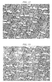
- FIG. 2 is a high resolution transmission electron microscope image of the surface of a light-reflecting layer formed by a DC magnetron sputtering process using a silicon-aluminum alloy. It can be seen that unlike the assembly of independent islands (microclusters) observed in conventional cases where indium, tin, or the like is used, no gap is present where the alloy is absent, as a result of which a continuous layer having a homogeneous amorphous structure is formed.
- FIG. 3 is a cross sectional view showing another example of a radio wave transmitting decorative film according to the present invention.
- a decorative film 1 includes a first polymer film 12, an adhesion promoting layer 20 provided on the surface of the first polymer film 12, a light-reflecting layer 14 provided on the surface of the adhesion promoting layer 20, and a second polymer film 16 provided on the surface of the light-reflecting layer 14.
- the same configurations as in the first embodiment have the same references, the description of which will be omitted.
- the adhesion promoting layer 20 is previously formed on the surface of the polymer film before forming the light-reflecting layer 14 or on the surface of the light-reflecting layer 14 after forming the light-reflecting layer 14.
- the materials for the adhesion promoting layer 20 preferably have radio wave transmissibility or optical transparency, and adhesive force to polymer film, and is capable of forming covalent, coordination, or hydrogen bonds to the light-reflecting layer.
- the materials include an adhesion promoter, an inorganic matter, and a composite of an adhesion promoter and an inorganic matter, and the like.
- the adhesion promoting layer 20 includes (a) a layer formed of adhesion promoters, (b) a layer formed of inorganic matter, (c) a layer formed of composite of adhesion promoters and inorganic matter, (d) a layer formed by performing a physical or chemical surface treatment on the surface of the polymer film, and the like.
- the adhesion promoter includes a resin (hereinafter, referred to as polar resin) having a polar bond (ester bond, urethane bond, allophanate bond, urea bond, burette bond, amide bond, and the like) or a polar group (a hydroxyl group, a carboxyl group, an amino group, an isocyanate group, an oxazoline group, a mercapto group, an epoxy group, and the like), in the main chain or a side chain.
- the polar resin include nitrocellulose, acrylic resin, urethane resin, polyphosphazene, polyamide, epoxy resin, and the like.
- the adhesion promoter may further contain a silane coupling agent.
- silane coupling agent examples include vinyltriethoxysilane, vinyltris (2-methoxyethoxy) silane, 3- methacryloxypropyltrimethoxysilane, 3-glycidoxypropyltrimethoxysilane, 2-(3,4-epoxycyclohexyl)ethyltrimethoxysilane, N-2-(aminoethyl)3-aminopropyltrimethoxysilane, N-2-(aminoethyl)3-aminopropylmethydimethoxysilane, 3-aminopropyltriethoxysilane, N-phenyl-3-aminopropyltrimethoxysilane, 3-mercaptopropyltrimethoxysilane, 3-chloropropyltrimethoxysilane, cyanoethyltrimethoxysilane, cyanopropyltrimethoxysilane, and the like.
- Transparent colorants
- Examples of the inorganic matter include metal oxide, and preferably silicon oxide or titanium oxide.
- the metal oxide preferably has a particle shape.
- the average particle diameter of the metal oxide is preferably 5 to 1000 nm.
- Composites of the adhesion promoter and inorganic matter include (c1) metal oxide blended with an adhesion promoter, (c2) an organic and inorganic hybrid where metal alkoxide is blended with an adhesion promoter, followed by dealcohol condensation, and thus metal oxide is aggregated and precipitated in the adhesion promoter, and (c3) an organic and inorganic hybrid where polar resin (epoxy resin, acrylic resin, polyamide, or the like) having a metal alkoxy group in a side chain is subjected to dealcohol condensation and thus metal oxide is aggregated and precipitated in a polar resin, and the like. From the viewpoint of covalent bonding of a metal oxide and a polar resin as an adhesion promoter, (c3) is preferable.
- dealcohol condensation is preferably performed after forming the light-reflecting layer 14.
- metal oxide is aggregated and precipitated by dealcohol condensation, metal oxide can be disposed across the whole surface of the polymer film to improve adhesive force and reflectance.
- a proportion of the metal oxide in the composite is preferably 15 to 70% by volume in terms of the solid content.
- the adhesion promoting layer 20 contains metal oxide
- the following effect is attained.
- the light-reflecting layer 14 is formed by physical vapor deposition on the surface of the polymer film, ions of elements (silicon, aluminum, or the like) forming the light-reflecting layer 14 infiltrate and are embedded in the polymer film from the interface. Therefore, the interface of the polymer film and the light-reflecting layer 14 is irregular, and the area of the interface is extraordinarily increased. As a result, the reflectance of incident light to the light-reflecting layer 14 from the surface of polymer film become lower than that for incident light to the surface of the light-reflecting layer 14 on the opposite side of the polymer film. Accordingly, a transparent hard metal oxide is disposed on the interface of the polymer film and the light-reflecting layer 14, and thus, infiltration and embedding of ions to the polymer film can be suppressed.
- a surface treatment is one where the surface of a polymer film is roughened, or actively reacted with a gas such as oxygen to form an oxygen complex such as a hydroxyl group, a ketone group, or highly reactive polar group such as an amine group.
- a surface treatment may be a blast treatment, chemical conversion treatment, corona discharge treatment, ultraviolet treatment, electron beam treatment, plasma treatment, or the like.
- FIG. 4 is a cross sectional view showing another example of the radio wave-transmitting decorative film of the invention.
- the decorative film 1 includes a first polymer film 12, a light-reflecting layer 14 provided on the surface of the first polymer film 12, an adhesion promoting layer 20 provided on the surface of the light-reflecting layer 14, and a second polymer film 16 provided on the surface of the adhesion promoting layer 20.
- the same configurations as the first embodiment and the second embodiment have the same references, the description of which will be omitted.
- FIG. 5 is a cross sectional view showing other examples of the radio wave-transmitting decorative film of the invention.
- the decorative film 1 includes a first polymer film 12, an adhesion promoting layer 20 provided on the surface of the first polymer film 12, a light-reflecting layer 14 provided on the surface of the adhesion promoting layer 20, an adhesion promoting layer 20 provided on the surface of the light-reflecting layer 14, and a second polymer film 16 provided on the surface of the adhesion promoting layer 20.
- the same configurations as the first embodiment and the second embodiment have the same references, the description of which will be omitted.
- FIG. 6 is a cross sectional view showing other examples of the radio wave-transmitting decorative film of the invention.
- the decorative film 1 includes a first polymer film 12, an adhesion promoting layer 20 provided on the surface of the first polymer film 12, a design portion 18 provided on a portion of the surface of the adhesion promoting layer 20, a light-reflecting layer 14 provided on the surface of the adhesion promoting layer 20 and the design portion 18, and a second polymer film 16 provided on the surface of the light-reflecting layer 14.
- the same configurations as the first embodiment and the second embodiment have the same references, the description of which will be omitted.
- Design portion 18 is a portion (character, symbol, figure, pattern, or the like) where materials with an occlusion property (optical non- transmissibility or optical low transmissibility) are placed and formed into a desirable pattern shape.
- a metallic gloss is formed as a background, and characters (Japanese characters, alphabet, numbers, and the like), symbols, or the like are depicted.
- the design portion 18 can be formed by printing using a known printing ink or paint.
- the decorative film 1 has a flat shape, however when a decorative member is produced using the film, it is required to make three-dimensional shape, and the decorative film 1 is partially stretched.
- the light-reflecting layer 14 is dependent on the shape of the decorative member, but cracking may occur unexpectedly which is observable visually and the external appearance is deteriorated depending on degree or direction of stretching. Therefore, a number of nano-level irregular sites are previously provided in the light-reflecting layer 14, the adhesion promoting layer 20, or the polymer film, and the light-reflecting layer 14 is divided and broken by a portion where the irregular sites are provided when the decorative film 1 is stretched, and thus a crack large enough to be observed visually and deterioration of the external appearance can be suppressed.
- the divided light-reflecting layer 14 can be recognized as gloss which is observed visually and thus the size is about 5 ⁇ m or less.
- the distance between the divided light-reflecting layers 14 is stretched and enlarged, it is recognized that reflectance is lowered, which is observed visually, and the light-reflecting layer become thin.
- irregular sites include the following examples.
- the irregular site of ( ⁇ ) is hard and brittle, and thus the light-reflecting layer 14 is divided and broken by the irregular site.
- the irregular site of ( ⁇ ) has low adhesion strength between the polymer film and the light-reflecting layer 14, and thus when the decorative film 1 is stretched, the light-reflecting layer 14 cannot follow the stretching, and thus the light-reflecting layer 14 is divided and broken by the irregular site.
- the irregular site of (y) has a low elastic modulus of the adhesion promoting layer 20, and thus when the decorative film 1 is stretched, the adhesion promoting layer 20 is simultaneously stretched, the light-reflecting layer 14 cannot follow the stretching, and thus the light-reflecting layer 14 is divided and broken by the irregular site.
- the adhesion promoting layer 20 around the irregular site of ( ⁇ ) has a high elastic modulus, and thus when the decorative film 1 is stretched, the adhesion promoting layer 20 is not stretched, and therefore the light-reflecting layer 14 is not divided and broken by the irregular site.
- the irregular site of ( ⁇ ) can be formed by hardening a portion of silicon and a metal on the light-reflecting layer 14 at the nano level.
- a portion of the light-reflecting layer 14 is formed into ceramics by reacting gas containing a typical non-metallic element with silicon and a metal and thus can form an irregular site.
- the typical non-metal element include nitrogen, carbon, oxygen, boron, phosphorus, and sulfur. From the viewpoint of easy handling of gas and the influence of reaction products, nitrogen, oxygen, and carbon are preferable.
- the nitrogen-containing gas include molecular nitrogen.
- the oxygen-containing gas include molecular oxygen.
- the carbon-containing gas include hydrocarbons.
- a ceramics-forming degree is preferably 0.01 mol% to 10 mol% of the light-reflecting layer 14.
- the ceramics-forming degree is less than 0.01 mol%, the number of irregular sites is insufficient and cracking easily occurs, which can be observed visually.
- the ceramics-forming degree is more than 10 mol%, whiteness and transparency due to formation of ceramics are increased and an unsatisfactory level of metallic gloss easily occurs.
- the ceramics-forming degree is dependent on the size of vacuum chamber and the deposition rate, but the flow rate of typical non-metal gas can be adjusted in the range of 0.1 to 50 sccm.
- the surface of the polymer film can be subjected to a hydrophilic process by flowing oxygen or nitrogen, which is preferable from the viewpoint of adhesiveness.
- Ceramics-forming analysis (confirmation of irregular site) can be performed by an X-ray diffraction apparatus.
- the irregular site of ( ⁇ ) and/or ( ⁇ ) can be formed by (I) to (V).
- the adhesion promoting layer 20 is formed using (a) an adhesion promoter.
- a minute nucleus can be formed using a dry process as a basis. For example, a monomer, oligomer or polymer having a polar group is heated and deposited, and thereby a minute portion which is formed of a resin having a polar group is homogeneously distributed, to form an irregular site of ( ⁇ ). At this time, the distribution density can be adjusted by changing the deposition amount.
- the surface of the polymer film is subjected to a surface treatment such as atmospheric plasma treatment or corona discharge treatment to introduce a polar group, and then an aqueous solution of a polar group-containing resin is thinly coated to bond the polar group-containing resin to a polar group of the surface of the polymer film by hydrogen bonding and the like, the polar group-containing resin is fixed, and thus a minute portion which is formed of the polar group-containing resin is distributed homogeneously to form an irregular site of ( ⁇ ).
- a surface treatment such as atmospheric plasma treatment or corona discharge treatment to introduce a polar group
- an aqueous solution of a polar group-containing resin is thinly coated to bond the polar group-containing resin to a polar group of the surface of the polymer film by hydrogen bonding and the like, the polar group-containing resin is fixed, and thus a minute portion which is formed of the polar group-containing resin is distributed homogeneously to form an irregular site of ( ⁇ ).
- a minute portion of crosslinked polyolefin which homogeneously distributes a hydrocarbon such as methane without a polar group by plasma polymerization and the like is formed on the surface of the polymer film, which is used as a mask, and the aqueous solution described above is coated to distribute a minute portion which is formed of the polar group-containing resin homogeneously, to form an irregular site of ( ⁇ ).
- a hydrophilic property is provided by a partial plasma process and the like or a lipophilic property is provided by chemical vapor deposition of crosslinked polyolefin, and then an aqueous silane coupling solution is coated, and a minute portion having partially high affinity is distributed homogeneously to form an irregular site of ( ⁇ ).
- the adhesion promoting layer 20 is formed using (b) the inorganic matter.
- a minute nucleus can be formed using a dry process as a basis.
- inorganic matter when inorganic matter is physically or chemically deposited, a minute portion formed of the inorganic matter is distributed homogeneously by controlling the density of the deposition amount.
- An adhesion strength difference between a portion of inorganic matter (metal oxide particles, or the like) and a portion (resin, or the like) around the inorganic matter occurs, and thus a minute portion having a high adhesion strength and a minute portion having a low adhesion strength are distributed homogeneously, to form an irregular site of ( ⁇ ).
- an elastic modulus difference between a portion of inorganic matter (metal oxide particles, or the like) and a portion (resin, or the like) around the inorganic matter occurs, and thus a fine portion having a high elastic modulus and a minute portion having a low elastic modulus are distributed homogeneously, to form an irregular site of (y) as well.
- inorganic matter be adhered well to the polymer film.
- Examples of methods for improving the adhesive force between the inorganic matter and the polymer film include a surface treatment method on the surface of polymer film; a method where a bias voltage is applied so that the inorganic matter is accelerated to a high energy and hits the polymer film, in a case of forming fine inorganic matter by a physical or chemical vapor deposition; a method where DLC (diamond-like carbon) or silicon and the like-containing DLC and the like is formed by a PBII (plasma based ion implantation) method and the like, in a case of forming fine inorganic matter by a chemical polymerization method; and the like.
- a chemical polymerization method adhesion density can be changed depending on polymerization conditions, and thus fine inorganic matter which is distributed homogeneously can be formed.
- the adhesion promoting layer 20 is formed using (c) a composite of an adhesion promoter and inorganic matter.
- a minute nucleus can be formed using a dry process as a basis. Specifically, this can be formed similarly to (II) or (III).
- (IV) Having minute portion of different elastic modulus on the surface of the polymer film has the same effect as the adhesion promoting layer 20 formed by (III).
- it may be a copolymer having a soft segment and a hard segment which can utilize a polymer film where the hard segment portion is microphase-separated as an island shape.
- the copolymer include polyester, polyolefin, a polyamide thermoplastic elastomer; a silicon polyimide copolymer, or the like.
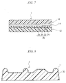
- FIG. 7 is a cross sectional view of decorative film 1 schematically showing a minute portion 22 having high adhesion strength or elastic modulus and a minute portion 24 (irregular site) having a low adhesion strength or elastic modulus which are alternately formed in adhesion promoting layer 20.
- the light-reflecting layer 14 is subdivided by the portion 24 having low adhesion strength or elastic modulus.
- FIG. 8 is a cross sectional view showing one example of the decorative member of the invention.
- the decorative member 2 is one where a decorative film 1 is incorporated into the surface of a base 30 having a plurality of convex portions along a form of the base 30.
- a base 30 is a molded body of materials having radio wave transmissibility.
- radio wave-transmitting materials include an insulating organic material.
- the term "insulating" means a surface resistivity of 10 6 ⁇ or higher, and the surface resistivity is preferably 10 8 ⁇ or higher.
- the surface resistivity of a substrate is measured by a four-pin probe method in accordance with JIS K7194.
- the material with radio wave transmissibility is preferably an insulating organic material from the viewpoint of molding processability.
- organic material examples include polyolefin (polyethylene, polypropylene, ethylene-propylene copolymer, ethylene-vinyl acetate copolymer, or the like), cyclic polyolefin, modified polyolefin, polyvinyl chloride, polyvinylidene chloride, polystyrene, polyamide (nylon 6, nylon 46, nylon 66, nylon 610, nylon 612, nylon 11, nylon 12, nylon 6-12, nylon 6-66, or the like), polyimide, polyamideimide, polycarbonate, poly-(4-methylpentene-1), an ionomer, an acrylic resin (polymethylmethacrylate, or the like), an ABS resin, an AS resin, a butadiene-styrene copolymer, polyoxymethylene, polyvinyl alcohol, an ethylene-vinyl alcohol copolymer, polyester (polyethylene terephthalate, polybutylene terephthalate, polycyclohexane terephthalate
- organic materials may be used alone, or two or more types thereof may be combined and used as a copolymer, a blended product, a polymer alloy, a laminated body, or the like.
- These organic materials may contain an additive if necessary.
- the additive include a strengthening agent, an antioxidant, an ultraviolet absorber, a lubricant, an an anti-clouding agent, anti-fogging agent/misting agent, a plasticizer, a pigment, a near infrared absorber, an antistatic agent, and a colorant, and the like.
- a decorative member 2 can be produced by forming a decorative film 1 into a desirable shape, then setting in a mold having the same shape, and injecting a liquid resin from an opening portion of the mold to form incorporated matter.
- a polymer film of the base 30 side of the decorative film 1 may use the same resins as the base 30 and attain good adhesiveness (not shown). Each corner portion of convex portion of the base 30 is particularly stretched, and a light-reflecting layer in the decorative film 1 is subdivided into many minute portions (not shown).
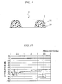
- FIG. 9 is a cross-sectional view showing another example of a decorative member of the invention.
- the decorative member 2 of decorative film 1 is incorporated into the surface of base 30 having a doughnut-like shape, along a form of the base 30.
- the heated decorated film 1 using an adhesive film 32 is incorporated into the base 30 formed above.
- the same configuration as the seventh embodiment has the same references, the description of which will be omitted.
- Each corner portion of convex portion of the base 30 is particularly stretched, and a light-reflecting layer in the decorative film 1 is subdivided into many minute portions (not shown).
- the decorative film of the invention and decorative member using the same described above is formed by a physical vapor deposition of an alloy of silicon and a metal and has a bright light-reflecting layer with high reflectance, and therefore it has radio wave transmissibility and the same metallic gloss as chromium plating. Moreover, since an alloy of silicon and a metal which is chemically stable in comparison to indium and tin and the like are used, the loss of metallic gloss is less likely to occur over time. In addition, the light-reflecting layer is protected with the polymer film, and the loss of metallic gloss is less likely to occur. Moreover, because an alloy composed of silicon and a metal is used which is cheaper than rare metal simple substances such as indium, the production cost is low.
- the number of laminations of decorative film is small, and thus the production cost is low.
- the decorative film since the light-reflecting layer is sandwiched between two polymer films, the decorative film has excellent stretch moldability, and the decorative member using the same has excellent external appearance property in the corner portion.
- the adhesion promoting layer or the polymer film has a number of irregular sites, stretch moldability of the decorative film is increased, and the decorative member using the same has an improved external appearance property at the corner portion.
- the conductive metal element is fixed by semi-conductive silicon to the light-reflecting layer, performance of radio wave transmissibility without partially connecting islands such as indium with each other, which has been found in a decorative member using conventional decorative film due to the pressure and the like in molding does not need to be examined, and has high productivity.
- the reason why an alloy composed of silicon and a metal is used is as follows. Although silicon exhibits a high reflectance in the visible light region, it is lower than the reflectance of metals (for example, 98% reflectance for silver and 90% reflectance for aluminum at a wavelength of 620 nm, according to the value described in " Handbook of Optical Constants of Solids", edited by E. L. Palik (Academic Press, 1985 )), which is 36% (at a wavelength of 620 nm, according to the value described in the Handbook).
- the reflectance can be improved and the brightness can be enhanced, thereby obtaining a light-reflecting layer exhibiting metallic gloss equal to or greater than bright chromium plating.
- the metal is soft compared to silicon, internal stress of the light-reflecting layer is reduced, thereby improving the adhesiveness thereof and suppressing the occurrence of cracks.
- the term "reflectance” refers to the diffuse reflectance including the regular reflectance which is measured in accordance with Condition d (n-D) of JIS Z 8772.
- the reflectance was measured including the regular reflection light of a gloss component using an integrating sphere. More specifically, the reflectance of a decorative member was measured including the regular reflection light of gloss component using an integrating sphere, by use of an ultraviolet visible near infrared spectrophotometer (manufactured by JASCO Corporation under the trade name of V-570). An average of the values collected from 401 points of measurement that were present across a region ranging from a wavelength of 380 nm to 780 nm was then determined.
- the transmissibility of a decorative member was measured, by the use of an integrating sphere, using an ultraviolet visible near infrared spectrophotometer (manufactured by JASCO Corporation under the trade name of V-570).
- the thickness of a light-reflecting layer was measured at five points by observing a cross section of the light-reflecting layer using a transmission electron microscope (manufactured by JEOL Ltd., under the trade name of JEM-4000EX), and the measured values were averaged.
- the average surface roughness was determined by scanning 1 ⁇ m 2 of the surface of a sample using a scanning probe microscope (manufactured by SII NanoTechnology Inc. under the trade name of SPA400) with DFM mode of atomic force microscope, followed by the production of an image of the surface profile. It was measured immediately after forming a light-reflecting layer.
- the surface resistivity of a sample was measured by placing a series 4-pin probe (ASP) on top of a sample using a resistivity meter (Loresta GP, Model MCP-T600, manufactured by Dia Instruments Co., Ltd., in accordance with JIS K7194). The measurement voltage was set to 10 V. It was measured immediately after forming a light-reflecting layer.
- ASP 4-pin probe
- An Elastic modulus difference of a minute portion on the surface of the adhesion promoting layer or the polymer film was determined as follows. A viscoelastic distribution on the surface of the adhesion promoting layer or the polymer film from flexural oscillation of a perceiving lever was imaged and an elastic modulus difference of a minute portion was observed using a scanning probe microscope (manufactured by SII NanoTechnology Inc. under the trade name of SPA400) with a micro-viscoelastic measuring mode.
- the surface of the light-reflecting layer was observed using an electron scanning microscope (manufactured by JASCO Corporation under the trade name of JSM6390LV). Since making the surface of the sample conductive and a grounding process were not performed, the decorative film was largely stretched, and a portion where resistance of light-reflecting layer was increased could not be imaged.
- acryl film as a first polymer film 12, having a thickness of 50 ⁇ m, was subjected to physical vapor deposition using a DC sputtering apparatus with the following target to form a light-reflecting layer 14.
- An alloy composed of silicon and aluminum which was doped with boron (aluminum proportion: 60 volume %, amount of doped boron: approximately 10 -7 mol%) was used as the target.
- the reflectance of the elemental form of aluminum is 87.6%.
- acryl film, as a second polymer film 16 having a thickness of 50 ⁇ m was subjected to thermal lamination on the surface of the light-reflecting layer 14 to obtain a decorative film 1 shown in FIG. 1 .
- the thickness of the light-reflecting layer 14 the amounts of transmission attenuation (S21) at 1 GHz and 3 GHz, the reflectance of visible light entered from first polymer film 12, the surface resistivity, and the average surface roughness were measured.
- the external appearance of the decorative film 1 was observed.
- the proportion of aluminum in the light-reflecting layer 14 was the same as the proportion of aluminum in the target.
- Table 1 a graph indicating the amount of transmission attenuation (S21) and amount of reflection attenuation (S11) of radio waves of the radio wave-transmitting decorative film 1 is shown in FIG. 10 .
- a graph indicating the reflectance of the decorative film 1 is shown in FIG.
- a decorative film was observed in a manner similar to Example 1, except that elemental silicon was used as the target.
- the thickness of the light-reflecting layer, the amounts of transmission attenuation (S21) at 1 GHz and 3 GHz, the reflectance, the surface resistivity, and the average surface roughness were measured.
- the external appearance of the decorative film was observed. The results are shown in Table 1.
- the surface of polycarbonate film having a thickness of 100 ⁇ m as a first polymer film 12 was subjected to physical vapor deposition at a flow of nitrogen gas of 0.5 sccm, to form a light-reflecting layer 14 of which a portion was formed into ceramics, using a DC sputtering apparatus with the same target as Example 1. Then, a polyolefin chloride layer was laminated on the surface of black ABS film having a thickness of 100 ⁇ m as a second polymer film 16 and the polyolefin chloride layer was used as an adhesive, which was adhered to light-reflecting layer 14 to obtain a decorative film 1.
- the thickness of the light-reflecting layer 14 the amounts of transmission attenuation (S21) at 1 GHz and 3 GHz, the reflectance, the surface resistivity, and the average surface roughness were measured.
- the external appearance of the decorative film 1 was observed.
- the results are shown in Table 1.
- the decorative film 1 was made as a preform in a mold, ABS resin was injected into a mold, and decorative film 1 and base 30 were incorporated as shown in FIG. 8 to obtain a decorative member 2.
- the external appearance of the decorative member 2 in particular, the metallic gloss of the corner portion of a convex portion was observed. The result is shown in Table 1.
- oxygen plasma processing was performed under conditions of power: 500 W, time: 2 minutes, reaching vacuum degree: 6 ⁇ 10 -1 Pa, oxygen flow rate: 15 sccm.
- physical vapor deposition was performed using an alloy (aluminum proportion: 70 volume%) of silicon and aluminum by a DC sputtering apparatus as a target, to form a light-reflecting layer 14. Black ABS film was adhered in a manner similar to Example 2, to obtain a decorative film 1.
- the thickness of the light-reflecting layer 14 the amounts of transmission attenuation (S21) at 1 GHz and 3 GHz, the reflectance, the surface resistivity, and the average surface roughness were measured.
- the external appearance of the decorative film 1 was observed.
- the results are shown in Table 1.
- the decorative film 1 was made as a preform in a mold, ABS resin was injected into a mold, and decorative film 1 and base 30 were incorporated as shown in FIG. 8 to obtain a decorative member 2.
- the external appearance of the decorative member 2 in particular, the metallic gloss of the corner portion of a convex portion was observed. The result is shown in Table 1.
- a polyester thermoplastic elastomer film (manufactured by Toray corporation, trade name Hytrel, using aromatic polyester as a hard segment and polyetherester as a soft segment) having a thickness of 125 ⁇ m was prepared as a first polymer film.
- the elastic modulus of the surface of the film was measured, and a minute portion having a high elastic modulus and a minute portion (irregular site) having a low elastic modulus were distributed homogeneously, which was confirmed.
- the surface of the film was subjected to an oxygen plasma process in a manner similar to Example 3.
- the thickness of the light-reflecting layer 14, the amounts of transmission attenuation (S21) at 1 GHz and 3 GHz, the reflectance, the surface resistivity, and the average surface roughness were measured.
- the external appearance of the decorative film 1 was observed.
- Table 2 As shown in FIG. 9 , the decorative film 1 was incorporated into a base 30 formed of polybutylene terephthalate by pressure molding using a polyolefin chloride layer provided for the first polymer film 12 side of the decorative film 1 as an adhesive to obtain a decorative member 2.
- the external appearance of the decorative member 2 in particular, the metallic gloss of the corner portion of a convex portion was observed. The result is shown in Table 2.
- a laminate of a copolymerizable polyester film (manufactured by Toyobo Co., Ltd., trade name Softshine) having a thickness of 25 ⁇ m and a polycarbonate film having a thickness of 50 ⁇ m were prepared as a first polymer film.
- chemical vapor deposition was performed using silicon-containing DLC in PBII apparatus (manufactured by Cup-kurita Corporation), and a number of hard minute portions were formed to set as an adhesion promoting layer 20. Further, oxygen plasma processing was performed under conditions of power: 250 W, time: 1 minute, reaching vacuum degree: 6 ⁇ 10 -1 Pa, oxygen flow rate: 15 sccm.
- the elastic modulus of the surface of the adhesion promoting layer 20 was measured, and a minute portion having a high elastic modulus and a minute portion (irregular site) having a low elastic modulus were distributed homogeneously, which was confirmed.
- physical vapor deposition was performed using an alloy (aluminum proportion: 55 volume%) of silicon and aluminum by a DC sputtering apparatus as a target, to form a light-reflecting layer 14. Black ABS film was adhered in a manner similar to Example 2, to obtain a decorative film 1.
- the thickness of the light-reflecting layer 14, the amounts of transmission attenuation (S21) at 1 GHz and 3 GHz, the reflectance, the surface resistivity, and the average surface roughness were measured.
- the external appearance of the decorative film 1 was observed.
- Table 2 As shown in FIG. 9 , the decorative film 1 was incorporated into a base 30 formed of ABS resin by pressure molding to obtain a decorative member 2 using a polyolefin chloride layer provided for the first polymer film 12 of decorative film 1 as an adhesive to obtain a decorative member 2.
- the external appearance of the decorative member 2 in particular, the metallic gloss of the corner portion of a convex portion was observed. The result is shown in Table 2.
- Example 4 Thickness of the light-reflecting layer (nm) 75 150 Average surface roughness of the light-reflecting layer (nm) 2.3 1.9 Amount of transmission attenuation (dB) 0.0 0.0 0.0 0.1 1GHz 3GHz Reflectance (%) 58.1 57.6 400 nm 59.7 57.9 500 nm 60.6 58.2 600 nm 61.2 58.4 700 nm 59.9 58.0 Average value Surface Resistivity ( ⁇ ) 10 8 or more 10 8 or more External appearance of decorative film Metallic gloss Metallic gloss External appearance of decorative member In metallic luster, significant change is not shown. In metallic luster, significant change is not shown.
- the invention is useful as metallic luster of decorative members, in particular, a decorative film using the same used in the casing of a mobile phone; the button of a switch; the casing of a watch; and the radiator grill, bumper, panel or the like of a vehicle.
Landscapes
- Chemical & Material Sciences (AREA)
- Chemical Kinetics & Catalysis (AREA)
- Engineering & Computer Science (AREA)
- Materials Engineering (AREA)
- Mechanical Engineering (AREA)
- Metallurgy (AREA)
- Organic Chemistry (AREA)
- Laminated Bodies (AREA)
- Physical Vapour Deposition (AREA)
Claims (5)
- Radiowellen übertragende Dekorfolie, umfassend:einen ersten Polymerfilm; undeinen zweiten Polymerfilm; undeine Licht reflektierende Schicht, die zwischen dem ersten Polymerfilm und dem zweiten Polymerfilm angeordnet ist und durch physikalische Dampfabscheidung einer Legierung aus Silizium und einem Metall gebildet ist.
- Radiowellen übertragende Dekorfolie nach Anspruch 1, wobei das Metall einen höheren Reflexionsgrad als Silizium hat.
- Radiowellen übertragende bekorfolie nach Anspruch 1. oder 2, wobei das Metall Aluminium ist.
- Radiowellen übertragende Dekorfolie nach einem der Ansprüche 1 bis 3, die ferner eine Adhäsion fördernde schicht zwischen dem ersten Polymerfilm oder dem zweiten Polymerfilm und der Licht reflektierenden Schicht umfasst.
- Dekorgegenstand, der die Radiowellen übertragende Dekorfolie nach einem der Ansprüche 1 bis 3 auf der Oberfläche einer Basis umfasst.
Applications Claiming Priority (2)
| Application Number | Priority Date | Filing Date | Title |
|---|---|---|---|
| JP2009064568A JP5346632B2 (ja) | 2009-03-17 | 2009-03-17 | 電波透過性加飾フィルムおよびこれを用いた装飾部材 |
| PCT/JP2010/001826 WO2010106778A1 (ja) | 2009-03-17 | 2010-03-15 | 電波透過性加飾フィルムおよびこれを用いた装飾部材 |
Publications (3)
| Publication Number | Publication Date |
|---|---|
| EP2409832A1 EP2409832A1 (de) | 2012-01-25 |
| EP2409832A4 EP2409832A4 (de) | 2013-02-27 |
| EP2409832B1 true EP2409832B1 (de) | 2013-08-21 |
Family
ID=42739446
Family Applications (1)
| Application Number | Title | Priority Date | Filing Date |
|---|---|---|---|
| EP10753275.6A Not-in-force EP2409832B1 (de) | 2009-03-17 | 2010-03-15 | Radiowellen übertragender schmuckfilm und schmuckelement damit |
Country Status (5)
| Country | Link |
|---|---|
| US (1) | US9493870B2 (de) |
| EP (1) | EP2409832B1 (de) |
| JP (1) | JP5346632B2 (de) |
| CN (1) | CN102395462B (de) |
| WO (1) | WO2010106778A1 (de) |
Families Citing this family (27)
| Publication number | Priority date | Publication date | Assignee | Title |
|---|---|---|---|---|
| CN102638953B (zh) * | 2012-04-13 | 2016-02-03 | 深圳光启创新技术有限公司 | 一种无线通信装置的保护壳 |
| JP6291156B2 (ja) * | 2012-04-23 | 2018-03-14 | マクセル株式会社 | 樹脂製エンコーダスケール、エンコーダ、樹脂製エンコーダスケールの製造方法およびエンコーダの製造方法 |
| KR101548158B1 (ko) | 2012-09-07 | 2015-08-28 | 제일모직 주식회사 | 성형품 및 성형품의 제조 방법 |
| JP6186684B2 (ja) * | 2012-09-18 | 2017-08-30 | 日本電気株式会社 | 加飾フィルム、それを備えた筐体及びその製造方法 |
| KR20140087802A (ko) | 2012-12-31 | 2014-07-09 | 제일모직주식회사 | 복합재 및 상기 복합재의 제조 방법 |
| JP6162425B2 (ja) * | 2013-02-25 | 2017-07-12 | アイカ工業株式会社 | 金属調化粧板 |
| JP6366134B2 (ja) * | 2014-07-23 | 2018-08-01 | Dic株式会社 | 電磁波送受信機器用カバー |
| JP6665781B2 (ja) * | 2014-08-21 | 2020-03-13 | ソニー株式会社 | 筐体部品、電子機器、筐体部品の製造方法 |
| EP3255965B1 (de) | 2015-02-03 | 2022-06-15 | Sony Group Corporation | Gehäusekomponente, elektronische vorrichtung und verfahren zur herstellung der gehäusekomponente |
| TW201722704A (zh) | 2015-10-15 | 2017-07-01 | 聖高拜塑膠製品公司 | 季節性太陽能控制複合物 |
| JP6656760B2 (ja) * | 2016-05-31 | 2020-03-04 | 株式会社吉野工業所 | 加飾成形品 |
| US10873129B2 (en) * | 2016-07-11 | 2020-12-22 | Zanini Auto Grup, S.A. | Radome for vehicles |
| WO2018186184A1 (ja) * | 2017-04-06 | 2018-10-11 | 富士フイルム株式会社 | 積層体、加飾シートおよび成型体 |
| JP7015461B2 (ja) * | 2017-04-17 | 2022-02-03 | コニカミノルタ株式会社 | ミラーフィルム、反射光学素子、反射光学素子の成形方法及びミラーフィルムの製造方法 |
| KR101925470B1 (ko) * | 2017-06-27 | 2018-12-05 | 주식회사 엘지화학 | 장식 부재 및 이의 제조방법 |
| WO2019092582A1 (en) * | 2017-11-08 | 2019-05-16 | 3M Innovative Properties Company | Light-transmissive decorative film, molded article containing light-transmissive decorative film, production method thereof, and lighting display device |
| JP2019084821A (ja) * | 2017-11-08 | 2019-06-06 | スリーエム イノベイティブ プロパティズ カンパニー | 光透過性加飾フィルム、光透過性加飾フィルムを含む成形品及びその製造方法並びに照明表示装置 |
| DE112019002047B4 (de) * | 2018-05-17 | 2025-10-16 | Ikuyo Co., Ltd. | Dekoratives element |
| CN112166035A (zh) | 2018-06-01 | 2021-01-01 | 大日本印刷株式会社 | 金属色装饰用材料和使用其的金属色装饰成型体 |
| EP3980572A1 (de) * | 2019-06-10 | 2022-04-13 | Kenwood Limited | Küchengerät, dekorativer gegenstand dafür und verfahren zur herstellung einer dekorativen oberfläche |
| JP6789586B1 (ja) * | 2020-01-16 | 2020-11-25 | 山本印刷株式会社 | 通信機器用の外郭部材 |
| JP2021160182A (ja) * | 2020-03-31 | 2021-10-11 | 日東電工株式会社 | 加飾用積層フィルム |
| WO2022027589A1 (en) | 2020-08-07 | 2022-02-10 | 3M Innovative Properties Company | Optical stack and housing for electronic device |
| WO2022138642A1 (ja) * | 2020-12-23 | 2022-06-30 | 凸版印刷株式会社 | 電磁波抑制体 |
| CN112967592A (zh) * | 2021-02-26 | 2021-06-15 | 重庆市铭鑫铭牌科技有限公司 | 一种耐腐蚀的绝缘铭牌 |
| JP7146311B1 (ja) * | 2021-06-14 | 2022-10-04 | 武蔵塗料ホールディングス株式会社 | 塗装物、塗装物の製造方法及び塗料セット |
| US12147066B2 (en) | 2021-06-28 | 2024-11-19 | 3M Innovative Properties Company | Optical stack including multilayer optical film and radio-wave anti-reflection sheet |
Family Cites Families (32)
| Publication number | Priority date | Publication date | Assignee | Title |
|---|---|---|---|---|
| JPS602861B2 (ja) | 1978-10-03 | 1985-01-24 | リズム時計工業株式会社 | モ−タ鉄心の製造方法 |
| JPS5884233A (ja) | 1981-11-12 | 1983-05-20 | Hitoshi Masumura | 遠心クラツチ |
| JPS5884233U (ja) * | 1981-12-04 | 1983-06-07 | 旭電化工業株式会社 | 蒸着フイルム・シ−ト構造体 |
| US4397989A (en) * | 1982-02-08 | 1983-08-09 | E. I. Du Pont De Nemours & Co. | High solids coating composition of an acrylic polymer a polyester polyol and an alkylated melamine crosslinking agent |
| JP2703197B2 (ja) * | 1987-03-25 | 1998-01-26 | 平岡織染株式会社 | アモルファス金属薄膜積層シート |
| US5656355A (en) * | 1992-03-12 | 1997-08-12 | Kimberly-Clark Corporation | Multilayer elastic metallized material |
| JP2923193B2 (ja) * | 1993-12-30 | 1999-07-26 | キヤノン株式会社 | 光電変換素子の製造方法 |
| JP3462047B2 (ja) * | 1997-08-07 | 2003-11-05 | 株式会社槌屋 | 立体表示用構造体 |
| JP2001091736A (ja) * | 1999-09-20 | 2001-04-06 | Nitto Denko Corp | 偏光フィルム及び偏光板 |
| JP3671141B2 (ja) | 2000-09-01 | 2005-07-13 | 株式会社日本ゲルマニウム研究所 | 健康増進具の製造方法 |
| JP3755809B2 (ja) * | 2000-10-27 | 2006-03-15 | 本田技研工業株式会社 | 電波透過性外装部品及びその製造方法 |
| JP3865584B2 (ja) | 2000-12-07 | 2007-01-10 | セントラル硝子株式会社 | 曲げ加工用及び/又は強化加工用ガラス |
| JP3414717B2 (ja) | 2000-12-27 | 2003-06-09 | 株式会社ニッカテクノ | 電磁波透過性金属蒸着膜転写材とその製造方法 |
| MXPA04008400A (es) * | 2002-02-28 | 2004-11-26 | Solutia Inc | Laminados reflejantes repujados. |
| JP4213408B2 (ja) | 2002-06-17 | 2009-01-21 | 日鉱金属株式会社 | 高純度Si−Ge合金ターゲット及びその製造方法 |
| JP4009165B2 (ja) | 2002-09-06 | 2007-11-14 | 株式会社神戸製鋼所 | フラットパネルディスプレイ用Al合金薄膜およびAl合金薄膜形成用スパッタリングターゲット |
| JP4388263B2 (ja) | 2002-09-11 | 2009-12-24 | 日鉱金属株式会社 | 珪化鉄スパッタリングターゲット及びその製造方法 |
| JP4401657B2 (ja) | 2003-01-10 | 2010-01-20 | 株式会社半導体エネルギー研究所 | 発光装置の製造方法 |
| JP2005249773A (ja) * | 2004-02-02 | 2005-09-15 | Toyota Motor Corp | レーダ装置ビーム経路内用成形品 |
| US7223641B2 (en) | 2004-03-26 | 2007-05-29 | Semiconductor Energy Laboratory Co., Ltd. | Semiconductor device, method for manufacturing the same, liquid crystal television and EL television |
| JP2006276008A (ja) | 2005-03-01 | 2006-10-12 | Seiko Epson Corp | 装飾品および時計 |
| JP2006282886A (ja) | 2005-03-31 | 2006-10-19 | Toyoda Gosei Co Ltd | 電磁波透過光輝性塗料及び塗装製品 |
| JP4918994B2 (ja) * | 2005-05-30 | 2012-04-18 | 住友電気工業株式会社 | 金属被膜の形成方法および金属配線 |
| JP2007285093A (ja) | 2006-04-20 | 2007-11-01 | Tokai Rika Co Ltd | 携帯機及び加飾フィルム |
| WO2008020482A1 (fr) | 2006-08-18 | 2008-02-21 | Reiko Co., Ltd. | Matière isolante qui excelle par son brillant métallique et article moulé qui utilise celle-ci |
| CN101522790B (zh) * | 2006-10-23 | 2011-12-28 | 可乐丽股份有限公司 | 丙烯酸系热塑性树脂组合物、丙烯酸系树脂膜及丙烯酸系树脂复合体 |
| JP4899913B2 (ja) | 2007-02-16 | 2012-03-21 | 東レ株式会社 | 積層フィルムおよび携帯電話用成型加飾フィルム |
| JP4308861B2 (ja) | 2007-02-23 | 2009-08-05 | 株式会社麗光 | 耐腐食性、及び意匠性に優れたハーフ調金属光沢転写フイルム、並びにそれを使用して得る成形品 |
| JP5069051B2 (ja) | 2007-07-13 | 2012-11-07 | Jx日鉱日石金属株式会社 | ニッケル合金スパッタリングターゲット |
| JP4977561B2 (ja) * | 2007-09-05 | 2012-07-18 | 株式会社ジャパンディスプレイイースト | 表示装置 |
| US9187820B2 (en) * | 2007-09-18 | 2015-11-17 | Shin-Etsu Polymer Co., Ltd. | Radio wave transmitting decorative member |
| CN101554823A (zh) * | 2008-04-11 | 2009-10-14 | 深圳富泰宏精密工业有限公司 | 壳体的制作方法及由该方法制得的壳体 |
-
2009
- 2009-03-17 JP JP2009064568A patent/JP5346632B2/ja active Active
-
2010
- 2010-03-15 US US13/256,643 patent/US9493870B2/en not_active Expired - Fee Related
- 2010-03-15 WO PCT/JP2010/001826 patent/WO2010106778A1/ja not_active Ceased
- 2010-03-15 EP EP10753275.6A patent/EP2409832B1/de not_active Not-in-force
- 2010-03-15 CN CN201080017024.8A patent/CN102395462B/zh not_active Expired - Fee Related
Also Published As
| Publication number | Publication date |
|---|---|
| JP2010214790A (ja) | 2010-09-30 |
| EP2409832A1 (de) | 2012-01-25 |
| WO2010106778A1 (ja) | 2010-09-23 |
| EP2409832A4 (de) | 2013-02-27 |
| CN102395462B (zh) | 2014-12-31 |
| CN102395462A (zh) | 2012-03-28 |
| JP5346632B2 (ja) | 2013-11-20 |
| US20120064353A1 (en) | 2012-03-15 |
| US9493870B2 (en) | 2016-11-15 |
Similar Documents
| Publication | Publication Date | Title |
|---|---|---|
| EP2409832B1 (de) | Radiowellen übertragender schmuckfilm und schmuckelement damit | |
| JP5401132B2 (ja) | 電波透過性装飾部材およびその製造方法 | |
| US9187820B2 (en) | Radio wave transmitting decorative member | |
| JP5017207B2 (ja) | 電波透過性装飾部材 | |
| JP5017206B2 (ja) | 電波透過性装飾部材 | |
| KR20190062604A (ko) | 전자파 투과성 금속 광택 부재, 이것을 사용한 물품 및 금속 박막 | |
| JP2010188987A (ja) | 車両用外装部材およびフロントグリル | |
| JP2013086469A (ja) | 電波透過性装飾部材およびその製造方法 | |
| JP2019188806A (ja) | 電磁波透過性金属光沢物品、及び、加飾部材 | |
| WO2019208493A1 (ja) | 電磁波透過性金属光沢物品、及び、加飾部材 | |
| JP2019188804A (ja) | 電磁波透過性金属光沢物品、及び、金属薄膜 | |
| WO2019208499A1 (ja) | 電磁波透過性金属光沢物品 | |
| TW202146682A (zh) | 電磁波透過性金屬光澤構件、及其製造方法 | |
| JP2019188808A (ja) | 電磁波透過性金属光沢物品 | |
| JP7319078B2 (ja) | 電磁波透過性金属光沢物品 | |
| CN115279585A (zh) | 电磁波透过性金属光泽构件 | |
| JP7687894B2 (ja) | 積層体、及び加飾部材 | |
| WO2022209779A1 (ja) | 電磁波透過性金属光沢部材、及びその製造方法 | |
| WO2019208489A1 (ja) | 電磁波透過性金属光沢物品 | |
| JP2022129029A (ja) | 電磁波透過性金属光沢部材および加飾部材 | |
| JP2022171450A (ja) | 電磁波透過性金属光沢部材および加飾部材 | |
| WO2022004671A1 (ja) | 電磁波透過性金属光沢部材、及び加飾部材 |
Legal Events
| Date | Code | Title | Description |
|---|---|---|---|
| PUAI | Public reference made under article 153(3) epc to a published international application that has entered the european phase |
Free format text: ORIGINAL CODE: 0009012 |
|
| 17P | Request for examination filed |
Effective date: 20110920 |
|
| AK | Designated contracting states |
Kind code of ref document: A1 Designated state(s): AT BE BG CH CY CZ DE DK EE ES FI FR GB GR HR HU IE IS IT LI LT LU LV MC MK MT NL NO PL PT RO SE SI SK SM TR |
|
| DAX | Request for extension of the european patent (deleted) | ||
| A4 | Supplementary search report drawn up and despatched |
Effective date: 20130130 |
|
| RIC1 | Information provided on ipc code assigned before grant |
Ipc: B32B 15/08 20060101AFI20130124BHEP Ipc: G09F 7/00 20060101ALI20130124BHEP |
|
| GRAP | Despatch of communication of intention to grant a patent |
Free format text: ORIGINAL CODE: EPIDOSNIGR1 |
|
| INTG | Intention to grant announced |
Effective date: 20130524 |
|
| GRAS | Grant fee paid |
Free format text: ORIGINAL CODE: EPIDOSNIGR3 |
|
| GRAA | (expected) grant |
Free format text: ORIGINAL CODE: 0009210 |
|
| AK | Designated contracting states |
Kind code of ref document: B1 Designated state(s): AT BE BG CH CY CZ DE DK EE ES FI FR GB GR HR HU IE IS IT LI LT LU LV MC MK MT NL NO PL PT RO SE SI SK SM TR |
|
| REG | Reference to a national code |
Ref country code: GB Ref legal event code: FG4D |
|
| REG | Reference to a national code |
Ref country code: CH Ref legal event code: EP |
|
| REG | Reference to a national code |
Ref country code: AT Ref legal event code: REF Ref document number: 627801 Country of ref document: AT Kind code of ref document: T Effective date: 20130915 |
|
| REG | Reference to a national code |
Ref country code: IE Ref legal event code: FG4D |
|
| REG | Reference to a national code |
Ref country code: DE Ref legal event code: R096 Ref document number: 602010009705 Country of ref document: DE Effective date: 20131017 |
|
| REG | Reference to a national code |
Ref country code: AT Ref legal event code: MK05 Ref document number: 627801 Country of ref document: AT Kind code of ref document: T Effective date: 20130821 Ref country code: NL Ref legal event code: VDEP Effective date: 20130821 |
|
| REG | Reference to a national code |
Ref country code: LT Ref legal event code: MG4D |
|
| PG25 | Lapsed in a contracting state [announced via postgrant information from national office to epo] |
Ref country code: NO Free format text: LAPSE BECAUSE OF FAILURE TO SUBMIT A TRANSLATION OF THE DESCRIPTION OR TO PAY THE FEE WITHIN THE PRESCRIBED TIME-LIMIT Effective date: 20131121 Ref country code: LT Free format text: LAPSE BECAUSE OF FAILURE TO SUBMIT A TRANSLATION OF THE DESCRIPTION OR TO PAY THE FEE WITHIN THE PRESCRIBED TIME-LIMIT Effective date: 20130821 Ref country code: CY Free format text: LAPSE BECAUSE OF FAILURE TO SUBMIT A TRANSLATION OF THE DESCRIPTION OR TO PAY THE FEE WITHIN THE PRESCRIBED TIME-LIMIT Effective date: 20130807 Ref country code: PT Free format text: LAPSE BECAUSE OF FAILURE TO SUBMIT A TRANSLATION OF THE DESCRIPTION OR TO PAY THE FEE WITHIN THE PRESCRIBED TIME-LIMIT Effective date: 20131223 Ref country code: IS Free format text: LAPSE BECAUSE OF FAILURE TO SUBMIT A TRANSLATION OF THE DESCRIPTION OR TO PAY THE FEE WITHIN THE PRESCRIBED TIME-LIMIT Effective date: 20131221 Ref country code: SE Free format text: LAPSE BECAUSE OF FAILURE TO SUBMIT A TRANSLATION OF THE DESCRIPTION OR TO PAY THE FEE WITHIN THE PRESCRIBED TIME-LIMIT Effective date: 20130821 Ref country code: HR Free format text: LAPSE BECAUSE OF FAILURE TO SUBMIT A TRANSLATION OF THE DESCRIPTION OR TO PAY THE FEE WITHIN THE PRESCRIBED TIME-LIMIT Effective date: 20130821 Ref country code: AT Free format text: LAPSE BECAUSE OF FAILURE TO SUBMIT A TRANSLATION OF THE DESCRIPTION OR TO PAY THE FEE WITHIN THE PRESCRIBED TIME-LIMIT Effective date: 20130821 |
|
| PG25 | Lapsed in a contracting state [announced via postgrant information from national office to epo] |
Ref country code: LV Free format text: LAPSE BECAUSE OF FAILURE TO SUBMIT A TRANSLATION OF THE DESCRIPTION OR TO PAY THE FEE WITHIN THE PRESCRIBED TIME-LIMIT Effective date: 20130821 Ref country code: GR Free format text: LAPSE BECAUSE OF FAILURE TO SUBMIT A TRANSLATION OF THE DESCRIPTION OR TO PAY THE FEE WITHIN THE PRESCRIBED TIME-LIMIT Effective date: 20131122 Ref country code: PL Free format text: LAPSE BECAUSE OF FAILURE TO SUBMIT A TRANSLATION OF THE DESCRIPTION OR TO PAY THE FEE WITHIN THE PRESCRIBED TIME-LIMIT Effective date: 20130821 Ref country code: SI Free format text: LAPSE BECAUSE OF FAILURE TO SUBMIT A TRANSLATION OF THE DESCRIPTION OR TO PAY THE FEE WITHIN THE PRESCRIBED TIME-LIMIT Effective date: 20130821 Ref country code: FI Free format text: LAPSE BECAUSE OF FAILURE TO SUBMIT A TRANSLATION OF THE DESCRIPTION OR TO PAY THE FEE WITHIN THE PRESCRIBED TIME-LIMIT Effective date: 20130821 Ref country code: BE Free format text: LAPSE BECAUSE OF FAILURE TO SUBMIT A TRANSLATION OF THE DESCRIPTION OR TO PAY THE FEE WITHIN THE PRESCRIBED TIME-LIMIT Effective date: 20130821 |
|
| PG25 | Lapsed in a contracting state [announced via postgrant information from national office to epo] |
Ref country code: CY Free format text: LAPSE BECAUSE OF FAILURE TO SUBMIT A TRANSLATION OF THE DESCRIPTION OR TO PAY THE FEE WITHIN THE PRESCRIBED TIME-LIMIT Effective date: 20130821 |
|
| PG25 | Lapsed in a contracting state [announced via postgrant information from national office to epo] |
Ref country code: RO Free format text: LAPSE BECAUSE OF FAILURE TO SUBMIT A TRANSLATION OF THE DESCRIPTION OR TO PAY THE FEE WITHIN THE PRESCRIBED TIME-LIMIT Effective date: 20130821 Ref country code: EE Free format text: LAPSE BECAUSE OF FAILURE TO SUBMIT A TRANSLATION OF THE DESCRIPTION OR TO PAY THE FEE WITHIN THE PRESCRIBED TIME-LIMIT Effective date: 20130821 Ref country code: CZ Free format text: LAPSE BECAUSE OF FAILURE TO SUBMIT A TRANSLATION OF THE DESCRIPTION OR TO PAY THE FEE WITHIN THE PRESCRIBED TIME-LIMIT Effective date: 20130821 Ref country code: DK Free format text: LAPSE BECAUSE OF FAILURE TO SUBMIT A TRANSLATION OF THE DESCRIPTION OR TO PAY THE FEE WITHIN THE PRESCRIBED TIME-LIMIT Effective date: 20130821 Ref country code: SK Free format text: LAPSE BECAUSE OF FAILURE TO SUBMIT A TRANSLATION OF THE DESCRIPTION OR TO PAY THE FEE WITHIN THE PRESCRIBED TIME-LIMIT Effective date: 20130821 Ref country code: NL Free format text: LAPSE BECAUSE OF FAILURE TO SUBMIT A TRANSLATION OF THE DESCRIPTION OR TO PAY THE FEE WITHIN THE PRESCRIBED TIME-LIMIT Effective date: 20130821 |
|
| PG25 | Lapsed in a contracting state [announced via postgrant information from national office to epo] |
Ref country code: IT Free format text: LAPSE BECAUSE OF FAILURE TO SUBMIT A TRANSLATION OF THE DESCRIPTION OR TO PAY THE FEE WITHIN THE PRESCRIBED TIME-LIMIT Effective date: 20130821 Ref country code: ES Free format text: LAPSE BECAUSE OF FAILURE TO SUBMIT A TRANSLATION OF THE DESCRIPTION OR TO PAY THE FEE WITHIN THE PRESCRIBED TIME-LIMIT Effective date: 20130821 |
|
| PLBE | No opposition filed within time limit |
Free format text: ORIGINAL CODE: 0009261 |
|
| STAA | Information on the status of an ep patent application or granted ep patent |
Free format text: STATUS: NO OPPOSITION FILED WITHIN TIME LIMIT |
|
| 26N | No opposition filed |
Effective date: 20140522 |
|
| REG | Reference to a national code |
Ref country code: DE Ref legal event code: R097 Ref document number: 602010009705 Country of ref document: DE Effective date: 20140522 |
|
| PG25 | Lapsed in a contracting state [announced via postgrant information from national office to epo] |
Ref country code: LU Free format text: LAPSE BECAUSE OF FAILURE TO SUBMIT A TRANSLATION OF THE DESCRIPTION OR TO PAY THE FEE WITHIN THE PRESCRIBED TIME-LIMIT Effective date: 20140315 |
|
| REG | Reference to a national code |
Ref country code: CH Ref legal event code: PL |
|
| GBPC | Gb: european patent ceased through non-payment of renewal fee |
Effective date: 20140315 |
|
| REG | Reference to a national code |
Ref country code: IE Ref legal event code: MM4A |
|
| PG25 | Lapsed in a contracting state [announced via postgrant information from national office to epo] |
Ref country code: IE Free format text: LAPSE BECAUSE OF NON-PAYMENT OF DUE FEES Effective date: 20140315 Ref country code: GB Free format text: LAPSE BECAUSE OF NON-PAYMENT OF DUE FEES Effective date: 20140315 Ref country code: LI Free format text: LAPSE BECAUSE OF NON-PAYMENT OF DUE FEES Effective date: 20140331 Ref country code: CH Free format text: LAPSE BECAUSE OF NON-PAYMENT OF DUE FEES Effective date: 20140331 |
|
| REG | Reference to a national code |
Ref country code: FR Ref legal event code: PLFP Year of fee payment: 7 |
|
| PG25 | Lapsed in a contracting state [announced via postgrant information from national office to epo] |
Ref country code: MT Free format text: LAPSE BECAUSE OF FAILURE TO SUBMIT A TRANSLATION OF THE DESCRIPTION OR TO PAY THE FEE WITHIN THE PRESCRIBED TIME-LIMIT Effective date: 20130821 |
|
| PG25 | Lapsed in a contracting state [announced via postgrant information from national office to epo] |
Ref country code: SM Free format text: LAPSE BECAUSE OF FAILURE TO SUBMIT A TRANSLATION OF THE DESCRIPTION OR TO PAY THE FEE WITHIN THE PRESCRIBED TIME-LIMIT Effective date: 20130821 |
|
| PG25 | Lapsed in a contracting state [announced via postgrant information from national office to epo] |
Ref country code: MC Free format text: LAPSE BECAUSE OF FAILURE TO SUBMIT A TRANSLATION OF THE DESCRIPTION OR TO PAY THE FEE WITHIN THE PRESCRIBED TIME-LIMIT Effective date: 20130821 |
|
| PG25 | Lapsed in a contracting state [announced via postgrant information from national office to epo] |
Ref country code: BG Free format text: LAPSE BECAUSE OF FAILURE TO SUBMIT A TRANSLATION OF THE DESCRIPTION OR TO PAY THE FEE WITHIN THE PRESCRIBED TIME-LIMIT Effective date: 20130821 |
|
| PG25 | Lapsed in a contracting state [announced via postgrant information from national office to epo] |
Ref country code: HU Free format text: LAPSE BECAUSE OF FAILURE TO SUBMIT A TRANSLATION OF THE DESCRIPTION OR TO PAY THE FEE WITHIN THE PRESCRIBED TIME-LIMIT; INVALID AB INITIO Effective date: 20100315 Ref country code: TR Free format text: LAPSE BECAUSE OF FAILURE TO SUBMIT A TRANSLATION OF THE DESCRIPTION OR TO PAY THE FEE WITHIN THE PRESCRIBED TIME-LIMIT Effective date: 20130821 |
|
| REG | Reference to a national code |
Ref country code: FR Ref legal event code: PLFP Year of fee payment: 8 |
|
| REG | Reference to a national code |
Ref country code: FR Ref legal event code: PLFP Year of fee payment: 9 |
|
| PG25 | Lapsed in a contracting state [announced via postgrant information from national office to epo] |
Ref country code: MK Free format text: LAPSE BECAUSE OF FAILURE TO SUBMIT A TRANSLATION OF THE DESCRIPTION OR TO PAY THE FEE WITHIN THE PRESCRIBED TIME-LIMIT Effective date: 20130821 |
|
| PGFP | Annual fee paid to national office [announced via postgrant information from national office to epo] |
Ref country code: DE Payment date: 20220322 Year of fee payment: 13 |
|
| PGFP | Annual fee paid to national office [announced via postgrant information from national office to epo] |
Ref country code: FR Payment date: 20220322 Year of fee payment: 13 |
|
| REG | Reference to a national code |
Ref country code: DE Ref legal event code: R119 Ref document number: 602010009705 Country of ref document: DE |
|
| PG25 | Lapsed in a contracting state [announced via postgrant information from national office to epo] |
Ref country code: FR Free format text: LAPSE BECAUSE OF NON-PAYMENT OF DUE FEES Effective date: 20230331 Ref country code: DE Free format text: LAPSE BECAUSE OF NON-PAYMENT OF DUE FEES Effective date: 20231003 |