EP2426559A2 - Dispositif et procédé de mesure de distribution de charge de surface - Google Patents
Dispositif et procédé de mesure de distribution de charge de surface Download PDFInfo
- Publication number
- EP2426559A2 EP2426559A2 EP11180083A EP11180083A EP2426559A2 EP 2426559 A2 EP2426559 A2 EP 2426559A2 EP 11180083 A EP11180083 A EP 11180083A EP 11180083 A EP11180083 A EP 11180083A EP 2426559 A2 EP2426559 A2 EP 2426559A2
- Authority
- EP
- European Patent Office
- Prior art keywords
- sample
- charge distribution
- potential
- charged particle
- particle beam
- Prior art date
- Legal status (The legal status is an assumption and is not a legal conclusion. Google has not performed a legal analysis and makes no representation as to the accuracy of the status listed.)
- Granted
Links
- 238000009826 distribution Methods 0.000 title claims abstract description 217
- 238000000034 method Methods 0.000 title claims abstract description 45
- 239000002245 particle Substances 0.000 claims abstract description 61
- 230000005672 electromagnetic field Effects 0.000 claims abstract description 29
- 230000001678 irradiating effect Effects 0.000 claims abstract description 10
- 239000004020 conductor Substances 0.000 claims description 34
- 238000011156 evaluation Methods 0.000 claims description 23
- 230000005684 electric field Effects 0.000 claims description 22
- 230000003287 optical effect Effects 0.000 claims description 16
- 239000011159 matrix material Substances 0.000 claims description 13
- 230000001133 acceleration Effects 0.000 claims description 10
- 238000004088 simulation Methods 0.000 claims description 8
- 239000000523 sample Substances 0.000 description 192
- 108091008695 photoreceptors Proteins 0.000 description 33
- 238000010894 electron beam technology Methods 0.000 description 26
- 238000004364 calculation method Methods 0.000 description 25
- 230000006870 function Effects 0.000 description 24
- 238000001514 detection method Methods 0.000 description 14
- 239000006185 dispersion Substances 0.000 description 14
- 230000010354 integration Effects 0.000 description 10
- 208000037516 chromosome inversion disease Diseases 0.000 description 7
- 239000004065 semiconductor Substances 0.000 description 7
- 238000005259 measurement Methods 0.000 description 6
- 230000008859 change Effects 0.000 description 5
- 238000003384 imaging method Methods 0.000 description 5
- 238000010884 ion-beam technique Methods 0.000 description 5
- 150000002500 ions Chemical class 0.000 description 5
- 230000008569 process Effects 0.000 description 4
- 238000005070 sampling Methods 0.000 description 4
- 230000003068 static effect Effects 0.000 description 4
- GYHNNYVSQQEPJS-UHFFFAOYSA-N Gallium Chemical compound [Ga] GYHNNYVSQQEPJS-UHFFFAOYSA-N 0.000 description 3
- 238000012937 correction Methods 0.000 description 3
- 230000003247 decreasing effect Effects 0.000 description 3
- 229910052733 gallium Inorganic materials 0.000 description 3
- 230000002238 attenuated effect Effects 0.000 description 2
- 230000007423 decrease Effects 0.000 description 2
- 238000005421 electrostatic potential Methods 0.000 description 2
- 230000003993 interaction Effects 0.000 description 2
- 229910001338 liquidmetal Inorganic materials 0.000 description 2
- 239000000463 material Substances 0.000 description 2
- 238000005192 partition Methods 0.000 description 2
- 229910025794 LaB6 Inorganic materials 0.000 description 1
- 201000009310 astigmatism Diseases 0.000 description 1
- 230000015572 biosynthetic process Effects 0.000 description 1
- 239000000969 carrier Substances 0.000 description 1
- 239000002800 charge carrier Substances 0.000 description 1
- 238000006243 chemical reaction Methods 0.000 description 1
- 238000010586 diagram Methods 0.000 description 1
- 239000003989 dielectric material Substances 0.000 description 1
- 230000000694 effects Effects 0.000 description 1
- 239000012212 insulator Substances 0.000 description 1
- 238000012986 modification Methods 0.000 description 1
- 230000004048 modification Effects 0.000 description 1
- 230000002093 peripheral effect Effects 0.000 description 1
- 238000002360 preparation method Methods 0.000 description 1
- 230000002829 reductive effect Effects 0.000 description 1
- 230000000717 retained effect Effects 0.000 description 1
- 229920006395 saturated elastomer Polymers 0.000 description 1
- 239000007787 solid Substances 0.000 description 1
- 239000000126 substance Substances 0.000 description 1
- 239000000758 substrate Substances 0.000 description 1
- 238000012360 testing method Methods 0.000 description 1
- 230000009466 transformation Effects 0.000 description 1
- WFKWXMTUELFFGS-UHFFFAOYSA-N tungsten Chemical compound [W] WFKWXMTUELFFGS-UHFFFAOYSA-N 0.000 description 1
- 229910052721 tungsten Inorganic materials 0.000 description 1
- 239000010937 tungsten Substances 0.000 description 1
- 230000000007 visual effect Effects 0.000 description 1
Images


Classifications
-
- G—PHYSICS
- G03—PHOTOGRAPHY; CINEMATOGRAPHY; ANALOGOUS TECHNIQUES USING WAVES OTHER THAN OPTICAL WAVES; ELECTROGRAPHY; HOLOGRAPHY
- G03G—ELECTROGRAPHY; ELECTROPHOTOGRAPHY; MAGNETOGRAPHY
- G03G15/00—Apparatus for electrographic processes using a charge pattern
- G03G15/50—Machine control of apparatus for electrographic processes using a charge pattern, e.g. regulating differents parts of the machine, multimode copiers, microprocessor control
- G03G15/5033—Machine control of apparatus for electrographic processes using a charge pattern, e.g. regulating differents parts of the machine, multimode copiers, microprocessor control by measuring the photoconductor characteristics, e.g. temperature, or the characteristics of an image on the photoconductor
- G03G15/5037—Machine control of apparatus for electrographic processes using a charge pattern, e.g. regulating differents parts of the machine, multimode copiers, microprocessor control by measuring the photoconductor characteristics, e.g. temperature, or the characteristics of an image on the photoconductor the characteristics being an electrical parameter, e.g. voltage
Definitions
- the present invention relates to a method and a device for measuring the charge distribution on the surface of a photoreceptor with high resolution in the order of micron, and particularly for measuring an electric latent image formed on an electrophotographic photoreceptor under the same condition as that of an electrophotographic process.
- surface charge refers to a charge distribution in which charges are more largely distributed on the surface than in a thickness direction.
- electric charge refers to not only electrons but also ions.
- the surface charge can be a potential distribution occurring on the sample surface or in the vicinity thereof by applying a voltage to a conductive portion on the sample surface.
- Japanese Patent Application Publication No. 3-49143 discloses a method for observing an electric latent image using an electron beam, for example.
- General dielectrics can semi-permanently hold electric charges so that a charge distribution can be measured with a sufficient amount of time taken after formation of the charge distribution.
- the electrophotographic photoreceptor used in an imaging device does not have an infinite resistance, it cannot hold electric charges over a long period of time so that the surface potential thereof decreases over time due to dark decay.
- the length of time for which the photoreceptor can hold the electric charges is several ten seconds at most even in a darkroom.
- An X-ray microscope disclosed in Japanese Patent Application Publication No. 3-20010 uses light with a wavelength very different from that for an electrophotographic photoreceptor in four digits or more and cannot generate arbitrary line patterns and latent images of a desired beam size and beam profile.
- Japanese Patent Application Publication No. 2003-295696 and No. 2004-251800 disclose a method and a device for measuring a latent image on a photoreceptor in which dark decay occurs in the following manner.
- a field distribution is formed in a space over the surface of a sample in accordance with the charge distribution on the sample surface. Secondary electrons generated from incident electrons are pushed back by this electric field so that less amount of the electrons can reach a detector. This makes contrast of brightness on the photoreceptor depending on electric field intensity and a high contrast image is detectable.
- an electric latent image with an exposed portion in black and a non-exposed portion in white is formed and can be measured.
- Japanese Patent Application Publication No. 2005-166542 discloses a method for measuring a latent image profile under a condition that there is a region in which the vertical velocity vector of an incident charged particle relative to the sample is inverted, for example.
- the latent image profile can be visualized in the order of micron.
- the orbit of an incident electron varies due to a change in the space field caused by surface charge, so that the varying orbit needs to be corrected in order to accurately measure the profile.
- Japanese Patent Application Publication No. 10-334844 , No. 03-261057 , and No. 59-000842 disclose a method for estimating in advance how an applied voltage affects the sample to change an optical deflecting condition.
- this method has a disadvantage that for samples to be measured being charged or having potential distribution, the curve of the orbit of an incident electron is unknown so that the influence of the applied voltage on the sample cannot be estimated.
- Japanese Patent Application Publication No. 2006-344436 and No. 2008-76100 disclose a method and a device for accurately measuring the surface potential distribution of an object by calculating an electron orbit.
- a structure model and a three-dimensional space are segmented into small cells of a finite size and subjected to Laplace transformation under a potential boundary condition to transform a surface charge into a potential, calculate a space potential and a space field from the space potential and find the electron orbit.
- the space field E is obtained by dividing a potential difference between two points in a space by a distance between the two points, i.e., by the following expression: where ⁇ (r) is potential at a coordinate r and ⁇ r is the distance between the two points.
- ⁇ (r) is potential at a coordinate r
- ⁇ r is the distance between the two points.
- the distance ⁇ r needs to be set to a small value, however, the smaller the distance, the smaller the denominator, which brings divergence.
- the space field obtained from the potential difference results in containing a cancelation error as considered the most troublesome error in the numeric calculation, which greatly lowers the calculation accuracy of the space field. Accordingly, the space field obtained in this manner cannot be free from the cancelation error.
- the cell size or mesh size has to be decreased, increasing the number of calculation steps and causing a different problem in enormously increasing the amount of calculation time, for example, several days taken for one calculation.
- the present invention aims to provide a method and a device which can measure the surface charge distribution of a sample such as a photoreceptor in a short period of time with high resolution in the order of micron on the basis of a potential at potential saddle point above the sample and an accelerated voltage of an incident charged particle.
- a method for measuring the surface charge distribution of a sample comprises a charging step of irradiating the sample with a charged particle beam and charging a surface of the sample in a spot-like manner; a first measuring step of irradiating the charged sample with the charged particle beam to measure a value of a potential at a potential saddle point formed above the sample; a selecting step of selecting one structure model from preset multiple structure models and selecting a tentative space charge distribution associated with the one structure model; a first calculating step of calculating a space potential at the potential saddle point by electromagnetic field analysis using the selected structure model and tentative space charge distribution; a determining step of comparing the calculated space potential and the measured value to determine the tentative space charge distribution as a space charge distribution of the sample when an error between the space potential and the measured value is within a predetermined range; and a second calculating step of calculating a surface charge distribution of the sample by electromagnetic field analysis based on the determined space charge distribution of the sample
- FIG. 1 shows the structure of the device and FIG. 2 shows a secondary electron detector thereof in detail.
- a surface charge distribution measuring device 1 comprises an optical system 50, a conductor 60 as a mount for a sample, a secondary electron detector 24, and a data processor 80. These elements are connected to a not-shown power supply source and controlled by a controller of a host computer.
- the optical system 50 comprises an electron gun 11 for generating an electron beam as a charged particle beam, an extractor electrode 12 for controlling the electron beam, an acceleration electrode 13 for controlling the energy of the electron beam, an electrostatic condenser lens 14 to focus the electron beam generated from the electron gun, a beam blanking electrode 15 to control turning-on and -off of the electron beam, a partition 16, a movable diaphragm 17 to control the irradiation density of the electron beam, a stigmator 18 to correct the astigmatism of the electron beam having passed through the beam blanking electrode 15, a scan lens 19 as a deflection coil to scan with the electron beam having passed through the stigmator 18, an electrostatic objective lens 20 to focus the electron beam having passed through the scan lens 10 again, and an opening for beam exit 21.
- an electron gun 11 for generating an electron beam as a charged particle beam
- an extractor electrode 12 for controlling the electron beam
- an acceleration electrode 13 for controlling the energy of the electron beam
- an electrostatic condenser lens 14 to focus the
- the respective lenses are connected to a not-shown drive power supply source.
- the charged particle refers to an electron beam or an ion beam which is affected by electric or magnetic field.
- a liquid metal ion gun or the like is used instead of the electron gun 11.
- the electron gun 11 includes a tungsten filament or LaB6 cathode so as to charge a sample 23 as a photoreceptor to be measured.
- the conductor 60 is a mount on which the sample 23 as a photoreceptor is placed. After the sample is placed on the conductor 60, the inside of the housing of the surface charge distribution measuring device 1 becomes vacuumized by a not-shown vacuum pump to evaluate the surface charge distribution.
- the conductor 60 is connected with an external power supply source and applied with a voltage which is changeable.
- the secondary electron detector 24 is a scintillator detector or a photoelectric multiplier detector, for example.
- the data processor 80 in FIG. 2 comprises a structure model setting portion 801, a charge and potential setting portion 802, an electromagnetic field analyzer 803, a characteristic amount calculator 804, a comparator 805, a charge density changing portion 806, a charge density determining portion 807, a charge distribution calculator 808, a charged particle beam setting portion 809, and a characteristic amount measuring portion 810.
- the functions of these elements will be described later with reference to a flowchart in FIG. 7 .
- a program for measuring the surface charge distribution is operated to control the respective elements and realize a later-described surface charge distribution measuring method.
- FIGs. 3A, 3B show a relation between the accelerated voltage Vacc of the electron beam and the potential Vp on the sample surface when the sample is evenly charged.
- Vacc the accelerated voltage
- Vp the potential of the accelerated voltage
- an incident electron reaches the sample and does not return or it is inverted by the sample to return.
- the vertical velocity vector of an incident charged particle relative to the sample is inverted before reaching the sample, and a primary incident charged particle is detected in the region.
- the accelerated voltage is represented by a positive value, however, the accelerated voltage Vacc is of a negative value and for the sake of simple explanation, the accelerated voltage is set to be negative (Vacc ⁇ 0) so is the potential Vp of the sample (Vp ⁇ 0) herein.
- Potential is an electric positional energy of a unit charge.
- An incident electron moves at a velocity corresponding to the accelerated voltage Vacc at the potential being 0(V).
- Vacc the accelerated voltage
- a primary inversion charged particle is referred to as a primary inversion electron.
- the primary and secondary inversion charged particles are distinguishable by a boundary of brightness contrast since the amounts thereof reaching the detector are largely different.
- a scanning electron microscope may include a reflection electron detector.
- a reflection electron generally refers to an electron reflected or scattered by the back face of the sample due to the interaction with the substances of the sample and flown out of the sample surface.
- the energy of the reflection electron is equal to that of the incident electron.
- the intensity of the reflection electron increases as the atomic number of the sample increases.
- the primary inversion electron is inverted by the potential distribution on the sample surface before reaching the sample surface. It is completely different from the phenomenon used for the reflection electron detector of a scanning electron microscope.
- the sample surface is scanned with the electron while the accelerated voltage Vacc or electrode potential on the back face of the sample is changed and the incident electron is detected by the detector, making it possible to measure the surface potential Vp of the sample.
- the sample when evenly charged, the sample is scanned with the charged particles so that the following relation of the accelerated voltage Vacc and the potential distribution Vp(x) of the sample is satisfied.
- the region in which the vertical velocity vector of the incident charged particle relative to the sample is inverted is created. Data on the surface charge distribution of the sample can be obtained by detecting the primary inversion charged particle.
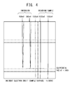
- FIG. 4 shows the orbit of the incident electron when the sample surface is evenly charged at potential of -1,000V. It is seen from the drawing that at the potential being 1,000eV or more, the incident electron reaches the sample while at the potential being less than 1,000eV, the incident electron is inverted before reaching the sample. At the potential being 1,000eV, the energy of the incident electron becomes zero on the sample surface.
- a potential saddle point is formed above the sample charged in a spot-like manner.
- the potential saddle point is an extreme value of a saddle shaped space potential distribution occurring from the charge distribution of the sample.
- FIG. 5B shows the surface potential of the sample in a horizontal direction in FIG. 4A .
- the space potential above the sample is formed as shown in FIG. 5A .
- the space potential distribution of the sample in the horizontal direction (along the cross section X) takes the minimal value at a point Sdl as shown in FIG. 5C .
- the space potential distribution thereof in the vertical direction (along the cross section Z) takes a maximal value at the point Sdl.
- the point Sdl is defined as the potential saddle point.
- the velocity of the incident electron reaching the sample surface cannot become zero even with a change in the accelerated voltage of the electron beam irradiating the sample.
- the potential distribution being several ten voltages or more, it is not able to measure the potential because of the potential saddle point by simply determining whether or not the incident charged particle has reached the sample.
- the surface charge distribution measuring method calculates an estimated surface potential of the sample by charging the sample in a spot-like manner, generating the potential saddle point, and comparing the measured value of the potential at the potential saddle point and the value of the potential at the potential saddle point calculated from a structure model.
- the estimation of the surface charge distribution according to one embodiment of the present invention will be described in detail.
- FIG. 6 shows a relation between the potential saddle point and the accelerated voltage. Under a condition that
- the potential Vsdl at the potential saddle point can be measured by deciding the accelerated voltage Vacc2 as a branching point for reaching or not reaching the sample, while the accelerated voltage Vacc is changed from Vacc1 to Vacc3.
- electromagnetic field analysis is conducted using a structure model pre-set and stored and a tentative charge distribution Q(x, y) to calculate the space potential Vsd1_s at the potential saddle point.
- the electromagnetic field analysis is to analyze the interaction of a subj ect and electric and magnetic fields based on Maxwell's equations using the structure model of the conductor 60 and the sample 23 as a dielectric.
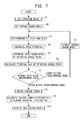
- FIG. 2 shows the structure of the data processor 80 of the surface charge distribution measuring device 1 according to a first embodiment and FIG. 7 is a flowchart for calculating the surface charge using the structure model.
- FIG. 7 is a flowchart for calculating the surface charge using the structure model.
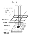
- step S1 the structure model setting portion 801 selects a structure model with the same or similar structure as that of the sample from multiple structure models stored in a not-shown memory unit of the surface charge distribution measuring device 1 and set (sees FIG. 8-9 ) it to be used for the distribution measurement.
- the structure model setting portion 801 is operated automatically or manually by an operator.
- step S2 a surface charge model is set for the set structure model in step S1 by the charge and potential setting portion 802.
- Multiple surface charge models associated with the structure models are also stored in the above memory unit, and one model is selected as a tentative surface charge model.
- the charge and potential setting portion 802 is also operated automatically or manually by an operator.
- step S3 the electromagnetic field analysis is conducted using the selected structure model and tentative surface charge model by the electromagnetic field analysis portion 803.
- step S4 the space potential formed over the sample 23 is calculated by the electromagnetic field analysis portion 803.
- step S5 a space coordinate of the potential saddle point of the sample is specified based on the calculated space potential in step S4 by the electromagnetic field analysis portion 803.
- step S6 the potential Vsd1_s at the potential saddle point is calculated by the characteristic amount calculator 804.
- step S7 the potential Vsdl actually measured and the potential Vsd1_s calculated are compared by the comparator 805.
- a tentative charge distribution Q(x, y) is estimated to be the space charge distribution of the sample 23 by the charge density determining portion 807 in step S8. Then, the flow proceeds to step S9.
- step S9 the surface charge distribution Vs (x, y) of the sample 23 is calculated based on the estimated space charge distribution Q(x, y) by the charge distribution calculator 808.
- step S10 a result of the calculation is displayed on a not-shown display or else of the surface charge distribution measuring device. The flow is completed.
- step S7 when the error is beyond the predetermined range in step S7, the tentative charge distribution Q(x, y) is corrected in step S11 by invoking another charge distribution pre-stored in the memory unit. After the correction, the flow returns to step S3.
- the surface charge distribution measuring method and device can measure the surface charge distribution of the sample with high resolution in the order of micron. Further, it is able to greatly reduce the number of times at which charges and potentials of the sample are measured to only the number of times needed for finding the potential saddle point as well as to greatly reduce the required amount of calculation for the electromagnetic field analysis by calculating the surface charge distribution using the pre-set structure model. Thus, it is able to find the surface charge distribution of the sample in a short period of time.
- Surface charge distribution measuring method and device additionally include a series of steps or elements to correct the charge distribution based on a plurality of measured values other than the potential at the potential saddle point. Thereby, it is able to more accurately find the surface charge distribution.
- the calculated surface charge distribution of the sample is evaluated using an evaluation function expressed by parameters indicating different shapes of the charge density distribution and corrected to one with an optimal value and a shape by comparing the result of the evaluation and the measured value.
- ⁇ 1
- the function is a Gaussian function and the closer to infinity ⁇ is, the closer to a rectangular function the function is.
- the function for representing the surface charge distribution is not limited to the above function.
- mathematizing the surface charge distribution of the sample makes it possible to set an evaluation function such that an error between the measured and calculated surface charge distributions becomes minimal, and makes it easier to search for the condition that the error becomes minimal.
- the evaluation function ⁇ eval which is the surface charge distribution mathematized by the parameters is set on the basis of the above function representing the charge distribution of the sample.
- the evaluation function ⁇ is to extract a characteristic amount as a proper evaluation item from a plurality of physical quantities obtained by the electromagnetic analysis, find a difference between the characteristic amount and a measured characteristic amount and multiple the difference by weight to find the sum of squares.
- the evaluation function can be set to be a minimal or allowable value to determine parameters for the surface charge distribution.
- n is at least 2 or more.
- the characteristic amount used in the evaluation function can be charge potential corresponding to the peripheral charge Qmax, potential at the potential saddle point related to the depth of charge, diameter of a latent image related to the charge dispersion, or size of a latent image. However, it should not be limited to these.
- This evaluation function uses two characteristic amounts, the charge depth QD and charge dispersion ⁇ , by way of example.
- step S21 the charge depth QD and charge dispersion ⁇ as characteristic amounts are arranged at two orthogonal axes as shown in FIG. 11 and 5 points (5 ⁇ 5 in the drawing) around the initial values of the two characteristic amounts are selected to find the evaluation function ⁇ eval for the selected combinations.
- step S22 the best evaluated point ⁇ eval_best (with best or lowest value ⁇ eval) is found from the calculated 25 points (5 ⁇ 5).
- step S23 a determination is made on whether or not the value at ⁇ eval_best reaches a predetermined target value. The flow proceeds to step S24 when the value has not reached the target value. The calculation is completed when the value has reached the target value.
- step S24 a determination is made on whether or not the point ⁇ eval_best is included in about the center, that is, the center 3 ⁇ 3 area of the search area as shown in FIG. 11A .
- the flow proceeds to step S26 when the value is not included in the center area.
- step S26 with the values of ⁇ QD and ⁇ fixed, the 5 ⁇ 5 search area is moved so that the best evaluated point comes at the center of the search area as shown in FIG. 11B . Then, returning to step S21, the ⁇ eval is calculated and evaluated for the new 5 ⁇ 5 search area. These steps are repeated to roughly specify the search area.
- FIGs. 11A, 11B An example of the step S26 is shown in FIGs. 11A, 11B .
- the ⁇ eval is calculated again in an area around the best evaluated point.
- step S24 when the point ⁇ eval_best is around the center of the evaluated 5 ⁇ 5 search area as shown in FIG. 12A , with the point as the center of the area, the values of ⁇ QD and ⁇ are set to a half, that is, ⁇ QD ⁇ QD/2, ⁇ /2, as shown in FIG. 12B .
- the search area is narrowed from the one used for the first evaluation, and the flow returns to step S21 so that 5 ⁇ 5 area is searched again to find a point with a best evaluated value. This is repeated to make the charge depth QD and charge dispersion ⁇ closer to the optimal combination until the value at the point ⁇ eval_best reaches the target value in step S23. Thus, it is made possible to automatically search for the optimal parameters.
- ⁇ and ⁇ QD can be set to arbitrary values. It is preferable that the initial values are set to ones 8 to 32 times larger than the target values for the purpose of searching a broader area. With the final target value being 1 ⁇ m and potential being 2V, the proper value of ⁇ is about 8 to 32 ⁇ m and that of ⁇ QD is about 16 to 64V. Further, the number of the parameters used for the evaluation function can be 3 or more.
- the calculated surface charge distribution of the sample is corrected by the electromagnetic field analysis based on the two characteristic amounts.
- the surface charge distribution measuring method it is able to more accurately obtain the surface charge distribution of the sample since the calculated surface charge distribution is corrected according to multiple measured values other than the potential at the potential saddle point.
- the surface charge distribution measuring method can be configured that for measuring the potential saddle point, the applied voltage Vsub to the conductor 60 as a backside electrode can be changed while the accelerated voltage Vacc is fixed. In this manner the incident optical system can be fixed whereas the focal length or else of the incident optical system is changed by a change in the accelerated voltage.
- the accelerated voltage is higher than the potential saddle point so that an incident charged particle can exceed the potential saddle point and reaches the sample and causes a secondary electron.
- the energy of the secondary electron is, however, too small to escape from the potential saddle point. As a result, the secondary electron cannot reach the detector.
- the applied voltage being Vsub2
- Vsub2 it becomes a branching point for detection or non-detection of a signal and the potential of potential saddle point and the accelerated voltage can be considered to match each other.
- the potential Vsd1_s of the measured potential saddle point can be measured.
- FIG. 15 is a flowchart for calculating the surface charge using the structure model.
- the surface charge distribution measuring method according to the present embodiment is described referring to the flowchart.
- the structure model setting portion 801 selects a structure model with the same or similar structure as that of the sample from multiple structure models stored in the not-shown memory unit of the surface charge distribution measuring device 1 and sets (sees FIG. 8-9 ) it to be used for the distribution measurement.
- the structure model setting portion 801 is operated automatically or manually by an operator.
- step S32 a surface charge model is set for the set structure model in step S31 by the charge and potential setting portion 802.
- Multiple surface charge models associated with the structure models are also stored in the above memory unit, and one model is selected as a tentative surface charge model.
- the charge and potential setting portion 802 is also operated automatically or manually by an operator.
- step S33 an applied voltage to the conductor 60 is set to the voltage Vsub2 which is decided to be the branching point for the incident charged particle to reach or not reach the sample while the applied voltage is changed from Vsub1 to Vsub3 as described above.
- step S34 the electromagnetic field analysis is conducted using the selected structure model and tentative surface charge by the electromagnetic field analysis portion 803.
- step S35 the space potential formed over the sample 23 is calculated as a part of the electromagnetic field analysis by the electromagnetic field analysis portion 803.
- step S36 the space coordinate of the potential saddle point of the sample is determined on the basis of the calculated space potential in step S35 by the electromagnetic field analysis portion 803.
- step S37 the potential Vsd1_s at the potential saddle point is calculated by the characteristic amount calculator 804.
- step S38 the potential Vsdl measured and the potential Vsd1_s calculated are compared by the comparator 805.
- the tentative charge distribution model Q(x, y) is estimated to be the space charge distribution of the sample 23 by the charge density determining portion 807 in step S39. Then, the flow proceeds to step S40.
- step S40 the surface charge distribution Vs (x, y) of the sample 23 is calculated on the basis of the estimated space charge distribution by the charge distribution calculator 808.
- step S41 a result of the calculation is displayed on a not-shown display or else of the surface charge distribution measuring device. The flow is completed.
- step S38 when the error is outside the predetermined range in step S38, the tentative charge distribution model Q(x, y) is corrected in step S42 by invoking another charge distribution pre-stored in the memory unit. After the correction, the flow returns to step S34.
- the surface charge distribution measuring method and device can also measure the surface charge distribution of the sample with high resolution in the order of micron. Further, it is able to greatly reduce the number of times at which charges and potentials of the sample are measured to only the number of times needed for finding the potential saddle point as well as to greatly reduce the required amount of calculation for the electromagnetic field analysis by calculating the surface charge distribution using the pre-set structure model. Thus, it is able to find the surface charge distribution of the sample in a short period of time.
- the surface charge distribution is calculated using the charge dispersion as a characteristic amount other than the potential at the potential saddle point.
- the estimate or target value of the charge dispersion can be set in accordance with an electron beam size irradiated to the photoreceptor, exposure amount, or lighting time.
- the electromagnetic field analysis is conducted (in step S3 in FIG. 7 ) using the set surface charge model (in step S2 in FIG. 7 ) to calculate the electric field intensity distribution on the sample surface.
- the coordinate can be approximately calculated by straight-line approximation of two points (points A, B in FIG. 16 ) immediately before and after the positive to negative inversion of the vertical electric field intensity and by bisection as shown in FIG. 16 . In the following calculation of the graph in FIG. 16 is described.
- the sample 23 is scanned with the electron beam and secondary electron emitted is detected by the detector 24 (scintillator).
- the emitted electron is converted into an electric signal to generate a contrast image for observation.
- the contrast image is generated since the amount of the secondary electron detected from a non-exposed portion with remnant charge is larger than that from an exposed portion.
- a dark portion can be considered as a latent image.
- FIG. 17A shows the potential distribution in the space between the detector 24 and the sample 23 with a contour.
- the sample surface except for a potential attenuated portion by optical attenuation is evenly charged with negativity. Since the detector 24 is given positive potential, the closer to the detector 24 from the sample surface a position is, the higher the potential of the position is, as shown in the solid contour.
- FIG. 17A the potential contours near the point Q3 as the center of the negative potential attenuated portion are semielliptical.
- the potential distribution of the portion is such that the closer to the point Q3, the higher the potential. Therefore, electric power acts on a secondary electron el3 occurring about the point Q3 to pull it toward the sample 23 as indicated by the arrow G3, so that the secondary electron el3 is captured by a potential hole indicated by a broken contour and prevented from moving to the detector 24.
- FIG. 17B is a graph showing the potential hole.
- a part with a larger intensity corresponds to the evenly negative-charged portion of the latent image (the points Q1, Q2 in FIG. 17A ) while a part with a lower intensity corresponds to the optically irradiated portion or an image portion of the latent image (the point Q3 in FIG. 17A ).
- the surface potential distribution V(X, Y) can be determined for each small area associated with the sampled signal, using sampling time as a parameter. This makes it possible to represent the surface potential distribution V(X, Y) or potential contrast image as two-dimensional image data. With use of an output device, the pattern of an electric latent image can be provided as a visual image.
- the intensity of the secondary electron is represented by a contrast of brightness
- an image portion of an electric latent image is dark while the other portion is bright so that a contrast image in line with the surface charge distribution can be obtained.
- the surface charge distribution can be found from a known surface potential distribution.
- an apparent charge density on the interfaces of the conductor and dielectric is found as a direct solution.
- a known electrode potential is converted to an apparent charge density using, as a boundary condition, an unknown charge density on the sample and geometric arrangement in the form of algebraic equation of the structure models of the conductor and dielectric in a space to be analyzed.
- the space field is directly decided from the apparent charge density, and the charge density on the sample is decided by comparing calculated electron orbit simulation data with data on the measured detection signal.
- the apparent charge density refers to a tentative value of charge density on the sample interface which forms an electromagnetic field equivalent to the electrode potential applied to the conductor.
- a coefficient matrix is obtained from the geometric arrangement in the form of algebraic equation of the conductor and dielectric in a space to be analyzed, to solve simultaneous linear equations with n-unknowns using the coefficient matrix, the field potential, the potential of the conductor and the charge density on the interface of the dielectric as a boundary condition. Details are described in the following.
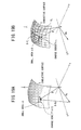
- FIG. 18 shows a measuring device for detecting signals.
- the conductor 60, an insulator plate 61 and a ground substrate (GND) 62 are layered to form a mount for the sample.
- the sample 23 as a photoreceptor is placed on the conductor 60 applied with the voltage Vsub.
- An electron beam 104 is irradiated to the photoreceptor 23 from above.
- the objective lens 20 is disposed on the path of the electron beam 104 so as to adjust the electron beam 104 to have a properly shaped traverse section to irradiate the photoreceptor 23.
- a grid mesh 106 is provided above the photoreceptor 23.
- the detector 24 is provided obliquely above the grid mesh 106 to detect electrons of the electron beam 104 reflected by the photoreceptor 23.
- the shape and film thickness of the sample or photoreceptor, shape of electrode on the back face of the sample, and the conductor and dielectric near the sample are large influential factors to the electron orbit. Therefore, these elements are geometrically arranged with the position of the detector, the structure of the electron beam optical system, and the property of the respective optical elements of the optical system taken into consideration when necessary. Then, the permittivity of the dielectric and the applied voltage to the conductor are set. The electrode potential on the back face of the sample used for the measurement is set. The elements disposed away from the sample do not affect the electron orbit much so that they can be omitted or simplified.
- the initial charge density distribution is set on the sample surface. It can be arbitrarily set since it is changed according to a result of comparison with measured data. However, preferably, it is set to about an expected value. The closer to the measured value it is, the shorter the optical convergence time becomes.
- a boundary area is divided into small areas ⁇ Si as shown in FIG. 19B .
- the charge density in the small areas is approximately set to ⁇ i which is constant.
- a relation between a known electrode potential and the apparent charge density is expressed by a determinant shown in FIG. 20A .
- ⁇ 1 to ⁇ m are known potentials on the conductor face and ⁇ r is surface charge density to be measured and values are input before the comparison.
- ⁇ in the right-hand side is apparent charge density and ⁇ 1 to ⁇ m are apparent charge densities on the conductor face.
- the coefficient matrix Fji as elements of coefficient determinant is determined by equations shown in FIGs. 20A, 20B from the geometrical arrangement of the conductor and dielectric in the space to be analyzed.
- Rj is coordinate (xj, yj, zj)
- ⁇ is a sampling point at Rj on the conductor or dielectric surface
- ji is Kronecker delta
- nj is normal vector of an element j
- ⁇ 0 vacuum permittivity
- ⁇ 1 permittivity outside the dielectric interface
- ⁇ 2 is permittivity inside the dielectric interface.
- the apparent charge density can be found by determining the coefficient matrix Fji and solving the determinant by simultaneous linear equations or inverse matrix calculation using the coefficient matrix, the potential of the conductor and the charge density on the dielectric interface for the boundary condition.
- the known electrode potentials ⁇ 1 to ⁇ m and the surface charges ( ⁇ r) m+1 to ( ⁇ r)n can be converted to apparent charge densities ⁇ 1 to ⁇ m and ⁇ m+1 to ⁇ n, respectively, as shown in FIG. 21A .
- the structure model can be represented by one or a combination of a part or all of six basic model faces of flat, cylindrical, disc, conical, spherical, and torus shown in FIGs. 22A to 22F , respectively.
- the basic model faces, the five rotationally symmetrical faces and the flat face represented in the two-dimensional space are expressed by a function of a local coordinate system associated with the basic models.
- the integrand thereof can be a relatively simple equation.
- double integration Fji is directly calculated by numerical integration.
- a first integration can be analytically done.
- the coefficient matrix Aji for the flat face can be expressed in the form including log by the following equations (6) to (9).
- Aji 1 4 ⁇ ⁇ 0 ⁇ ⁇ - ⁇ yi 2 ⁇ yi 2 log ⁇ 1 + ⁇ ⁇ x i + P x i - ⁇ ⁇ x i 2 - x j + C + x i - ⁇ ⁇ x i 2 - x j 2 ⁇ dy
- C y j - y i + y 2 + z j 2
- the first integration of the double integration is analytically calculated and only the other integration is calculated by numerical integration. Thus, it is able to greatly reduce the amount of calculation time for the coefficient matrix Fji.
- the surface charge distribution measuring method is configured to correct the surface charge distribution on the sample calculated in any of the above embodiments by using a threshold potential Vth (x, y) indicating a state of the charge distribution of the sample, and to find more accurate surface charge distribution.
- Vth a threshold potential
- the preceding steps of calculating the surface charge distribution are the same as in the above embodiments; therefore, a description thereof is omitted.
- the threshold potential Vth is expressed by the following equation: where Vacc is the accelerated voltage of the electron beam and Vsub is a voltage applied to the conductor. Vth (x, y) represents a value of the threshold potential Vth at coordinate (x, y).
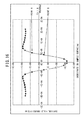
- FIGS. 23A to 23C show results of measurement of the Vth (x, y) by signal detection.
- the accelerated voltage of the electron gun two-dimensionally scanning is set to -1,800V.
- the curve in FIG. 23A indicates the results of detection of the threshold potential distribution caused by the surface charge distribution of the sample.
- the value of the threshold potential Vth negatively increases and it is about -850V in a periphery area beyond a radius 75 ⁇ m from the center.
- the ellipse shown in FIG. 23B is an imaged output of the detector when the voltage Vsub of the back face of the sample is set to -1,150V.
- the threshold potential Vth is -650V (Vacc - Vsub).
- the ellipse in the FIG. 23C is the same when the voltage Vsub is set to -1,100V.
- the threshold potential Vth is -700V.
- the dark and light portions represent a difference in the intensity of the detection signal.
- the amount of detection signal in the light portion is larger than that in the dark portion. That is, the light portion is an area in which the incident electron is inverted before reaching the sample while the dark portion is an area in which the incident electron has reached the sample.
- the boundary between the light and dark portions indicates that the landing energy is almost zero there.
- a value of the boundary between the light and dark portions is defined to be the value of the threshold potential Vth.
- the sample surface is repetitively scanned with the electron beam while the accelerated voltage Vacc or applied voltage Vsub is changed, to measure the threshold potential Vth (x, y) in micron scale.
- FIG. 25 is a flowchart for measuring the threshold potential Vth (x, y) by the signal detection.
- the threshold potential Vth is set, and in step S52 a contrast image is captured.
- the contrast image is binarized and in step S54 the latent image diameter is calculated.
- the steps 51 to 54 are then repeated at a predetermined number of times (steps S55, S57) to calculate the threshold potential Vth (x, y) in step S56.
- the structure model in FIGs. 8 , 9 and an unknown surface charge are set to calculate the orbit of the primary charged particle.
- the applied voltage to the back face of the sample is Vsub.
- the electron is used for the primary charged particle. It is set to be vertically incident on the sample from a distance z0 away from the sample surface. It is preferable to set the distance z0 to be further than that from the upper grid to the sample.
- the incident electron is given the initial coordinate and the accelerated voltage Vacc ( ⁇ 0) or the initial velocity equivalent to the accelerated voltage Vacc.
- the detector Although whether or not the orbit of the incident electron has reached the detector can be analyzed, it increases a length of time for the calculation. The accuracy of the analysis by determining whether the incident electron has reached the sample is sufficiently high.
- FIG. 24A shows a relation between surface potential calculated in X-axis direction and scan position by way of example, to compare Vth_s (x, y) and Vth_m (x, y) and find if they are equal to each other. They can be compared by calculating a difference ⁇ (x, y) between them.
- FIG. 24B shows the measured surface potential and the calculated surface potential overlapping with each other by way of example.
- a minimal Vth_m (x, y) can be selected by finding the differences among all the Vth_m (x, y).
- the evaluation value M can be a squared sum of the differences obtained by the following equation:
- the charge distribution model is corrected in accordance with the value of the ⁇ (x, y). For example, if the difference ⁇ (x, y) includes a bias component, the average potential is determined to be different so that the bias component is added to each potential of the charge distribution model.
- the shape of surface charge distribution for example, depth and width is determined to be different so that the shape of the charge distribution model is corrected to be the uneven shape. Thereby, a more appropriate charge distribution model is obtainable.
- the surface charge is determined by calculating the electron orbit and comparing it with the measured result.
- a static electric field is decided from a known charge distribution.
- physical quantities such as potential distribution V(x, y), electric field intensity can be measured.
- FIG. 26 shows distribution data on the threshold potential Vth and data on the surface charge distribution Vs calculated from the final charge density distribution on the dielectric surface. Between them there are an error of 2V or less in potential depth and an error of 1 ⁇ m or less in charge dispersion. Further, it is seen from FIG. 26 that the Vth distribution Vth (x, y) is inside the surface charge distribution Vs (x, y). That is, a relation, Vs (x, y) - Vth (x, y) ⁇ 0 is satisfied. Thus, the surface charge distribution corrected according to the value of threshold potential Vth (x, y) measured or calculated is highly accurate.
- the surface charge distribution measuring method is configured to correct the surface charge distribution calculated in any of the above embodiments by electron orbit analysis, to find more accurate surface charge distribution.
- the electron orbit can be calculated on the basis of electric field at an arbitrary point in a space which can be found by surface integral of the conductor and sample interface using the apparent charge density described in the fifth embodiment. That is, the surface charge distribution can be corrected by the electron orbit analysis on the basis of the apparent charge density.
- the measured value of the detection signal obtained by the detector 24 when the electron beam is actually irradiated and a calculated value thereof by the electron orbit analysis are compared.
- the calculated surface charge distribution is estimated to be the actual charge distribution when the measured value and the calculated value coincide with each other or a difference therebetween is within an allowable range.
- the apparent charge density is calculated again to correct the surface charge distribution.
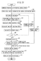
- This series of processes which are shown in FIG. 27 are repeated until the difference falls within the allowable range.
- the surface charge distribution measuring method according to the present embodiment is described in detail. Note that before the first step S61 in FIG. 27 , the steps S1 to S6 and S11 in FIG. 7 are performed but omitted therefrom.
- the flowchart starts at step S61 equivalent to step S7 in FIG. 7 .
- step S61 a measured potential Vsdl and a calculated potential Vsd1_s at the potential saddle point are compared (step S7 in FIG. 7 ).
- step S62 the parameters for the shape of charge distribution such as shape, film thickness of the sample as a photoreceptor, and shape of electrode on the back face of the sample are tentatively decided and substituted into the coefficient matrix in FIG. 20 (see fifth embodiment).
- step S63 the applied voltage Vsub is set and applied to the conductor 60 on which the sample is placed (see fifth embodiment).
- step S64 a known electrode potential is converted into the apparent charge density using, as a boundary condition, an unknown charge density on the sample and the geometric arrangement in the form of algebraic equation of the structure models of the conductor and dielectric in a space to be analyzed (see fifth embodiment).
- step S65 the space field is calculated using the apparent charge density (see fifth embodiment).
- step S66 the orbit of an incident electron on the sample is analyzed according to the apparent charge density (see fifth embodiment).
- step S67 a value of the branching point for allowing the electron to reach or not to reach the sample is found using the result of the electron orbit analysis (see sixth embodiment). Specifically, a primary charged particle is incident on the sample at the accelerated voltage Vacc ( ⁇ 0) from the initial coordinate with a distance z0 away from the sample surface. This simulation is such that the voltage Vsub is applied to the back face of the sample, and a determination is made on whether the orbit of the primary charged particle reaches or is inverted before reaching the sample to decide the initial coordinate (x0, y0, z0).
- step S68 a determination is made on whether or not the number of times i at which the steps S63 to S69 are repeated is a predetermined number N.
- the simulation is repeated at a required number of times while the values of Vsub and Vacc equivalent to later-described measured values are changed when necessary.
- the repetition number i is not the predetermined number N
- the flow proceeds to step S74 to change the applied voltage Vsub and returns to step S63.
- the repetition number i is the predetermined number N
- the flow proceeds to step S69.
- a value Vth_m (x, y) is also measured aside from the value Vth_s (x, y) calculated in step S69 as in the sixth embodiment.
- the calculated value Vth_s (x, y) and measured value Vth_m (x, y) are compared to find if they match each other in step S70, as in the sixth embodiment. When they do not match each other, the surface charge distribution model is corrected in step S75 and the series of steps from S63 is performed again. When they match, the flow proceeds to step S71.
- step S71 the tentatively decided parameters in step S62 are determined to be correct, and the shape of the surface charge is decided according to the parameters.
- step S72 the surface charge distribution is calculated according to the decided shape of surface charge. Also, a static electric field is decided from the charge distribution. By analyzing the static electric field by Poisson equation or else, physical quantities such as potential distribution, electric field intensity distribution can be also measured.
- step S73 the result of the calculation is displayed on a not-shown display of the surface charge distribution measuring device, completing the entire flow.
- FIG. 28 shows another example of a surface charge distribution measuring device with a function to generate a latent image.
- An electrophotographic photoreceptor is used for the sample 23.
- An organic photoreceptor includes a charge generating layer (CGL) and a charge transport layer (CTL) superimposed on a conductive support element.
- CTL charge transport layer
- a charge generating material (CGM) of the charge generating layer absorbs light and generates both positive and negative charge carriers.
- One of the carriers is injected by electric field into the charge transport layer and the other is into the conductive support element.
- the carrier in the charge transport layer moves to the surface by electric field, and is coupled with the charge on the photoreceptor surface and disappears. Thereby, a charge distribution or an electric latent image is formed on the photoreceptor surface.
- a surface charge distribution measuring device 10 is comprised of a pattern forming unit 220 in addition to the surface charge distribution measuring device 1 in any of the above embodiments.
- FIG. 28 omits to show a control system.
- the pattern forming unit 220 comprises a semiconductor laser 201 with a wavelength of 400 nm to 1,000 nm to which the photoreceptor is sensitive, a collimate lens 203, an aperture 205, and three imaging lenses 207, 209, 211. Also, an LED 213 is placed in the vicinity of the sample 23 to electrically neutralize the sample surface.
- the pattern forming unit 220 and the LED 213 are controlled by a not-shown control system.
- Latent image generation of the surface charge distribution measuring device 10 is simply described.
- the surface of the photoreceptor is evenly charged.
- the accelerated voltage is set to a higher voltage than one at which a secondary electron emission ratio becomes 1 so that the amount of incident electron exceeds the amount of emitted electron. Because of this, the electron is accumulated on the sample and charge up occurs thereon. As a result, the sample is negatively charged.
- the sample can be charged with a desirable potential by controlling the accelerated voltage and light irradiation time.
- the electron beam is irradiated from the electron gun 11 to the sample 23.
- charge up occurs on the sample as shown in FIG. 29A so that the sample can be evenly, negatively charged.
- FIG. 29B There is a relation between the accelerated voltage and saturated charge potential shown in FIG. 29B .
- the larger the level of probe current the shorter the length of time in which a target charge potential is acquired.
- the probe current of 1nA or more is preferable.
- the amount of incident electron is reduced to 1/100 to 1/1,000 and the semiconductor laser 201 of the pattern forming unit 220 emits laser beam.
- the laser beam from the semiconductor laser 201 is converted by the collimate lens 203 to approximate parallel light and adjusted by the aperture 205 to be of a predetermined beam size. Then, it is focused on the sample surface through the imaging lenses 207, 209, 211. Thus, a pattern of the latent image is formed on the sample surface.
- the surface charge distribution device 10 in FIG. 28 includes a vacuum chamber 30 in which the sample is charged and exposed. Therefore, it can start data acquirement immediately after the latent image generation and complete it within 10 seconds even when the applied voltage required for obtaining a latent image profile is changed at multiple times. By changing the applied voltage as above, it is possible to acquire latent image profile information.
- An upper electrode can be additionally provided above the sample when needed. With the upper electrode, the influence of the space field occurring from the charge distribution of the sample can be localized in an area up to the upper electrode so that the structure model can be more simplified.
- the above embodiments have described an example in which the sample is a plate-like element.
- the sample can be a cylindrical photoreceptor, for example.
- Such a cylindrical photoreceptor is applicable to a photoreceptor drum used in an electrophotographic imaging device such as a laser printer, a digital copier. Accordingly, by feeding back the measurement results of the surface charge distribution for designing of the device, it is made possible to improve the quality of each process of the image generation and realize an imaging device which excels in durability and energy saving and can stably generate high-quality images.
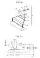
- an exposure unit 76 shown in FIG. 30 comprises an optical scan unit including a semiconductor laser 110, a collimate lens 111, an aperture 112, a cylinder lens 113, a reflective mirror 114, a polygon mirror 115, two scan lenses 116, 117, and a reflective mirror 118 by way of example.
- the semiconductor laser 110 emits laser beam for exposure.
- the collimate lens 111 adjusts the laser beam from the semiconductor laser 110 to approximate parallel light.
- the aperture 112 defines the beam size of the beam having transmitted from the collimate lens 111. By changing the size of the aperture 112, an arbitrary beam size of light within the range of 20 ⁇ m to 200 ⁇ m can be generated.
- the cylinder lens 113 adjusts the light from the aperture 112 to travel only in one direction.
- the mirror 114 bends the optical path from the cylinder lens 113 to the polygon mirror 115.
- the polygon mirror 115 comprises a plurality of deflection faces to deflect the light from the mirror 114 at constant angular velocity within a predetermined angular range.
- the two scan lenses 116, 117 convert the light deflected by the polygon mirror 115 to light at constant angular velocity.
- the mirror 118 bends the optical path from the scan lens 117 to a sample 71.
- the operation of the exposure unit 76 is described.
- Light from the semiconductor laser 110 is collected near the deflection faces of the polygon mirror 115 via the collimate lens 111, aperture 112, cylinder lens 113, and reflective mirror 114.
- the polygon mirror 115 is rotated by a not-shown motor at a constant velocity in a direction indicated by the arrow in FIG. 31 .
- the collected light is deflected at a constant angular velocity, and converted through the two scan lenses 116, 117 to scan the mirror in a longitudinal direction at constant angular velocity within a predetermined angular range.
- the light scans the surface of the sample 71. That is, optical spots move in a bus direction of the sample 71 to thereby form an arbitrary latent image pattern including a line pattern.
- the light source can be a multi beam scan optical system such as VCSEL.
- ion beam is usable and by use of the ion beam, an ion gun in replace of the electron gun is used.
- an ion gun in replace of the electron gun is used.
- the accelerated voltage should be positive and the sample is applied with a bias voltage so that the surface potential becomes positive.
- the above embodiments have described an example in which the surface potential of the sample is negative. However, it can be positive i.e., the surface charge can be positive. In this case a positive ion beam such as gallium can be irradiated to the sample.
- the partition 16 is placed on -Z side of the beam blanking electrode 15.
- a thermionic emission electron gun or a schottky emission (SE) electron gun shown in FIG. 31 is also usable.
- the schottky emission electron gun in FIG. 31 comprises an emitter 11, a suppressor electrode 73, an extracting electrode 71, and an acceleration electrode 72.
- Ie is emission current
- Vs is suppressor voltage.
- the SE electron gun is also called as thermally assisted field emission electron gun.
- the above embodiments have described an example where the surface charge distribution is obtained by detecting the primary inverted electron.
- the surface charge distribution can be obtained by detecting the secondary electron when there is no possibility that it is affected by the material or surface shape of a sample, for example.
- the surface charge distribution measuring method and device can reduce the amount and number of times for the analysis based on measured values and measure the surface charge distribution of a sample such as a photoreceptor with high resolution in the order of micron and in a short length of time by deciding a structure model on the basis of a potential at the potential saddle point above the sample and an accelerated voltage of an incident charged particle to calculate the surface charge distribution of the sample according to a tentative space potential distribution associated with the structure model.
Landscapes
- Engineering & Computer Science (AREA)
- Microelectronics & Electronic Packaging (AREA)
- Physics & Mathematics (AREA)
- General Physics & Mathematics (AREA)
- Analysing Materials By The Use Of Radiation (AREA)
- Photoreceptors In Electrophotography (AREA)
- Cleaning In Electrography (AREA)
- Testing Or Measuring Of Semiconductors Or The Like (AREA)
Applications Claiming Priority (1)
| Application Number | Priority Date | Filing Date | Title |
|---|---|---|---|
| JP2010199367A JP5568419B2 (ja) | 2010-09-06 | 2010-09-06 | 表面電荷分布の測定方法および表面電荷分布の測定装置 |
Publications (3)
| Publication Number | Publication Date |
|---|---|
| EP2426559A2 true EP2426559A2 (fr) | 2012-03-07 |
| EP2426559A3 EP2426559A3 (fr) | 2015-01-14 |
| EP2426559B1 EP2426559B1 (fr) | 2017-08-30 |
Family
ID=44719334
Family Applications (1)
| Application Number | Title | Priority Date | Filing Date |
|---|---|---|---|
| EP11180083.5A Not-in-force EP2426559B1 (fr) | 2010-09-06 | 2011-09-05 | Dispositif et procédé de mesure de distribution de charge de surface |
Country Status (3)
| Country | Link |
|---|---|
| US (1) | US8847158B2 (fr) |
| EP (1) | EP2426559B1 (fr) |
| JP (1) | JP5568419B2 (fr) |
Cited By (2)
| Publication number | Priority date | Publication date | Assignee | Title |
|---|---|---|---|---|
| CN111722026A (zh) * | 2020-05-29 | 2020-09-29 | 清华大学 | 基于磁声系统的绝缘介质空间电荷测量方法及系统 |
| CN114034943A (zh) * | 2021-11-09 | 2022-02-11 | 华北电力大学 | 表面电位衰减测量装置、方法及电荷输运过程确定方法 |
Families Citing this family (15)
| Publication number | Priority date | Publication date | Assignee | Title |
|---|---|---|---|---|
| JP5884523B2 (ja) | 2012-02-02 | 2016-03-15 | 株式会社リコー | 潜像電荷総量の測定方法、潜像電荷総量の測定装置、画像形成方法及び画像形成装置 |
| JP6115191B2 (ja) | 2013-03-07 | 2017-04-19 | 株式会社リコー | 静電潜像形成方法、静電潜像形成装置及び画像形成装置 |
| JP5617947B2 (ja) * | 2013-03-18 | 2014-11-05 | 大日本印刷株式会社 | 荷電粒子線照射位置の補正プログラム、荷電粒子線照射位置の補正量演算装置、荷電粒子線照射システム、荷電粒子線照射位置の補正方法 |
| JP6322922B2 (ja) | 2013-08-08 | 2018-05-16 | 株式会社リコー | 画像形成方法、画像形成装置 |
| JP6418479B2 (ja) | 2013-12-25 | 2018-11-07 | 株式会社リコー | 画像形成方法、画像形成装置 |
| US9513573B2 (en) | 2014-09-04 | 2016-12-06 | Ricoh Company, Ltd. | Image forming method, image forming apparatus, and printed matter production method |
| US9981293B2 (en) | 2016-04-21 | 2018-05-29 | Mapper Lithography Ip B.V. | Method and system for the removal and/or avoidance of contamination in charged particle beam systems |
| CN109344431B (zh) * | 2018-08-24 | 2023-04-14 | 国网安徽省电力有限公司建设分公司 | 基于模拟电荷法精确计算导线表面电场强度的方法 |
| CN110738009B (zh) * | 2019-10-14 | 2023-08-04 | 山东科技大学 | 一种输电线路电场计算中导线内模拟电荷的设置方法 |
| CN113009242B (zh) * | 2021-02-25 | 2022-10-04 | 西安理工大学 | 一种阵列式磁通门表面电势分布及衰减的测量装置及方法 |
| CN113671275B (zh) * | 2021-07-09 | 2023-06-06 | 深圳供电局有限公司 | 多层油纸绝缘空间电荷预测方法及设备 |
| CN114371379B (zh) * | 2021-12-20 | 2024-11-26 | 同济大学 | 一种空间电荷注入阈值电场的测量方法及系统 |
| CN115640731A (zh) * | 2022-11-11 | 2023-01-24 | 电子科技大学长三角研究院(湖州) | 同步轨道航天器介质内带电风险评估方法、系统及终端 |
| CN117074801B (zh) * | 2023-10-14 | 2024-02-13 | 之江实验室 | 一种悬浮带电微球测量电场的装置及方法 |
| CN119180148B (zh) * | 2024-09-23 | 2025-12-16 | 武汉大学 | 一种旋转风机叶片表面多荷电状态耦合的分析方法及装置 |
Citations (10)
| Publication number | Priority date | Publication date | Assignee | Title |
|---|---|---|---|---|
| JPS59842A (ja) | 1982-06-28 | 1984-01-06 | Fujitsu Ltd | 電子ビ−ム装置 |
| JPH0320010A (ja) | 1989-06-16 | 1991-01-29 | Matsushita Electron Corp | 電子ビーム露光装置 |
| JPH0349143A (ja) | 1989-07-18 | 1991-03-01 | Fujitsu Ltd | 電子ビームによる静電潜像の画像取得方法 |
| JPH03261057A (ja) | 1990-03-08 | 1991-11-20 | Jeol Ltd | 荷電粒子ビーム装置 |
| JPH10334844A (ja) | 1997-06-03 | 1998-12-18 | Jeol Ltd | 走査電子顕微鏡 |
| JP2003295696A (ja) | 2002-04-05 | 2003-10-15 | Ricoh Co Ltd | 静電潜像形成方法および装置、静電潜像の測定方法および測定装置 |
| JP2004251800A (ja) | 2003-02-21 | 2004-09-09 | Ricoh Co Ltd | 表面電荷分布測定方法および装置 |
| JP2005166542A (ja) | 2003-12-04 | 2005-06-23 | Ricoh Co Ltd | 表面電位分布の測定方法および表面電位分布測定装置 |
| JP2006344436A (ja) | 2005-06-08 | 2006-12-21 | Ricoh Co Ltd | 表面電位分布測定方法及び表面電位分布測定装置 |
| JP2008076100A (ja) | 2006-09-19 | 2008-04-03 | Ricoh Co Ltd | 表面電荷分布あるいは表面電位分布の測定方法、及び測定装置、並びに画像形成装置 |
Family Cites Families (21)
| Publication number | Priority date | Publication date | Assignee | Title |
|---|---|---|---|---|
| JPH07102744B2 (ja) | 1986-08-06 | 1995-11-08 | 株式会社リコー | 可逆性感熱記録材料 |
| JPH03200100A (ja) | 1989-12-28 | 1991-09-02 | Toretsuku Japan Kk | X線顕微鏡 |
| US5834766A (en) | 1996-07-29 | 1998-11-10 | Ricoh Company, Ltd. | Multi-beam scanning apparatus and multi-beam detection method for the same |
| US6081386A (en) | 1997-04-15 | 2000-06-27 | Ricoh Company, Ltd. | Optical scanning lens, optical scanning and imaging system and optical scanning apparatus incorporating same |
| US6376837B1 (en) | 1999-02-18 | 2002-04-23 | Ricoh Company, Ltd. | Optical scanning apparatus and image forming apparatus having defective light source detection |
| JP3503929B2 (ja) | 1999-06-09 | 2004-03-08 | 株式会社リコー | 光走査用レンズおよび光走査装置および画像形成装置 |
| JP2001091875A (ja) | 1999-09-22 | 2001-04-06 | Ricoh Co Ltd | 光走査装置 |
| JP2001343604A (ja) | 2000-05-31 | 2001-12-14 | Ricoh Co Ltd | 光走査用レンズ・光走査装置および画像形成装置 |
| US6999208B2 (en) | 2000-09-22 | 2006-02-14 | Ricoh Company, Ltd. | Optical scanner, optical scanning method, scanning image forming optical system, optical scanning lens and image forming apparatus |
| JP4139209B2 (ja) | 2002-12-16 | 2008-08-27 | 株式会社リコー | 光走査装置 |
| JP4095510B2 (ja) * | 2003-08-12 | 2008-06-04 | 株式会社日立ハイテクノロジーズ | 表面電位測定方法及び試料観察方法 |
| US7239148B2 (en) | 2003-12-04 | 2007-07-03 | Ricoh Company, Ltd. | Method and device for measuring surface potential distribution |
| US7403316B2 (en) | 2004-01-14 | 2008-07-22 | Ricoh Company, Ltd. | Optical scanning device, image forming apparatus and liquid crystal device driving method |
| US7612570B2 (en) | 2006-08-30 | 2009-11-03 | Ricoh Company, Limited | Surface-potential distribution measuring apparatus, image carrier, and image forming apparatus |
| US8314627B2 (en) | 2006-10-13 | 2012-11-20 | Ricoh Company, Limited | Latent-image measuring device and latent-image carrier |
| JP5176328B2 (ja) * | 2007-01-15 | 2013-04-03 | 株式会社リコー | 静電特性計測方法及び静電特性計測装置 |
| JP5103644B2 (ja) | 2007-08-24 | 2012-12-19 | 株式会社リコー | 光走査装置及び潜像形成装置及び画像形成装置 |
| US8143603B2 (en) | 2008-02-28 | 2012-03-27 | Ricoh Company, Ltd. | Electrostatic latent image measuring device |
| JP5262322B2 (ja) | 2008-06-10 | 2013-08-14 | 株式会社リコー | 静電潜像評価装置、静電潜像評価方法、電子写真感光体および画像形成装置 |
| JP5463676B2 (ja) | 2009-02-02 | 2014-04-09 | 株式会社リコー | 光走査装置及び画像形成装置 |
| JP5564221B2 (ja) * | 2009-09-07 | 2014-07-30 | 株式会社リコー | 表面電荷分布の測定方法および表面電荷分布の測定装置 |
-
2010
- 2010-09-06 JP JP2010199367A patent/JP5568419B2/ja active Active
-
2011
- 2011-09-02 US US13/224,873 patent/US8847158B2/en active Active
- 2011-09-05 EP EP11180083.5A patent/EP2426559B1/fr not_active Not-in-force
Patent Citations (10)
| Publication number | Priority date | Publication date | Assignee | Title |
|---|---|---|---|---|
| JPS59842A (ja) | 1982-06-28 | 1984-01-06 | Fujitsu Ltd | 電子ビ−ム装置 |
| JPH0320010A (ja) | 1989-06-16 | 1991-01-29 | Matsushita Electron Corp | 電子ビーム露光装置 |
| JPH0349143A (ja) | 1989-07-18 | 1991-03-01 | Fujitsu Ltd | 電子ビームによる静電潜像の画像取得方法 |
| JPH03261057A (ja) | 1990-03-08 | 1991-11-20 | Jeol Ltd | 荷電粒子ビーム装置 |
| JPH10334844A (ja) | 1997-06-03 | 1998-12-18 | Jeol Ltd | 走査電子顕微鏡 |
| JP2003295696A (ja) | 2002-04-05 | 2003-10-15 | Ricoh Co Ltd | 静電潜像形成方法および装置、静電潜像の測定方法および測定装置 |
| JP2004251800A (ja) | 2003-02-21 | 2004-09-09 | Ricoh Co Ltd | 表面電荷分布測定方法および装置 |
| JP2005166542A (ja) | 2003-12-04 | 2005-06-23 | Ricoh Co Ltd | 表面電位分布の測定方法および表面電位分布測定装置 |
| JP2006344436A (ja) | 2005-06-08 | 2006-12-21 | Ricoh Co Ltd | 表面電位分布測定方法及び表面電位分布測定装置 |
| JP2008076100A (ja) | 2006-09-19 | 2008-04-03 | Ricoh Co Ltd | 表面電荷分布あるいは表面電位分布の測定方法、及び測定装置、並びに画像形成装置 |
Cited By (4)
| Publication number | Priority date | Publication date | Assignee | Title |
|---|---|---|---|---|
| CN111722026A (zh) * | 2020-05-29 | 2020-09-29 | 清华大学 | 基于磁声系统的绝缘介质空间电荷测量方法及系统 |
| CN111722026B (zh) * | 2020-05-29 | 2021-10-15 | 清华大学 | 基于磁声系统的绝缘介质空间电荷测量方法及系统 |
| CN114034943A (zh) * | 2021-11-09 | 2022-02-11 | 华北电力大学 | 表面电位衰减测量装置、方法及电荷输运过程确定方法 |
| CN114034943B (zh) * | 2021-11-09 | 2024-04-05 | 华北电力大学 | 表面电位衰减测量装置、方法及电荷输运过程确定方法 |
Also Published As
| Publication number | Publication date |
|---|---|
| US8847158B2 (en) | 2014-09-30 |
| EP2426559A3 (fr) | 2015-01-14 |
| EP2426559B1 (fr) | 2017-08-30 |
| US20120059612A1 (en) | 2012-03-08 |
| JP5568419B2 (ja) | 2014-08-06 |
| JP2012058350A (ja) | 2012-03-22 |
Similar Documents
| Publication | Publication Date | Title |
|---|---|---|
| EP2426559B1 (fr) | Dispositif et procédé de mesure de distribution de charge de surface | |
| JP5564221B2 (ja) | 表面電荷分布の測定方法および表面電荷分布の測定装置 | |
| KR101523453B1 (ko) | 하전 입자선 장치 | |
| JP7492629B2 (ja) | 電気特性を導出するシステム及び非一時的コンピューター可読媒体 | |
| US8168947B2 (en) | Electrostatic latent image evaluation device, electrostatic latent image evaluation method, electrophotographic photoreceptor, and image forming device | |
| US20110278454A1 (en) | Scanning electron microscope | |
| JP5797446B2 (ja) | 表面電荷分布測定方法および表面電荷分布測定装置 | |
| US9069023B2 (en) | Latent-image measuring device and latent-image carrier | |
| JP5406308B2 (ja) | 電子線を用いた試料観察方法及び電子顕微鏡 | |
| KR102802010B1 (ko) | 검사 시스템 | |
| JP5176328B2 (ja) | 静電特性計測方法及び静電特性計測装置 | |
| JP4702880B2 (ja) | 表面電位分布測定方法及び表面電位分布測定装置 | |
| US12400383B2 (en) | Training method for learning apparatus, and image generation system | |
| US12437384B2 (en) | Computer-implemented method for optimising a determining of measurement data of an object | |
| JP4438439B2 (ja) | 表面電荷分布測定方法及び装置並びに、感光体静電潜像分布測定方法及びその装置 | |
| JP2014106388A (ja) | 自動合焦点検出装置及びそれを備える荷電粒子線顕微鏡 | |
| KR20230098662A (ko) | 하전 입자선 장치 | |
| JPWO2019058440A1 (ja) | 荷電粒子線装置 | |
| EP4679069A1 (fr) | Critères d'arrêt intelligents pour l'acquisition de rayons x à dispersion d'énergie | |
| TWI747269B (zh) | 帶電粒子束系統、及帶電粒子線裝置中的決定觀察條件之方法 | |
| JP5531834B2 (ja) | 高抵抗体の帯電特性評価装置、帯電特性評価方法および帯電特性評価プログラム | |
| TW202531287A (zh) | 對檢查系統的校準 | |
| KR20260013901A (ko) | 반도체 시편의 깊이 프로파일의 결정을 가능하게 하는 방법들 및 시스템들 | |
| WO2025233473A1 (fr) | Aberration de faisceau de particules chargées primaire pour microscope à particules chargées à faisceaux multiples basée sur des mesures effectuées sur des faisceaux de particules chargées secondaires | |
| KR20260003699A (ko) | 국소적 충전 왜곡을 모델링하여 정확하고 정밀한 임계 치수 측정 |
Legal Events
| Date | Code | Title | Description |
|---|---|---|---|
| 17P | Request for examination filed |
Effective date: 20110905 |
|
| AK | Designated contracting states |
Kind code of ref document: A2 Designated state(s): AL AT BE BG CH CY CZ DE DK EE ES FI FR GB GR HR HU IE IS IT LI LT LU LV MC MK MT NL NO PL PT RO RS SE SI SK SM TR |
|
| AX | Request for extension of the european patent |
Extension state: BA ME |
|
| PUAI | Public reference made under article 153(3) epc to a published international application that has entered the european phase |
Free format text: ORIGINAL CODE: 0009012 |
|
| PUAL | Search report despatched |
Free format text: ORIGINAL CODE: 0009013 |
|
| AK | Designated contracting states |
Kind code of ref document: A3 Designated state(s): AL AT BE BG CH CY CZ DE DK EE ES FI FR GB GR HR HU IE IS IT LI LT LU LV MC MK MT NL NO PL PT RO RS SE SI SK SM TR |
|
| AX | Request for extension of the european patent |
Extension state: BA ME |
|
| RIC1 | Information provided on ipc code assigned before grant |
Ipc: G03G 15/00 20060101AFI20141209BHEP |
|
| GRAP | Despatch of communication of intention to grant a patent |
Free format text: ORIGINAL CODE: EPIDOSNIGR1 |
|
| STAA | Information on the status of an ep patent application or granted ep patent |
Free format text: STATUS: GRANT OF PATENT IS INTENDED |
|
| INTG | Intention to grant announced |
Effective date: 20170330 |
|
| GRAS | Grant fee paid |
Free format text: ORIGINAL CODE: EPIDOSNIGR3 |
|
| GRAA | (expected) grant |
Free format text: ORIGINAL CODE: 0009210 |
|
| STAA | Information on the status of an ep patent application or granted ep patent |
Free format text: STATUS: THE PATENT HAS BEEN GRANTED |
|
| AK | Designated contracting states |
Kind code of ref document: B1 Designated state(s): AL AT BE BG CH CY CZ DE DK EE ES FI FR GB GR HR HU IE IS IT LI LT LU LV MC MK MT NL NO PL PT RO RS SE SI SK SM TR |
|
| REG | Reference to a national code |
Ref country code: GB Ref legal event code: FG4D |
|
| REG | Reference to a national code |
Ref country code: CH Ref legal event code: EP |
|
| REG | Reference to a national code |
Ref country code: AT Ref legal event code: REF Ref document number: 924144 Country of ref document: AT Kind code of ref document: T Effective date: 20170915 |
|
| REG | Reference to a national code |
Ref country code: IE Ref legal event code: FG4D |
|
| REG | Reference to a national code |
Ref country code: FR Ref legal event code: PLFP Year of fee payment: 7 |
|
| REG | Reference to a national code |
Ref country code: DE Ref legal event code: R096 Ref document number: 602011041025 Country of ref document: DE |
|
| REG | Reference to a national code |
Ref country code: NL Ref legal event code: MP Effective date: 20170830 |
|
| REG | Reference to a national code |
Ref country code: LT Ref legal event code: MG4D |
|
| REG | Reference to a national code |
Ref country code: AT Ref legal event code: MK05 Ref document number: 924144 Country of ref document: AT Kind code of ref document: T Effective date: 20170830 |
|
| PG25 | Lapsed in a contracting state [announced via postgrant information from national office to epo] |
Ref country code: SE Free format text: LAPSE BECAUSE OF FAILURE TO SUBMIT A TRANSLATION OF THE DESCRIPTION OR TO PAY THE FEE WITHIN THE PRESCRIBED TIME-LIMIT Effective date: 20170830 Ref country code: LT Free format text: LAPSE BECAUSE OF FAILURE TO SUBMIT A TRANSLATION OF THE DESCRIPTION OR TO PAY THE FEE WITHIN THE PRESCRIBED TIME-LIMIT Effective date: 20170830 Ref country code: NO Free format text: LAPSE BECAUSE OF FAILURE TO SUBMIT A TRANSLATION OF THE DESCRIPTION OR TO PAY THE FEE WITHIN THE PRESCRIBED TIME-LIMIT Effective date: 20171130 Ref country code: FI Free format text: LAPSE BECAUSE OF FAILURE TO SUBMIT A TRANSLATION OF THE DESCRIPTION OR TO PAY THE FEE WITHIN THE PRESCRIBED TIME-LIMIT Effective date: 20170830 Ref country code: HR Free format text: LAPSE BECAUSE OF FAILURE TO SUBMIT A TRANSLATION OF THE DESCRIPTION OR TO PAY THE FEE WITHIN THE PRESCRIBED TIME-LIMIT Effective date: 20170830 Ref country code: AT Free format text: LAPSE BECAUSE OF FAILURE TO SUBMIT A TRANSLATION OF THE DESCRIPTION OR TO PAY THE FEE WITHIN THE PRESCRIBED TIME-LIMIT Effective date: 20170830 |
|
| PG25 | Lapsed in a contracting state [announced via postgrant information from national office to epo] |
Ref country code: LV Free format text: LAPSE BECAUSE OF FAILURE TO SUBMIT A TRANSLATION OF THE DESCRIPTION OR TO PAY THE FEE WITHIN THE PRESCRIBED TIME-LIMIT Effective date: 20170830 Ref country code: ES Free format text: LAPSE BECAUSE OF FAILURE TO SUBMIT A TRANSLATION OF THE DESCRIPTION OR TO PAY THE FEE WITHIN THE PRESCRIBED TIME-LIMIT Effective date: 20170830 Ref country code: GR Free format text: LAPSE BECAUSE OF FAILURE TO SUBMIT A TRANSLATION OF THE DESCRIPTION OR TO PAY THE FEE WITHIN THE PRESCRIBED TIME-LIMIT Effective date: 20171201 Ref country code: IS Free format text: LAPSE BECAUSE OF FAILURE TO SUBMIT A TRANSLATION OF THE DESCRIPTION OR TO PAY THE FEE WITHIN THE PRESCRIBED TIME-LIMIT Effective date: 20171230 Ref country code: BG Free format text: LAPSE BECAUSE OF FAILURE TO SUBMIT A TRANSLATION OF THE DESCRIPTION OR TO PAY THE FEE WITHIN THE PRESCRIBED TIME-LIMIT Effective date: 20171130 Ref country code: RS Free format text: LAPSE BECAUSE OF FAILURE TO SUBMIT A TRANSLATION OF THE DESCRIPTION OR TO PAY THE FEE WITHIN THE PRESCRIBED TIME-LIMIT Effective date: 20170830 |
|
| PG25 | Lapsed in a contracting state [announced via postgrant information from national office to epo] |
Ref country code: NL Free format text: LAPSE BECAUSE OF FAILURE TO SUBMIT A TRANSLATION OF THE DESCRIPTION OR TO PAY THE FEE WITHIN THE PRESCRIBED TIME-LIMIT Effective date: 20170830 |
|
| PG25 | Lapsed in a contracting state [announced via postgrant information from national office to epo] |
Ref country code: PL Free format text: LAPSE BECAUSE OF FAILURE TO SUBMIT A TRANSLATION OF THE DESCRIPTION OR TO PAY THE FEE WITHIN THE PRESCRIBED TIME-LIMIT Effective date: 20170830 Ref country code: RO Free format text: LAPSE BECAUSE OF FAILURE TO SUBMIT A TRANSLATION OF THE DESCRIPTION OR TO PAY THE FEE WITHIN THE PRESCRIBED TIME-LIMIT Effective date: 20170830 Ref country code: CZ Free format text: LAPSE BECAUSE OF FAILURE TO SUBMIT A TRANSLATION OF THE DESCRIPTION OR TO PAY THE FEE WITHIN THE PRESCRIBED TIME-LIMIT Effective date: 20170830 Ref country code: DK Free format text: LAPSE BECAUSE OF FAILURE TO SUBMIT A TRANSLATION OF THE DESCRIPTION OR TO PAY THE FEE WITHIN THE PRESCRIBED TIME-LIMIT Effective date: 20170830 |
|
| REG | Reference to a national code |
Ref country code: CH Ref legal event code: PL |
|
| PG25 | Lapsed in a contracting state [announced via postgrant information from national office to epo] |
Ref country code: SK Free format text: LAPSE BECAUSE OF FAILURE TO SUBMIT A TRANSLATION OF THE DESCRIPTION OR TO PAY THE FEE WITHIN THE PRESCRIBED TIME-LIMIT Effective date: 20170830 Ref country code: EE Free format text: LAPSE BECAUSE OF FAILURE TO SUBMIT A TRANSLATION OF THE DESCRIPTION OR TO PAY THE FEE WITHIN THE PRESCRIBED TIME-LIMIT Effective date: 20170830 Ref country code: MC Free format text: LAPSE BECAUSE OF FAILURE TO SUBMIT A TRANSLATION OF THE DESCRIPTION OR TO PAY THE FEE WITHIN THE PRESCRIBED TIME-LIMIT Effective date: 20170830 Ref country code: SM Free format text: LAPSE BECAUSE OF FAILURE TO SUBMIT A TRANSLATION OF THE DESCRIPTION OR TO PAY THE FEE WITHIN THE PRESCRIBED TIME-LIMIT Effective date: 20170830 Ref country code: IT Free format text: LAPSE BECAUSE OF FAILURE TO SUBMIT A TRANSLATION OF THE DESCRIPTION OR TO PAY THE FEE WITHIN THE PRESCRIBED TIME-LIMIT Effective date: 20170830 |
|
| REG | Reference to a national code |
Ref country code: DE Ref legal event code: R097 Ref document number: 602011041025 Country of ref document: DE |
|
| REG | Reference to a national code |
Ref country code: IE Ref legal event code: MM4A |
|
| REG | Reference to a national code |
Ref country code: BE Ref legal event code: MM Effective date: 20170930 |
|
| PG25 | Lapsed in a contracting state [announced via postgrant information from national office to epo] |
Ref country code: LU Free format text: LAPSE BECAUSE OF NON-PAYMENT OF DUE FEES Effective date: 20170905 |
|
| PLBE | No opposition filed within time limit |
Free format text: ORIGINAL CODE: 0009261 |
|
| STAA | Information on the status of an ep patent application or granted ep patent |
Free format text: STATUS: NO OPPOSITION FILED WITHIN TIME LIMIT |
|
| PG25 | Lapsed in a contracting state [announced via postgrant information from national office to epo] |
Ref country code: CH Free format text: LAPSE BECAUSE OF NON-PAYMENT OF DUE FEES Effective date: 20170930 Ref country code: LI Free format text: LAPSE BECAUSE OF NON-PAYMENT OF DUE FEES Effective date: 20170930 Ref country code: IE Free format text: LAPSE BECAUSE OF NON-PAYMENT OF DUE FEES Effective date: 20170905 |
|
| 26N | No opposition filed |
Effective date: 20180531 |
|
| PG25 | Lapsed in a contracting state [announced via postgrant information from national office to epo] |
Ref country code: SI Free format text: LAPSE BECAUSE OF FAILURE TO SUBMIT A TRANSLATION OF THE DESCRIPTION OR TO PAY THE FEE WITHIN THE PRESCRIBED TIME-LIMIT Effective date: 20170830 Ref country code: BE Free format text: LAPSE BECAUSE OF NON-PAYMENT OF DUE FEES Effective date: 20170930 |
|
| REG | Reference to a national code |
Ref country code: FR Ref legal event code: PLFP Year of fee payment: 8 |
|
| PG25 | Lapsed in a contracting state [announced via postgrant information from national office to epo] |
Ref country code: MT Free format text: LAPSE BECAUSE OF NON-PAYMENT OF DUE FEES Effective date: 20170905 |
|
| PG25 | Lapsed in a contracting state [announced via postgrant information from national office to epo] |
Ref country code: HU Free format text: LAPSE BECAUSE OF FAILURE TO SUBMIT A TRANSLATION OF THE DESCRIPTION OR TO PAY THE FEE WITHIN THE PRESCRIBED TIME-LIMIT; INVALID AB INITIO Effective date: 20110905 |
|
| PG25 | Lapsed in a contracting state [announced via postgrant information from national office to epo] |
Ref country code: CY Free format text: LAPSE BECAUSE OF NON-PAYMENT OF DUE FEES Effective date: 20170830 |
|
| PG25 | Lapsed in a contracting state [announced via postgrant information from national office to epo] |
Ref country code: MK Free format text: LAPSE BECAUSE OF FAILURE TO SUBMIT A TRANSLATION OF THE DESCRIPTION OR TO PAY THE FEE WITHIN THE PRESCRIBED TIME-LIMIT Effective date: 20170830 |
|
| PG25 | Lapsed in a contracting state [announced via postgrant information from national office to epo] |
Ref country code: TR Free format text: LAPSE BECAUSE OF FAILURE TO SUBMIT A TRANSLATION OF THE DESCRIPTION OR TO PAY THE FEE WITHIN THE PRESCRIBED TIME-LIMIT Effective date: 20170830 |
|
| PG25 | Lapsed in a contracting state [announced via postgrant information from national office to epo] |
Ref country code: PT Free format text: LAPSE BECAUSE OF FAILURE TO SUBMIT A TRANSLATION OF THE DESCRIPTION OR TO PAY THE FEE WITHIN THE PRESCRIBED TIME-LIMIT Effective date: 20170830 |
|
| PG25 | Lapsed in a contracting state [announced via postgrant information from national office to epo] |
Ref country code: AL Free format text: LAPSE BECAUSE OF FAILURE TO SUBMIT A TRANSLATION OF THE DESCRIPTION OR TO PAY THE FEE WITHIN THE PRESCRIBED TIME-LIMIT Effective date: 20170830 |
|
| PGFP | Annual fee paid to national office [announced via postgrant information from national office to epo] |
Ref country code: FR Payment date: 20210921 Year of fee payment: 11 |
|
| PGFP | Annual fee paid to national office [announced via postgrant information from national office to epo] |
Ref country code: DE Payment date: 20210920 Year of fee payment: 11 Ref country code: GB Payment date: 20210920 Year of fee payment: 11 |
|
| REG | Reference to a national code |
Ref country code: DE Ref legal event code: R119 Ref document number: 602011041025 Country of ref document: DE |
|
| GBPC | Gb: european patent ceased through non-payment of renewal fee |
Effective date: 20220905 |
|
| PG25 | Lapsed in a contracting state [announced via postgrant information from national office to epo] |
Ref country code: FR Free format text: LAPSE BECAUSE OF NON-PAYMENT OF DUE FEES Effective date: 20220930 Ref country code: DE Free format text: LAPSE BECAUSE OF NON-PAYMENT OF DUE FEES Effective date: 20230401 |
|
| PG25 | Lapsed in a contracting state [announced via postgrant information from national office to epo] |
Ref country code: GB Free format text: LAPSE BECAUSE OF NON-PAYMENT OF DUE FEES Effective date: 20220905 |