EP2432000A1 - Substrat en carbure de silicium, dispositif à semi-conducteurs et procédé de fabrication de substrat en carbure de silicium - Google Patents
Substrat en carbure de silicium, dispositif à semi-conducteurs et procédé de fabrication de substrat en carbure de silicium Download PDFInfo
- Publication number
- EP2432000A1 EP2432000A1 EP10774826A EP10774826A EP2432000A1 EP 2432000 A1 EP2432000 A1 EP 2432000A1 EP 10774826 A EP10774826 A EP 10774826A EP 10774826 A EP10774826 A EP 10774826A EP 2432000 A1 EP2432000 A1 EP 2432000A1
- Authority
- EP
- European Patent Office
- Prior art keywords
- substrate
- silicon carbide
- sic
- carbide substrate
- base substrate
- Prior art date
- Legal status (The legal status is an assumption and is not a legal conclusion. Google has not performed a legal analysis and makes no representation as to the accuracy of the status listed.)
- Withdrawn
Links
Images



Classifications
-
- H—ELECTRICITY
- H10—SEMICONDUCTOR DEVICES; ELECTRIC SOLID-STATE DEVICES NOT OTHERWISE PROVIDED FOR
- H10D—INORGANIC ELECTRIC SEMICONDUCTOR DEVICES
- H10D30/00—Field-effect transistors [FET]
- H10D30/60—Insulated-gate field-effect transistors [IGFET]
- H10D30/64—Double-diffused metal-oxide semiconductor [DMOS] FETs
- H10D30/66—Vertical DMOS [VDMOS] FETs
-
- H—ELECTRICITY
- H10—SEMICONDUCTOR DEVICES; ELECTRIC SOLID-STATE DEVICES NOT OTHERWISE PROVIDED FOR
- H10D—INORGANIC ELECTRIC SEMICONDUCTOR DEVICES
- H10D12/00—Bipolar devices controlled by the field effect, e.g. insulated-gate bipolar transistors [IGBT]
- H10D12/01—Manufacture or treatment
- H10D12/031—Manufacture or treatment of IGBTs
-
- C—CHEMISTRY; METALLURGY
- C30—CRYSTAL GROWTH
- C30B—SINGLE-CRYSTAL GROWTH; UNIDIRECTIONAL SOLIDIFICATION OF EUTECTIC MATERIAL OR UNIDIRECTIONAL DEMIXING OF EUTECTOID MATERIAL; REFINING BY ZONE-MELTING OF MATERIAL; PRODUCTION OF A HOMOGENEOUS POLYCRYSTALLINE MATERIAL WITH DEFINED STRUCTURE; SINGLE CRYSTALS OR HOMOGENEOUS POLYCRYSTALLINE MATERIAL WITH DEFINED STRUCTURE; AFTER-TREATMENT OF SINGLE CRYSTALS OR A HOMOGENEOUS POLYCRYSTALLINE MATERIAL WITH DEFINED STRUCTURE; APPARATUS THEREFOR
- C30B23/00—Single-crystal growth by condensing evaporated or sublimed materials
-
- C—CHEMISTRY; METALLURGY
- C30—CRYSTAL GROWTH
- C30B—SINGLE-CRYSTAL GROWTH; UNIDIRECTIONAL SOLIDIFICATION OF EUTECTIC MATERIAL OR UNIDIRECTIONAL DEMIXING OF EUTECTOID MATERIAL; REFINING BY ZONE-MELTING OF MATERIAL; PRODUCTION OF A HOMOGENEOUS POLYCRYSTALLINE MATERIAL WITH DEFINED STRUCTURE; SINGLE CRYSTALS OR HOMOGENEOUS POLYCRYSTALLINE MATERIAL WITH DEFINED STRUCTURE; AFTER-TREATMENT OF SINGLE CRYSTALS OR A HOMOGENEOUS POLYCRYSTALLINE MATERIAL WITH DEFINED STRUCTURE; APPARATUS THEREFOR
- C30B29/00—Single crystals or homogeneous polycrystalline material with defined structure characterised by the material or by their shape
- C30B29/10—Inorganic compounds or compositions
- C30B29/36—Carbides
-
- C—CHEMISTRY; METALLURGY
- C30—CRYSTAL GROWTH
- C30B—SINGLE-CRYSTAL GROWTH; UNIDIRECTIONAL SOLIDIFICATION OF EUTECTIC MATERIAL OR UNIDIRECTIONAL DEMIXING OF EUTECTOID MATERIAL; REFINING BY ZONE-MELTING OF MATERIAL; PRODUCTION OF A HOMOGENEOUS POLYCRYSTALLINE MATERIAL WITH DEFINED STRUCTURE; SINGLE CRYSTALS OR HOMOGENEOUS POLYCRYSTALLINE MATERIAL WITH DEFINED STRUCTURE; AFTER-TREATMENT OF SINGLE CRYSTALS OR A HOMOGENEOUS POLYCRYSTALLINE MATERIAL WITH DEFINED STRUCTURE; APPARATUS THEREFOR
- C30B33/00—After-treatment of single crystals or homogeneous polycrystalline material with defined structure
- C30B33/06—Joining of crystals
-
- H—ELECTRICITY
- H10—SEMICONDUCTOR DEVICES; ELECTRIC SOLID-STATE DEVICES NOT OTHERWISE PROVIDED FOR
- H10D—INORGANIC ELECTRIC SEMICONDUCTOR DEVICES
- H10D12/00—Bipolar devices controlled by the field effect, e.g. insulated-gate bipolar transistors [IGBT]
- H10D12/411—Insulated-gate bipolar transistors [IGBT]
- H10D12/441—Vertical IGBTs
-
- H—ELECTRICITY
- H10—SEMICONDUCTOR DEVICES; ELECTRIC SOLID-STATE DEVICES NOT OTHERWISE PROVIDED FOR
- H10D—INORGANIC ELECTRIC SEMICONDUCTOR DEVICES
- H10D30/00—Field-effect transistors [FET]
- H10D30/01—Manufacture or treatment
- H10D30/021—Manufacture or treatment of FETs having insulated gates [IGFET]
- H10D30/028—Manufacture or treatment of FETs having insulated gates [IGFET] of double-diffused metal oxide semiconductor [DMOS] FETs
- H10D30/0291—Manufacture or treatment of FETs having insulated gates [IGFET] of double-diffused metal oxide semiconductor [DMOS] FETs of vertical DMOS [VDMOS] FETs
-
- H—ELECTRICITY
- H10—SEMICONDUCTOR DEVICES; ELECTRIC SOLID-STATE DEVICES NOT OTHERWISE PROVIDED FOR
- H10D—INORGANIC ELECTRIC SEMICONDUCTOR DEVICES
- H10D62/00—Semiconductor bodies, or regions thereof, of devices having potential barriers
- H10D62/40—Crystalline structures
- H10D62/405—Orientations of crystalline planes
-
- H—ELECTRICITY
- H10—SEMICONDUCTOR DEVICES; ELECTRIC SOLID-STATE DEVICES NOT OTHERWISE PROVIDED FOR
- H10D—INORGANIC ELECTRIC SEMICONDUCTOR DEVICES
- H10D62/00—Semiconductor bodies, or regions thereof, of devices having potential barriers
- H10D62/80—Semiconductor bodies, or regions thereof, of devices having potential barriers characterised by the materials
- H10D62/83—Semiconductor bodies, or regions thereof, of devices having potential barriers characterised by the materials being Group IV materials, e.g. B-doped Si or undoped Ge
- H10D62/832—Semiconductor bodies, or regions thereof, of devices having potential barriers characterised by the materials being Group IV materials, e.g. B-doped Si or undoped Ge being Group IV materials comprising two or more elements, e.g. SiGe
- H10D62/8325—Silicon carbide
-
- H—ELECTRICITY
- H10—SEMICONDUCTOR DEVICES; ELECTRIC SOLID-STATE DEVICES NOT OTHERWISE PROVIDED FOR
- H10P—GENERIC PROCESSES OR APPARATUS FOR THE MANUFACTURE OR TREATMENT OF DEVICES COVERED BY CLASS H10
- H10P90/00—Preparation of wafers not covered by a single main group of this subclass, e.g. wafer reinforcement
- H10P90/19—Preparing inhomogeneous wafers
- H10P90/1904—Preparing vertically inhomogeneous wafers
- H10P90/1906—Preparing SOI wafers
- H10P90/1914—Preparing SOI wafers using bonding
-
- H—ELECTRICITY
- H10—SEMICONDUCTOR DEVICES; ELECTRIC SOLID-STATE DEVICES NOT OTHERWISE PROVIDED FOR
- H10D—INORGANIC ELECTRIC SEMICONDUCTOR DEVICES
- H10D62/00—Semiconductor bodies, or regions thereof, of devices having potential barriers
- H10D62/10—Shapes, relative sizes or dispositions of the regions of the semiconductor bodies; Shapes of the semiconductor bodies
- H10D62/13—Semiconductor regions connected to electrodes carrying current to be rectified, amplified or switched, e.g. source or drain regions
- H10D62/149—Source or drain regions of field-effect devices
- H10D62/151—Source or drain regions of field-effect devices of IGFETs
- H10D62/156—Drain regions of DMOS transistors
- H10D62/157—Impurity concentrations or distributions
-
- H—ELECTRICITY
- H10—SEMICONDUCTOR DEVICES; ELECTRIC SOLID-STATE DEVICES NOT OTHERWISE PROVIDED FOR
- H10P—GENERIC PROCESSES OR APPARATUS FOR THE MANUFACTURE OR TREATMENT OF DEVICES COVERED BY CLASS H10
- H10P14/00—Formation of materials, e.g. in the shape of layers or pillars
- H10P14/20—Formation of materials, e.g. in the shape of layers or pillars of semiconductor materials
- H10P14/29—Formation of materials, e.g. in the shape of layers or pillars of semiconductor materials characterised by the substrates
- H10P14/2901—Materials
- H10P14/2902—Materials being Group IVA materials
- H10P14/2904—Silicon carbide
-
- H—ELECTRICITY
- H10—SEMICONDUCTOR DEVICES; ELECTRIC SOLID-STATE DEVICES NOT OTHERWISE PROVIDED FOR
- H10P—GENERIC PROCESSES OR APPARATUS FOR THE MANUFACTURE OR TREATMENT OF DEVICES COVERED BY CLASS H10
- H10P14/00—Formation of materials, e.g. in the shape of layers or pillars
- H10P14/20—Formation of materials, e.g. in the shape of layers or pillars of semiconductor materials
- H10P14/34—Deposited materials, e.g. layers
- H10P14/3402—Deposited materials, e.g. layers characterised by the chemical composition
- H10P14/3404—Deposited materials, e.g. layers characterised by the chemical composition being Group IVA materials
- H10P14/3408—Silicon carbide
Definitions
- the present invention relates to a silicon carbide substrate, a semiconductor device, and a method of manufacturing a silicon carbide substrate, and more particularly to a silicon carbide substrate allowing reduction in cost for manufacturing a semiconductor device including a silicon carbide substrate and a method of manufacturing the same, as well as a semiconductor device of which manufacturing cost has been reduced.
- silicon carbide has increasingly been adopted as a material for a semiconductor device.
- Silicon carbide is a wide band-gap semiconductor greater in band gap than silicon conventionally widely used as a material for a semiconductor device. Therefore, by adopting silicon carbide as a material for a semiconductor device, a higher breakdown voltage, a lower ON resistance of a semiconductor device and the like can be achieved.
- a semiconductor device adopting silicon carbide as a material is also more advantageous than a semiconductor device adopting silicon as a material in that deterioration in its characteristics at the time when it is used in an environment at high temperature is less.
- NPL 1 M. Nakabayashi et al., "Growth of Crack-free 100 mm-diameter 4H-SiC Crystals with Low Micropipe Densities," Mater. Sci. Forum, vols. 600-603, 2009, pp. 3-6
- Silicon carbide is not in a liquid phase at a normal pressure.
- a crystal growth temperature is very high, i.e., 2000°C or higher, and control of a growth condition or stable control is difficult. Therefore, it is difficult to obtain large-diameter silicon carbide single crystal while maintaining high quality, and it is not easy to obtain a high-quality silicon carbide substrate having a large diameter.
- Owing to difficulty in fabrication of a silicon carbide substrate having a large diameter not only cost for manufacturing a silicon carbide substrate increases but also the number of products per one batch is small in manufacturing semiconductor devices including the silicon carbide substrates, and hence cost for manufacturing semiconductor devices increases. By making effective use of silicon carbide single crystal high in manufacturing cost as a substrate, it is expected that cost for manufacturing a semiconductor device can be reduced.
- An object of the present invention is to provide a silicon carbide substrate allowing reduction in cost for manufacturing a semiconductor device including a silicon carbide substrate and a method of manufacturing the same, as well as a semiconductor device of which manufacturing cost has been reduced.
- a silicon carbide substrate according to the present invention includes a base substrate composed of silicon carbide and an SiC layer composed of single crystal silicon carbide different from the base substrate and arranged on the base substrate in contact therewith.
- silicon carbide single crystal of high quality As described above, it is difficult to obtain large-diameter silicon carbide single crystal of high quality.
- substrates uniform in prescribed shape and size are required. Therefore, even when silicon carbide single crystal of high quality (for example, silicon carbide single crystal low in fault density) is obtained, effective use of a region that cannot be worked to a prescribed shape or the like by cutting or the like may not be made.
- an SiC layer composed of single crystal silicon carbide different from the base substrate is arranged on the base substrate. Therefore, for example, a base substrate composed of silicon carbide crystal high in fault density and low in quality can be worked to the prescribed shape and size above so that silicon carbide single crystal not having a desired shape or the like although having high quality can be arranged on the base substrate as an SiC layer.
- Such silicon carbide substrates are uniform in prescribed shape and size, and thus more efficient manufacturing of semiconductor devices can be achieved.
- semiconductor devices can be manufactured with the use of high-quality SiC layers for such silicon carbide substrates, effective use of silicon carbide single crystal can be made.
- a silicon carbide substrate allowing reduction in cost for manufacturing a semiconductor device including a silicon carbide substrate can be provided.
- a state that the SiC layer above is composed of single crystal silicon carbide different from the base substrate includes a case where the base substrate is composed of silicon carbide other than single crystal, such as polycrystalline and amorphous silicon carbide, and a case where the base substrate is composed of single crystal silicon carbide and made of crystal different from the SiC layer.
- a state in which the base substrate and the SiC layer are composed of crystals different from each other means a state that a boundary is present between the base substrate and the SiC layer, and for example, fault density is different between one side and the other side of the boundary.
- fault density may be discontinuous at the boundary.
- the base substrate is composed of single crystal silicon carbide.
- the SiC layer is lower in micropipe density than the base substrate.
- the base substrate is composed of single crystal silicon carbide.
- the SiC layer is preferably lower in dislocation density than the base substrate. More specifically, in the silicon carbide substrate above, preferably, the base substrate is composed of single crystal silicon carbide. Then, the SiC layer is lower in threading screw dislocation density than the base substrate.
- the base substrate is composed of single crystal silicon carbide.
- the SiC layer is lower in threading edge dislocation density than the base substrate.
- the base substrate is composed of single crystal silicon carbide.
- the SiC layer is lower in basal plane dislocation density than the base substrate.
- the base substrate is composed of single crystal silicon carbide.
- the SiC layer is lower in composite dislocation density than the base substrate.
- the base substrate is composed of single crystal silicon carbide.
- the SiC layer is lower in stacking fault density than the base substrate.
- the base substrate is composed of single crystal silicon carbide.
- the SiC layer is lower in point defect density than the base substrate.
- a silicon carbide substrate allowing manufacturing of a semiconductor device of high quality can be obtained by arranging an SiC layer lower than the base substrate in fault density such as micropipe density, dislocation density (threading screw dislocation density, threading edge dislocation density, basal plane dislocation density, composite dislocation density, stacking fault density, point defect density), or the like.
- fault density such as micropipe density, dislocation density (threading screw dislocation density, threading edge dislocation density, basal plane dislocation density, composite dislocation density, stacking fault density, point defect density), or the like.
- the base substrate is composed of single crystal silicon carbide.
- the SiC layer is smaller in a full width at half maximum of X-ray rocking curve than the base substrate.
- a silicon carbide substrate allowing manufacturing of a semiconductor device of high quality can be obtained by arranging an SiC layer smaller in a full width at half maximum of X-ray rocking curve, that is, higher in crystallinity, than the base substrate.
- the base substrate may include a single crystal layer composed of single crystal silicon carbide so as to include a main surface on a side facing the SiC layer.
- the SiC layer is lower in micropipe density than the single crystal layer above.
- the SiC layer is lower in dislocation density than the single crystal layer above. More specifically, in the silicon carbide substrate above, preferably, the SiC layer is lower in threading screw dislocation density than the single crystal layer above.
- the SiC layer is lower in threading edge dislocation density than the single crystal layer above.
- the SiC layer is lower in basal plane dislocation density than the single crystal layer above.
- the SiC layer is lower in composite dislocation density than the single crystal layer above.
- the SiC layer is lower in stacking fault density than the single crystal layer above.
- the SiC layer is lower in point defect density than the single crystal layer above.
- a silicon carbide substrate allowing manufacturing of a semiconductor device of high quality can be obtained by arranging an SiC layer lower than the single crystal layer of the base substrate in fault density such as micropipe density, dislocation density (threading screw dislocation density, threading edge dislocation density, basal plane dislocation density, composite dislocation density, stacking fault density, point defect density), or the like.
- fault density such as micropipe density, dislocation density (threading screw dislocation density, threading edge dislocation density, basal plane dislocation density, composite dislocation density, stacking fault density, point defect density), or the like.
- the SiC layer is smaller in a full width at half maximum of X-ray rocking curve than the single crystal layer above.
- a silicon carbide substrate allowing manufacturing of a semiconductor device of high quality can be obtained by arranging an SiC layer smaller in a full width at half maximum of X-ray rocking curve, that is, higher in crystallinity, than the single crystal layer of the base substrate.
- impurity density in the base substrate can be not lower than 5 ⁇ 10 18 cm -3 .
- carrier density in the base substrate increases so that a silicon carbide substrate suitable for manufacturing, for example, a vertical semiconductor device in which an electrode is formed on a main surface of the base substrate opposite to the side where the SiC layer is formed and a current path crosses the base substrate in a direction of thickness, can be obtained.
- the base substrate can have resistivity not lower than 1 ⁇ 10 5 ⁇ cm.
- a resistance value of the base substrate increases, and a silicon carbide substrate suitable for manufacturing, for example, a semiconductor device which is a lateral semiconductor device in which a current flows in a direction along a main surface of the base substrate and is required to adapt to a higher frequency can be obtained.
- a plurality of SiC layers above may be stacked.
- a silicon carbide substrate including SiC layers in accordance with an intended structure of a semiconductor device can be obtained.
- a plurality of SiC layers are two-dimensionally arranged in alignment. Giving the description from a different point of view, a plurality of SiC layers are preferably arranged in alignment along a main surface of the base substrate. As described above, it is difficult to obtain large-diameter silicon carbide single crystal of high quality. In contrast, a plurality of SiC layers taken from silicon carbide single crystal of high quality are two-dimensionally arranged in alignment on the base substrate of a large diameter, so that a silicon carbide substrate that can be handled as a large-diameter substrate having SiC layers of high quality can be obtained. Then, by using this silicon carbide substrate, efficiency in a process for manufacturing a semiconductor device can be improved.
- SiC layers adjacent to each other among the plurality of SiC layers above are preferably arranged in contact with each other. More specifically, for example, the plurality of SiC layers above are preferably two-dimensionally paved in matrix.
- end surfaces of respective adjacent SiC layers are preferably substantially perpendicular to the main surface of the SiC layer.
- a silicon carbide substrate can readily be manufactured.
- the end surface above is substantially perpendicular to the main surface, for example, if an angle between the end surface above and the main surface is not smaller than 85° and not greater than 95°.
- a main surface of the SiC layer opposite to the base substrate has an off angle with respect to a plane orientation ⁇ 0001 ⁇ not smaller than 50° and not greater than 65°.
- Hexagonal silicon carbide single crystal is grown in a ⁇ 0001> direction, so that single crystal of high quality can efficiently be fabricated. Then, a silicon carbide substrate having a ⁇ 0001 ⁇ plane as the main surface can efficiently be taken from silicon carbide single crystal grown in the ⁇ 0001> direction. Meanwhile, in some cases, a semiconductor device of high performance can be manufactured with a silicon carbide substrate including a main surface having an off angle with respect to plane orientation ⁇ 0001 ⁇ not smaller than 50° and not greater than 65°, such as a main surface having a plane orientation ⁇ 03-38 ⁇ .
- silicon carbide substrate including a main surface having an off angle with respect to plane orientation ⁇ 0001 ⁇ not smaller than 50° and not greater than 65° is taken from silicon carbide single crystal grown in the ⁇ 0001> direction, however, effective use of many portions in silicon carbide single crystal is not made.
- silicon carbide substrate in the present invention since silicon carbide single crystal indefinite in shape can be used as an SiC layer, effective use of silicon carbide single crystal can be made even though the main surface of the SiC layer has an off angle with respect to plane orientation ⁇ 0001 ⁇ not smaller than 50° and not greater than 65°.
- an angle between an off orientation of the main surface above and a ⁇ 1-100> direction may be not greater than 5°.
- the ⁇ 1-100> direction is a representative off orientation in a silicon carbide substrate.
- an off angle of the main surface above with respect to a ⁇ 03-38 ⁇ plane in the ⁇ 1-100> direction can be not smaller than -3° and not greater than 5°.
- channel mobility in a case where a MOSFET or the like is fabricated with a silicon carbide substrate can further be improved.
- the reason why an off angle with respect to plane orientation ⁇ 03-38 ⁇ is set to -3° or greater and +5° or smaller is based on the fact that particularly high channel mobility was obtained in this range as a result of examination of relation between channel mobility and the off angle.
- the "off angle with respect to the ⁇ 03-38 ⁇ plane in the ⁇ 1-100> direction” refers to an angle formed by an orthogonal projection of a normal line of the main surface above to a projection plane defined by the ⁇ 1-100> direction and the ⁇ 0001> direction, and a normal line of the ⁇ 03-38 ⁇ plane.
- the sign of positive value corresponds to a case where the orthogonal projection approaches in parallel with the ⁇ 1-100> direction, whereas the sign of negative value corresponds to a case where the orthogonal projection approaches in parallel with the ⁇ 0001> direction.
- the plane orientation of the main surface above is substantially ⁇ 03-38 ⁇
- the plane orientation of the main surface above is ⁇ 03-38 ⁇
- the plane orientation of the main surface being substantially ⁇ 03-38 ⁇ means that the plane orientation of the main surface of the substrate is included in a range of off angles in which the plane orientation can be regarded substantially as ⁇ 03-38 ⁇ in consideration of working accuracy or the like of the substrate, and the range of off angles in this case is a range, for example, of off angles ⁇ 2° with respect to ⁇ 03-38 ⁇ .
- Channel mobility described above can thus further be improved.
- an angle between an off orientation of the main surface above and a ⁇ 11-20> direction may be not greater than 5°.
- the ⁇ 11-20> direction is a representative off orientation in a silicon carbide substrate.
- a main surface of the SiC layer opposite to the base substrate is polished.
- an epitaxially grown layer of high quality can be formed on a main surface of the SiC layer opposite to the base substrate. Consequently, a semiconductor device including the epitaxially grown layer of high quality, for example, as an active layer, can be manufactured. Namely, by adopting such a structure, a silicon carbide substrate allowing manufacturing of a high-quality semiconductor device including an epitaxial layer formed on the SiC layer can be obtained.
- a semiconductor device includes a silicon carbide substrate, an epitaxially grown layer formed on the silicon carbide substrate, and an electrode formed on the epitaxially grown layer. Then, the silicon carbide substrate is the silicon carbide substrate according to the present invention above. According to the semiconductor device of the present invention, by including the silicon carbide substrate according to the present invention above, a semiconductor device of which manufacturing cost has been reduced can be provided.
- a method of manufacturing a silicon carbide substrate according to the present invention includes the steps of preparing a base substrate composed of silicon carbide and an SiC substrate composed of single crystal silicon carbide, fabricating a stack substrate by placing the SiC substrate on a main surface of the base substrate in contact therewith, and bonding the base substrate and the SiC substrate to each other by heating the stack substrate.
- the silicon carbide substrate according to the present invention above can readily be manufactured.
- a gap formed between the base substrate and the SiC substrate is not greater than 100 ⁇ m.
- the base substrate and the SiC substrate have slight warpage or waviness even though their planarity is high. Therefore, a gap is formed between the base substrate and the SiC substrate in the stack substrate.
- the present inventor's studies revealed that this gap exceeding 100 ⁇ m leads to a non-uniform bonding state between the base substrate and the SiC substrate. Therefore, uniform bonding between the base substrate and the SiC substrate can be achieved by setting a gap formed between the base substrate and the SiC substrate to 100 ⁇ m or smaller.
- the stack substrate is heated to a temperature range not lower than a sublimation temperature of silicon carbide.
- the "temperature range not lower than a sublimation temperature of silicon carbide” does not necessarily have to be a temperature range not lower than a sublimation point temperature of silicon carbide, but it should only be a temperature range in which a phenomenon of sublimation of silicon carbide occurs, such as a temperature range not lower than 1800°C.
- the method of manufacturing a silicon carbide substrate above preferably further includes the step of planarizing respective main surfaces of the base substrate and the SiC substrate to be in contact with each other in the step of fabricating a stack substrate, prior to the step of fabricating a stack substrate.
- planarizing the surface to become a bonding surface between the base substrate and the SiC substrate in advance the base substrate and the SiC substrate can more reliably be bonded to each other.
- the step of fabricating a stack substrate may be performed without polishing respective main surfaces of the base substrate and the SiC substrate to be in contact with each other in the step of fabricating a stack substrate, prior to the step of fabricating a stack substrate.
- cost for manufacturing a silicon carbide substrate can be reduced.
- the stack substrate is heated to a temperature range not lower than a sublimation temperature of silicon carbide in the step of bonding the base substrate and the SiC substrate to each other, the base substrate and the SiC substrate can readily be bonded to each other even though the base substrate and the SiC substrate are not polished.
- main surfaces of the base substrate and the SiC substrate to be in contact with each other in the step of fabricating a stack substrate do not have to be polished as described above.
- the step of fabricating a stack substrate above is preferably performed after the step of removing the damaged layer, for example, by etching, is performed.
- a plurality of SiC substrates may be stacked on the base substrate in the step of fabricating a stack substrate.
- a silicon carbide substrate formed by stacking a plurality of SiC layers can be manufactured.
- a plurality of SiC substrates may two-dimensionally be placed in alignment. Giving the description from a different point of view, a plurality of SiC substrates may be placed in alignment along a main surface of the base substrate.
- a silicon carbide substrate that can be handled as a large-diameter substrate having SiC layers of high quality can be manufactured.
- the method of manufacturing a silicon carbide substrate above may further include the steps of fabricating a second stack substrate by stacking another SiC substrate on the SiC substrate, and bonding the stack substrate and another SiC substrate above to each other by heating the second stack substrate, after the step of bonding the base substrate and the SiC substrate to each other.
- a silicon carbide substrate in which a plurality of SiC layers are stacked can readily be manufactured by repeatedly performing the step of placing the SiC substrate and the step of bonding the SiC substrate.
- a plurality of other SiC substrates above may two-dimensionally be placed in alignment. Giving the description from a different point of view, other SiC substrates above may be placed in alignment along the main surface of the base substrate.
- a silicon carbide substrate that can be handled as a large-diameter substrate having a plurality of SiC layers of high quality can be manufactured.
- the step of fabricating a second stack substrate above may be performed without polishing respective main surfaces of the SiC substrate and another SiC substrate to be in contact with each other in the step of fabricating a second stack substrate, prior to the step of fabricating a second stack substrate.
- cost for manufacturing a silicon carbide substrate can be reduced.
- a main surface of the SiC substrate opposite to the base substrate may have an off angle with respect to a ⁇ 0001 ⁇ plane not smaller than 50° and not greater than 65°.
- a silicon carbide substrate of which main surface of the SiC layer opposite to the base substrate has an off angle with respect to the ⁇ 0001 ⁇ plane not smaller than 50° and not greater than 65° can readily be manufactured.
- an angle between an off orientation of the main surface of the SiC substrate opposite to the base substrate and a ⁇ 1-100> direction may be not greater than 5°.
- an off angle of the main surface of the SiC substrate opposite to the base substrate with respect to a ⁇ 03-38 ⁇ plane in the ⁇ 1-100> direction may be not smaller than -3° and not greater than 5°.
- an angle between an off orientation of the main surface of the SiC substrate opposite to the base substrate and a ⁇ 11-20> direction may be not greater than 5°.
- the stack substrate in the step of bonding the base substrate and the SiC substrate to each other, the stack substrate may be heated in an atmosphere obtained by reducing a pressure of an ambient air atmosphere.
- cost for manufacturing a silicon carbide substrate can be reduced.
- the stack substrate above in the step of bonding the base substrate and the SiC substrate to each other, the stack substrate above may be heated at a pressure higher than 10 -1 Pa and lower than 10 4 Pa.
- bonding above can be achieved with a simplified apparatus and an atmosphere for carrying out bonding in a relatively short period of time can be obtained, and thus cost for manufacturing a silicon carbide substrate can be reduced.
- the method of manufacturing a silicon carbide substrate above may further include the step of polishing a main surface of the SiC substrate corresponding to a main surface of the SiC substrate opposite to the base substrate in the stack substrate.
- an epitaxially grown layer of high quality can be formed on a main surface of the SiC layer (SiC substrate) opposite to the base substrate. Consequently, a semiconductor device including the epitaxially grown layer of high quality, for example, as an active layer, can be manufactured. Namely, by adopting such a step, a silicon carbide substrate allowing manufacturing of a high-quality semiconductor device including an epitaxial layer formed on the SiC layer above can be obtained.
- the main surface of the SiC substrate may be polished after the base substrate and the SiC substrate are bonded to each other, or it may be polished before the step of fabricating a stack substrate by polishing in advance the main surface of the SiC substrate to serve as the main surface opposite to the base substrate in the stack substrate above.
- a silicon carbide substrate allowing reduction in cost for manufacturing a semiconductor device including a silicon carbide substrate and a method of manufacturing the same can be provided.
- a semiconductor device of the present invention a semiconductor device of which manufacturing cost has been reduced can be provided.
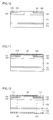
- a silicon carbide substrate 1 in the present embodiment includes a base substrate 10 composed of silicon carbide and an SiC layer 20 composed of single crystal silicon carbide different from base substrate 10 and arranged on base substrate 10 in contact therewith.
- silicon carbide substrate 1 in silicon carbide substrate 1, base substrate 10 composed of silicon carbide crystal, for example, high in fault density and low in quality can be worked to prescribed shape and size so that silicon carbide single crystal not having a desired shape or the like although being of high quality can be arranged on base substrate 10 as SiC layer 20.
- Such silicon carbide substrates 1 are uniform in prescribed shape and size, and thus more efficient manufacturing of a semiconductor device can be achieved.
- semiconductor devices can be manufactured with the use of SiC layers 20 of high quality for silicon carbide substrates 1, effective use of silicon carbide single crystal can be made. Consequently, silicon carbide substrate 1 in the present embodiment is a silicon carbide substrate allowing reduction in cost for manufacturing a semiconductor device.
- base substrate 10 is preferably composed of single crystal silicon carbide.
- difference in various physical property values from SiC layer 20 composed of single crystal silicon carbide becomes small, and hence a silicon carbide substrate stable in particular in a process for manufacturing a semiconductor device under various environments is obtained.
- SiC layer 20 is lower in micropipe density than base substrate 10. In addition, in silicon carbide substrate 1. preferably, SiC layer 20 is lower in threading screw dislocation density than base substrate 10. In addition, in silicon carbide substrate 1, preferably, SiC layer 20 is lower in threading edge dislocation density than base substrate 10. In addition, in silicon carbide substrate 1, preferably, SiC layer 20 is lower in basal plane dislocation density than base substrate 10. In addition, in silicon carbide substrate 1, preferably, SiC layer 20 is lower in composite dislocation density than base substrate 10. In addition, in silicon carbide substrate 1, preferably, SiC layer 20 is lower in stacking fault density than base substrate 10. In addition, in silicon carbide substrate 1, preferably, SiC layer 20 is lower in point defect density than base substrate 10.
- Silicon carbide substrate 1 allowing manufacturing of a semiconductor device of high quality can be obtained by thus arranging SiC layer 20 lower in fault density than base substrate 10. Further, in silicon carbide substrate 1, preferably, SiC layer 20 is smaller in a full width at half maximum of X-ray rocking curve than SiC layer 20. Thus, silicon carbide substrate 1 allowing manufacturing of a semiconductor device of high quality can be obtained by arranging SiC layer 20 smaller in a full width at half maximum of X-ray rocking curve, that is, higher in crystallinity, than base substrate 10.
- base substrate 10 may include a single crystal layer 10B composed of single crystal silicon carbide so as to include a main surface 10A on the side facing SiC layer 20.
- a region 10C of the base substrate other than single crystal layer 10B is removed to allow only single crystal layer 10B of base substrate 10 to remain in the inside of the semiconductor device.
- a semiconductor device of high quality can be manufactured while handling of silicon carbide substrate 1 in the manufacturing process is facilitated.
- SiC layer 20 is preferably lower in micropipe density than single crystal layer 10B. In addition, in silicon carbide substrate 1, preferably, SiC layer 20 is lower in threading screw dislocation density than single crystal layer 10B. In addition, in silicon carbide substrate 1, preferably, SiC layer 20 is lower in threading edge dislocation density than single crystal layer 10B.
- SiC layer 20 is lower in basal plane dislocation density than single crystal layer 10B above. In addition, in silicon carbide substrate 1 above, preferably, SiC layer 20 is lower in composite dislocation density than single crystal layer 10B. In addition, in silicon carbide substrate 1, preferably, SiC layer 20 is lower in stacking fault density than single crystal layer 10B. In addition, in silicon carbide substrate 1, preferably, SiC layer 20 is lower in point defect density than single crystal layer 10B. Thus, silicon carbide substrate 1 allowing manufacturing of a semiconductor device of high quality can be obtained by arranging SiC layer 20 lower in fault density than single crystal layer 10B of base substrate 10.
- SiC layer 20 is smaller in a full width at half maximum of X-ray rocking curve than single crystal layer 10B.
- silicon carbide substrate 1 allowing manufacturing of a semiconductor device of high quality can be obtained by arranging SiC layer 20 smaller in a full width at half maximum of X-ray rocking curve, that is, higher in crystallinity, than single crystal layer 10B of base substrate 10.
- impurity density in base substrate 10 can be not lower than 5 ⁇ 10 18 cm -3 .
- carrier density in base substrate 10 increases and silicon carbide substrate 1 suitable for manufacturing a vertical semiconductor device can be obtained.
- impurity concentration in base substrate 10 can be higher than 2 ⁇ 10 19 cm -3 .
- impurity concentration in SiC layer 20 can be higher than 5 ⁇ 10 18 cm -3 and lower than 2 ⁇ 10 19 cm -3 .
- resistivity in a direction of thickness can be lowered while suppressing generation of stacking faults caused by heat treatment.
- resistivity of base substrate 10 can be not lower than 1 ⁇ 10 5 ⁇ cm.
- a resistance value of base substrate 10 increases and silicon carbide substrate 1 suitable for manufacturing a lateral semiconductor device required to adapt to a higher frequency can be obtained.
- a main surface 20A of SiC layer 20 opposite to base substrate 10 may have an off angle with respect to a plane orientation ⁇ 0001 ⁇ not smaller than 50° and not greater than 65°.
- silicon carbide substrate 1 allowing manufacturing of a high-performance semiconductor device while making effective use of silicon carbide single crystal can be obtained.
- an angle between an off orientation of main surface 20A and a ⁇ 1-100> direction may be not greater than 5°.
- the ⁇ 1-100> direction is a representative off orientation in the silicon carbide substrate.
- variation in off orientation originating from variation or the like in slice working in the process for manufacturing silicon carbide substrate 1 to 5° or smaller, formation or the like of an epitaxially grown layer on silicon carbide substrate 1 (on main surface 20A) can be facilitated.
- an off angle of main surface 20A with respect to a ⁇ 03-38 ⁇ plane in the ⁇ 1-100> direction can be not smaller than -3° and not greater than 5°.
- channel mobility in a case where a MOSFET or the like is fabricated with silicon carbide substrate 1 can further be improved.
- an angle between an off orientation of main surface 20A and a ⁇ 11-20> direction may be not greater than 5°.
- the ⁇ 11-20> direction is a representative off orientation in a silicon carbide substrate.
- silicon carbide substrate 1 in the present embodiment preferably, main surface 20A of SiC layer 20 opposite to base substrate 10 is polished.
- an epitaxially grown layer of high quality can be formed on main surface 20A. Consequently, a semiconductor device including the epitaxially grown layer of high quality, for example, as an active layer, can be manufactured. Namely, by adopting such a structure, silicon carbide substrate 1 allowing manufacturing of a high-quality semiconductor device including an epitaxial layer formed on SiC layer 20 can be obtained.
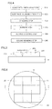
- a substrate preparation step is performed as the step (S10).
- base substrate 10 composed of silicon carbide and SiC substrate 20 composed of single crystal silicon carbide are prepared.
- a substrate planarization step is performed as the step (S20).
- step (S20) respective main surfaces (bonding surfaces) of base substrate 10 and SiC substrate 20 to be in contact with each other in the step (S30) which will be described later are planarized, for example, by polishing.
- this step (S20) is not an essential step, a size of a gap between base substrate 10 and SiC substrate 20 opposed to each other becomes uniform by performing this step and hence uniformity in reaction (bonding) in the bonding surface in the step (S40) which will be described later is improved. Consequently, base substrate 10 and SiC substrate 20 can more reliably be bonded to each other.
- surface roughness Ra of the bonding surface above is preferably less than 100 nm and preferably less than 50 nm. Moreover, by setting surface roughness Ra of the bonding surface to less than 10 nm, further reliable bonding can be achieved.
- the step (S20) may be omitted and the step (S30) may be performed without polishing respective main surfaces of base substrate 10 and SiC substrate 20 to be in contact with each other. Cost for manufacturing silicon carbide substrate 1 can thus be reduced. Further, from a point of view of removal of a damaged layer around the surface caused by slicing or the like at the time of fabrication of base substrate 10 and SiC substrate 20, for example, the step of removing the damaged layer by etching may be performed instead of or after the step (S20) above, and then the step (S30) which will be described later may be performed.
- a stacking step is performed as the step (S30).
- SiC substrate 20 is placed on the main surface of base substrate 10 in contact therewith so that a stack substrate is fabricated.
- main surface 20A of SiC substrate 20 opposite to base substrate 10 may have an off angle with respect to the ⁇ 0001 ⁇ plane not smaller than 50° and not greater than 65°.
- silicon carbide substrate 1 in which main surface 20A of SiC layer 20 has an off angle with respect to the ⁇ 0001 ⁇ plane not smaller than 50° and not greater than 65° can readily be manufactured.
- an angle between an off orientation of main surface 20A above and the ⁇ 1-100> direction may be not greater than 5°.
- an off angle of main surface 20A with respect to a ⁇ 03-38 ⁇ plane in the ⁇ 1-100> direction may be not smaller than -3° and not greater than 5°.
- channel mobility in a case where a MOSFET or the like is fabricated with manufactured silicon carbide substrate 1 can further be improved.
- an angle between an off orientation of main surface 20A and a ⁇ 11-20> direction may be not greater than 5°.
- step (S40) base substrate 10 and SiC substrate 20 are bonded to each other by heating the stack substrate above.
- silicon carbide substrate 1 in the first embodiment including bonded SiC substrate 20 as SiC layer 20 can readily be manufactured.
- the stack substrate above may be heated in an atmosphere obtained by reducing a pressure of an ambient air atmosphere. Thus, cost for manufacturing silicon carbide substrate 1 can be reduced.
- a gap formed between base substrate 10 and SiC substrate 20 is preferably not greater than 100 ⁇ m.
- uniform bonding between base substrate 10 and SiC substrate 20 can be achieved in the step (S40).
- the stack substrate above is preferably heated to a temperature range not lower than a sublimation temperature of silicon carbide.
- base substrate 10 and SiC substrate 20 can more reliably be bonded to each other.
- a gap formed between base substrate 10 and SiC substrate 20 to 100 ⁇ m or smaller in the stack substrate, equal bonding by sublimation of SiC can be achieved.
- a temperature for heating the stack substrate in the step (S40) is preferably not lower than 1800°C and not higher than 2500°C.
- a heating temperature is lower than 1800°C, it takes long time to achieve bonding between base substrate 10 and SiC substrate 20 and efficiency in manufacturing silicon carbide substrate 1 is lowered.
- a heating temperature exceeds 2500°C, respective surfaces of base substrate 10 and SiC substrate 20 roughen and more crystal defects in fabricated silicon carbide substrate 1 are likely.
- a temperature for heating the stack substrate in the step (S40) is preferably not lower than 1900°C and not higher than 2100°C.
- an atmosphere during heating in the step (S40) may be an inert gas atmosphere.
- an inert gas atmosphere containing at least one selected from the group consisting of argon, helium and nitrogen is preferred.
- the method of manufacturing silicon carbide substrate 1 in the present embodiment may further include the step of polishing a main surface of SiC substrate 20 corresponding to main surface 20A of SiC substrate 20 opposite to base substrate 10 in the stack substrate.
- silicon carbide substrate 1 in which main surface 20A of SiC layer 20 opposite to base substrate 10 is polished can be manufactured.
- the polishing step may be performed before or after bonding between base substrate 10 and SiC substrate 20, so long as it is performed after the step (S10).
- silicon carbide substrate 1 in the second embodiment has a construction similar to that of silicon carbide substrate 1 in the first embodiment, achieves a similar effect, and can be manufactured similarly. Silicon carbide substrate 1 in the second embodiment, however, is different from that in the first embodiment in that a plurality of SiC layers 20 are stacked.
- silicon carbide substrate 1 in the second embodiment includes a plurality of (two in the present embodiment) SiC layers 20 on base substrate 10.
- silicon carbide substrate 1 in the present embodiment is a silicon carbide substrate including SiC layers 20 in accordance with an intended structure of a semiconductor device. More specifically, for example when silicon carbide substrate 1 is used for manufacturing a vertical power device (vertical MOSFET; Metal Oxide Semiconductor Field Effect Transistor and the like), impurity density in base substrate 10 is preferably increased in order to lower resistivity in a direction of stack (a direction of thickness) in silicon carbide substrate 1 as much as possible.
- vertical MOSFET Metal Oxide Semiconductor Field Effect Transistor
- Silicon carbide substrate 1 according to the second embodiment can be carried out as in the first embodiment, by stacking a plurality of (two) SiC substrates 20 on base substrate 10 in the step (S30) in the method of manufacturing silicon carbide substrate 1 in the first embodiment above.
- silicon carbide substrate 1 including a plurality of SiC substrates 20 more securely bonded to one another can be manufactured.
- the steps (S10) to (S40) are performed as in the first embodiment. Thereafter, in the step (S50), a second stacking step is performed. In this step (S50), a second stack substrate is fabricated by further stacking another SiC substrate 20 on SiC substrate 20 that was stacked on base substrate 10 in the step (S30) and bonded to base substrate 10 in the step (S40).
- a second bonding step is performed as the step (S60).
- the stack substrate and another SiC substrate 20 are bonded to each other by heating the second stack substrate above as in the step (S40) above.
- respective main surfaces (bonding surfaces) of SiC substrates 20 to be in contact with each other in the step (S50) may be planarized.
- surface roughness Ra of the bonding surface above is preferably less than 100 nm and preferably less than 50 nm.
- polishing for planarization above may be omitted and the step (S50) may be performed without polishing respective main surfaces of SiC substrates 20 to be in contact with each other. Cost for manufacturing silicon carbide substrate 1 can thus be reduced.
- the step of removing the damaged layer by etching may be performed instead of or after planarization above, and then the step (S50) may be performed.
- silicon carbide substrate 1 in the third embodiment has a construction similar to that of silicon carbide substrate 1 in the first embodiment, achieves a similar effect, and can be manufactured similarly. Silicon carbide substrate 1 in the third embodiment, however, is different from that in the first embodiment in that a plurality of SiC layers 20 are two-dimensionally arranged in alignment.
- silicon carbide substrate 1 in the third embodiment a plurality of (nine in the present embodiment) SiC layers 20 are two-dimensionally arranged in alignment. Namely, a plurality of SiC layers 20 are arranged in alignment along main surface 10A of base substrate 10. More specifically, nine SiC layers 20 are arranged in matrix such that SiC layers 20 adjacent on base substrate 10 are in contact with one another.
- silicon carbide substrate 1 in the present embodiment is silicon carbide substrate 1 that can be handled as a large-diameter substrate having high-quality SiC layers 20. Then, by employing this silicon carbide substrate 1, a process for manufacturing a semiconductor device can be more efficient. Referring again to Fig.
- respective end surfaces 20B of adjacent SiC layers 20 are substantially perpendicular to main surface 20A of SiC layer 20.
- silicon carbide substrate 1 in the present embodiment can readily be manufactured. It is noted that silicon carbide substrate 1 in the third embodiment can be manufactured as in the first embodiment by two-dimensionally arranging in alignment a plurality of SiC substrates 20 of which end surfaces 20B are substantially perpendicular to main surface 20A in the step (S30).
- SiC layer 20 may be arranged on base substrate 10 and a plurality of SiC layers 20 are two-dimensionally arranged in alignment on SiC layer 20.
- Such silicon carbide substrate 1 can be manufactured by two-dimensionally placing in alignment a plurality of SiC substrates 20 of which end surfaces 20B are substantially perpendicular to main surface 20A in the step (S50) in the manufacturing method described with reference to Fig. 4 in the second embodiment above.
- silicon carbide forming SiC layer 20 preferably has a hexagonal crystal structure and the crystal structure is more preferably 4H-SiC.
- base substrate 10 and SiC layer 20 are preferably composed of silicon carbide single crystal identical in crystal structure.
- an angle between c axes of silicon carbide single crystals forming them is preferably smaller than 1° and more preferably smaller than 0.1°. Furthermore, preferably, a c plane of silicon carbide single crystal does not rotate in the plane.
- Base substrate 10 has a diameter preferably not smaller than 2 inches and more preferably not smaller than 6 inches.
- silicon carbide substrate 1 has a thickness preferably not smaller than 200 ⁇ m and not greater than 1000 ⁇ m, and more preferably not smaller than 300 ⁇ m and not greater than 700 ⁇ m.
- SiC layer 20 has resistivity preferably not higher than 50 m ⁇ cm and more preferably not higher than 20 m ⁇ cm.
- a semiconductor device 101 is a vertical DiMOSFET (Double Implanted MOSFET), and includes a substrate 102, a buffer layer 121, a breakdown voltage holding layer 122, a p region 123, an n + region 124, a p + region 125, an oxide film 126, a source electrode 111 and an upper source electrode 127, a gate electrode 110, and a drain electrode 112 formed on a back surface side of substrate 102.
- a vertical DiMOSFET Double Implanted MOSFET
- buffer layer 121 composed of silicon carbide is formed on a surface of substrate 102 composed of silicon carbide having an n conductivity type.
- a silicon carbide substrate according to the present invention including silicon carbide substrate 1 described in the first to third embodiments above is adopted as substrate 102.
- buffer layer 121 is formed on SiC layer 20 of silicon carbide substrate 1.
- Buffer layer 121 has an n conductivity type and a thickness, for example, of 0.5 ⁇ m.
- density of an n-type conductive impurity in buffer layer 121 can be, for example, 5 ⁇ 10 17 cm -3 .
- Breakdown voltage holding layer 122 is formed on this buffer layer 121.
- This breakdown voltage holding layer 122 is composed of silicon carbide having an n conductivity type and it has a thickness, for example, of 10 ⁇ m. In addition, such a value as 5 ⁇ 10 15 cm -3 can be adopted as density of an n-type conductive impurity in breakdown voltage holding layer 122.
- p regions 123 having a p conductivity type are formed at a distance from one another.
- n + region 124 is formed in a surface layer of p region 123.
- p + region 125 is formed at a position adjacent to this n + region 124.
- Oxide film 126 is formed to extend from n + region 124 in one p region 123 to p region 123, breakdown voltage holding layer 122 exposed between two p regions 123, the other p region 123, and n + region 124 in the other p region 123.
- Gate electrode 110 is formed on oxide film 126.
- source electrode 111 is formed on n + region 124 and p + region 125.
- Upper source electrode 127 is formed on this source electrode 111.
- drain electrode 112 is formed on the back surface which is a surface opposite to a front surface where buffer layer 121 is formed.
- semiconductor device 101 in the present embodiment a silicon carbide substrate according to the present invention such as silicon carbide substrate 1 described in the first to third embodiments above is adopted as substrate 102.
- semiconductor device 101 includes substrate 102 which is a silicon carbide substrate, buffer layer 121 and breakdown voltage holding layer 122 as epitaxially grown and formed on substrate 102, and source electrode 111 formed on breakdown voltage holding layer 122.
- This substrate 102 is a silicon carbide substrate according to the present invention such as silicon carbide substrate 1.
- the silicon carbide substrate according to the present invention is a silicon carbide substrate allowing reduction in cost for manufacturing a semiconductor device. Therefore, semiconductor device 101 is a semiconductor device of which manufacturing cost has been reduced.
- a substrate preparation step (S 110) is performed.
- substrate 102 (see Fig. 9 ) composed of silicon carbide having, for example, a (03-313) plane as the main surface is prepared.
- a substrate for example, having an n conductivity type and a substrate resistance of 0.02 ⁇ cm may be employed as this substrate 102 (see Fig. 9 ).
- an epitaxial layer formation step (S120) is performed. Specifically, buffer layer 121 is formed on the surface of substrate 102. This buffer layer 121 is formed on SiC layer 20 (see Figs. 1, 3 , and 5 ) of silicon carbide substrate 1 adopted as substrate 102. An epitaxial layer composed of silicon carbide having an n conductivity type and having a thickness, for example, of 0.5 ⁇ m is formed as buffer layer 121. For example, such a value as 5 ⁇ 10 17 cm -3 can be adopted as density of a conductive impurity in buffer layer 121. Then, as shown in Fig. 9 , breakdown voltage holding layer 122 is formed on this buffer layer 121.
- a layer composed of silicon carbide having an n conductivity type is formed as this breakdown voltage holding layer 122 with an epitaxial growth method.
- a value as 10 ⁇ m can be adopted as a thickness of this breakdown voltage holding layer 122.
- a value as 5 ⁇ 10 15 cm -3 can be adopted as density of an n-type conductive impurity in this breakdown voltage holding layer 122.
- an implantation step (S 130) is performed. Specifically, using an oxide film formed with photolithography and etching as a mask, an impurity having a p conductivity type is implanted into breakdown voltage holding layer 122, to thereby form p region 123 as shown in Fig. 10 . After the used oxide film is removed, an oxide film having a new pattern is again formed with photolithography and etching. Then, using this oxide film as a mask, an n-type conductive impurity is implanted into a prescribed region to thereby form n + region 124. By implanting a conductive impurity having a p conductivity type with the similar technique, p + region 125 is formed. Consequently, a structure as shown in Fig. 10 is obtained.
- activation annealing treatment is performed.
- an argon gas is used as an atmospheric gas and such conditions as a heating temperature of 1700°C and a heating time period of 30 minutes can be employed.
- a gate insulating film formation step (S140) is performed. Specifically, as shown in Fig. 11 , oxide film 126 is formed to cover breakdown voltage holding layer 122, p region 123, n + region 124, and p + region 125.
- oxide film 126 is formed to cover breakdown voltage holding layer 122, p region 123, n + region 124, and p + region 125.
- dry oxidation thermal oxidation
- Such conditions as a heating temperature of 1200°C and a heating time period of 30 minutes can be employed as conditions in this dry oxidation.
- a nitrogen annealing step (S 150) is performed. Specifically, annealing treatment is performed with nitrogen monoxide (NO) being employed as an atmospheric gas. As a temperature condition for annealing treatment, for example, a heating temperature of 1100°C and a heating time period of 120 minutes are set. Consequently, nitrogen atoms are introduced in the vicinity of an interface between oxide film 126 and each of breakdown voltage holding layer 122, p region 123, n + region 124, and p + region 125 located below. After this annealing step using nitrogen monoxide as the atmospheric gas, annealing using an argon (Ar) gas which is an inert gas may further be performed. Specifically, an argon gas is used as an atmospheric gas and such conditions as a heating temperature of 1100°C and a heating time period of 60 minutes may be adopted.
- an electrode formation step (S 160) is performed. Specifically, a resist film having a pattern is formed on oxide film 126 with photolithography. Using this resist film as a mask, a portion of the oxide film located on n + region 124 and p + region 125 is etched away. Thereafter, a conductor film made of a metal or the like is formed on the resist film and in an opening formed in oxide film 126, to be in contact with n + region 124 and p + region 125. Thereafter, by removing the resist film, the conductor film that has been located on the resist film is removed (lift-off).
- nickel (Ni) can be used as the conductor. Consequently, as shown in Fig.
- heat treatment for alloying is preferably performed here. Specifically, heat treatment (alloying treatment) using, for example, an argon (Ar) gas representing an inert gas as an atmospheric gas, with a heating temperature being set to 950°C and a heating time period being set to 2 minutes, is performed.
- Ar argon
- upper source electrode 127 (see Fig. 7 ) is formed on source electrode 111.
- gate electrode 110 (see Fig. 7 ) is formed on oxide film 126. Semiconductor device 101 shown in Fig. 7 can thus be obtained.
- a vertical MOSFET has been described in the fourth embodiment above by way of example of a semiconductor device that can be fabricated with a silicon carbide substrate according to the present invention
- a semiconductor device that can be fabricated is not limited thereto.
- various semiconductor devices such as a JFET (Junction Field Effect Transistor), an IGBT (Insulated Gate Bipolar Transistor), and a Schottky barrier diode can be fabricated with the silicon carbide substrate according to the present invention.
- a crystal plane that can be adopted as the main surface above is not limited thereto and any crystal plane in accordance with applications including the (0001) plane can be adopted as the main surface above.
- Example 1 according to the present invention will be described below.
- Various substrates composed of silicon carbide single crystal were prepared and experiments for examining whether substrates could be bonded to each other or not with a heating temperature being varied were conducted.
- An experiment procedure is as follows.
- a silicon carbide substrate can be manufactured by bonding substrates different in fault density, conductivity (impurity density) and poly type to each other and a silicon carbide substrate can be manufactured by bonding three substrates as they are stacked.
- Warpage in sample C in which substrates 1,2 and 3 having n-type impurity densities of 9 ⁇ 10 18 cm -3 , 3 ⁇ 10 19 cm -3 and 1 ⁇ 10 20 cm -3 respectively were bonded in this order was 10 ⁇ m.
- a sample in which substrate 1 and substrate 3 were directly bonded to each other was also fabricated, and its warpage was 50 ⁇ m. Based on this fact, it was confirmed that warpage of the bonded substrate could be lessened by bonding a substrate high in impurity density and a substrate low in impurity density with another substrate having impurity density intermediate therebetween being interposed so that a lattice constant gradually varied in a direction of thickness of the obtained bonded substrate.
- Example 2 according to the present invention will be described below.
- An experiment for studying whether substrates of which respective main surfaces were greatly inclined with respect to the (0001) plane (substrates each having a main surface of which off angle with respect to plane orientation ⁇ 0001 ⁇ was not smaller than 50° and not greater than 65°) could be bonded to each other or not and whether a substrate of which main surface was greatly inclined with respect to the (0001) plane and a substrate having the (0001) plane as the main surface could be bonded to each other or not was conducted.
- An experiment procedure is as follows.
- two substrates base substrate 10 and SiC substrate 20
- base substrate 10 and SiC substrate 20 each composed of SiC and having the (03-38) plane as the main surface were prepared.
- the two substrates were layered such that the main surfaces were in contact with each other to fabricate the stack substrate.
- the stack substrate was heated to 2100°C which was equal to or higher than a sublimation temperature of SiC so that the two substrates were bonded to each other under such a condition as holding for 30 hours in a nitrogen gas atmosphere at a pressure of 1 Pa.
- a silicon carbide substrate was thus fabricated.
- a temperature of base substrate 10 was maintained at a temperature slightly higher than that of SiC substrate 20.
- crystal orientation in a cross-section perpendicular to the bonding surface of the obtained silicon carbide substrate was examined with an electron back scatter diffraction (EBSD) method.
- EBSD electron back scatter diffraction
- SiC crystal forming base substrate 10 and SiC crystal forming SiC layer 20 were identical in crystal orientation as a result of the fact that bonding between base substrate 10 and SiC substrate 20 was achieved by sublimation of base substrate 10 held at a temperature slightly higher than SiC substrate 20.
- Example 3 An experiment for examining relation between a size of a gap formed between the base substrate and the SiC substrate during bonding of the stack substrate and a state of bonding of the stack substrate was conducted. Initially, as in the case of Example 3 above, the two substrates (base substrate 10 and SiC substrate 20) were prepared and two substrates were layered such that main surfaces thereof were brought in contact with each other. The stack substrate was thus fabricated. Here, adjustment was made such that a gap formed between the two substrates was from 0.5 to 1000 ⁇ m wide. Then, as in Example 3 above, the stack substrate above was heated to 2100°C and held for 30 hours in a nitrogen gas atmosphere at a pressure of 1 Pa. Then, a state of bonding of the stack substrate after the treatment was checked. Table 3 shows results of the experiment. Table 3 Gap ( ⁇ m) 0.5 1 10 50 100 200 1000 State of Bonding A A A A A B C A: uniform bonding B: partial bonding C: bonding unsuccessful
- a semiconductor device can be fabricated with the silicon carbide substrate according to the present invention.
- an epitaxially grown layer serving as an operating layer is formed on the silicon carbide substrate manufactured with the method of manufacturing a silicon carbide substrate according to the present invention above.
- an epitaxially grown layer serving as an operating layer is formed on the silicon carbide substrate according to the present invention above.
- the semiconductor device according to the present invention includes the silicon carbide substrate according to the present invention above, an epitaxially grown layer formed on the silicon carbide substrate, and an electrode formed on the epitaxially grown layer.
- the semiconductor device includes a base substrate composed of silicon carbide, an SiC layer composed of single crystal silicon carbide and arranged on the base substrate in contact therewith, an epitaxially grown layer formed on the SiC layer, and an electrode formed on the epitaxially grown layer.
- a silicon carbide substrate and a method of manufacturing the same according to the present invention are particularly advantageously applicable to a silicon carbide substrate used for manufacturing a semiconductor device required to be low in manufacturing cost and a method of manufacturing the same.
- a semiconductor device according to the present invention is particularly advantageously applicable to a semiconductor device required to be low in manufacturing cost.
- silicon carbide substrate 10 base substrate; 10A main surface; 20 SiC layer (SiC substrate); 20A main surface; 20B end surface; 30 boundary; 101 semiconductor device; 102 substrate; 110 gate electrode; 111 source electrode; 112 drain electrode; 121 buffer layer; 122 breakdown voltage holding layer; 123 p region; 124 n + region; 125 p + region; 126 oxide film; and 127 upper source electrode.
Landscapes
- Chemical & Material Sciences (AREA)
- Engineering & Computer Science (AREA)
- Crystallography & Structural Chemistry (AREA)
- Materials Engineering (AREA)
- Metallurgy (AREA)
- Organic Chemistry (AREA)
- Inorganic Chemistry (AREA)
- Recrystallisation Techniques (AREA)
- Crystals, And After-Treatments Of Crystals (AREA)
- Electrodes Of Semiconductors (AREA)
Applications Claiming Priority (5)
| Application Number | Priority Date | Filing Date | Title |
|---|---|---|---|
| JP2009114737 | 2009-05-11 | ||
| JP2009219065 | 2009-09-24 | ||
| JP2009229764 | 2009-10-01 | ||
| JP2009248621 | 2009-10-29 | ||
| PCT/JP2010/057439 WO2010131568A1 (fr) | 2009-05-11 | 2010-04-27 | Substrat en carbure de silicium, dispositif à semi-conducteurs et procédé de fabrication de substrat en carbure de silicium |
Publications (2)
| Publication Number | Publication Date |
|---|---|
| EP2432000A1 true EP2432000A1 (fr) | 2012-03-21 |
| EP2432000A4 EP2432000A4 (fr) | 2012-11-21 |
Family
ID=43084945
Family Applications (5)
| Application Number | Title | Priority Date | Filing Date |
|---|---|---|---|
| EP10774826A Withdrawn EP2432000A4 (fr) | 2009-05-11 | 2010-04-27 | Substrat en carbure de silicium, dispositif à semi-conducteurs et procédé de fabrication de substrat en carbure de silicium |
| EP10774828A Withdrawn EP2432002A4 (fr) | 2009-05-11 | 2010-04-27 | Substrat de carbure de silicium et dispositif semi-conducteur |
| EP10774831A Withdrawn EP2432022A1 (fr) | 2009-05-11 | 2010-04-27 | Transistor bipolaire de type à grille isolante (igbt) |
| EP10774827A Ceased EP2432001A4 (fr) | 2009-05-11 | 2010-04-27 | Procédé de production de substrat semi-conducteur |
| EP10774830.3A Withdrawn EP2432020A4 (fr) | 2009-05-11 | 2010-04-27 | Dispositif à semi-conducteurs |
Family Applications After (4)
| Application Number | Title | Priority Date | Filing Date |
|---|---|---|---|
| EP10774828A Withdrawn EP2432002A4 (fr) | 2009-05-11 | 2010-04-27 | Substrat de carbure de silicium et dispositif semi-conducteur |
| EP10774831A Withdrawn EP2432022A1 (fr) | 2009-05-11 | 2010-04-27 | Transistor bipolaire de type à grille isolante (igbt) |
| EP10774827A Ceased EP2432001A4 (fr) | 2009-05-11 | 2010-04-27 | Procédé de production de substrat semi-conducteur |
| EP10774830.3A Withdrawn EP2432020A4 (fr) | 2009-05-11 | 2010-04-27 | Dispositif à semi-conducteurs |
Country Status (8)
| Country | Link |
|---|---|
| US (5) | US20120056202A1 (fr) |
| EP (5) | EP2432000A4 (fr) |
| JP (5) | JP5344037B2 (fr) |
| KR (5) | KR20120014024A (fr) |
| CN (5) | CN102422425A (fr) |
| CA (5) | CA2761428A1 (fr) |
| TW (5) | TW201120939A (fr) |
| WO (5) | WO2010131570A1 (fr) |
Cited By (1)
| Publication number | Priority date | Publication date | Assignee | Title |
|---|---|---|---|---|
| EP4044212A4 (fr) * | 2019-11-14 | 2022-11-23 | Huawei Digital Power Technologies Co., Ltd. | Substrat semi-conducteur, son procédé de fabrication, et dispositif semi-conducteur |
Families Citing this family (59)
| Publication number | Priority date | Publication date | Assignee | Title |
|---|---|---|---|---|
| SG164324A1 (en) * | 2009-02-20 | 2010-09-29 | Semiconductor Energy Lab | Semiconductor device and manufacturing method of the same |
| CN102422425A (zh) | 2009-05-11 | 2012-04-18 | 住友电气工业株式会社 | 绝缘栅双极晶体管 |
| US20120015499A1 (en) * | 2009-11-13 | 2012-01-19 | Sumitomo Electric Industries, Ltd. | Method for manufacturing semiconductor substrate |
| CA2759074A1 (fr) * | 2010-02-05 | 2011-08-11 | Taro Nishiguchi | Procede de production de substrat en carbure de silicium |
| JP2011246315A (ja) * | 2010-05-28 | 2011-12-08 | Sumitomo Electric Ind Ltd | 炭化珪素基板およびその製造方法 |
| JP5447206B2 (ja) * | 2010-06-15 | 2014-03-19 | 住友電気工業株式会社 | 炭化珪素単結晶の製造方法および炭化珪素基板 |
| JPWO2012127748A1 (ja) * | 2011-03-22 | 2014-07-24 | 住友電気工業株式会社 | 炭化珪素基板 |
| JP2012201543A (ja) * | 2011-03-25 | 2012-10-22 | Sumitomo Electric Ind Ltd | 炭化珪素基板 |
| JP2013018693A (ja) * | 2011-06-16 | 2013-01-31 | Sumitomo Electric Ind Ltd | 炭化珪素基板およびその製造方法 |
| DE112012003260T5 (de) | 2011-08-05 | 2014-05-15 | Sumitomo Electric Industries, Ltd. | Substrat, Halbleitervorrichtung und Verfahren zur Herstellung derselben |
| WO2013073216A1 (fr) * | 2011-11-14 | 2013-05-23 | 住友電気工業株式会社 | Substrat de carbure de silicium, dispositif semi-conducteur et procédés de production de ces derniers |
| KR101984698B1 (ko) * | 2012-01-11 | 2019-05-31 | 삼성전자주식회사 | 기판 구조체, 이로부터 제조된 반도체소자 및 그 제조방법 |
| JP6119100B2 (ja) | 2012-02-01 | 2017-04-26 | 住友電気工業株式会社 | 炭化珪素半導体装置 |
| TWI456737B (zh) * | 2012-03-05 | 2014-10-11 | Richtek Technology Corp | 垂直式半導體元件及其製造方法 |
| CN103325747A (zh) * | 2012-03-19 | 2013-09-25 | 立锜科技股份有限公司 | 垂直式半导体元件及其制造方法 |
| JP5884585B2 (ja) * | 2012-03-21 | 2016-03-15 | 住友電気工業株式会社 | 炭化珪素半導体装置の製造方法 |
| US9466552B2 (en) * | 2012-03-30 | 2016-10-11 | Richtek Technology Corporation | Vertical semiconductor device having a non-conductive substrate and a gallium nitride layer |
| KR101386119B1 (ko) * | 2012-07-26 | 2014-04-21 | 한국전기연구원 | SiC MOSFET의 오믹 접합 형성방법 |
| US9184229B2 (en) * | 2012-07-31 | 2015-11-10 | Kabushiki Kaisha Toshiba | Semiconductor device and method for manufacturing same |
| US8860040B2 (en) | 2012-09-11 | 2014-10-14 | Dow Corning Corporation | High voltage power semiconductor devices on SiC |
| US9018639B2 (en) | 2012-10-26 | 2015-04-28 | Dow Corning Corporation | Flat SiC semiconductor substrate |
| US9017804B2 (en) | 2013-02-05 | 2015-04-28 | Dow Corning Corporation | Method to reduce dislocations in SiC crystal growth |
| US9797064B2 (en) | 2013-02-05 | 2017-10-24 | Dow Corning Corporation | Method for growing a SiC crystal by vapor deposition onto a seed crystal provided on a support shelf which permits thermal expansion |
| US9738991B2 (en) | 2013-02-05 | 2017-08-22 | Dow Corning Corporation | Method for growing a SiC crystal by vapor deposition onto a seed crystal provided on a supporting shelf which permits thermal expansion |
| JP6297783B2 (ja) * | 2013-03-08 | 2018-03-20 | 住友電気工業株式会社 | 炭化珪素半導体装置およびその製造方法 |
| US8940614B2 (en) | 2013-03-15 | 2015-01-27 | Dow Corning Corporation | SiC substrate with SiC epitaxial film |
| JP6119564B2 (ja) | 2013-11-08 | 2017-04-26 | 住友電気工業株式会社 | 炭化珪素半導体装置の製造方法 |
| JP6356428B2 (ja) * | 2014-02-17 | 2018-07-11 | 株式会社東芝 | 半導体装置およびその製造方法 |
| CN103855206A (zh) * | 2014-02-18 | 2014-06-11 | 宁波达新半导体有限公司 | 绝缘栅双极晶体管及其制造方法 |
| JP2015176995A (ja) * | 2014-03-14 | 2015-10-05 | 株式会社東芝 | 半導体装置およびその製造方法 |
| JP6180978B2 (ja) * | 2014-03-20 | 2017-08-16 | 株式会社東芝 | 半導体装置およびその製造方法 |
| US9279192B2 (en) | 2014-07-29 | 2016-03-08 | Dow Corning Corporation | Method for manufacturing SiC wafer fit for integration with power device manufacturing technology |
| JPWO2016059670A1 (ja) * | 2014-10-14 | 2017-04-27 | 三菱電機株式会社 | 炭化珪素エピタキシャルウエハの製造方法 |
| CN104465721B (zh) * | 2014-12-05 | 2019-05-14 | 国家电网公司 | 一种碳化硅外延材料及其制备方法 |
| JP2017059600A (ja) * | 2015-09-14 | 2017-03-23 | 株式会社東芝 | 半導体装置及びその製造方法 |
| JP6696499B2 (ja) * | 2015-11-24 | 2020-05-20 | 住友電気工業株式会社 | 炭化珪素エピタキシャル基板および炭化珪素半導体装置の製造方法 |
| CN105679647B (zh) * | 2015-12-31 | 2018-06-29 | 清华大学 | 具有原子级平整表面的衬底的制备方法 |
| WO2018016171A1 (fr) * | 2016-07-21 | 2018-01-25 | 三菱電機株式会社 | Dispositif à semi-conducteur au carbure de silicium et procédé de fabrication de dispositif à semi-conducteur au carbure de silicium |
| JP6703915B2 (ja) * | 2016-07-29 | 2020-06-03 | 富士電機株式会社 | 炭化珪素半導体基板、炭化珪素半導体基板の製造方法、半導体装置および半導体装置の製造方法 |
| KR101866869B1 (ko) * | 2016-08-18 | 2018-06-14 | 주식회사 티씨케이 | SiC 소재 및 SiC 복합 소재 |
| CN110214363B (zh) * | 2017-01-31 | 2023-07-28 | 住友电气工业株式会社 | 碳化硅外延衬底和制造碳化硅半导体器件的方法 |
| DE112017006972T5 (de) * | 2017-01-31 | 2019-10-17 | Sumitomo Electric Industries, Ltd. | Siliziumcarbid-Epitaxiesubstrat und Verfahren zur Herstellung einer Siliziumcarbid-Halbleitervorrichtung |
| JP6883745B2 (ja) * | 2017-03-24 | 2021-06-09 | パナソニックIpマネジメント株式会社 | 半導体装置およびその製造方法 |
| WO2019143733A1 (fr) | 2018-01-16 | 2019-07-25 | Ipower Semiconductor | Dispositifs igbt auto-alignés et robustes |
| WO2019157222A1 (fr) * | 2018-02-07 | 2019-08-15 | Ipower Semiconductor | Dispositifs igbt à structures arrière 3d pour arrêt de champ et conduction inverse |
| KR102649978B1 (ko) | 2018-05-03 | 2024-03-22 | 엘지전자 주식회사 | 정수기의 제어 방법 |
| JP7239182B2 (ja) * | 2018-10-16 | 2023-03-14 | 山▲東▼天岳先▲進▼科技股▲フン▼有限公司 | 高純度炭化ケイ素単結晶基板及びその製造方法、応用 |
| JP7143769B2 (ja) * | 2019-01-10 | 2022-09-29 | 三菱電機株式会社 | 炭化珪素半導体基板の製造方法及び炭化珪素半導体装置の製造方法 |
| KR102150520B1 (ko) * | 2019-06-21 | 2020-09-01 | 주식회사 티씨케이 | Cvd 방식으로 형성된 sic 구조체 |
| JP7410478B2 (ja) * | 2019-07-11 | 2024-01-10 | 富士電機株式会社 | 炭化珪素半導体装置および炭化珪素半導体装置の製造方法 |
| WO2021020574A1 (fr) * | 2019-08-01 | 2021-02-04 | ローム株式会社 | Substrat semi-conducteur , dispositif à semi-conducteur et leurs procédés de production |
| JP7478604B2 (ja) | 2020-06-26 | 2024-05-07 | 株式会社日立製作所 | 半導体装置およびその製造方法 |
| US11821105B2 (en) * | 2020-07-27 | 2023-11-21 | Globalwafers Co., Ltd. | Silicon carbide seed crystal and method of manufacturing silicon carbide ingot |
| KR102442732B1 (ko) * | 2021-11-05 | 2022-09-13 | 주식회사 쎄닉 | 탄화규소 웨이퍼 및 이의 제조방법 |
| TWI831512B (zh) * | 2022-12-09 | 2024-02-01 | 鴻揚半導體股份有限公司 | 半導體裝置和其形成方法 |
| TWI912574B (zh) * | 2023-01-10 | 2026-01-21 | 中國砂輪企業股份有限公司 | 複合式基板及複合式基板之製備方法 |
| JP2024104186A (ja) * | 2023-01-23 | 2024-08-02 | 株式会社デンソー | 炭化珪素基板、炭化珪素ウェハ、炭化珪素半導体装置 |
| US12590385B2 (en) | 2023-11-07 | 2026-03-31 | Resonac Corporation | SiC epitaxial wafer |
| CN119967882A (zh) | 2023-11-07 | 2025-05-09 | 株式会社力森诺科 | SiC外延晶片 |
Family Cites Families (56)
| Publication number | Priority date | Publication date | Assignee | Title |
|---|---|---|---|---|
| JPH0637276B2 (ja) * | 1988-01-18 | 1994-05-18 | 株式会社豊田自動織機製作所 | 上下移動機構付プッシャー装置 |
| JP2846986B2 (ja) | 1991-10-30 | 1999-01-13 | 三菱マテリアル株式会社 | 半導体ウェーハの製造方法 |
| JPH0748198A (ja) * | 1993-08-05 | 1995-02-21 | Sumitomo Electric Ind Ltd | ダイヤモンドの合成法 |
| JPH10223835A (ja) * | 1997-02-05 | 1998-08-21 | Hitachi Ltd | 半導体装置とその製造方法 |
| JP2961522B2 (ja) * | 1997-06-11 | 1999-10-12 | 日本ピラー工業株式会社 | 半導体電子素子用基板およびその製造方法 |
| US6153166A (en) * | 1997-06-27 | 2000-11-28 | Nippon Pillar Packing Co., Ltd. | Single crystal SIC and a method of producing the same |
| JP3254559B2 (ja) | 1997-07-04 | 2002-02-12 | 日本ピラー工業株式会社 | 単結晶SiCおよびその製造方法 |
| JPH1187200A (ja) * | 1997-09-05 | 1999-03-30 | Toshiba Corp | 半導体基板及び半導体装置の製造方法 |
| JP2939615B2 (ja) | 1998-02-04 | 1999-08-25 | 日本ピラー工業株式会社 | 単結晶SiC及びその製造方法 |
| US6246076B1 (en) * | 1998-08-28 | 2001-06-12 | Cree, Inc. | Layered dielectric on silicon carbide semiconductor structures |
| JP2000277405A (ja) * | 1999-03-29 | 2000-10-06 | Meidensha Corp | 半導体素子の製造方法 |
| DE60033829T2 (de) * | 1999-09-07 | 2007-10-11 | Sixon Inc. | SiC-HALBLEITERSCHEIBE, SiC-HALBLEITERBAUELEMENT SOWIE HERSTELLUNGSVERFAHREN FÜR EINE SiC-HALBLEITERSCHEIBE |
| JP2002015619A (ja) | 2000-06-29 | 2002-01-18 | Kyocera Corp | 導電性材及びそれを用いた耐プラズマ部材及び半導体製造用装置 |
| JP4843854B2 (ja) * | 2001-03-05 | 2011-12-21 | 住友電気工業株式会社 | Mosデバイス |
| US6909119B2 (en) * | 2001-03-15 | 2005-06-21 | Cree, Inc. | Low temperature formation of backside ohmic contacts for vertical devices |
| JP4802380B2 (ja) * | 2001-03-19 | 2011-10-26 | 株式会社デンソー | 半導体基板の製造方法 |
| DE10247017B4 (de) * | 2001-10-12 | 2009-06-10 | Denso Corp., Kariya-shi | SiC-Einkristall, Verfahren zur Herstellung eines SiC-Einkristalls, SiC-Wafer mit einem Epitaxiefilm und Verfahren zur Herstellung eines SiC-Wafers, der einen Epitaxiefilm aufweist |
| JP3559971B2 (ja) * | 2001-12-11 | 2004-09-02 | 日産自動車株式会社 | 炭化珪素半導体装置およびその製造方法 |
| FR2834123B1 (fr) * | 2001-12-21 | 2005-02-04 | Soitec Silicon On Insulator | Procede de report de couches minces semi-conductrices et procede d'obtention d'une plaquette donneuse pour un tel procede de report |
| US6562127B1 (en) * | 2002-01-16 | 2003-05-13 | The United States Of America As Represented By The Secretary Of The Navy | Method of making mosaic array of thin semiconductor material of large substrates |
| US8080826B1 (en) * | 2002-02-14 | 2011-12-20 | Rf Micro Devices, Inc. | High performance active and passive structures based on silicon material bonded to silicon carbide |
| US20040144301A1 (en) * | 2003-01-24 | 2004-07-29 | Neudeck Philip G. | Method for growth of bulk crystals by vapor phase epitaxy |
| US7892356B2 (en) * | 2003-01-28 | 2011-02-22 | Sumitomo Electric Industries, Ltd. | Diamond composite substrate and process for producing the same |
| JP4730097B2 (ja) * | 2003-06-13 | 2011-07-20 | 住友電気工業株式会社 | 電界効果トランジスタ |
| JP4238357B2 (ja) | 2003-08-19 | 2009-03-18 | 独立行政法人産業技術総合研究所 | 炭化珪素エピタキシャルウエハ、同ウエハの製造方法及び同ウエハ上に作製された半導体装置 |
| JP4219800B2 (ja) | 2003-12-22 | 2009-02-04 | 株式会社豊田中央研究所 | SiC単結晶の製造方法 |
| CN100433256C (zh) * | 2004-03-18 | 2008-11-12 | 克里公司 | 减少堆垛层错成核位置的顺序光刻方法和具有减少的堆垛层错成核位置的结构 |
| JP4874527B2 (ja) * | 2004-04-01 | 2012-02-15 | トヨタ自動車株式会社 | 炭化珪素半導体基板及びその製造方法 |
| JP4442366B2 (ja) | 2004-08-27 | 2010-03-31 | 住友電気工業株式会社 | エピタキシャルSiC膜とその製造方法およびSiC半導体デバイス |
| JP4733485B2 (ja) * | 2004-09-24 | 2011-07-27 | 昭和電工株式会社 | 炭化珪素単結晶成長用種結晶の製造方法、炭化珪素単結晶成長用種結晶、炭化珪素単結晶の製造方法、および炭化珪素単結晶 |
| US7314520B2 (en) | 2004-10-04 | 2008-01-01 | Cree, Inc. | Low 1c screw dislocation 3 inch silicon carbide wafer |
| JP2006228961A (ja) | 2005-02-17 | 2006-08-31 | Toyota Central Res & Dev Lab Inc | 半導体装置 |
| JPWO2006114999A1 (ja) * | 2005-04-18 | 2008-12-18 | 国立大学法人京都大学 | 化合物半導体装置及び化合物半導体製造方法 |
| JP4775102B2 (ja) * | 2005-05-09 | 2011-09-21 | 住友電気工業株式会社 | 半導体装置の製造方法 |
| US7391058B2 (en) * | 2005-06-27 | 2008-06-24 | General Electric Company | Semiconductor devices and methods of making same |
| JP2008004726A (ja) * | 2006-06-22 | 2008-01-10 | Matsushita Electric Ind Co Ltd | 半導体素子およびその製造方法 |
| JP4916247B2 (ja) * | 2006-08-08 | 2012-04-11 | トヨタ自動車株式会社 | 炭化珪素半導体装置及びその製造方法 |
| CN100438083C (zh) * | 2006-12-23 | 2008-11-26 | 厦门大学 | δ掺杂4H-SiC PIN结构紫外光电探测器及其制备方法 |
| JP4748067B2 (ja) | 2007-01-15 | 2011-08-17 | 株式会社デンソー | 炭化珪素単結晶の製造方法および製造装置 |
| JP2008226997A (ja) | 2007-03-09 | 2008-09-25 | Sumitomo Electric Ind Ltd | 半導体装置およびその製造方法 |
| JP2008235776A (ja) * | 2007-03-23 | 2008-10-02 | Sumco Corp | 貼り合わせウェーハの製造方法 |
| WO2008120469A1 (fr) * | 2007-03-29 | 2008-10-09 | Panasonic Corporation | Procédé permettant de fabriquer un élément semi-conducteur de carbure de silicium |
| WO2008120467A1 (fr) * | 2007-03-29 | 2008-10-09 | Panasonic Corporation | Procédé de fabrication d'un dispositif semi-conducteur |
| FR2914488B1 (fr) * | 2007-03-30 | 2010-08-27 | Soitec Silicon On Insulator | Substrat chauffage dope |
| JP2008280207A (ja) | 2007-05-10 | 2008-11-20 | Matsushita Electric Ind Co Ltd | SiC単結晶基板の製造方法 |
| JP2009117533A (ja) * | 2007-11-05 | 2009-05-28 | Shin Etsu Chem Co Ltd | 炭化珪素基板の製造方法 |
| JP5157843B2 (ja) * | 2007-12-04 | 2013-03-06 | 住友電気工業株式会社 | 炭化ケイ素半導体装置およびその製造方法 |
| JP5504597B2 (ja) * | 2007-12-11 | 2014-05-28 | 住友電気工業株式会社 | 炭化ケイ素半導体装置およびその製造方法 |
| JP2010184833A (ja) * | 2009-02-12 | 2010-08-26 | Denso Corp | 炭化珪素単結晶基板および炭化珪素単結晶エピタキシャルウェハ |
| CN102422425A (zh) | 2009-05-11 | 2012-04-18 | 住友电气工业株式会社 | 绝缘栅双极晶体管 |
| TW201104860A (en) | 2009-05-11 | 2011-02-01 | Sumitomo Electric Industries | Semiconductor device |
| US20120070605A1 (en) | 2009-09-24 | 2012-03-22 | Sumitomo Electric Industries, Ltd. | Silicon carbide ingot, silicon carbide substrate, manufacturing method thereof, crucible, and semiconductor substrate |
| US20110221039A1 (en) * | 2010-03-12 | 2011-09-15 | Sinmat, Inc. | Defect capping for reduced defect density epitaxial articles |
| JP2011233638A (ja) * | 2010-04-26 | 2011-11-17 | Sumitomo Electric Ind Ltd | 炭化珪素基板およびその製造方法 |
| JP2011243848A (ja) * | 2010-05-20 | 2011-12-01 | Sumitomo Electric Ind Ltd | 炭化珪素基板の製造方法 |
| JP2011256053A (ja) * | 2010-06-04 | 2011-12-22 | Sumitomo Electric Ind Ltd | 複合基板およびその製造方法 |
-
2010
- 2010-04-27 CN CN2010800206964A patent/CN102422425A/zh active Pending
- 2010-04-27 CN CN2010800026675A patent/CN102160143B/zh not_active Expired - Fee Related
- 2010-04-27 WO PCT/JP2010/057442 patent/WO2010131570A1/fr not_active Ceased
- 2010-04-27 KR KR1020117028915A patent/KR20120014024A/ko not_active Ceased
- 2010-04-27 EP EP10774826A patent/EP2432000A4/fr not_active Withdrawn
- 2010-04-27 CA CA2761428A patent/CA2761428A1/fr not_active Abandoned
- 2010-04-27 JP JP2011513301A patent/JP5344037B2/ja not_active Expired - Fee Related
- 2010-04-27 WO PCT/JP2010/057439 patent/WO2010131568A1/fr not_active Ceased
- 2010-04-27 CN CN2010800205181A patent/CN102422387A/zh active Pending
- 2010-04-27 US US13/320,247 patent/US20120056202A1/en not_active Abandoned
- 2010-04-27 TW TW099113380A patent/TW201120939A/zh unknown
- 2010-04-27 EP EP10774828A patent/EP2432002A4/fr not_active Withdrawn
- 2010-04-27 EP EP10774831A patent/EP2432022A1/fr not_active Withdrawn
- 2010-04-27 US US13/062,057 patent/US8168515B2/en not_active Expired - Fee Related
- 2010-04-27 CN CN2010800205196A patent/CN102422388A/zh active Pending
- 2010-04-27 JP JP2011513304A patent/JPWO2010131573A1/ja not_active Withdrawn
- 2010-04-27 KR KR1020117028517A patent/KR20120011059A/ko not_active Ceased
- 2010-04-27 WO PCT/JP2010/057441 patent/WO2010131569A1/fr not_active Ceased
- 2010-04-27 TW TW099113383A patent/TW201101482A/zh unknown
- 2010-04-27 JP JP2011513300A patent/JP5477380B2/ja not_active Expired - Fee Related
- 2010-04-27 US US13/319,599 patent/US20120061687A1/en not_active Abandoned
- 2010-04-27 TW TW099113377A patent/TW201104865A/zh unknown
- 2010-04-27 JP JP2011513303A patent/JPWO2010131572A1/ja not_active Withdrawn
- 2010-04-27 CA CA2761430A patent/CA2761430A1/fr not_active Abandoned
- 2010-04-27 WO PCT/JP2010/057444 patent/WO2010131572A1/fr not_active Ceased
- 2010-04-27 EP EP10774827A patent/EP2432001A4/fr not_active Ceased
- 2010-04-27 CA CA2761245A patent/CA2761245A1/fr not_active Abandoned
- 2010-04-27 US US13/320,243 patent/US20120056201A1/en not_active Abandoned
- 2010-04-27 EP EP10774830.3A patent/EP2432020A4/fr not_active Withdrawn
- 2010-04-27 KR KR1020117028245A patent/KR20120023710A/ko not_active Withdrawn
- 2010-04-27 CA CA2735975A patent/CA2735975A1/fr not_active Abandoned
- 2010-04-27 WO PCT/JP2010/057445 patent/WO2010131573A1/fr not_active Ceased
- 2010-04-27 TW TW099113381A patent/TW201101484A/zh unknown
- 2010-04-27 KR KR1020117028635A patent/KR20120014017A/ko not_active Ceased
- 2010-04-27 JP JP2011513299A patent/JPWO2010131568A1/ja active Pending
- 2010-04-27 US US13/319,560 patent/US20120061686A1/en not_active Abandoned
- 2010-04-27 KR KR1020117005798A patent/KR20120024526A/ko not_active Withdrawn
- 2010-04-27 CA CA2761246A patent/CA2761246A1/fr not_active Abandoned
- 2010-04-27 CN CN2010800205020A patent/CN102422424A/zh active Pending
- 2010-04-27 TW TW099113382A patent/TW201104861A/zh unknown
Cited By (1)
| Publication number | Priority date | Publication date | Assignee | Title |
|---|---|---|---|---|
| EP4044212A4 (fr) * | 2019-11-14 | 2022-11-23 | Huawei Digital Power Technologies Co., Ltd. | Substrat semi-conducteur, son procédé de fabrication, et dispositif semi-conducteur |
Also Published As
Similar Documents
| Publication | Publication Date | Title |
|---|---|---|
| EP2432000A1 (fr) | Substrat en carbure de silicium, dispositif à semi-conducteurs et procédé de fabrication de substrat en carbure de silicium | |
| US20110284871A1 (en) | Silicon carbide substrate, semiconductor device, and method for manufacturing silicon carbide substrate | |
| US20120012862A1 (en) | Method for manufacturing silicon carbide substrate, silicon carbide substrate, and semiconductor device | |
| EP2551891B1 (fr) | Dispositif semi-conducteur et son procédé de production | |
| EP2532773A1 (fr) | Procédé de production de substrat en carbure de silicium | |
| US20120056203A1 (en) | Semiconductor device | |
| EP2518757A1 (fr) | Substrat de carbure de silicium | |
| US20110306181A1 (en) | Method of manufacturing silicon carbide substrate | |
| US20120126251A1 (en) | Method for manufacturing silicon carbide substrate, method for manufacturing semiconductor device, silicon carbide substrate, and semiconductor device | |
| US20110284872A1 (en) | Method for manufacturing silicon carbide substrate, method for manufacturing semiconductor device, silicon carbide substrate, and semiconductor device | |
| WO2011086734A1 (fr) | Procédé pour la production de substrat en carbure de silicium |
Legal Events
| Date | Code | Title | Description |
|---|---|---|---|
| PUAI | Public reference made under article 153(3) epc to a published international application that has entered the european phase |
Free format text: ORIGINAL CODE: 0009012 |
|
| 17P | Request for examination filed |
Effective date: 20111208 |
|
| AK | Designated contracting states |
Kind code of ref document: A1 Designated state(s): AT BE BG CH CY CZ DE DK EE ES FI FR GB GR HR HU IE IS IT LI LT LU LV MC MK MT NL NO PL PT RO SE SI SK SM TR |
|
| DAX | Request for extension of the european patent (deleted) | ||
| RIN1 | Information on inventor provided before grant (corrected) |
Inventor name: NISHIGUCHI, TARO Inventor name: FUJIWARA, SHINSUKE Inventor name: HARADA, SHIN Inventor name: NAMIKAWA, YASUO Inventor name: SASAKI, MAKOTO |
|
| A4 | Supplementary search report drawn up and despatched |
Effective date: 20121024 |
|
| RIC1 | Information provided on ipc code assigned before grant |
Ipc: H01L 29/66 20060101ALI20121019BHEP Ipc: C30B 23/00 20060101ALI20121019BHEP Ipc: H01L 21/20 20060101ALI20121019BHEP Ipc: C30B 33/06 20060101ALI20121019BHEP Ipc: C30B 29/36 20060101ALI20121019BHEP Ipc: H01L 21/02 20060101AFI20121019BHEP Ipc: H01L 29/739 20060101ALI20121019BHEP Ipc: H01L 29/16 20060101ALI20121019BHEP Ipc: H01L 29/78 20060101ALI20121019BHEP Ipc: H01L 29/04 20060101ALI20121019BHEP |
|
| STAA | Information on the status of an ep patent application or granted ep patent |
Free format text: STATUS: THE APPLICATION HAS BEEN WITHDRAWN |
|
| 18W | Application withdrawn |
Effective date: 20141029 |