EP2447989B1 - Boîtier de semi-conducteur et structure de montage de boîtier de semi-conducteur - Google Patents
Boîtier de semi-conducteur et structure de montage de boîtier de semi-conducteur Download PDFInfo
- Publication number
- EP2447989B1 EP2447989B1 EP09846434.0A EP09846434A EP2447989B1 EP 2447989 B1 EP2447989 B1 EP 2447989B1 EP 09846434 A EP09846434 A EP 09846434A EP 2447989 B1 EP2447989 B1 EP 2447989B1
- Authority
- EP
- European Patent Office
- Prior art keywords
- wiring board
- motherboard
- electrodes
- semiconductor package
- package
- Prior art date
- Legal status (The legal status is an assumption and is not a legal conclusion. Google has not performed a legal analysis and makes no representation as to the accuracy of the status listed.)
- Active
Links
Images

Classifications
-
- H—ELECTRICITY
- H10—SEMICONDUCTOR DEVICES; ELECTRIC SOLID-STATE DEVICES NOT OTHERWISE PROVIDED FOR
- H10W—GENERIC PACKAGES, INTERCONNECTIONS, CONNECTORS OR OTHER CONSTRUCTIONAL DETAILS OF DEVICES COVERED BY CLASS H10
- H10W76/00—Containers; Fillings or auxiliary members therefor; Seals
- H10W76/40—Fillings or auxiliary members in containers, e.g. centering rings
- H10W76/42—Fillings
- H10W76/47—Solid or gel fillings
-
- H—ELECTRICITY
- H10—SEMICONDUCTOR DEVICES; ELECTRIC SOLID-STATE DEVICES NOT OTHERWISE PROVIDED FOR
- H10W—GENERIC PACKAGES, INTERCONNECTIONS, CONNECTORS OR OTHER CONSTRUCTIONAL DETAILS OF DEVICES COVERED BY CLASS H10
- H10W76/00—Containers; Fillings or auxiliary members therefor; Seals
- H10W76/10—Containers or parts thereof
- H10W76/17—Containers or parts thereof characterised by their materials
- H10W76/18—Insulating materials, e.g. resins, glasses or ceramics
-
- H—ELECTRICITY
- H05—ELECTRIC TECHNIQUES NOT OTHERWISE PROVIDED FOR
- H05K—PRINTED CIRCUITS; CASINGS OR CONSTRUCTIONAL DETAILS OF ELECTRIC APPARATUS; MANUFACTURE OF ASSEMBLAGES OF ELECTRICAL COMPONENTS
- H05K3/00—Apparatus or processes for manufacturing printed circuits
- H05K3/30—Assembling printed circuits with electric components, e.g. with resistors
- H05K3/32—Assembling printed circuits with electric components, e.g. with resistors electrically connecting electric components or wires to printed circuits
- H05K3/34—Assembling printed circuits with electric components, e.g. with resistors electrically connecting electric components or wires to printed circuits by soldering
- H05K3/341—Surface mounted components
- H05K3/3431—Leadless components
- H05K3/3442—Leadless components having edge contacts, e.g. leadless chip capacitors, chip carriers
-
- H—ELECTRICITY
- H10—SEMICONDUCTOR DEVICES; ELECTRIC SOLID-STATE DEVICES NOT OTHERWISE PROVIDED FOR
- H10W—GENERIC PACKAGES, INTERCONNECTIONS, CONNECTORS OR OTHER CONSTRUCTIONAL DETAILS OF DEVICES COVERED BY CLASS H10
- H10W42/00—Arrangements for protection of devices
- H10W42/121—Arrangements for protection of devices protecting against mechanical damage
-
- H—ELECTRICITY
- H10—SEMICONDUCTOR DEVICES; ELECTRIC SOLID-STATE DEVICES NOT OTHERWISE PROVIDED FOR
- H10W—GENERIC PACKAGES, INTERCONNECTIONS, CONNECTORS OR OTHER CONSTRUCTIONAL DETAILS OF DEVICES COVERED BY CLASS H10
- H10W70/00—Package substrates; Interposers; Redistribution layers [RDL]
- H10W70/60—Insulating or insulated package substrates; Interposers; Redistribution layers
-
- H—ELECTRICITY
- H10—SEMICONDUCTOR DEVICES; ELECTRIC SOLID-STATE DEVICES NOT OTHERWISE PROVIDED FOR
- H10W—GENERIC PACKAGES, INTERCONNECTIONS, CONNECTORS OR OTHER CONSTRUCTIONAL DETAILS OF DEVICES COVERED BY CLASS H10
- H10W70/00—Package substrates; Interposers; Redistribution layers [RDL]
- H10W70/60—Insulating or insulated package substrates; Interposers; Redistribution layers
- H10W70/62—Insulating or insulated package substrates; Interposers; Redistribution layers characterised by their interconnections
- H10W70/65—Shapes or dispositions of interconnections
- H10W70/657—Shapes or dispositions of interconnections on sidewalls or bottom surfaces of the package substrates, interposers or redistribution layers
-
- H—ELECTRICITY
- H10—SEMICONDUCTOR DEVICES; ELECTRIC SOLID-STATE DEVICES NOT OTHERWISE PROVIDED FOR
- H10W—GENERIC PACKAGES, INTERCONNECTIONS, CONNECTORS OR OTHER CONSTRUCTIONAL DETAILS OF DEVICES COVERED BY CLASS H10
- H10W70/00—Package substrates; Interposers; Redistribution layers [RDL]
- H10W70/60—Insulating or insulated package substrates; Interposers; Redistribution layers
- H10W70/67—Insulating or insulated package substrates; Interposers; Redistribution layers characterised by their insulating layers or insulating parts
- H10W70/68—Shapes or dispositions thereof
-
- H—ELECTRICITY
- H10—SEMICONDUCTOR DEVICES; ELECTRIC SOLID-STATE DEVICES NOT OTHERWISE PROVIDED FOR
- H10W—GENERIC PACKAGES, INTERCONNECTIONS, CONNECTORS OR OTHER CONSTRUCTIONAL DETAILS OF DEVICES COVERED BY CLASS H10
- H10W70/00—Package substrates; Interposers; Redistribution layers [RDL]
- H10W70/60—Insulating or insulated package substrates; Interposers; Redistribution layers
- H10W70/67—Insulating or insulated package substrates; Interposers; Redistribution layers characterised by their insulating layers or insulating parts
- H10W70/69—Insulating materials thereof
- H10W70/695—Organic materials
-
- H—ELECTRICITY
- H10—SEMICONDUCTOR DEVICES; ELECTRIC SOLID-STATE DEVICES NOT OTHERWISE PROVIDED FOR
- H10W—GENERIC PACKAGES, INTERCONNECTIONS, CONNECTORS OR OTHER CONSTRUCTIONAL DETAILS OF DEVICES COVERED BY CLASS H10
- H10W76/00—Containers; Fillings or auxiliary members therefor; Seals
- H10W76/10—Containers or parts thereof
- H10W76/12—Containers or parts thereof characterised by their shape
- H10W76/15—Containers comprising an insulating or insulated base
- H10W76/153—Containers comprising an insulating or insulated base having interconnections in passages through the insulating or insulated base
-
- H—ELECTRICITY
- H05—ELECTRIC TECHNIQUES NOT OTHERWISE PROVIDED FOR
- H05K—PRINTED CIRCUITS; CASINGS OR CONSTRUCTIONAL DETAILS OF ELECTRIC APPARATUS; MANUFACTURE OF ASSEMBLAGES OF ELECTRICAL COMPONENTS
- H05K2201/00—Indexing scheme relating to printed circuits covered by H05K1/00
- H05K2201/10—Details of components or other objects attached to or integrated in a printed circuit board
- H05K2201/10613—Details of electrical connections of non-printed components, e.g. special leads
- H05K2201/10621—Components characterised by their electrical contacts
- H05K2201/10727—Leadless chip carrier [LCC], e.g. chip-modules for cards
-
- H—ELECTRICITY
- H10—SEMICONDUCTOR DEVICES; ELECTRIC SOLID-STATE DEVICES NOT OTHERWISE PROVIDED FOR
- H10W—GENERIC PACKAGES, INTERCONNECTIONS, CONNECTORS OR OTHER CONSTRUCTIONAL DETAILS OF DEVICES COVERED BY CLASS H10
- H10W70/00—Package substrates; Interposers; Redistribution layers [RDL]
- H10W70/60—Insulating or insulated package substrates; Interposers; Redistribution layers
- H10W70/67—Insulating or insulated package substrates; Interposers; Redistribution layers characterised by their insulating layers or insulating parts
- H10W70/68—Shapes or dispositions thereof
- H10W70/682—Shapes or dispositions thereof comprising holes having chips therein
-
- H—ELECTRICITY
- H10—SEMICONDUCTOR DEVICES; ELECTRIC SOLID-STATE DEVICES NOT OTHERWISE PROVIDED FOR
- H10W—GENERIC PACKAGES, INTERCONNECTIONS, CONNECTORS OR OTHER CONSTRUCTIONAL DETAILS OF DEVICES COVERED BY CLASS H10
- H10W72/00—Interconnections or connectors in packages
- H10W72/50—Bond wires
- H10W72/551—Materials of bond wires
- H10W72/552—Materials of bond wires comprising metals or metalloids, e.g. silver
-
- H—ELECTRICITY
- H10—SEMICONDUCTOR DEVICES; ELECTRIC SOLID-STATE DEVICES NOT OTHERWISE PROVIDED FOR
- H10W—GENERIC PACKAGES, INTERCONNECTIONS, CONNECTORS OR OTHER CONSTRUCTIONAL DETAILS OF DEVICES COVERED BY CLASS H10
- H10W72/00—Interconnections or connectors in packages
- H10W72/851—Dispositions of multiple connectors or interconnections
- H10W72/874—On different surfaces
- H10W72/884—Die-attach connectors and bond wires
-
- H—ELECTRICITY
- H10—SEMICONDUCTOR DEVICES; ELECTRIC SOLID-STATE DEVICES NOT OTHERWISE PROVIDED FOR
- H10W—GENERIC PACKAGES, INTERCONNECTIONS, CONNECTORS OR OTHER CONSTRUCTIONAL DETAILS OF DEVICES COVERED BY CLASS H10
- H10W90/00—Package configurations
- H10W90/701—Package configurations characterised by the relative positions of pads or connectors relative to package parts
- H10W90/731—Package configurations characterised by the relative positions of pads or connectors relative to package parts of die-attach connectors
- H10W90/734—Package configurations characterised by the relative positions of pads or connectors relative to package parts of die-attach connectors between a chip and a stacked insulating package substrate, interposer or RDL
-
- H—ELECTRICITY
- H10—SEMICONDUCTOR DEVICES; ELECTRIC SOLID-STATE DEVICES NOT OTHERWISE PROVIDED FOR
- H10W—GENERIC PACKAGES, INTERCONNECTIONS, CONNECTORS OR OTHER CONSTRUCTIONAL DETAILS OF DEVICES COVERED BY CLASS H10
- H10W90/00—Package configurations
- H10W90/701—Package configurations characterised by the relative positions of pads or connectors relative to package parts
- H10W90/751—Package configurations characterised by the relative positions of pads or connectors relative to package parts of bond wires
- H10W90/754—Package configurations characterised by the relative positions of pads or connectors relative to package parts of bond wires between a chip and a stacked insulating package substrate, interposer or RDL
-
- Y—GENERAL TAGGING OF NEW TECHNOLOGICAL DEVELOPMENTS; GENERAL TAGGING OF CROSS-SECTIONAL TECHNOLOGIES SPANNING OVER SEVERAL SECTIONS OF THE IPC; TECHNICAL SUBJECTS COVERED BY FORMER USPC CROSS-REFERENCE ART COLLECTIONS [XRACs] AND DIGESTS
- Y02—TECHNOLOGIES OR APPLICATIONS FOR MITIGATION OR ADAPTATION AGAINST CLIMATE CHANGE
- Y02P—CLIMATE CHANGE MITIGATION TECHNOLOGIES IN THE PRODUCTION OR PROCESSING OF GOODS
- Y02P70/00—Climate change mitigation technologies in the production process for final industrial or consumer products
- Y02P70/50—Manufacturing or production processes characterised by the final manufactured product
Definitions
- the present invention relates to a semiconductor package including a recessed portion for housing a semiconductor element and side electrodes for soldering, and the implementation structure thereof.
- a semiconductor package for example, there is a package implemented on a motherboard by arranging external connection leads on the outer side surfaces of the package wiring board and soldering these wires to the electrode mounted on the motherboard, such as a small outline package (SOP) and a quad flat package (QFP), (Patent Literature 1 and Non Patent Literature 1, for example).
- SOP small outline package
- QFP quad flat package
- Such semiconductor packages are easy to observe the soldered portion but require a large area to implement on the motherboard.
- the conventional package wiring board including the side electrodes has a ceramic multilayered structure with a recessed portion therein for housing a semiconductor element. Then, the recessed portion of this package wiring board is prepared by forming an opening in at least one of multiple ceramic green sheets, and then laminating the ceramic green sheets and burning them at a high temperature. At this point, the thermal expansion coefficient of the package wiring board in the planar direction is approximately 7 ⁇ 10 -6 1/K.
- the "planar direction" represents the direction parallel to the implementation surface of the package wiring board.
- the motherboard is a generally used glass epoxy print wiring board, its thermal expansion coefficient in the planar direction is approximately 16 ⁇ 10 -6 1/K. Thus, because there is a large difference between the thermal expansion coefficients of the two in the planar direction, large distortion occurs in the soldered portion between the package wiring board and the motherboard in an environment in which rise and fall of temperature are repeated, which tends to produce cracks.
- Patent Literature 2 discloses a soldering technology in which solder paste that contains spacers is employed for soldering to improve the soldering strength between the package wiring board and the motherboard and enhance the soldering reliability.
- Patent Literature 3 describes a hybrid IC module in which a dielectric constant of fibers in a woven and nonwoven cloth forming a part of a substrate can be made low and the thermal expansion coefficient of the fibers can be set at a value equal to or higher than that of a metallic material of a coating having a good conductivity.
- the module consists of a woven or nonwoven cloth made of polytetrafluoroethylene fibers impregnated with synthetic resin which can be subjected to press molding or die molding to form a substrate having a recess. Further, an electric circuit is formed on a front surface of the substrate and various types of electronic components are mounted in the recess and further the recess is sealed hermetically with a sealing means. Further related devices and materials are described in Patent Literature 4 to 8.
- Non Patent Literature 1 " Erekutoronikusu Jisso Gijutsu Kiso Koza" (Electronics implementation technique basic course), vol.4, p.158, 1997, Kogyo Chosakai Publishing, Co., Ltd.
- the present invention has been made to solve the above problems, and an object is to improve the soldering reliability of a semiconductor package that includes a recessed portion for housing a semiconductor element and side electrodes for soldering.
- a semiconductor package includes: a package wiring board which has an element housing recessed portion on a top surface thereof for housing a semiconductor element; a plurality of side electrodes which are arranged on outer side surfaces of the package wiring board and soldered to a plurality of motherboard electrodes arranged on a motherboard; a semiconductor element which is fixed onto a bottom surface of the element housing recessed portion; and an element electrode arranged on the bottom surface of the element housing recessed portion and electrically connected to the semiconductor element and the side electrodes, wherein the package wiring board has a multilayered structure in which woven fabric and a resin adhesive layer are alternately laminated, a top surface of the multilayered structure being cut off to form the element housing recessed portion (2a; 42a), and the package wiring board (2; 42) is internally wired by a conductive material to electrically connect the side electrode and the element electrode; and the resin adhesive layer is formed of a resin adhesive that contains inorganic filler particles, wherein on the outer side surfaces of the package wiring board electrode recessed portions are formed into semicir
- a semiconductor package implementation structure includes: the semiconductor package according to any one of claims 1 to 6; a motherboard on which the semiconductor package is mounted; a plurality of motherboard electrodes which are arranged on a surface of the motherboard and attached to the side electrodes by use of solder, wherein the side electrodes and the motherboard electrodes are arranged such that a surface extending from the side electrodes crosses the motherboard electrodes; and the solder is spread and becomes solderable between top surfaces of the motherboard electrodes and the side electrodes.
- a package wiring board has a multilayered structure in which woven fabric and resin adhesive layers are alternately laminated, and the resin adhesive layers contain inorganic filler particles. Hence, crack occurrence is suppressed in the soldered portion in an environment where rise and fall of temperature are repeated, and thereby the soldering reliability can be improved.
- FIG. 1 is a perspective view of the implementation structure of a semiconductor package according to the first embodiment of the present invention
- FIG. 2 is a perspective view of the semiconductor package 1 illustrated in FIG. 1
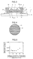
- FIG. 3 is a section A-A of the implementation structure of the semiconductor package illustrated in FIG. 1 .
- the semiconductor package 1 includes a wiring board 2, a semiconductor element 3, element electrodes 5, and side electrodes 7.
- the wiring board 2 having an outside shape of roughly a rectangular solid is internally wired by a not-shown conductive material, and is formed into a multi-layered structure.
- the wiring board 2 is mounted onto a motherboard 10 by soldering, and an element housing recessed portion 2a is formed in the surface (top surface) opposite of the mounting surface (bottom surface) to house the semiconductor element 3.
- the element housing recessed portion 2a is rectangle in shape extending in a planar direction.
- the "planar direction" is a direction parallel to the mounting surface of the package wiring board, as indicated in the direction of the XY plane in FIG. 1 .
- the semiconductor element 3 is adhered to a bottom surface 2a_ BASE of the element housing recessed portion 2a with an adhesive 6, and is electrically connected to the element electrodes 5 that are arranged on the bottom surface 2a_ BASE of the element housing recessed portion 2a by wires 4.
- the conductive material used in the internal wiring of the wiring board 2 and also the material of the element electrodes 5 are copper.
- the shapes of the wiring board 2 and the element housing recessed portion 2a are not limited to the ones described in the present embodiment.
- electrode recessed portions 2b are formed into semicircular columns extending from the bottom surface to the vicinity of the top surface.
- the electrode recessed portions 2b are designed to cut through the bottom surface of the wiring board 2 but not the top surface thereof.
- the electrode recessed portions 2b may be designed to cut through the bottom and top surfaces of the wiring board 2.
- side portions 7a of the side electrodes 7 do not always have to be arranged only on a pair of opposing outer side surfaces of the wiring board 2, but may be provided on all the outer side surfaces.
- the side electrode 7 includes a side portion 7a arranged on the each electrode recessed portion 2b of the wiring board 2 and a bottom portion 7b arranged on the bottom surface of the portion wiring board 2. Then, the side electrode 7 is combined with the wiring board 2 by coating the outer circumferential surface of the wiring board 2 with copper-nickel-gold plating. In this manner, because the side electrode 7 includes the bottom portion 7b, the side electrode 7 is prevented from coming off of the wiring board 2. In addition, the side electrode 7 is electrically connected to the element electrode 5 by way of the internal wiring of the wiring board 2.
- the motherboard 10 on which the semiconductor package 1 is mounted is a glass epoxy print wiring board.
- a plurality of motherboard electrodes 8 that are corresponding to the multiple side electrodes 7 are arranged.
- the semiconductor package 1 is electrically and mechanically connected to the motherboard 10 by soldering between these side electrodes 7 and the motherboard electrodes 8.
- Lead-free soldering is a preferable material of the solder 9, such as Sn-3Ag-0.5Cu and SnAg.
- the side electrode 7 and the motherboard electrode 8 are arranged such that the surface extending from the side portion 7a of the side electrode 7 (dotted line in FIG. 3 ) crosses the motherboard electrode 8.
- the two are positioned in such a manner that the two ends of the motherboard electrode 8 are laid across the surface extending from the side portion 7a of the side electrode 7, when viewed from the planar direction in FIG. 3 .
- the solder 9 is spread out and becomes solderable between the top surface of the motherboard electrode 8 and the bottom portion 7b and the side portion 7a of the side electrode 7 in soldering of the surface installation and in soldering with the laser, lamp, or hot-air heating method.
- the soldering state becomes easier to observe than in the arrangement of leads on the outer side surface of the package wiring board as in Patent Literature 1, while the mounting area of the semiconductor package 1 onto the motherboard 10 can be reduced.
- FIG. 4 is an enlarged sectional view of the wiring board 2 encircled by the dot-dash line in FIG. 3 .
- the wiring board 2 has a multilayered structure in which woven fabric 21 and a resin adhesive layer 22 are alternately laminated.
- the material of the woven fabric 21 should have a thermal expansion coefficient of approximately 1 ⁇ 10 -6 to 10 ⁇ 10 -6 l/K in the thickness direction (Z axis direction in FIG. 1 ), examples of which include resin woven fabric such as glass woven fabric and aramid woven fabric.
- an epoxy resin, a phenol resin, a polyimide resin may be adopted as the material of the resin adhesive of the resin adhesive layers 22.
- the thermal expansion coefficient in the planar direction can be matched to that of the motherboard that is a glass epoxy print wiring board.
- the element housing recessed portion 2a of the wiring board 2 is formed by preparing a wiring board in advance to have a multilayered structure in which the woven fabric 21 and the resin adhesive layer 22 are alternately laminated, and then cutting off the surface (top surface) opposite of the mounting surface (bottom surface). In this manner, the resin adhesive of the resin adhesive layers 22 is prevented from flowing into the inside of the element housing recessed portion 2a, which tends to occur when forming a recessed portion during the deposition of layers.
- the resin adhesive layer 22 include inorganic filler particles.
- any inorganic substance with a low thermal expansion coefficient can be adopted, examples of which include silica (SiO 2 ) particles and ceramic particles. Especially because of their low cost and ease of processing into a desired size, silica particles serve as the most suitable material.
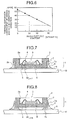
- FIG. 5 is a graph representing the relationship between the thermal expansion coefficient of the wiring board 2 in the direction of lamination and the equivalent plastic strain of the solder 9
- FIG. 6 is a graph representing the experimentally obtained relationship between the silica particle content in the resin adhesive layer 22 and the thermal expansion coefficient of the wiring board 2 in the direction of lamination.
- the plotted points of FIG. 5 represent values calculated by use of an analysis software program "ANSYS".
- ANSYS analysis software program
- the thermal expansion coefficients in the planar direction and Young's modulus of the solder 9 and the motherboard 10 were determined as shown in the table Table 1 Thermal expansion coefficient in planar direction Young's modulus solder 9 22 ⁇ 10 -6 1/K 32 GPa Motherboard 10 16 ⁇ 10 -6 1/K 24 GPa below.
- the "thermal expansion coefficient of the wiring board 2 in the direction of lamination" of FIG. 5 a desired value can be obtained by adjusting the silica particle content in accordance with the relationship indicated in FIG. 6 .
- the "equivalent plastic strain” in FIG. 5 means the plasticity of an equivalent strain from which the elasticity is excluded. As the value increases, cracks are more likely to occur in the soldered portion.
- the inventors of the present invention conducted a test of repeating the temperature cycle of 125 to -40 degrees Celsius, with the thermal expansion coefficient of the wiring board 2 in the direction of lamination being set approximately to 60 ⁇ 10 -6 l/K.
- glass woven fabric was used for the material of the woven fabric 21 of the wiring board 2
- an epoxy resin was used for the material of the resin adhesive of the resin adhesive layer 22
- the silica particle content in the resin adhesive layer 22 was set to 0 weight percent.
- the side electrode 7 was coated with copper-nickel-gold plating, Sn-3Ag-0.5Cu was adopted for the material of the solder 9, and a glass epoxy print wiring board was adopted for the motherboard 10.
- the inventors of the present invention have judged that a sufficient soldering reliability can be attained when the thermal expansion coefficient of the wiring board 2 in the direction of lamination is within a range of approximately 15 ⁇ 10 -6 to 40 ⁇ 10 -6 1/K.
- the silica particle content that is required when the thermal expansion coefficient of the wiring board 2 in the direction of lamination approximately should be set in the range of 15 ⁇ 10 -6 and 40 ⁇ 10 -6 1/K can be determined in accordance with the graph of FIG. 6 .
- the plotted points of FIG. 6 are experimental values. In this test, glass fabric was used for the material of the woven fabric 21 of the wiring board 2, an epoxy resin was used for the material of the resin adhesive of the resin adhesive layer 22, and silica particles were used for the material of the inorganic filler particles of the resin adhesive layer 22.
- the thermal expansion coefficient of the wiring board 2 in the direction of lamination can be set approximately to 15 ⁇ 10 -6 to 40 ⁇ 10 -6 1/K. Extrapolation was adopted to obtain the silica particle content of 80 weight percent for the thermal expansion coefficient of the wiring board 2 in the direction of lamination being approximately 15 ⁇ 10 -6 .
- a preferable range of the inorganic filler particle content is approximately between 30 and 80 weight percent.
- the side electrode 7 includes the bottom portion 7b, but it is sufficient that the side electrode 7 is provided at least with the side portion 7a.
- the semiconductor package 1 is mounted on the top surface of the motherboard 10 such that the end portions of the side electrodes 7 that extend to the bottom surface of the wiring board 2 are brought into contact with the motherboard electrodes 8, as illustrated in FIG. 7 .
- the solder 9 becomes spread and solderable between the side electrodes 7 of the semiconductor package 1 and the motherboard electrodes 8 of the motherboard 10.
- the woven fabric 21 of the wiring board 2, the resin adhesive of the resin adhesive layer 22, and the inorganic filler particles of the resin adhesive layer 22 each have layers that are formed of a single material to have the same content thereof, but different layers may have different materials as long as they can solve the problems of the present invention.
- the electrode recessed portions 2b are formed in the outer side surface of the wiring board 2, and the side portions 7a of the side electrodes 7 are arranged on the inner surfaces of the electrode recessed portions 2b, but as illustrated in FIG. 8 , flat side portions 7a of the side electrodes 7 may be provided without preparing any electrode recessed portions on the outer side surface of the wiring board 2.
- the resin adhesive layers 22 of the wiring board 2 contain inorganic filler particles, and thereby the thermal expansion coefficient of the wiring board 2 in the direction of lamination (z axis direction) can be adjusted. In this manner, strain that tends to appear in the solder 9 in the vicinity of the side portions 7a of the side electrodes 7 can be reduced. Hence, cracks can be prevented from occurring in the soldered portion in an environment in which rise and drop of temperature is repeated.
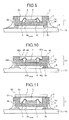
- FIG. 9 is a sectional view of the implementation structure of a semiconductor package according to the second embodiment of the present invention. Any portions the same as or equivalent to those of FIG. 3 are given the same numerals, and the explanation thereof is omitted here.
- the second to sixth embodiments are based essentially on the principles of the first embodiment.
- a side electrode 7 and a motherboard electrode 8 are arranged such that a surface extending from the side portion 7a of the side electrode 7 (dotted line in FIG. 9 ) crosses the motherboard electrode 8. Moreover, the two are arranged, as indicated by the dashed double-dotted lines in FIG. 9 , in such a manner that the inner end surface of the bottom portion 7b is positioned inside with respect to the inner end surface of the motherboard electrode 8 (toward the center of the wiring board 2).
- the size and the arrangement of the wiring board 2, the side electrode 7, or the motherboard electrode 8 are determined in such a manner that the distance between the inner end surfaces of the bottom portions 7b of the side electrodes 7 that face each other across the wiring board 2 is smaller than the distance between the inner end surfaces of the motherboard electrodes 8.
- solder 39 spreads out and becomes solderable between the top and inner end surfaces of the motherboard electrodes 8 and the bottom portions 7b and the side portions 7a of the side electrodes 7, and it extrudes into a convex shape toward the center of the wiring board 2 under a surface tension of the solder 39.
- the solder 39 spreads to the inner end surfaces of the motherboard electrodes 8 and becomes solderable there, and it extrudes into a convex shape toward the center of the wiring board 2 under the surface tension of the solder 39 so that the soldering area can be increased.
- the strain in the solder 39 can be reduced.
- cracks can be prevented from occurring in the soldered portion in an environment in which rise and fall of temperature are repeated.
- FIG. 10 is a sectional view of the implementation structure of a semiconductor package according to the third embodiment of the present invention. Any portions the same as or equivalent to those of FIG. 3 are given the same numerals, and the explanation thereof is omitted here.
- a semiconductor package 41 includes a wiring board 42, the semiconductor element 3, element electrodes 45, and the side electrodes 7.
- the wiring board 42 is internally wired by a not-shown conductive body, and it is formed by alternately laminating the woven fabric and resin adhesive layer that contains inorganic filler particles.
- the wiring board 42 includes an element housing recessed portion 42a in its top surface to house the semiconductor element 3, and it also includes multiple electrode recessed portions 42b on a pair of outer side surfaces that oppose each other to extend from the bottom surface to the vicinity of the top surface.
- a step portion 42c is formed on an inner side surface 42a_ SIDE of the element housing recessed portion 42a.
- the horizontal cross-sectional area of the element housing recessed portion 42a below the step portion 42c is smaller than the horizontal cross-sectional area above the step portion 42c.
- the semiconductor element 3 is fixed to a bottom surface 42a _BASE of the element housing recessed portion 42a with the adhesive 6, and the element electrode 45 is arranged on the top surface of the step portion 42c.
- the step portion 42c is provided approximately at the same height as the top surface of the semiconductor element 3. Then, the semiconductor element 3 and the element electrode 45 are electrically connected to each other by way of a wire 44, and the element electrode 45 and the side electrodes 7 are electrically connected to each other by the inner wiring of the wiring board 42.
- the step portion 42c on the inner side surface 42a _SIDE of the element housing recessed portion 42a, the cross-sectional area of the lower corner portion of the wiring board 42 in the planar direction can be increased.
- the wiring board 42 can be prevented from being deformed, and the strain in the solder 9 can be reduced.
- the step portion 42c approximately at the same height as the top surface of the semiconductor element 3, the length of the wire 44 that connects the semiconductor element 3 to the element electrode 45 can be reduced. In this manner, noise can be suppressed.
- FIG. 11 is a sectional view of the implementation structure of a semiconductor package according to the fourth embodiment of the present invention. Any portions the same as or equivalent to those of FIG. 3 are given the same numerals, and the explanation thereof is omitted here.
- a cover 50 is fixed onto the top surface of the wiring board 2 to cover the opening of the element housing recessed portion 2a.
- the cover 50 has a rectangular outer shape that is larger than the opening of the element housing recessed portion 2a, and is fixed by a fixing unit 51 that is arranged on the top surface of the wiring board 2 so that the entire opening of the element housing recessed portion 2a can be covered.
- the cover 50 serves to suppress the deformation of the top portion of the wiring board 2, and plastic or glass may be adopted as the material of the cover 50.
- a thermoset resin such as an epoxy resin, an ultraviolet curable resin, a thermoplastic resin, and solder may be adopted.
- the shape, area, and arrangement of the cover 50 are not limited to the above, as long as the deformation of the top portion of the wiring board 2 can be suppressed.
- it may be formed into a bar shape that has a width, when viewed from above, being greater than the width of the opening of the element housing recessed portion 2a and a length being smaller than the length of the element housing recessed portion 2a.
- shapes may be formed in the wiring board 2 and the cover 50 to be engaged with each other so that the cover 50 may be fixed directly to the wiring board 2, instead of fixing with the fixing unit 51.
- the cover 50 that is fixed onto the top surface of the wiring board 2 to partially or entirely cover the opening of the element housing recessed portion 2a, deformation of the top portion of the wiring board 2 can be suppressed, and the strain in the solder 9 can be reduced. Hence, cracks can be prevented from appearing in the soldered portion in an environment in which rise and fall of the temperature are repeated.
- the entire opening is covered to hermetically seal the element housing recessed portion 2a with the cover 50 so that dust is prevented from entering the element housing recessed portion 2a.
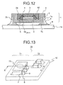
- FIG. 12 is a sectional view of the implementation structure of a semiconductor package according to the fifth embodiment of the present invention. Any portions the same as or equivalent to those of FIG. 3 are given the same numerals, and the explanation thereof is omitted here.
- the element housing recessed portion 2a of the wiring board 2 in which the semiconductor element 3 is housed is filled with a resin 60.
- the resin 60 serves to fix the wiring board 2 and suppress the deformation.
- silicon gel or silicon rubber may be adopted as the material of the resin 60.
- the resin 60 may be provided only in the vicinity of the boundary between the bottom surface 2a _BASE and an inner side surface 2a _SIDE of the element housing recessed portion 2a to suppress the deformation of the lower portion of the wiring board 2.
- the element housing recessed portion 2a is partially or entirely filled with the resin 60 so that the deformation of at least the lower portion of the wiring board 2 can be suppressed, and the strain in the solder 9 can be reduced. Hence, cracks can be prevented from occurring in the soldered portion in an environment in which rise and fall of temperature are repeated.
- the element housing recessed portion 2a is hermetically sealed with the resin 60, dust is prevented from entering the element housing recessed portion 2a.
- FIG. 13 is a perspective view of an optical semiconductor module according to the sixth embodiment of the present invention
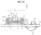
- FIG. 14 is a section B-B of the optical semiconductor module according to the sixth embodiment of the present invention. Any portions the same as or equivalent to those of FIG. 3 are given the same numerals, and the explanation thereof is omitted here.
- An optical semiconductor module 70 includes an optical semiconductor package 71 and multiple electronic parts 72 on the motherboard 10.
- the electronic parts 72 are mounted on the surface of the motherboard 10 on which the optical semiconductor package 71 is mounted and the other surface thereof by soldering.
- the optical semiconductor package 71 incorporates an emitting semiconductor element as the semiconductor element 3 of the semiconductor package 1, and a lens 73 is positioned on the top surface of the wiring board 2.
- the lens 73 includes a board portion 73a that has a horizontal cross-sectional area larger than the horizontal area of the opening of the element housing recessed portion 2a and is mounted on the top surface of the wiring board 2 so as to cover the opening of the element housing recessed portion 2a; and a convex portion 73b arranged at the position opposite of the semiconductor element 3 on a surface of the board portion 73a opposite of the surface that is in contact with the wiring board 2.
- the surface of the convex portion 73b that is in contact with the board portion 73a is circular and rises outward approximately in a hemisphere shape.
- the shape of the lens 73 is not limited thereto, however. The light emitted from the semiconductor element 3 passes through the lens 73 to the outside.
- the distance between the lens 73 and the semiconductor element 3 can be prevented from varying. Hence, a high-quality optical semiconductor module that has a stable light emission property can be achieved.
Landscapes
- Engineering & Computer Science (AREA)
- Manufacturing & Machinery (AREA)
- Microelectronics & Electronic Packaging (AREA)
- Structures Or Materials For Encapsulating Or Coating Semiconductor Devices Or Solid State Devices (AREA)
- Structures For Mounting Electric Components On Printed Circuit Boards (AREA)
- Electric Connection Of Electric Components To Printed Circuits (AREA)
- Production Of Multi-Layered Print Wiring Board (AREA)
Claims (9)
- Boîtier de semi-conducteur (1 ; 41) comprenant :une carte de câblage de boîtier (2 ; 42) qui a une portion évidée de logement d'élément (2a ; 42a) sur une surface supérieure de celle-ci pour loger un élément semi-conducteur (3) ;une pluralité d'électrodes latérales (7) qui sont agencées sur des surfaces latérales externes de la carte de câblage de boîtier (2 ; 42) et soudées à une pluralité d'électrodes de carte mère (8) agencées sur une carte mère (10) ;un élément semi-conducteur (3) qui est fixé sur une surface inférieure de la portion évidée de logement d'élément (2a ; 42a) ; etune électrode d'élément (5 ; 45) agencée sur la surface inférieure de la portion évidée de logement d'élément (2a ; 42a) et connectée électriquement à l'élément semi-conducteur (3) et aux électrodes latérales (7),la carte de câblage de boîtier (2 ; 42) a une structure multicouche dans laquelle un tissu tissé (21) et une couche adhésive de résine (22) sont stratifiées en alternance, une surface supérieure de la structure multicouche étant découpée pour former la portion évidée de logement d'élément (2a ; 42a) ;caractérisé en ce que :la carte de câblage de boîtier (2 ; i 42) est câblée intérieurement par un matériau conducteur pour connecter électriquement l'électrode latérale (7) et l'électrode d'élément (5, 45) ; etla couche adhésive de résine (22) est formée d'un adhésif de résine qui contient des particules de charge inorganiques ; etdans lequel, sur les surfaces latérales externes de la carte de câblage de boîtier (2 ; 42), des portions évidées d'électrodes (2b) sont conformées en colonnes semi-circulaires, conçues pour traverser une surface inférieure de la carte de câblage (2 ; 42), mais pas la surface supérieure de celle-ci, et des portions latérales (7a) des électrodes latérales (7) sont agencées sur chaque portion évidée (2b).
- Boîtier de semi-conducteur (41) selon la revendication 1, dans lequel une portion étagée (42c) est agencée sur une surface côté interne de la portion évidée de logement d'élément (42a) au même niveau qu'une surface supérieure de l'élément semi-conducteur (3), et l'électrode d'élément (45) est agencée sur une surface supérieure de la portion étagée (42c).
- Boîtier de semi-conducteur selon la revendication 1, comprenant en outre un couvercle (50) qui est fixé sur une surface supérieure de la carte de câblage de boîtier (2 ; 42) pour couvrir partiellement ou entièrement une ouverture de la portion évidée de logement d'élément (2a ; 42a).
- Boîtier de semi-conducteur selon la revendication 1, dans lequel la portion évidée de logement d'élément (2a ; 42a) est partiellement ou entièrement remplie de résine.
- Boîtier de semi-conducteur selon la revendication 1, dans lequel :la carte mère (10) est une carte de câblage imprimée de verre-époxyde ;la soudure (9 ; 39) est une soudure sans plomb ; etun coefficient de dilatation thermique de la carte de câblage de boîtier (2 ; 42) dans une direction de stratification est déterminé entre 15 x 10-6 et 40 x 10-6 1/K.
- Boîtier de semi-conducteur selon la revendication 1, dans lequel :la carte mère (10) est une carte de câblage imprimée de verre-époxyde ;la soudure (9 ; 39) est une soudure sans plomb ; etla teneur en particules de charge inorganiques de la couche adhésive de résine (22) est de 30 à 80 pour cent en poids.
- Structure d'application de boîtier de semi-conducteur, comprenant :le boîtier de semi-conducteur (1 ; 41) selon l'une quelconque des revendications 1 à 6 ;une carte mère (10) sur laquelle le boîtier de semi-conducteur (1 ; 41) est monté ;une pluralité d'électrodes de carte mère (8) qui sont agencées sur une surface de la carte mère (10) et fixées aux électrodes latérales (7) à l'aide d'une soudure (9 ; 39), dans laquelle :les électrodes latérales et les électrodes de carte mère (8) sont agencées d'une façon telle que les surfaces s'étendant des électrodes latérales (7) coupent les électrodes de carte mère (8) ; etla soudure (9 ; 39) est étalée et devient soudable entre les surfaces supérieures des électrodes de carte mère (8) et des électrodes latérales (7).
- Structure d'application de boîtier de semi-conducteur selon la revendication 7, dans laquelle :les électrodes latérales (7) sont chacune ménagées en formant d'un seul tenant une portion latérale (7a) agencée sur la surface latérale externe de la carte de câblage de boîtier (2 ; 42) et une portion inférieure (7b) agencée sur une surface inférieure de la carte de câblage de boîtier (2 ; 42) ;les électrodes latérales (7) et les électrodes de carte mère (8) sont agencées d'une façon telle que les surfaces s'étendant des portions latérales des électrodes latérales (7) coupent les électrodes de carte mère (8), et les surfaces d'extrémité internes des portions inférieures des électrodes latérales (7) sont positionnées à l'intérieur par rapport aux surfaces d'extrémité internes des électrodes de carte mère (8) ; etla soudure (9 ; 39) est étalée et devient soudable entre les surfaces supérieures et les surfaces d'extrémité internes des électrodes de carte mère (8) et des électrodes latérales (7).
- Structure d'application de boîtier de semi-conducteur selon la revendication 7, comprenant en outre une lentille (73) montée sur la surface supérieure de la carte de câblage de boîtier (2 ; 42),
dans laquelle l'élément semi-conducteur (3) est un élément semi-conducteur électroluminescent.
Applications Claiming Priority (1)
| Application Number | Priority Date | Filing Date | Title |
|---|---|---|---|
| PCT/JP2009/002813 WO2010150297A1 (fr) | 2009-06-22 | 2009-06-22 | Boîtier de semi-conducteur et structure de montage de boîtier de semi-conducteur |
Publications (3)
| Publication Number | Publication Date |
|---|---|
| EP2447989A1 EP2447989A1 (fr) | 2012-05-02 |
| EP2447989A4 EP2447989A4 (fr) | 2013-01-23 |
| EP2447989B1 true EP2447989B1 (fr) | 2016-05-04 |
Family
ID=43386098
Family Applications (1)
| Application Number | Title | Priority Date | Filing Date |
|---|---|---|---|
| EP09846434.0A Active EP2447989B1 (fr) | 2009-06-22 | 2009-06-22 | Boîtier de semi-conducteur et structure de montage de boîtier de semi-conducteur |
Country Status (6)
| Country | Link |
|---|---|
| US (1) | US20120091572A1 (fr) |
| EP (1) | EP2447989B1 (fr) |
| JP (1) | JP4823396B2 (fr) |
| KR (1) | KR101341273B1 (fr) |
| CN (1) | CN102460685B (fr) |
| WO (1) | WO2010150297A1 (fr) |
Families Citing this family (17)
| Publication number | Priority date | Publication date | Assignee | Title |
|---|---|---|---|---|
| JP6224473B2 (ja) * | 2014-02-03 | 2017-11-01 | 京セラ株式会社 | 配線基板、電子装置および電子モジュール |
| JP6166194B2 (ja) * | 2014-02-21 | 2017-07-19 | 京セラ株式会社 | 配線基板、電子装置および電子モジュール |
| US10863622B2 (en) * | 2017-05-05 | 2020-12-08 | Cyntec Co., Ltd. | Circuit board and electronic module with an electrode structure |
| KR102185706B1 (ko) * | 2017-11-08 | 2020-12-02 | 삼성전자주식회사 | 팬-아웃 반도체 패키지 |
| US10643919B2 (en) | 2017-11-08 | 2020-05-05 | Samsung Electronics Co., Ltd. | Fan-out semiconductor package |
| JP7049141B2 (ja) * | 2018-03-07 | 2022-04-06 | 新光電気工業株式会社 | 電子部品用パッケージとその製造方法 |
| JP7267767B2 (ja) * | 2019-02-20 | 2023-05-02 | ローム株式会社 | 半導体装置および半導体装置の製造方法 |
| EP3905315A4 (fr) | 2019-03-07 | 2022-10-19 | Absolics Inc. | Substrat d'emballage et appareil à semi-conducteur équipé dudit appareil |
| WO2020180149A1 (fr) | 2019-03-07 | 2020-09-10 | 에스케이씨 주식회사 | Substrat d'encapsulation et appareil à semi-conducteur le comportant |
| US11981501B2 (en) | 2019-03-12 | 2024-05-14 | Absolics Inc. | Loading cassette for substrate including glass and substrate loading method to which same is applied |
| US11652039B2 (en) | 2019-03-12 | 2023-05-16 | Absolics Inc. | Packaging substrate with core layer and cavity structure and semiconductor device comprising the same |
| US12198994B2 (en) | 2019-03-12 | 2025-01-14 | Absolics Inc. | Packaging substrate and method for manufacturing same |
| EP3916772A4 (fr) | 2019-03-12 | 2023-04-05 | Absolics Inc. | Substrat d'emballage et dispositif à semi-conducteur le comportant |
| CN114678344B (zh) | 2019-03-29 | 2025-08-15 | 爱玻索立克公司 | 半导体用封装玻璃基板、半导体封装基板及半导体装置 |
| ES2991528T3 (es) | 2019-08-23 | 2024-12-03 | Absolics Inc | Sustrato de embalaje y dispositivo semiconductor que comprende el mismo |
| WO2021079913A1 (fr) * | 2019-10-24 | 2021-04-29 | ローム株式会社 | Dispositif à semi-conducteur |
| EP4213197A1 (fr) * | 2022-01-12 | 2023-07-19 | Nexperia B.V. | Substrat d'emballage de semi-conducteur fabriqué à partir de matériau non métallique et son procédé de fabrication |
Citations (6)
| Publication number | Priority date | Publication date | Assignee | Title |
|---|---|---|---|---|
| JPS5954247A (ja) * | 1982-09-21 | 1984-03-29 | Nec Corp | 電子部品 |
| EP1050906A1 (fr) * | 1999-05-06 | 2000-11-08 | Murata Manufacturing Co., Ltd. | Boítier pour des composants électriques |
| US20020024130A1 (en) * | 1999-02-05 | 2002-02-28 | Satoshi Matsuo | Electronic component and electronic equipment using the same |
| US20070057364A1 (en) * | 2005-09-01 | 2007-03-15 | Wang Carl B | Low temperature co-fired ceramic (LTCC) tape compositions, light emitting diode (LED) modules, lighting devices and method of forming thereof |
| JP2007200997A (ja) * | 2006-01-24 | 2007-08-09 | Epson Toyocom Corp | 半田ペースト及び半田付け方法 |
| EP1876642A1 (fr) * | 2005-04-25 | 2008-01-09 | Sony Corporation | Carte de montage de composant électronique et dispositif électronique utilisant ladite carte |
Family Cites Families (21)
| Publication number | Priority date | Publication date | Assignee | Title |
|---|---|---|---|---|
| US4872825A (en) * | 1984-05-23 | 1989-10-10 | Ross Milton I | Method and apparatus for making encapsulated electronic circuit devices |
| US5677045A (en) * | 1993-09-14 | 1997-10-14 | Hitachi, Ltd. | Laminate and multilayer printed circuit board |
| JP3597913B2 (ja) * | 1995-07-20 | 2004-12-08 | 松下電器産業株式会社 | 半導体装置とその実装方法 |
| JPH11150211A (ja) * | 1997-11-18 | 1999-06-02 | Hitachi Cable Ltd | ハイブリッドicモジュール及びその製造方法 |
| JP3795248B2 (ja) * | 1999-03-19 | 2006-07-12 | ローム株式会社 | チップ型発光装置 |
| CN1195394C (zh) * | 1999-09-06 | 2005-03-30 | 铃木综业株式会社 | 线路板用基板 |
| TWI248842B (en) * | 2000-06-12 | 2006-02-11 | Hitachi Ltd | Semiconductor device and semiconductor module |
| JP4045781B2 (ja) * | 2001-08-28 | 2008-02-13 | 松下電工株式会社 | 発光装置 |
| JP4211359B2 (ja) * | 2002-03-06 | 2009-01-21 | 日亜化学工業株式会社 | 半導体装置の製造方法 |
| WO2005004195A2 (fr) * | 2003-07-03 | 2005-01-13 | Shellcase Ltd. | Procede et appareil d'encapsulation de circuits integres |
| JP2004140385A (ja) * | 2003-11-17 | 2004-05-13 | Kyocera Corp | 多層配線基板 |
| JP2005158770A (ja) * | 2003-11-20 | 2005-06-16 | Matsushita Electric Ind Co Ltd | 積層基板とその製造方法及び前記積層基板を用いたモジュールの製造方法とその製造装置 |
| JP4698259B2 (ja) * | 2005-03-16 | 2011-06-08 | 三洋電機株式会社 | 電子部品搭載用パッケージ及びパッケージ集合基板 |
| WO2006112474A2 (fr) * | 2005-04-19 | 2006-10-26 | Kaneka Corporation | Matériau composite fibre+résine, corps multicouche, carte de circuit imprimé, et procédé de fabrication de la carte de circuit imprimé |
| JP2007088155A (ja) * | 2005-09-21 | 2007-04-05 | Stanley Electric Co Ltd | 表面実装型led基板 |
| JPWO2007111236A1 (ja) * | 2006-03-24 | 2009-08-13 | イビデン株式会社 | 光電気配線板、光通信用デバイス及び光通信用デバイスの製造方法 |
| CN101536179B (zh) * | 2006-10-31 | 2011-05-25 | 皇家飞利浦电子股份有限公司 | 照明设备封装 |
| JP5048307B2 (ja) * | 2006-11-13 | 2012-10-17 | 信越石英株式会社 | 複合織物及びプリント配線基板 |
| US20090014746A1 (en) * | 2007-07-11 | 2009-01-15 | Ainissa Gweneth Ramirez | Solder alloys |
| JP5345363B2 (ja) * | 2008-06-24 | 2013-11-20 | シャープ株式会社 | 発光装置 |
| TWI381510B (zh) * | 2008-10-07 | 2013-01-01 | 日月光半導體製造股份有限公司 | 具有屏蔽蓋體之晶片封裝結構 |
-
2009
- 2009-06-22 EP EP09846434.0A patent/EP2447989B1/fr active Active
- 2009-06-22 KR KR1020117030645A patent/KR101341273B1/ko active Active
- 2009-06-22 WO PCT/JP2009/002813 patent/WO2010150297A1/fr not_active Ceased
- 2009-06-22 CN CN200980160025.5A patent/CN102460685B/zh active Active
- 2009-06-22 JP JP2011519300A patent/JP4823396B2/ja active Active
- 2009-06-22 US US13/379,930 patent/US20120091572A1/en not_active Abandoned
Patent Citations (6)
| Publication number | Priority date | Publication date | Assignee | Title |
|---|---|---|---|---|
| JPS5954247A (ja) * | 1982-09-21 | 1984-03-29 | Nec Corp | 電子部品 |
| US20020024130A1 (en) * | 1999-02-05 | 2002-02-28 | Satoshi Matsuo | Electronic component and electronic equipment using the same |
| EP1050906A1 (fr) * | 1999-05-06 | 2000-11-08 | Murata Manufacturing Co., Ltd. | Boítier pour des composants électriques |
| EP1876642A1 (fr) * | 2005-04-25 | 2008-01-09 | Sony Corporation | Carte de montage de composant électronique et dispositif électronique utilisant ladite carte |
| US20070057364A1 (en) * | 2005-09-01 | 2007-03-15 | Wang Carl B | Low temperature co-fired ceramic (LTCC) tape compositions, light emitting diode (LED) modules, lighting devices and method of forming thereof |
| JP2007200997A (ja) * | 2006-01-24 | 2007-08-09 | Epson Toyocom Corp | 半田ペースト及び半田付け方法 |
Also Published As
| Publication number | Publication date |
|---|---|
| EP2447989A1 (fr) | 2012-05-02 |
| CN102460685A (zh) | 2012-05-16 |
| CN102460685B (zh) | 2014-08-06 |
| KR20120023120A (ko) | 2012-03-12 |
| US20120091572A1 (en) | 2012-04-19 |
| HK1167740A1 (en) | 2012-12-07 |
| WO2010150297A1 (fr) | 2010-12-29 |
| KR101341273B1 (ko) | 2013-12-12 |
| EP2447989A4 (fr) | 2013-01-23 |
| JP4823396B2 (ja) | 2011-11-24 |
| JPWO2010150297A1 (ja) | 2012-12-06 |
Similar Documents
| Publication | Publication Date | Title |
|---|---|---|
| EP2447989B1 (fr) | Boîtier de semi-conducteur et structure de montage de boîtier de semi-conducteur | |
| US8168453B2 (en) | Light emitting diode package and fabrication method thereof | |
| US7450395B2 (en) | Circuit module and circuit device including circuit module | |
| JPH01199497A (ja) | 電子部品塔載用基板 | |
| US10580711B2 (en) | Electronic device mounting board and electronic package | |
| US20140028155A1 (en) | Electronic component and manufacturing method for the electronic component | |
| CN1581482A (zh) | 电路模块 | |
| JP5207278B2 (ja) | 保護回路モジュール | |
| JP2002217514A (ja) | マルチチップ半導体装置 | |
| CN100345290C (zh) | 半导体器件 | |
| US8422241B2 (en) | Sealed electronic control device and method of fabricating the same | |
| US20130140664A1 (en) | Flip chip packaging structure | |
| KR101331737B1 (ko) | 반도체 패키지 | |
| US8736044B2 (en) | Lid for an electrical hardware component | |
| KR20140063713A (ko) | 몰딩된 하우징을 구비한 전기 제어 장치 | |
| US20050280018A1 (en) | Light-emitting diode | |
| CN1139984C (zh) | 半导体装置、装配方法、电路基板和柔软基板及制造方法 | |
| US20110068451A1 (en) | Multi-chip semiconductor connector | |
| KR101675008B1 (ko) | 광전자 모듈 그리고 광전자 모듈을 제조하기 위한 방법 | |
| JPH056989A (ja) | 撮像装置およびその製造方法 | |
| JPH1051034A (ja) | 面実装型電子部品、その製造方法、これを回路基板上に実装する方法、およびこれを実装した回路基板 | |
| US20090146275A1 (en) | Lead frame and semiconductor device provided with lead frame | |
| CN1591863A (zh) | 半导体器件、半导体组件及半导体器件的制造方法 | |
| WO2011108051A1 (fr) | Dispositif à semi-conducteurs | |
| HK1167740B (en) | Semiconductor package and semiconductor package mounting structure |
Legal Events
| Date | Code | Title | Description |
|---|---|---|---|
| PUAI | Public reference made under article 153(3) epc to a published international application that has entered the european phase |
Free format text: ORIGINAL CODE: 0009012 |
|
| 17P | Request for examination filed |
Effective date: 20111221 |
|
| AK | Designated contracting states |
Kind code of ref document: A1 Designated state(s): AT BE BG CH CY CZ DE DK EE ES FI FR GB GR HR HU IE IS IT LI LT LU LV MC MK MT NL NO PL PT RO SE SI SK TR |
|
| DAX | Request for extension of the european patent (deleted) | ||
| A4 | Supplementary search report drawn up and despatched |
Effective date: 20121221 |
|
| RIC1 | Information provided on ipc code assigned before grant |
Ipc: H01L 23/055 20060101ALI20121217BHEP Ipc: H05K 1/18 20060101ALI20121217BHEP Ipc: H01L 23/13 20060101ALI20121217BHEP Ipc: H01L 23/14 20060101ALI20121217BHEP Ipc: H05K 1/03 20060101ALI20121217BHEP Ipc: H01L 23/28 20060101ALI20121217BHEP Ipc: H01L 23/08 20060101ALI20121217BHEP Ipc: H01L 23/24 20060101ALI20121217BHEP Ipc: H01L 23/12 20060101AFI20121217BHEP Ipc: H01L 23/498 20060101ALI20121217BHEP Ipc: H05K 3/34 20060101ALI20121217BHEP |
|
| 17Q | First examination report despatched |
Effective date: 20130808 |
|
| REG | Reference to a national code |
Ref country code: DE Ref legal event code: R079 Ref document number: 602009038525 Country of ref document: DE Free format text: PREVIOUS MAIN CLASS: H01L0023120000 Ipc: H01L0023000000 |
|
| GRAP | Despatch of communication of intention to grant a patent |
Free format text: ORIGINAL CODE: EPIDOSNIGR1 |
|
| RIC1 | Information provided on ipc code assigned before grant |
Ipc: H01L 23/13 20060101ALI20151028BHEP Ipc: H05K 3/34 20060101ALI20151028BHEP Ipc: H01L 23/055 20060101ALI20151028BHEP Ipc: H01L 23/24 20060101ALI20151028BHEP Ipc: H01L 23/00 20060101AFI20151028BHEP Ipc: H01L 23/498 20060101ALI20151028BHEP Ipc: H01L 23/14 20060101ALI20151028BHEP |
|
| INTG | Intention to grant announced |
Effective date: 20151118 |
|
| GRAS | Grant fee paid |
Free format text: ORIGINAL CODE: EPIDOSNIGR3 |
|
| GRAA | (expected) grant |
Free format text: ORIGINAL CODE: 0009210 |
|
| AK | Designated contracting states |
Kind code of ref document: B1 Designated state(s): AT BE BG CH CY CZ DE DK EE ES FI FR GB GR HR HU IE IS IT LI LT LU LV MC MK MT NL NO PL PT RO SE SI SK TR |
|
| REG | Reference to a national code |
Ref country code: GB Ref legal event code: FG4D |
|
| REG | Reference to a national code |
Ref country code: CH Ref legal event code: EP |
|
| REG | Reference to a national code |
Ref country code: AT Ref legal event code: REF Ref document number: 797577 Country of ref document: AT Kind code of ref document: T Effective date: 20160515 |
|
| REG | Reference to a national code |
Ref country code: IE Ref legal event code: FG4D |
|
| REG | Reference to a national code |
Ref country code: DE Ref legal event code: R096 Ref document number: 602009038525 Country of ref document: DE |
|
| REG | Reference to a national code |
Ref country code: NL Ref legal event code: MP Effective date: 20160504 |
|
| REG | Reference to a national code |
Ref country code: LT Ref legal event code: MG4D |
|
| PG25 | Lapsed in a contracting state [announced via postgrant information from national office to epo] |
Ref country code: NO Free format text: LAPSE BECAUSE OF FAILURE TO SUBMIT A TRANSLATION OF THE DESCRIPTION OR TO PAY THE FEE WITHIN THE PRESCRIBED TIME-LIMIT Effective date: 20160804 Ref country code: LT Free format text: LAPSE BECAUSE OF FAILURE TO SUBMIT A TRANSLATION OF THE DESCRIPTION OR TO PAY THE FEE WITHIN THE PRESCRIBED TIME-LIMIT Effective date: 20160504 Ref country code: FI Free format text: LAPSE BECAUSE OF FAILURE TO SUBMIT A TRANSLATION OF THE DESCRIPTION OR TO PAY THE FEE WITHIN THE PRESCRIBED TIME-LIMIT Effective date: 20160504 Ref country code: NL Free format text: LAPSE BECAUSE OF FAILURE TO SUBMIT A TRANSLATION OF THE DESCRIPTION OR TO PAY THE FEE WITHIN THE PRESCRIBED TIME-LIMIT Effective date: 20160504 |
|
| REG | Reference to a national code |
Ref country code: AT Ref legal event code: MK05 Ref document number: 797577 Country of ref document: AT Kind code of ref document: T Effective date: 20160504 |
|
| PG25 | Lapsed in a contracting state [announced via postgrant information from national office to epo] |
Ref country code: LV Free format text: LAPSE BECAUSE OF FAILURE TO SUBMIT A TRANSLATION OF THE DESCRIPTION OR TO PAY THE FEE WITHIN THE PRESCRIBED TIME-LIMIT Effective date: 20160504 Ref country code: SE Free format text: LAPSE BECAUSE OF FAILURE TO SUBMIT A TRANSLATION OF THE DESCRIPTION OR TO PAY THE FEE WITHIN THE PRESCRIBED TIME-LIMIT Effective date: 20160504 Ref country code: ES Free format text: LAPSE BECAUSE OF FAILURE TO SUBMIT A TRANSLATION OF THE DESCRIPTION OR TO PAY THE FEE WITHIN THE PRESCRIBED TIME-LIMIT Effective date: 20160504 Ref country code: GR Free format text: LAPSE BECAUSE OF FAILURE TO SUBMIT A TRANSLATION OF THE DESCRIPTION OR TO PAY THE FEE WITHIN THE PRESCRIBED TIME-LIMIT Effective date: 20160805 Ref country code: HR Free format text: LAPSE BECAUSE OF FAILURE TO SUBMIT A TRANSLATION OF THE DESCRIPTION OR TO PAY THE FEE WITHIN THE PRESCRIBED TIME-LIMIT Effective date: 20160504 Ref country code: PT Free format text: LAPSE BECAUSE OF FAILURE TO SUBMIT A TRANSLATION OF THE DESCRIPTION OR TO PAY THE FEE WITHIN THE PRESCRIBED TIME-LIMIT Effective date: 20160905 |
|
| PG25 | Lapsed in a contracting state [announced via postgrant information from national office to epo] |
Ref country code: BE Free format text: LAPSE BECAUSE OF NON-PAYMENT OF DUE FEES Effective date: 20160630 Ref country code: IT Free format text: LAPSE BECAUSE OF FAILURE TO SUBMIT A TRANSLATION OF THE DESCRIPTION OR TO PAY THE FEE WITHIN THE PRESCRIBED TIME-LIMIT Effective date: 20160504 |
|
| PG25 | Lapsed in a contracting state [announced via postgrant information from national office to epo] |
Ref country code: SK Free format text: LAPSE BECAUSE OF FAILURE TO SUBMIT A TRANSLATION OF THE DESCRIPTION OR TO PAY THE FEE WITHIN THE PRESCRIBED TIME-LIMIT Effective date: 20160504 Ref country code: DK Free format text: LAPSE BECAUSE OF FAILURE TO SUBMIT A TRANSLATION OF THE DESCRIPTION OR TO PAY THE FEE WITHIN THE PRESCRIBED TIME-LIMIT Effective date: 20160504 Ref country code: CZ Free format text: LAPSE BECAUSE OF FAILURE TO SUBMIT A TRANSLATION OF THE DESCRIPTION OR TO PAY THE FEE WITHIN THE PRESCRIBED TIME-LIMIT Effective date: 20160504 Ref country code: EE Free format text: LAPSE BECAUSE OF FAILURE TO SUBMIT A TRANSLATION OF THE DESCRIPTION OR TO PAY THE FEE WITHIN THE PRESCRIBED TIME-LIMIT Effective date: 20160504 Ref country code: RO Free format text: LAPSE BECAUSE OF FAILURE TO SUBMIT A TRANSLATION OF THE DESCRIPTION OR TO PAY THE FEE WITHIN THE PRESCRIBED TIME-LIMIT Effective date: 20160504 |
|
| REG | Reference to a national code |
Ref country code: CH Ref legal event code: PL |
|
| REG | Reference to a national code |
Ref country code: DE Ref legal event code: R097 Ref document number: 602009038525 Country of ref document: DE |
|
| PG25 | Lapsed in a contracting state [announced via postgrant information from national office to epo] |
Ref country code: AT Free format text: LAPSE BECAUSE OF FAILURE TO SUBMIT A TRANSLATION OF THE DESCRIPTION OR TO PAY THE FEE WITHIN THE PRESCRIBED TIME-LIMIT Effective date: 20160504 Ref country code: BE Free format text: LAPSE BECAUSE OF FAILURE TO SUBMIT A TRANSLATION OF THE DESCRIPTION OR TO PAY THE FEE WITHIN THE PRESCRIBED TIME-LIMIT Effective date: 20160504 Ref country code: PL Free format text: LAPSE BECAUSE OF FAILURE TO SUBMIT A TRANSLATION OF THE DESCRIPTION OR TO PAY THE FEE WITHIN THE PRESCRIBED TIME-LIMIT Effective date: 20160504 |
|
| PLBE | No opposition filed within time limit |
Free format text: ORIGINAL CODE: 0009261 |
|
| STAA | Information on the status of an ep patent application or granted ep patent |
Free format text: STATUS: NO OPPOSITION FILED WITHIN TIME LIMIT |
|
| REG | Reference to a national code |
Ref country code: IE Ref legal event code: MM4A |
|
| PG25 | Lapsed in a contracting state [announced via postgrant information from national office to epo] |
Ref country code: MC Free format text: LAPSE BECAUSE OF FAILURE TO SUBMIT A TRANSLATION OF THE DESCRIPTION OR TO PAY THE FEE WITHIN THE PRESCRIBED TIME-LIMIT Effective date: 20160504 |
|
| REG | Reference to a national code |
Ref country code: FR Ref legal event code: ST Effective date: 20170228 |
|
| 26N | No opposition filed |
Effective date: 20170207 |
|
| PG25 | Lapsed in a contracting state [announced via postgrant information from national office to epo] |
Ref country code: CH Free format text: LAPSE BECAUSE OF NON-PAYMENT OF DUE FEES Effective date: 20160630 Ref country code: LI Free format text: LAPSE BECAUSE OF NON-PAYMENT OF DUE FEES Effective date: 20160630 Ref country code: FR Free format text: LAPSE BECAUSE OF NON-PAYMENT OF DUE FEES Effective date: 20160704 |
|
| PG25 | Lapsed in a contracting state [announced via postgrant information from national office to epo] |
Ref country code: SI Free format text: LAPSE BECAUSE OF FAILURE TO SUBMIT A TRANSLATION OF THE DESCRIPTION OR TO PAY THE FEE WITHIN THE PRESCRIBED TIME-LIMIT Effective date: 20160504 Ref country code: IE Free format text: LAPSE BECAUSE OF NON-PAYMENT OF DUE FEES Effective date: 20160622 |
|
| REG | Reference to a national code |
Ref country code: DE Ref legal event code: R084 Ref document number: 602009038525 Country of ref document: DE |
|
| REG | Reference to a national code |
Ref country code: GB Ref legal event code: 746 Effective date: 20180206 |
|
| PG25 | Lapsed in a contracting state [announced via postgrant information from national office to epo] |
Ref country code: HU Free format text: LAPSE BECAUSE OF FAILURE TO SUBMIT A TRANSLATION OF THE DESCRIPTION OR TO PAY THE FEE WITHIN THE PRESCRIBED TIME-LIMIT; INVALID AB INITIO Effective date: 20090622 Ref country code: CY Free format text: LAPSE BECAUSE OF FAILURE TO SUBMIT A TRANSLATION OF THE DESCRIPTION OR TO PAY THE FEE WITHIN THE PRESCRIBED TIME-LIMIT Effective date: 20160504 |
|
| PG25 | Lapsed in a contracting state [announced via postgrant information from national office to epo] |
Ref country code: TR Free format text: LAPSE BECAUSE OF FAILURE TO SUBMIT A TRANSLATION OF THE DESCRIPTION OR TO PAY THE FEE WITHIN THE PRESCRIBED TIME-LIMIT Effective date: 20160504 Ref country code: LU Free format text: LAPSE BECAUSE OF NON-PAYMENT OF DUE FEES Effective date: 20160622 Ref country code: IS Free format text: LAPSE BECAUSE OF FAILURE TO SUBMIT A TRANSLATION OF THE DESCRIPTION OR TO PAY THE FEE WITHIN THE PRESCRIBED TIME-LIMIT Effective date: 20160504 Ref country code: MK Free format text: LAPSE BECAUSE OF FAILURE TO SUBMIT A TRANSLATION OF THE DESCRIPTION OR TO PAY THE FEE WITHIN THE PRESCRIBED TIME-LIMIT Effective date: 20160504 Ref country code: MT Free format text: LAPSE BECAUSE OF NON-PAYMENT OF DUE FEES Effective date: 20160630 |
|
| PG25 | Lapsed in a contracting state [announced via postgrant information from national office to epo] |
Ref country code: BG Free format text: LAPSE BECAUSE OF FAILURE TO SUBMIT A TRANSLATION OF THE DESCRIPTION OR TO PAY THE FEE WITHIN THE PRESCRIBED TIME-LIMIT Effective date: 20160504 |
|
| P01 | Opt-out of the competence of the unified patent court (upc) registered |
Effective date: 20230512 |
|
| PGFP | Annual fee paid to national office [announced via postgrant information from national office to epo] |
Ref country code: DE Payment date: 20250429 Year of fee payment: 17 |
|
| PGFP | Annual fee paid to national office [announced via postgrant information from national office to epo] |
Ref country code: GB Payment date: 20250501 Year of fee payment: 17 |
|
| REG | Reference to a national code |
Ref country code: DE Ref legal event code: R079 Ref document number: 602009038525 Country of ref document: DE Free format text: PREVIOUS MAIN CLASS: H01L0023000000 Ipc: H10W0099000000 |