EP2455966A1 - Dispositif electroluminescent - Google Patents
Dispositif electroluminescent Download PDFInfo
- Publication number
- EP2455966A1 EP2455966A1 EP10799683A EP10799683A EP2455966A1 EP 2455966 A1 EP2455966 A1 EP 2455966A1 EP 10799683 A EP10799683 A EP 10799683A EP 10799683 A EP10799683 A EP 10799683A EP 2455966 A1 EP2455966 A1 EP 2455966A1
- Authority
- EP
- European Patent Office
- Prior art keywords
- electrode
- substrate electrode
- substrate
- light emitting
- outer periphery
- Prior art date
- Legal status (The legal status is an assumption and is not a legal conclusion. Google has not performed a legal analysis and makes no representation as to the accuracy of the status listed.)
- Granted
Links
Images





Classifications
-
- H—ELECTRICITY
- H10—SEMICONDUCTOR DEVICES; ELECTRIC SOLID-STATE DEVICES NOT OTHERWISE PROVIDED FOR
- H10H—INORGANIC LIGHT-EMITTING SEMICONDUCTOR DEVICES HAVING POTENTIAL BARRIERS
- H10H20/00—Individual inorganic light-emitting semiconductor devices having potential barriers, e.g. light-emitting diodes [LED]
- H10H20/80—Constructional details
- H10H20/83—Electrodes
- H10H20/831—Electrodes characterised by their shape
-
- H—ELECTRICITY
- H10—SEMICONDUCTOR DEVICES; ELECTRIC SOLID-STATE DEVICES NOT OTHERWISE PROVIDED FOR
- H10H—INORGANIC LIGHT-EMITTING SEMICONDUCTOR DEVICES HAVING POTENTIAL BARRIERS
- H10H20/00—Individual inorganic light-emitting semiconductor devices having potential barriers, e.g. light-emitting diodes [LED]
- H10H20/80—Constructional details
- H10H20/85—Packages
-
- H—ELECTRICITY
- H10—SEMICONDUCTOR DEVICES; ELECTRIC SOLID-STATE DEVICES NOT OTHERWISE PROVIDED FOR
- H10W—GENERIC PACKAGES, INTERCONNECTIONS, CONNECTORS OR OTHER CONSTRUCTIONAL DETAILS OF DEVICES COVERED BY CLASS H10
- H10W70/00—Package substrates; Interposers; Redistribution layers [RDL]
- H10W70/60—Insulating or insulated package substrates; Interposers; Redistribution layers
-
- H—ELECTRICITY
- H10—SEMICONDUCTOR DEVICES; ELECTRIC SOLID-STATE DEVICES NOT OTHERWISE PROVIDED FOR
- H10H—INORGANIC LIGHT-EMITTING SEMICONDUCTOR DEVICES HAVING POTENTIAL BARRIERS
- H10H20/00—Individual inorganic light-emitting semiconductor devices having potential barriers, e.g. light-emitting diodes [LED]
- H10H20/80—Constructional details
- H10H20/85—Packages
- H10H20/857—Interconnections, e.g. lead-frames, bond wires or solder balls
-
- H—ELECTRICITY
- H10—SEMICONDUCTOR DEVICES; ELECTRIC SOLID-STATE DEVICES NOT OTHERWISE PROVIDED FOR
- H10W—GENERIC PACKAGES, INTERCONNECTIONS, CONNECTORS OR OTHER CONSTRUCTIONAL DETAILS OF DEVICES COVERED BY CLASS H10
- H10W72/00—Interconnections or connectors in packages
- H10W72/071—Connecting or disconnecting
- H10W72/072—Connecting or disconnecting of bump connectors
- H10W72/07251—Connecting or disconnecting of bump connectors characterised by changes in properties of the bump connectors during connecting
-
- H—ELECTRICITY
- H10—SEMICONDUCTOR DEVICES; ELECTRIC SOLID-STATE DEVICES NOT OTHERWISE PROVIDED FOR
- H10W—GENERIC PACKAGES, INTERCONNECTIONS, CONNECTORS OR OTHER CONSTRUCTIONAL DETAILS OF DEVICES COVERED BY CLASS H10
- H10W72/00—Interconnections or connectors in packages
- H10W72/071—Connecting or disconnecting
- H10W72/073—Connecting or disconnecting of die-attach connectors
-
- H—ELECTRICITY
- H10—SEMICONDUCTOR DEVICES; ELECTRIC SOLID-STATE DEVICES NOT OTHERWISE PROVIDED FOR
- H10W—GENERIC PACKAGES, INTERCONNECTIONS, CONNECTORS OR OTHER CONSTRUCTIONAL DETAILS OF DEVICES COVERED BY CLASS H10
- H10W72/00—Interconnections or connectors in packages
- H10W72/071—Connecting or disconnecting
- H10W72/073—Connecting or disconnecting of die-attach connectors
- H10W72/07331—Connecting techniques
- H10W72/07336—Soldering or alloying
-
- H—ELECTRICITY
- H10—SEMICONDUCTOR DEVICES; ELECTRIC SOLID-STATE DEVICES NOT OTHERWISE PROVIDED FOR
- H10W—GENERIC PACKAGES, INTERCONNECTIONS, CONNECTORS OR OTHER CONSTRUCTIONAL DETAILS OF DEVICES COVERED BY CLASS H10
- H10W72/00—Interconnections or connectors in packages
- H10W72/20—Bump connectors, e.g. solder bumps or copper pillars; Dummy bumps; Thermal bumps
-
- H—ELECTRICITY
- H10—SEMICONDUCTOR DEVICES; ELECTRIC SOLID-STATE DEVICES NOT OTHERWISE PROVIDED FOR
- H10W—GENERIC PACKAGES, INTERCONNECTIONS, CONNECTORS OR OTHER CONSTRUCTIONAL DETAILS OF DEVICES COVERED BY CLASS H10
- H10W72/00—Interconnections or connectors in packages
- H10W72/20—Bump connectors, e.g. solder bumps or copper pillars; Dummy bumps; Thermal bumps
- H10W72/29—Bond pads specially adapted therefor
-
- H—ELECTRICITY
- H10—SEMICONDUCTOR DEVICES; ELECTRIC SOLID-STATE DEVICES NOT OTHERWISE PROVIDED FOR
- H10W—GENERIC PACKAGES, INTERCONNECTIONS, CONNECTORS OR OTHER CONSTRUCTIONAL DETAILS OF DEVICES COVERED BY CLASS H10
- H10W72/00—Interconnections or connectors in packages
- H10W72/30—Die-attach connectors
-
- H—ELECTRICITY
- H10—SEMICONDUCTOR DEVICES; ELECTRIC SOLID-STATE DEVICES NOT OTHERWISE PROVIDED FOR
- H10W—GENERIC PACKAGES, INTERCONNECTIONS, CONNECTORS OR OTHER CONSTRUCTIONAL DETAILS OF DEVICES COVERED BY CLASS H10
- H10W72/00—Interconnections or connectors in packages
- H10W72/50—Bond wires
- H10W72/59—Bond pads specially adapted therefor
-
- H—ELECTRICITY
- H10—SEMICONDUCTOR DEVICES; ELECTRIC SOLID-STATE DEVICES NOT OTHERWISE PROVIDED FOR
- H10W—GENERIC PACKAGES, INTERCONNECTIONS, CONNECTORS OR OTHER CONSTRUCTIONAL DETAILS OF DEVICES COVERED BY CLASS H10
- H10W72/00—Interconnections or connectors in packages
- H10W72/90—Bond pads, in general
- H10W72/931—Shapes of bond pads
- H10W72/932—Plan-view shape, i.e. in top view
-
- H—ELECTRICITY
- H10—SEMICONDUCTOR DEVICES; ELECTRIC SOLID-STATE DEVICES NOT OTHERWISE PROVIDED FOR
- H10W—GENERIC PACKAGES, INTERCONNECTIONS, CONNECTORS OR OTHER CONSTRUCTIONAL DETAILS OF DEVICES COVERED BY CLASS H10
- H10W72/00—Interconnections or connectors in packages
- H10W72/90—Bond pads, in general
- H10W72/931—Shapes of bond pads
- H10W72/936—Multiple bond pads having different shapes
-
- H—ELECTRICITY
- H10—SEMICONDUCTOR DEVICES; ELECTRIC SOLID-STATE DEVICES NOT OTHERWISE PROVIDED FOR
- H10W—GENERIC PACKAGES, INTERCONNECTIONS, CONNECTORS OR OTHER CONSTRUCTIONAL DETAILS OF DEVICES COVERED BY CLASS H10
- H10W72/00—Interconnections or connectors in packages
- H10W72/90—Bond pads, in general
- H10W72/941—Dispositions of bond pads
-
- H—ELECTRICITY
- H10—SEMICONDUCTOR DEVICES; ELECTRIC SOLID-STATE DEVICES NOT OTHERWISE PROVIDED FOR
- H10W—GENERIC PACKAGES, INTERCONNECTIONS, CONNECTORS OR OTHER CONSTRUCTIONAL DETAILS OF DEVICES COVERED BY CLASS H10
- H10W72/00—Interconnections or connectors in packages
- H10W72/90—Bond pads, in general
- H10W72/951—Materials of bond pads
-
- H—ELECTRICITY
- H10—SEMICONDUCTOR DEVICES; ELECTRIC SOLID-STATE DEVICES NOT OTHERWISE PROVIDED FOR
- H10W—GENERIC PACKAGES, INTERCONNECTIONS, CONNECTORS OR OTHER CONSTRUCTIONAL DETAILS OF DEVICES COVERED BY CLASS H10
- H10W90/00—Package configurations
- H10W90/701—Package configurations characterised by the relative positions of pads or connectors relative to package parts
- H10W90/731—Package configurations characterised by the relative positions of pads or connectors relative to package parts of die-attach connectors
- H10W90/734—Package configurations characterised by the relative positions of pads or connectors relative to package parts of die-attach connectors between a chip and a stacked insulating package substrate, interposer or RDL
Definitions
- the present invention relates to a light emitting device, in which elements such as light emitting elements are mounted on a mounting substrate such as a semiconductor insulating substrate.
- a surface-mounting type light emitting device with a light emitting element such as a light emission diode (LED) or a laser diode (LD) mounted on a substrate is conventionally well known.
- the light-emitting device has been used in lighting equipment, a backlight for display screen, an automotive illuminant, a display illuminant, and an auxiliary illuminant for motion pictures, as well as for other general consumer illuminants.
- a device with a configuration comprising both anodes and cathodes mounted on the same surface is widely used in order to enhance its light extraction efficiency.
- a widely proposed light-emitting device has a configuration comprising chips mounted, by a flip-chip method, on an insulating substrate, on which wiring patterns are formed.
- One example of the light emitting device is manufactured by applying a solder paste at specific positions on a pair of electrodes formed on a insulating substrate, mounting LED elements by flip-chip mounting in order to bond the LED elements, and melting the solder paste by reflowing in order to make the electrodes and the LED elements electrically connected to each other. If the pair of the electrodes formed on the insulating substrate of the light emitting device are formed into a shape identical to that of the electrodes on the side of the LED elements, when the LED elements are mounted by pressing themselves against the electrodes, a portion of the solder paste applied on the insulating substrate bulges out around the electrode, comes off the electrodes during the reflowing process, and forms a solder ball.
- patent document 1 discloses a configuration for preventing solder ball generation by providing a redundant reflow pad along the outer circumference of the LED element.
- patent document 2 discloses another configuration which ensures self-alignment by setting a length and a width of a rectangular die pad at 0.5-1.5 times of those of the rectangular light emitting diode of the light emitting device.
- Patent document 2 also discloses a configuration in which extended sections extending from each of the four sides of the light emitting diode are provided when a light emitting diode is mounted on the die pad at the side of the insulating substrate. The extended sections are able to lower the height of the molten solder deposited on the surface of the die pad so that self alignment by the surface tension of the molten soldier is ensured.
- the configuration of the light emitting device of patent document 2 may enable self-alignment during the reflowing process
- the mechanism of self-alignment assumes the shape of the die pad as a single unit. Therefore, when the device comprises separate die pads for one element such as a light emitting diode, in other words, when the configuration of the device comprises multiple electrodes on the side of a substrate, such as a first substrate electrode and a second substrate electrode mounted at separate positions on the substrate, the configuration is unsatisfactory for performing self-alignment while preventing the solder ball generation.
- the electrodes formed on the substrate are a first electrode and a second electrode, corresponding to a P-type electrode and a N-type electrode, and are separated from each other, the molten solder may converge towards the second electrode from the first electrode. Therefore, the converging molten solder forms an excessive connecting thickness of the second electrode, and may lift up some portion of the molten solder around the first electrode, generating voids in the molten solder near the first electrode. Therefore, a method for prevention of the voids around the first electrode in a light emitting device is desired.
- the objective of the present invention made in view of the above-mentioned problems is to provide a light emitting device that secures self-alignment, and prevents the generation of solder balls as well as the generation of voids in molten solder under the electrodes, even in case of electrodes formed separately from each other on a substrate having a single mounted element.
- the light emitting device of claim 1 has a configuration, in which a light emitting device comprises: a substrate including a first substrate electrode and a second electrode, both of which are formed on the substrate; and an element in a rectangular shape, the element including a first element electrode and a second element electrode, which are formed inside an outer periphery of the element and aligned respectively with the first substrate electrode and the second substrate electrode via a heat-melted connecting material, wherein: each of the first substrate electrode and the second substrate electrode is formed into a shape which is identical with at least a portion of an outer periphery of one of the first element electrode and the second element electrode, which is aligned with the each of the first substrate electrode and the second substrate electrode; the first substrate electrode is provided with a recessed concave portion, which is formed by cutting off a portion on the outer periphery of the first substrate electrode; the second substrate electrode is formed along and off the recessed concave portion of the first substrate electrode; each of the first substrate electrode and the
- the light emitting device comprises the first substrate electrode and the second substrate electrode, wherein at least one portion of the outer periphery of the substrate electrodes is formed into a shape aligned to and identical with the shape of portion of the first element electrode and the second element electrode. Therefore, at the time of mounting the element on the mounting substrate, a heat-melted connecting material is reflowed to be melted, whose surface tension allows the electrodes to perform self-alignment, which will secure the element on the predetermined mounting position.
- the light emitting device also comprises the first and the second substrate electrodes provided with the first extended section. Therefore, at the time of self-alignment, the surface tension of the melted heat-melted connecting material running along the first extended section prevents the generation of solder balls outside the electrodes.
- the light emitting device further comprises the second extended section formed in the first substrate electrode to flank the first extended section of the second substrate electrode. Therefore, the second extended section contributes to preventing excessive convergence of the reflowing heat-melted connecting material.
- the light emitting device of claim 2 has the configuration of the device of claim 1, wherein the second extended section is formed in such a way that a width of the second extended section is equal to or smaller than a width of the first extended section; and that a summation of the width of the first extended section and the second extended section falls in a range of 10% or more to 50% or less of a length of one side of the first substrate electrode from one end of the first substrate electrode to the other end of the first substrate electrode, the one side of the first electrode being assumed to be straightened.
- the light emitting device with the above configuration enables the elements to achieve a more effective self-alignment of the first electrode or the second electrodes as well as a more effective prevention of the generation of solder balls.
- the light emitting device of claim 3 has the configuration of the device of claim 1 or 2, wherein the first extended section is disposed to be symmetric with respect to a center of each side of the first substrate electrode.
- the first extended section is disposed to be symmetric with respect to a center of each side of the first substrate electrode.
- more than one extended section present around the center are also disposed on the positions symmetrical with respect to the center of one side of the element. Therefore, the generation of solder balls is effectively prevented because the first extended sections evenly receive the reflowed heat-melted connecting materials, whose surface tension is very likely to draw a portion of the connecting materials towards the center of the side in a top view state of the connecting material immediately after it is applied on the electrodes.
- the light emitting device of claim 4 may have the configuration of the device of claim 1 or 2, wherein the first substrate electrode is further provided with a third extended section on a corner of the first substrate electrode, the third extending section extending outward outside the outer periphery of the element in a direction of a diagonal line of the first substrate electrode.
- the heat-melted connecting material runs on the third extended sections to be stuck there in such a case as an abundantly applied heat-melted connecting material covering the corners of the first substrate electrode. Therefore, despite the abundance of the applied heat-melted connecting material, the height of the element mounted on the first and second substrate electrodes can be leveled with other elements.
- the light emitting device of claim 5 has the configuration, in which a light emitting device comprises: a substrate including a first substrate electrode and a second electrode, both of which are formed on the substrate; and an element in a rectangular shape, the element including a first element electrode and a second element electrode, which are formed inside an outer periphery of the element and aligned respectively with the first substrate electrode and the second substrate electrode via a heat-melted connecting material, wherein: each of the first substrate electrode and the second substrate electrode is formed into a shape which is identical with at least a portion of an outer periphery of one of the first element electrode and the second element electrode, which is aligned with the each of the first substrate electrode and the second substrate electrode; the first substrate electrode is provided with a recessed concave portion, which is formed by cutting off a portion on the outer periphery of the first substrate electrode; the second substrate electrode is formed along and off the recessed concave portion of the first substrate electrode; each of the first substrate electrode and the second substrate electrode includes one or more of first extended sections
- the light emitting device comprises the first substrate electrode and the second substrate electrode, at least one portion of which is formed into a shape aligned to and identical with a portion of the first element electrode and the second element electrode. Therefore, at the time of mounting the element on the mounting substrate, the heat-melted connecting material is reflowed to be melted, whose surface tension allows the electrodes to perform self-alignment, which will secure the element at the predetermined mounting position.
- the light emitting device also comprises the first and the second substrate electrodes provided with the first extended sections. Therefore, at the time of the self-alignment, the surface tension of the melted heat-melted connecting material running along the first extended sections prevents the generation of solder balls outside the electrodes.
- the light emitting device of claim 6 has the configuration, in which a light emitting device comprises: a substrate including a first substrate electrode and a second substrate electrode, both of which are formed on the substrate; and an element in a rectangular shape, the element including a first element electrode and a second element electrode, which are formed inside an outer periphery of the element and aligned respectively with the first substrate electrode and the second substrate electrode via a heat-melted connecting material, wherein: each of the first substrate electrode and the second substrate electrode is formed into a shape which is identical with at least a portion of an outer periphery of one of the first element electrode and the second element electrode, which is aligned with the each of the first substrate electrode and the second substrate electrode; the first substrate electrode is provided with a recessed concave portion, which is formed by cutting off a portion on the outer periphery of the first substrate electrode; a light emitting device, in which a rectangular element is mounted, via a heat-melted connecting material, upon a first and a second substrate electrodes formed on a
- the light emitting device comprises the first substrate electrode and the second substrate electrode, at least one portion of which is formed identical with the first element electrode and the second element electrode. Therefore, at the time of mounting the element on the mounting substrate, a heat-melted connecting material is reflowed to be melted, whose surface tension allows the electrodes to perform the self-alignment, which will secure the element on the predetermined mounting position.
- the emitting device comprises the extended section (the second extended section) formed in the first substrate electrode. Therefore, the extended section (the second extended section) contributes to prohibiting the reflowing heat-melted connecting material from excessive convergence at the time of self alignment.
- the light emitting device of the present invention has the following marked advantages.
- the light emitting device with the first extended section and the second extended section prevents the reflowed heat-melted connecting material from generating solder balls while ensuring an excellent self-alignment performance. Therefore, the devices can be produced as high quality products, which are not affected by irregular alignments among the products generated in a mass assembly.
- the light emitting device provided with the second extended section flanking the first extended sections prevents the reflowing heat-melted connecting material from converging towards the second substrate electrodes. Therefore, an excellent state of connection between the first substrate electrode and the first element electrode is attained.
- the light emitting device further provided with a third extended section in the first substrate electrode can, after reflowing process, level the height of the elements, which are connected with each other by means of the heat-melted connecting material.
- the light emitting device with the first extended section can, at the time of reflowing of the heat-melted material, prohibit the generation of solder balls while ensuring excellent self-alignment performance.
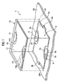
- the light emitting device 1 is provided with a mounting substrate 20 formed to have a recessed portion in its center, and with a light emitting element (an element) 10, such as a LED chip, mounted on the central recessed portion of the mounting substrate 20.
- a light emitting element an element 10
- a LED chip mounted on the central recessed portion of the mounting substrate 20.
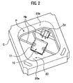
- the light emitting device 1 has a configuration comprising: a case C encompassing the recessed portion formed in the center of the mounting substrate 20; a wiring pattern Hp formed on the substrate's top face 20a where the light emitting element 10 is to be mounted in the center; the light emitting element 10 electrically connected, via an applied heat-melted connecting material kh such as solder paste, to the substrate electrodes (such as the first substrate electrode 2 and the second substrate electrodes 3) continuously connected to the wiring pattern Hp; and the light emitting element 10 covered with resin P, through which the device 1 gives off the light.
- the protective device Zd e.g. Zener diode
- the protective device Zd is also employed, whenever required, as part of the configuration comprising the device Zd mounted on the mounting substrate 20 in order to stabilize the performance of the light emitting element 10.
- the light emitting element 10 is mounted with the flip-chip method upon the first substrate electrode 2 and the second substrate electrodes 3 formed to be the mounted component on the top face 20a of the mounting substrate 20.
- the light emitting device 10 is provided, on one face thereof, with the light emitting section (the light producing section) 11, and, on the other face, with the first element electrode 12 and the second element electrodes 13.
- One example of the light emitting element 10 comprises a semiconductor light emitting element structure comprising at least: a light emitting layer; semiconductors in a laminated form (not shown in the figures), in which a first conduction type semiconductor, the light emitting layer, and a second conduction type semiconductor are formed in this order on the substrate; and electrodes formed to supply electric current to the laminated form of the semiconductors.
- the configuration of the light emitting device 10 is not limited to the above-mentioned configuration, and the device 10 may have another configuration, such as one having other semiconductor materials, or may be properly provided with protective layers or reflection layers (not shown in the figures).
- the light emitting device 10 may have a configuration in which a fluorescent material layer, made from fluorescent material or resin containing fluorescent material, covers the outer side of a semiconductor light emitting element structure (not shown in the figures) emitting a blue light.
- the white light emission is obtainable with the combination of a blue-light-emitting semiconductor light emitting element structure and a yellow-light-emitting cerium-activated YAG (yttrium/aluminium/garnet) type fluorescent material or a silicate fluorescent material such as (Sr, Ba) 2 SiO 4 :Eu.
- the color of the emitted light and the structure of the light emitting section 11 of the light emitting element 10 are not limited to this example as long as the section 11 is able to give off the light.
- the first element electrode 12 and the second element electrodes 13 are formed on the other face of the light emitting element 10 at positions inside the outer periphery of the element 10.
- the first element electrode 12 comprises one pair of opposing two sides defined by straight lines, and the other pair of opposing two sides provided with the recesses 12c, 12c, each of which is formed to be notched inward.
- the second element electrode 13 is formed in alignment with the recesses 12c of the first element electrode 12 at a position separated from the first element electrode 12.
- the second element electrodes 13 is formed into a D shape defined by a curved line in alignment with the curve of the recess 12c and by a straight line linking both ends of the curved line.
- the second element electrodes 13 is further disposed so that the straight line sections of the outer peripheries of the first and second element electrode 12, 13 may be precisely in line with each other.
- the material of the first element electrode 12 and the second element electrode 13 are not limited to this example, and any material generally used as an element electrode may be employed.
- the predetermined wiring pattern Hp (e.g. a substrate electrode) is formed together with the light emitting element 10 mounted on the substrate 20 via the heat-melted connecting material kh such as solder paste.
- the mounting substrate 20 has a configuration comprising metal-films laminated on a supporting substrate, which is made of laminated aluminium ceramic sheets.
- the mounting substrate 20 is provided, in the top face 20a formed into a concave shape in the predetermined positions on the substrate, with the first substrate electrode 2 and the second substrate electrode 3 formed into the shapes corresponding to the first element electrode 12 and the second electrode element 13 of the light emitting element 10, and with unillustrated external electrical connection terminals for an electrical connection with a driving circuit outside the device.
- the first substrate electrode 2 on the mounting substrate 20 is formed in the configuration comprising the electrode body 2a, which is the entire first substrate electrode 2 without the first extended sections 2b, 2b, so that the electrode body 2a is aligned to and identical with the first element electrode 12, which is a p-type electrode of the light emitting element 10.
- the straight line section of the outer periphery of the electrode 2 except the first extended section 2b, together with the curved line section are aligned to and identical with the outer periphery of the first element electrode.
- the first substrate electrode 2 is provided with the first extended sections 2b, 2b, each of which is formed on each of one pair of opposing two sides of the electrode 2a, and with the recesses 2c, 2c, each of which is formed on each of the other pair of opposing two sides of the electrode 2a.
- the objective of the first extended sections 2b, as well as the later mentioned first extended sections 3b of the second substrate electrode 3, is to prevent the generation of solder balls at the time of reflowing process.
- Each of the first extended sections 2b is formed in the center of each of one pair of opposing two sides of the electrode body 2a to extend farther outward than the outer periphery gs of the mounted light emitting element 10.
- the width L of the first extended sections 2b combined with the width of the later mentioned second extended sections 2d falls in the range between 10% or more and 50% or less of the length of the one side that is an assumed straight line of one side of the electrode body 2a of the first substrate electrode 2.
- the formation of the first extended sections 2b causes the heat-melted connecting material kh to run across the first extended sections 2b, allowing the surface tension of the heat-melted connecting material kh to prevent the generation of ball-looking substrates (solder balls).
- the extending length of the first extended section 2b is not limited to this example as long as the section 2b extends farther outward than the outer periphery gs of the light emitting element 10.
- the first extended section 2b may be formed to have a larger extending length in accordance with other components in the configuration.
- FIG. 3 shows the first extended section 2b having an edge section with a straight line, which is extended farther outward than the outer periphery gs of the element, and is formed into a strip-like rectangular shape, the shape of the edge section extended to gain a certain width of the section is not limited to this example.
- Each of the recesses 2c, 2c forms the area where the later mentioned second substrate electrode 3 is disposed, and is formed at the center of each of the other pair of sides of the electrode body 2a to be notched into a concave shape farther inward than the outer periphery of said electrode body 2a.
- the position, shape, size, and curvature of the recesses 2c, 2c are not limited to this example as long as the recesses are formed in accordance with the shape of the first element electrode 12 of the mounted light emitting element 10.
- the linear section (except the first extended section 2b) and the curved section of the recess 2c are formed aligned to and identical with, respectively, the linear section and the curved section of the recesses 12c in the outer periphery of the first element electrode 12 of the light emitting element 10.
- a more inwardly disposed curved portion of the recess 2c of the first substrate electrode 2 than the aligned recess 12c of the light emitting element 10 may allow the self-alignment around the section to leave the heat-melted connecting material kh having an inverted trapezoid cross section, which improves the connecting material kh's precision in the prevention of a short circuit between the electrodes.
- the second substrate electrodes 3 are formed, on the mounting substrate 20, in alignment with the recesses 2c, 2c of the first substrate electrode 2, and separated from the electrode 2 by a predetermined gap Sp.
- This second substrate electrode 3 is, in this example, formed into a D-shape, which is defined by the linear portion parallel to the linear portion (a single side) of the second element electrode 13 of the light emitting element 10 and by the curved portion corresponding to the curved portion of the first element electrode 12 as well as in alignment with the recess 2c of the first substrate electrode 2.
- the second substrate electrode 3 is also formed to have the first extended section 3b, which extends continuously from a connecting section 3a farther outward than the outer periphery of the light emitting element 10.
- This first extended section 3b is formed to place the portion, sandwiched between the linear section of the second substrate electrode 3 and the edge at the predetermined position of the extended section 3b, outside the periphery of the light emitting element 10, adding an extra portion to the essential area (of the second element electrode).
- the connecting section 3 a of the second substrate electrode 3 is a section which is aligned to the second element electrode 13.
- the first extended section 3b of the second substrate electrode 3 also refers to the section that is outer from the linear section of the electrode body 2a, and is continuously formed from the connecting section 3 a to occupy an area outside the outer periphery gs of the light emitting element 10. With respect to the extending length, the formed width, the shape, etc., the same conditions as the aforementioned first extended section 2b of the first substrate electrode 2 apply to the first extended section 3b. Note that the first extended section 3b of the second substrate electrode 3 is formed to have the width L (area) larger than that of the first extended section 2b of the first substrate electrode 2.
- the formation of the large width L is meant to prevent the generation of the solder balls coming from the surging portion of the heat-melted connecting material kh, which is more likely to surge around the electrode 3 due to the presence of the gap Sp between the first substrate electrode 2 and the second substrate electrode 3.
- the second substrate electrode 3, except the first extended section 3b, is aligned to the second element electrode 13, defining the positions of the electrodes with respect to each other.
- the first extended section 3b also refers to the entire strip section running along the linear section parallel to the outer periphery gs of the light emitting element 10.
- the outer periphery gs of the light emitting element 10 refers to the periphery defined by the outer sides of the laminating semiconductor structure in the plane, on which the first element electrode 12 and the second element electrode 13 are formed.
- the outer periphery of the first substrate electrode 2 and the second substrate electrode refer to the periphery forming the outer side of each of the electrodes.
- a device such as a protection device Zd, as well as the light emitting element 10, is mounted in a predetermined position.
- the mounting substrate 20 is formed as a part of the case C, whose side walls are defined by the concave shape formed to surround the center of the laminated sheets (for example, such process as ceramic packaging).
- the sheets underwent such processes as printing conductor patterns and, whenever it is necessary, perforation with piercing holes before the lamination.
- the light emitting element 10 is mounted together with other necessary members onto the top face 20a of the concave substrate of the light emitting device 1; then, the resin P, a sealing agent, is filled into the place where the light emitting element 10 is mounted.
- the choice of the embodiment of the case C of the light emitting device 1 is not limited to this example as long as the case can be usable for the case C of the light emitting device 1 like the one having an alumina ceramic or conductor patterns plated with a metal reflective to the light emitted from the light emitting element 10 (a metal such as Au or any silver-white colored metal, namely a reflective metal such as Ag or Al, is preferred).
- a metal such as Au or any silver-white colored metal, namely a reflective metal such as Ag or Al, is preferred.
- the sealing agent resin P seals the case C to confine the entire light emitting device 10 and the upper part of the recessed portion of the mounting substrate 20 (the top face 20a and a portion of the side faces forming the case C) as well as forming a lighting window above the recessed portion in the downstream of the light emitted from the light emitting device 1.
- the resin P prevents the open air from degrading the light emitting device 10.
- the disposition of the light emitting element 10 almost at the center of the resin P (or the external form thereof) in the point of a plan view can make the light from the light emitting element 10 emitted evenly towards the lighting window.
- the formation of the lighting window from the resin P into the surface of a hemisphere together with the disposition of the light emitting element 10 almost at the center of the hemisphere in the point of a plan view prevents the incidence angle of the incoming light at the hemisphere surface from exceeding the critical angle of incidence.
- the lighting window made from the resin P may have a desired shape, such as a hemisphere surface, a convex surface as a deformed sphere surface, a shell-type, or concave surface in order for the resin P to work as a lens to focus or diffuse the light.
- the resin comprises such materials as transparent resins and glass. Resins such as a hard silicone resin and epoxy resin are examples of viable resins P.
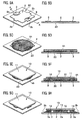
- FIG. 5 is assumed to illustrate the states of the recessed portion of the mounting substrate 20 formed into the shape of the case C.
- the electrode formation process comprises the formation of the first substrate electrode 2 and the second substrate electrode 3 on the mounting substrate 20.
- the first substrate electrode 2 and the second substrate electrode 3 are formed together with the other circuits on the mounting substrate 20 through a process such as exposure.
- the application process comprises the application of the heat-melted connecting material kh (e.g. solder paste) on the first substrate electrode 2 and the second substrate electrode 3 of the mounting substrate 20.
- the heat-melted connecting material kh e.g. solder paste
- the device mounting process comprises mounting the light emitting element 10 onto the heat-melted connecting material kh.
- part of the heat-melted connecting material kh is observed to jut out of the light emitting element 10.
- the reflowing process comprises heating of the heat-melted connecting material kh.
- the heat-melted connecting material kh is guided by the first extended sections 2b and 3b to smoothly run on the sections 2b and 3b.
- the surface tension of the connecting material kh prevents portion of the connecting material kh from being torn to drop into the outside of the extended sections. Therefore, as shown FIGS.
- the heat-melted connecting material kh is placed between the first element electrode 12 and the first substrate electrode 2 opposite to each other and between the second element electrode 13 and the second substrate electrode 3 opposite to each other as well as on the top face of the first extended sections 2b and 3b.
- the light emitting element 10 is mounted to be electronically and mechanically connected to the first substrate electrode 2 and the second substrate electrode 3 of the mounting substrate 20, solder balls are not generated.
- the light emitting element 10 is also shifted into a proper position due to the self-aligning motion caused by the surface tension of the heat-melted connecting material kh.
- a forced self-aligning motion may be attempted by deliberately displacing the light emitting element 10 from the proper mounting position by a predetermined rotational angle with respect to the first substrate electrode 2 and the second substrate electrode 3 to determine whether the light emitting element 10 actually undergoes the self alignment to be located into the proper position, which is driven by the applied heat in the reflowing process.
- the failure of the light emitting element 10 to undergo the self alignment may indicate that either the element 10 or the first substrate electrode 2 and the second electrode 3 have some defects.
- the configuration comprising the first substrate electrode 2 and the second substrate electrode 3 ensures the self alignment motion of the light emitting element 10 in the reflowing process, and the heat-melted connecting material kh is prevented from generating solder balls.
- the mounting of the light emitting element 10 and, optionally, other necessary devices (such as protective device Zd) on the mounting substrate 20 is followed by the filling with the resin P, the sealing agent, into the case C's recessed portion, where the light emitting element 10 is mounted, to produce the light emitting device 1.
- the production process of the light emitting device 1 is prevented from generating solder balls, and is less likely to be affected by the irregularity in mass assembly, and ensures the product's excellent quality.
- the lighting operations of the light emitting device 1 are as follows.
- the light emitting device 1 is connected to an unillustrated external driving circuit at the electric terminal for an external connection.
- the light emitting device 10 Via the metal film that is a wiring pattern wired on the top face 20a of the mounting substrate 20, the light emitting device 10, which is electrically connected to the first substrate electrode 2 and the second substrate electrode 3, is provided with electric power.
- the electric power supply prompts the light emitting element 10 to emit light cast outward from the light emitting element 10 via the resin P.
- FIG. 6 a preferred example of the configuration comprising the first substrate electrode 2 is the one illustrated in FIG. 6 .
- the same components as the aforementioned components of the light emitting device 1 are given the same reference numbers and the description of the identical components will be omitted.
- FIG. 6 differs from FIG. 3 in that the second extended sections 2d are further formed.
- the first substrate electrode 2 and the second substrate electrode 3 are separated from each other by the gap Sp. Therefore, in the reflowing process, the heat-melted connecting material kh is more likely to converge towards the second substrate electrode 3.
- the second extended section 2d is formed to be parts of the rim of the recess 2c, flanking the first extended section 3b on the two sides.
- the second extended sections 2d, 2d are formed to occupy the positions between the curved sections and the linear sections of the first substrate electrode 2 (the linear sections' ends closer to the second substrate electrode).
- the second extended section 2d is formed to have an equal extending length to the first extended section 3b of the second substrate electrode 3 to extend farther outward than the outer periphery gs of the light emitting element 10.
- the second extended section 2d is also formed to have a smaller width than the width L of the first extended section 3b.
- the second extended section 2d is formed to have the width which, when combined with the width of the first extended section 2b, does not exceed 50% of the length of one side of the first substrate electrode 2 assuming the end-to-end linearity of said side. Note that the reason why the combined width of the second extended section 2d and the first extended section 2b should not exceed said 50% is the same as previously presented for the first extended section 2b.
- the formation of the second extended section 2d prevents an excessive portion of the reflowing heat-melted connecting material kh from running toward the second substrate electrode 3; thus, the generation of defects such as voids in the heat-melted connecting material kh, sandwiched between the first element electrode 12 of the light emitting element 10 and the first substrate electrode 2, is also rendered preventable.
- the second extended section 2d is also formed likewise on the mounting substrate 20. It should be noted that the light emitting element 10 of this working example has an identical shape with the one illustrated in FIG. 2 .
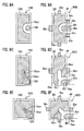
- the first substrate electrode 2A and the second substrate electrode 3A in the configuration illustrated in FIG. 7B may be also employable.
- the light emitting element 10A in the configuration illustrated in Fig. 7A is adopted according to the configuration comprising the first substrate electrode 2A and the second substrate electrode 3A.
- the previous description is valid to the relation of sizes between the first extended section 2b1 and the second extended section 2d1, and to their ratio to the length of the one side.
- FIG. 7A illustrates the light emitting element 10A provided with the light emitting section (not shown) on one face (on the front face), and with the first element electrode 12A and the second element electrode 13A on the other face.
- the entire surface inside the outer periphery forms an electrode provided with a plurality of the electrode recessed portions 12A1 formed with predetermined intervals.
- the first element electrode 12A is also provided with one pair of opposing linear sides A1 and A2 across the electrode and with the other pair of opposing sides A3 and A4 having the recesses 12c1 notched inward.
- the recess 12c1 comprises the semicircle concave section 12c11 and the concave grooves 12c12, 12c13, and 12c14. All the grooves extend continuously from the semicircle concave section 12c11 towards the side across the electrode or towards the adjacent sides.
- the concave groove 12c13 is formed to run parallel to the adjacent sides A1 and A2 with the depth of notch reaching around one third the way from the side A3 towards the side A4.
- the concave grooves 12c12 and 12c14 are formed to be symmetric with respect to the concave groove 12c13 at the center.
- the concave groove 12c12 is also formed to run towards the near center of the side A2 with the definite tilting angle to reach the almost same level of the notch depth as the concave groove 12c13 towards the side A4 across the electrode 12A.
- the concave groove 12c14 is also formed to run towards the near center of the side A1 with the definite tilting angle to reach the almost same level of the notch depth as the concave groove 12c13 towards the side A4 across the electrode 12A.
- Each of the second element electrodes 13A, 13A is formed to be disposed in the recess 12c1 of the first element electrode with the predetermined gap Sp.
- Each electrode 13A is formed into a shell-like shape defined by the linear section in line with the side A3 or A4 and by the curved section connecting the ends of the linear section in alignment with the recess 12c1.
- Each of the second element electrodes 13A, 13A is provided with the support electrode 13Aa, 13Ab, or 13Ac formed along the concave groove 12c12, 12c13, or 12c14.
- the recess 12c1 section which is the section comprising the semicircle concave section 12c11 and the concave grooves 12c12, 12c13, and 12c14 connected to the concave section 12c11 is covered by an insulating protective film (illustrated by vertical lines in a hatch pattern). Therefore, the surfaces of the second element electrodes 13A, 13A are separated from the surface of the first element electrode 12A by the insulating protective film, which allows the surface of the electrode 13A to be exposed without cover of the insulating protective film.
- the first substrate electrode 2A and the second substrate electrode 3A are connected to (mounted beneath) the first element electrode 12A and the second element electrode 13A via heat-melted connecting material kh (refer to FIG. 5 ).
- the first extended sections 2b1, 2b1 are formed respectively in one pair of the opposing sides B1, B2 across the electrode 2A, and the recesses 2c1, 2c1 are formed to be notched inward respectively in the other pair of the opposing sides B3, B4.
- the extended sections 2b1, 2b1 are in the identical shape as comprising the aforementioned first extended sections 2b, 2b, therefore, no further description of the sections 2b1 will be presented.
- Each of the recess 2c1, 2c1, is formed into a shape with a curved portion, which is aligned to and almost identical with the recess 12c1 of the first element electrode 12A, and comprises the semicircle concave section 2c11 and the concave grooves 2c12, 2c13, and 2c14 connected to the semicircle concave section 2c11 to extend towards the side across the electrode or towards the adjacent sides.
- the concave groove 2c13 is formed to run parallel to the adjacent sides B1 and B2 with the depth of notch reaching around one third the way from the side B3 towards the side B4.
- the concave grooves 2c12 and 2c14 are formed symmetric with respect to the concave groove 2c13 at the center.
- the concave groove 2c12 is also formed to run towards the near center of the side B2 with the definite tilting angle to reach the almost same level of the notch depth as the concave groove 2c13 towards the side B4 across the electrode 2A.
- the concave groove 2c14 is also formed to run towards the near center of the side B 1 with the necessary tilting angle to reach almost the same level of the notch depth as the concave groove 12c13 towards the side B4 across the electrode 2A.
- the second extended sections 2d1 are formed on both ends of the recess 2c1 to have an extending length shorter than the later mentioned first extended section 3b1 by d1 as illustrated and to have a width smaller than the later mentioned first extended section 3b1.
- the second substrate electrode 3A is formed into a shape of a rectangle with one side curved outward in alignment with the recess 2c1 of the first substrate electrode 2A.
- the curved side is aligned to and identical with the curved section of the second element electrode 13A.
- the second substrate electrode 3A is provided with the first extended section 3b1, formed to extend from the linear side, which is across the electrode 3A from the curved side, further outward than the outer periphery gs of the light emitting element 10A.
- the second substrate electrode 3A is provided with the connecting section 3a1 aligned to the second element electrode 13A and with the first extended section 3b1 continuously connected to the connecting section 3a1.
- the configuration prevents, while maintaining the self alignment, the convergence of the heat-melted connecting material kh towards the second substrate electrode, 3A rendering the generation of the solder balls of the heat-melted connecting material kh preventable.
- the shapes of the first element electrode 12a and the second element electrode 13A of the light emitting element 10A and the shape of the first substrate electrode 2A and the second substrate electrode 3A are formed so that the generation of solder balls of the heat-melted connecting material kh is very unlikely.
- the formation of the concave grooves 2c12, 2c13, 2c14 of the recesses of 2c1, 2c1 in the mounting substrate together with the formation of the concave grooves 12c12, 121c13, 12c14 of the recesses 12c1, 12c1 in the light emitting element 10A can enhance the self alignment performance.
- FIGS. 8A-8F may also prevent the generation of the solder balls while likewise maintaining self alignment as previously described.
- FIG. 8A illustrates the formation of the recess 12c2 notched inward in one of the longer sides of the rectangle of the first element electrode 12B of the light emitting element 10B, and the formation of the semicircular second element electrode 13B in alignment with the recess 12c2.
- the first substrate electrode 2B is in the configuration comprising the first extended sections 2b2, 2b2 formed in one pair of opposing sides across the electrode 2B, the first extended section 2b2 formed in one of the other pair of opposing sides, and second extended sections 2d2, 2d2 in the other side of said other pair together with the recess 2c2.
- the size and the width of the formed first extended section 2b2 are made larger in proportion with the length of each side.
- the second substrate electrode 3B is formed into a shape of a rectangle with one short side curving outward.
- the second substrate electrode 3B is provided with the first extended section 3b2 formed continuously connected to the connecting section 3a2 to extend further outward than the outer periphery gs of the light emitting element 10B.
- the objective of the present invention is also attainable even by the configuration comprising the second substrate electrode 3B disposed on only one side of the first substrate electrode 2B in alignment with the electrode configuration comprising the light emitting element 10B.
- FIG. 8C illustrates the light emitting element 10C provided with the first element electrode 12C comprising the recess 12c3 at one corner of the rectangle, and the second element electrode 13c disposed in alignment with the recess 12c3.
- the recess 12C3 comprises the concave groove 12c31 formed to run, in said first element electrode 12C, almost half the way towards a shorter side of the first element electrode 12C.
- FIG. 8D illustrates the first substrate electrode 2C provided with the recess 2c3 formed at one corner of the rectangle together with the first extended section 2b3 in each side.
- the concave groove 2b31 is formed to run, in said first substrate electrode 2C, almost half the way towards a shorter side of the first substrate electrode 2C.
- the longer sides and one of the shorter sides of the first substrate electrode 2C comprise the first extended sections 2b3 in the middle.
- the first extended section 2b3 is disposed to be continuously connected to the rim of the recess 2c3.
- the second substrate electrode 3C is formed into the shape of a rectangle with one round corner.
- the second substrate electrode 3C is provided with the first extended section 3b3 formed to be continuously connected to the connecting section 3a3 and to extend further outward than the outer periphery gs of the light emitting element 10C.
- the first extended section 2b3 formed in the second substrate electrode 3C is so formed as to be in line, in one of the four sides defining the rectangle of the light emitting element 10C, with the first extended section 3b3 of the second substrate electrode 3C.
- the first extended section 3b3 of the second substrate electrode 3C may extend further outward than the position marked by a solid line for the sake of connection to other wiring as indicated by the chain double-dashed lines.
- the first extended section 2b3 of the first substrate electrode 2 works also as the second extended section shown in FIG. 6 for the first extended section 3b3 of the second substrate electrode 3C. Because of the formation of one of the first substrate electrode 2C's first extended sections 2b3, in alignment with the second substrate electrode 3C and extending, from one of the rims of the recess 2c3, further outward than the outer periphery gs of the light emitting element 10C, the first extended section 2b3 can, due to the location it is formed, prevent the convergence of the heat-melted connecting material kh (refer to FIG. 5 ) towards the second substrate electrode 3C, which is also the objective of the second extended section 2d, while achieving the prime objective of the first extended section 2b3.
- the configuration illustrated in FIGS. 8E, 8F may be employed.
- the light emitting element 10D is provided with the recess 12c4 formed at one corner of the square, and with the first element electrode 12D with the second element electrode 13D disposed in alignment with the recess 12c4.
- the recess 12c4 comprises the concave groove 12c41 formed to run, in the first element electrode 12D, almost half the way (up to the center of the square) to the opposite corner across the first element electrode 12D.
- FIG. 8F illustrates the first substrate electrode 2D provided with the recess 2C4 formed at one corner of the square, and with the first extended section 2b4 in the middle of each side.
- the recess 2c4 is provided with the concave groove 2c41 formed to run, in the first substrate electrode 2D, almost half the way to the opposite corner across the first substrate electrode 2D.
- the first extended sections 2b4 of the first substrate electrode 2D are formed to have an identical width and extending length.
- the first substrate electrode 2D has a configuration comprising each of two first extended sections 2b4, 2b4 is formed on either rim of the recess 2c4.
- the second substrate electrode 3D is formed into a shape of a rectangle with one round corner.
- the second substrate electrode 3D is provided with the first extended section 3b4 formed to be continuously connected to the connecting section 3a4 and to extend further outward than the outer periphery gs of the light emitting element 10D.
- the first extended section 3b4 formed in the second substrate electrode 3D is formed so as to be in line, in one of the four sides of the rectangle (square) of the light emitting element 10D, with the first extended section 3b4 of the second substrate electrode 3D.
- the extended section 3b4 of the second substrate electrode 3D may extend further outward than the position marked by a solid line for the sake of connection to other wiring as indicated by the chain double-dashed lines.
- the first substrate electrode 2D's first extended section 2b4, 2b4 which flank the first extended section 3b4 of the second substrate electrode 3D on both sides, works also as the second extended section shown in FIG. 6 . Because of the formation of one of the first substrate electrode 2D's first extended sections 2b4, 2b4, in alignment with the second substrate electrode 3D and extending, from the rims of the recess 2c4, further outward than the outer periphery gs of the light emitting element 10D, the first extended section 2b4 can, due to the location it is formed, prevent the convergence of the reflowing heat-melted connecting material kh (refer to FIG. 5 ) towards the second substrate electrode 3C, which is also the objective of the second extended section 2d, while achieving the prime objective of the first extended section 2b4.
- the configuration may comprise the substrate electrode like 2C or 2D, in which the first extended section 2b3 or 2b4 is formed in alignment with one or two sides of the recess 2c3 or 2c4 flanking the second substrate electrode 3C or 3D.
- the configuration allows the first extended section 2b3 or 2b4 to achieve the objectives of the second extended section of the first substrate electrode as well as its prime objectives.
- FIGS. 9A and 9B also illustrate other possible examples of the already described first substrate electrode 2 and 2A, which have the third extended sections 102a, 102b on every corners.
- the same components as previously described are denoted by the same number, and their further description will be omitted.
- the first substrate electrode 2 is provided with the third extended sections 102a formed at the four corners, which extend further outward than the outer periphery gs of the light emitting element 10.
- the third extended section 102a is formed in such a way that the width of the first extended section 2b or the combined width of the first extended section 2b and the second extended section 2d may not exceed 50% of the length of the assumed straight line corresponding to one side of the first substrate electrode.
- the illustrated third extended section 102a in the figure having the shape of a rectangle connected to each corner may not exclude a third extended section having a round tip.
- the third extended section 102a may be formed at a corner of the already described first substrate electrode 2A.
- the third extended section 102a may be formed under the same conditions as already described.
- the provision of the first substrate electrodes 2 and 2A with the third extended section 102a causes the reflowing heat-melted connecting materials kh (refer to FIG. 4 , FIG. 5 ) to run on the third extended section 102a, therefore to be able to achieve an even height of the mounted light emitting device 10 even when an excessive amount of heat-melted connecting material kh is applied forming a thick layer.
- the excessive portion of the applied heat-melted connecting material kh is applied to cover the corners of the first substrate electrode 2, and 2A; therefore, only when an excessive amount is applied, the heat-melted connecting material may run on the third extended section 102a, and when a proper amount is applied, the third extended section 102a may remain unused.
- FIG. 10 also illustrates that the configuration comprising the first substrate electrode 52 and the second substrate 53 of the almost same size, and disposed adjacent to each other, can prevent the generation of the solder balls due to the formation of the first extended section 52b and 53b respectively on the first substrate electrode 52 and the first substrate electrode 53.
- the employed light emitting element 10E is also rectangle, and the first element electrode and the second element electrode (unillustrated) are formed in line inside the outer periphery gs.
- the self alignment via the heat-melted connecting material kh achieves the mounting of a light emitting element.
- the shape of one electrode body, electrode body 53a comprises linear sections while the shape of the other electrode body, electrode body 52a, comprises curved sections in order to avoid mistaking the anode for cathode due to the almost identical size of the first substrate electrode 52 and the second substrate electrode 53.
- the first extended sections 52b and 53b per one side of the rectangular light emitting element 10E are disposed to extend further outward than the outer periphery of the longer side of the light emitting element 10E. In this way, in the first substrate electrode 52 and the second substrate electrode 53, the increased ratio of the width of the first extended sections 52b and 53b combined to the longer side length is meant to prevent the generation of the solder balls.
- Two extended sections per one side of the light emitting element 10E are preferably disposed in positions symmetric with respect to the middle of said side.
- the formation of the first extended section or the second extended section (further of the third extended section) in the first substrate electrode and the second substrate electrode enables the prevention of the generation of the solder balls while maintaining the self alignment performance.
- the first extended section continuously connected to the connecting section comes out of the entire linear section of the width parallel to the outer periphery gs of the light emitting element 10
- the extended section may come out of only part of the linear section of the width comprising the outer periphery.
- the second substrate electrode comprises the first extended section formed to be continuously connected to the connecting section, and is shown as an enlarged part of the area aligned to and connected to the second element electrode.
- This configuration does not exclude the first extended section as a portion of the second substrate electrode, which has no enlarged area aligned to the second element electrode, and which is displaced so that the portion can extend farther outward than the periphery gs of the light emitting element 10.
- the configuration may comprise only the second extended section.
- the presence of the second extended section allows the surface tension of the heat-melted connecting material to reduce the generation of solder balls outside the mounting substrate.
- the light emitting device of the present invention is especially suited to applications for light sources for illumination, LED displays, lighting source for backlight for LCD, signals, lighting switches, various kinds of sensors and indicators, and auxiliary illuminants for motion pictures, as well as for other general consumer illuminants.
Landscapes
- Led Device Packages (AREA)
- Wire Bonding (AREA)
- Electric Connection Of Electric Components To Printed Circuits (AREA)
Applications Claiming Priority (2)
| Application Number | Priority Date | Filing Date | Title |
|---|---|---|---|
| JP2009166054A JP5585013B2 (ja) | 2009-07-14 | 2009-07-14 | 発光装置 |
| PCT/JP2010/059109 WO2011007621A1 (fr) | 2009-07-14 | 2010-05-28 | Dispositif electroluminescent |
Publications (3)
| Publication Number | Publication Date |
|---|---|
| EP2455966A1 true EP2455966A1 (fr) | 2012-05-23 |
| EP2455966A4 EP2455966A4 (fr) | 2014-11-26 |
| EP2455966B1 EP2455966B1 (fr) | 2017-11-08 |
Family
ID=43449230
Family Applications (1)
| Application Number | Title | Priority Date | Filing Date |
|---|---|---|---|
| EP10799683.7A Active EP2455966B1 (fr) | 2009-07-14 | 2010-05-28 | Dispositif électroluminescent |
Country Status (7)
| Country | Link |
|---|---|
| US (1) | US8614544B2 (fr) |
| EP (1) | EP2455966B1 (fr) |
| JP (1) | JP5585013B2 (fr) |
| KR (1) | KR101549720B1 (fr) |
| CN (1) | CN102473656B (fr) |
| TW (1) | TWI497778B (fr) |
| WO (1) | WO2011007621A1 (fr) |
Cited By (4)
| Publication number | Priority date | Publication date | Assignee | Title |
|---|---|---|---|---|
| EP2610926A1 (fr) * | 2011-12-26 | 2013-07-03 | Nichia Corporation | Procédé de fabrication d'un dispositif électroluminescent et dispositif électroluminescent |
| EP3196949A4 (fr) * | 2014-07-31 | 2018-01-24 | CCS Inc. | Substrat de montage de led et led |
| EP3595022A1 (fr) * | 2018-07-13 | 2020-01-15 | Stanley Electric Co., Ltd. | Élément optique semi-conducteur |
| US10843284B2 (en) | 2014-12-18 | 2020-11-24 | Zkw Group Gmbh | Method for void reduction in solder joints |
Families Citing this family (23)
| Publication number | Priority date | Publication date | Assignee | Title |
|---|---|---|---|---|
| US9722157B2 (en) * | 2010-04-09 | 2017-08-01 | Rohm Co., Ltd. | LED module |
| JP5753734B2 (ja) * | 2011-05-19 | 2015-07-22 | 日本特殊陶業株式会社 | 配線基板、多数個取り配線基板、およびその製造方法 |
| JP5706254B2 (ja) | 2011-07-05 | 2015-04-22 | 株式会社東芝 | 半導体装置 |
| JP5275528B1 (ja) * | 2011-11-22 | 2013-08-28 | パナソニック株式会社 | 半導体発光装置 |
| DE102012215705B4 (de) * | 2012-09-05 | 2021-09-23 | OSRAM Opto Semiconductors Gesellschaft mit beschränkter Haftung | Gehäuse für ein optisches bauelement, baugruppe, verfahren zum herstellen eines gehäuses und verfahren zum herstellen einer baugruppe |
| JP6107136B2 (ja) | 2012-12-29 | 2017-04-05 | 日亜化学工業株式会社 | 発光装置用パッケージ及びそれを備える発光装置、並びにその発光装置を備える照明装置 |
| KR102037866B1 (ko) * | 2013-02-05 | 2019-10-29 | 삼성전자주식회사 | 전자장치 |
| ITBO20130063A1 (it) * | 2013-02-14 | 2014-08-15 | Spal Automotive Srl | Macchina elettrica. |
| US9548261B2 (en) * | 2013-03-05 | 2017-01-17 | Nichia Corporation | Lead frame and semiconductor device |
| JP6286857B2 (ja) * | 2013-04-10 | 2018-03-07 | 三菱電機株式会社 | 照明ランプおよび照明装置 |
| JP6484396B2 (ja) * | 2013-06-28 | 2019-03-13 | 日亜化学工業株式会社 | 発光装置用パッケージ及びそれを用いた発光装置 |
| JP2015207754A (ja) * | 2013-12-13 | 2015-11-19 | 日亜化学工業株式会社 | 発光装置 |
| TW201543720A (zh) * | 2014-05-06 | 2015-11-16 | 新世紀光電股份有限公司 | 封裝結構及其製備方法 |
| JP6578735B2 (ja) * | 2014-05-21 | 2019-09-25 | 日亜化学工業株式会社 | 半導体装置の実装構造、バックライト装置及び実装基板 |
| KR20170059068A (ko) * | 2015-11-19 | 2017-05-30 | 삼성전자주식회사 | 광원 모듈, 디스플레이 패널 및 이를 구비한 디스플레이 장치 |
| JP6572757B2 (ja) | 2015-11-30 | 2019-09-11 | 日亜化学工業株式会社 | 発光装置 |
| JP6128267B2 (ja) * | 2016-06-10 | 2017-05-17 | 日亜化学工業株式会社 | 半導体素子実装部材及び半導体装置 |
| KR102654925B1 (ko) | 2016-06-21 | 2024-04-05 | 삼성디스플레이 주식회사 | 디스플레이 장치 및 이의 제조 방법 |
| JP2018032748A (ja) | 2016-08-24 | 2018-03-01 | パナソニックIpマネジメント株式会社 | 発光装置、照明装置及び発光装置の製造方法 |
| US10667396B2 (en) | 2017-08-25 | 2020-05-26 | Tactotek Oy | Multilayer structure for hosting electronics and related method of manufacture |
| JP6652117B2 (ja) | 2017-11-29 | 2020-02-19 | 日亜化学工業株式会社 | 樹脂パッケージおよび発光装置 |
| JP7111957B2 (ja) | 2018-06-14 | 2022-08-03 | 日亜化学工業株式会社 | 半導体装置及びその製造方法 |
| JP7502659B2 (ja) * | 2021-12-23 | 2024-06-19 | 日亜化学工業株式会社 | 発光装置および基板 |
Family Cites Families (18)
| Publication number | Priority date | Publication date | Assignee | Title |
|---|---|---|---|---|
| JPH06120648A (ja) | 1992-10-08 | 1994-04-28 | Murata Mfg Co Ltd | チップ状電子部品の半田付け方法 |
| JP3326292B2 (ja) * | 1994-05-24 | 2002-09-17 | 株式会社東芝 | 通信機器及びその通信方法 |
| JP3252605B2 (ja) * | 1994-07-04 | 2002-02-04 | 株式会社村田製作所 | 電子部品及びその製造方法 |
| EP0907308B1 (fr) * | 1996-05-29 | 2011-01-26 | Rohm Co., Ltd. | Procedes de montage de bornes sur une plaquette de circuit et plaquette de circuit munies de bornes |
| JP3860364B2 (ja) * | 1999-08-11 | 2006-12-20 | 富士通メディアデバイス株式会社 | 弾性表面波装置 |
| TW472367B (en) * | 2000-12-12 | 2002-01-11 | Siliconware Precision Industries Co Ltd | Passive device pad design for avoiding solder pearls |
| CN1464953A (zh) | 2001-08-09 | 2003-12-31 | 松下电器产业株式会社 | Led照明装置和卡型led照明光源 |
| JP2007059930A (ja) | 2001-08-09 | 2007-03-08 | Matsushita Electric Ind Co Ltd | Led照明装置およびカード型led照明光源 |
| US7242033B2 (en) * | 2002-03-08 | 2007-07-10 | Rohm Co., Ltd. | Semiconductor device using LED chip |
| JP3924481B2 (ja) * | 2002-03-08 | 2007-06-06 | ローム株式会社 | 半導体チップを使用した半導体装置 |
| JP3877642B2 (ja) * | 2002-05-21 | 2007-02-07 | ローム株式会社 | 半導体チップを使用した半導体装置 |
| CN1759492B (zh) * | 2003-03-10 | 2010-04-28 | 丰田合成株式会社 | 固体元件装置的制造方法 |
| JP4029843B2 (ja) * | 2004-01-19 | 2008-01-09 | 豊田合成株式会社 | 発光装置 |
| JP4637160B2 (ja) * | 2003-03-10 | 2011-02-23 | 豊田合成株式会社 | 固体素子デバイスの製造方法 |
| JP2007059781A (ja) | 2005-08-26 | 2007-03-08 | Toyoda Gosei Co Ltd | サブマウント付発光素子および発光装置 |
| EP1966833A1 (fr) * | 2005-12-19 | 2008-09-10 | Showa Denko K.K. | Dispositif electroluminescent a semi-conducteur de type puce retournee, procede de fabrication de ce dispositif, carte de circuit imprime pour ce dispositif, structure de montage de ce dispositif et lampe a diode electroluminescente |
| JP2007258605A (ja) * | 2006-03-24 | 2007-10-04 | Toshiba Corp | 部品内蔵プリント配線板、部品内蔵プリント配線板の製造方法および電子機器 |
| JP4962217B2 (ja) * | 2007-08-28 | 2012-06-27 | 富士通株式会社 | プリント配線基板及び電子装置製造方法 |
-
2009
- 2009-07-14 JP JP2009166054A patent/JP5585013B2/ja active Active
-
2010
- 2010-05-28 US US13/383,815 patent/US8614544B2/en active Active
- 2010-05-28 WO PCT/JP2010/059109 patent/WO2011007621A1/fr not_active Ceased
- 2010-05-28 CN CN201080031891.7A patent/CN102473656B/zh active Active
- 2010-05-28 KR KR1020117028955A patent/KR101549720B1/ko active Active
- 2010-05-28 EP EP10799683.7A patent/EP2455966B1/fr active Active
- 2010-07-02 TW TW099121925A patent/TWI497778B/zh active
Cited By (6)
| Publication number | Priority date | Publication date | Assignee | Title |
|---|---|---|---|---|
| EP2610926A1 (fr) * | 2011-12-26 | 2013-07-03 | Nichia Corporation | Procédé de fabrication d'un dispositif électroluminescent et dispositif électroluminescent |
| EP3196949A4 (fr) * | 2014-07-31 | 2018-01-24 | CCS Inc. | Substrat de montage de led et led |
| US10843284B2 (en) | 2014-12-18 | 2020-11-24 | Zkw Group Gmbh | Method for void reduction in solder joints |
| EP3595022A1 (fr) * | 2018-07-13 | 2020-01-15 | Stanley Electric Co., Ltd. | Élément optique semi-conducteur |
| CN110718616A (zh) * | 2018-07-13 | 2020-01-21 | 斯坦雷电气株式会社 | 光半导体元件 |
| US10937937B2 (en) | 2018-07-13 | 2021-03-02 | Stanley Electric Co., Ltd. | Optical semiconductor element |
Also Published As
| Publication number | Publication date |
|---|---|
| TWI497778B (zh) | 2015-08-21 |
| JP2011023484A (ja) | 2011-02-03 |
| KR101549720B1 (ko) | 2015-09-02 |
| TW201130172A (en) | 2011-09-01 |
| EP2455966A4 (fr) | 2014-11-26 |
| CN102473656A (zh) | 2012-05-23 |
| JP5585013B2 (ja) | 2014-09-10 |
| US20120112622A1 (en) | 2012-05-10 |
| CN102473656B (zh) | 2015-09-02 |
| KR20120048535A (ko) | 2012-05-15 |
| WO2011007621A1 (fr) | 2011-01-20 |
| US8614544B2 (en) | 2013-12-24 |
| EP2455966B1 (fr) | 2017-11-08 |
Similar Documents
| Publication | Publication Date | Title |
|---|---|---|
| EP2455966B1 (fr) | Dispositif électroluminescent | |
| US7923739B2 (en) | Solid state lighting device | |
| JP5554680B2 (ja) | 発光素子搭載用基板、発光装置およびこれらの製造方法 | |
| US20090090928A1 (en) | Light emitting module and method for manufacturing the same | |
| US7866853B2 (en) | Light-emitting element mounting substrate and manufacturing method thereof, light-emitting element module and manufacturing method thereof, display device, lighting device, and traffic light | |
| CN103460415A (zh) | 发光器件封装、系统和方法 | |
| JP2008147605A (ja) | 発光装置及びその製造方法並びに実装基板 | |
| JP2009524930A (ja) | 発光ダイオードパッケージ及びその製造方法 | |
| JP2004253404A (ja) | 発光素子収納用パッケージおよび発光装置 | |
| US10903399B2 (en) | Method for manufacturing a light emitting device comprising at least two first light emitting diodes and a second light emitting diodes interposed therebetween | |
| US20260101619A1 (en) | Led package structure | |
| JP5697091B2 (ja) | 半導体発光装置 | |
| JP4945416B2 (ja) | 発光モジュール及びその製造方法 | |
| EP2023407A1 (fr) | Substrat de montage de dispositif luminescent et procede pour le produire, module de dispositif luminescent et procede pour le fabriquer, affichage, dispositif d'eclairage, et systeme de signalisation pour la circulation | |
| JP2009094322A (ja) | 発光装置 | |
| US20100065874A1 (en) | Light emitting device | |
| JP2013045842A (ja) | 発光装置 | |
| US10283489B2 (en) | Light emitting device | |
| KR20140042187A (ko) | 발광 장치 | |
| KR20100028033A (ko) | 발광장치 및 발광장치용 패키지 집합체 | |
| KR101815963B1 (ko) | 칩 패키지 및 칩 패키지 제조방법 | |
| JP4628877B2 (ja) | 発光素子実装用ホーロー基板、発光素子モジュール、照明装置、表示装置及び交通信号機 | |
| JP2007116107A (ja) | 発光装置 | |
| KR101931318B1 (ko) | 칩 패키지 | |
| JP2025146264A (ja) | 発光装置 |
Legal Events
| Date | Code | Title | Description |
|---|---|---|---|
| PUAI | Public reference made under article 153(3) epc to a published international application that has entered the european phase |
Free format text: ORIGINAL CODE: 0009012 |
|
| 17P | Request for examination filed |
Effective date: 20120208 |
|
| AK | Designated contracting states |
Kind code of ref document: A1 Designated state(s): AL AT BE BG CH CY CZ DE DK EE ES FI FR GB GR HR HU IE IS IT LI LT LU LV MC MK MT NL NO PL PT RO SE SI SK SM TR |
|
| DAX | Request for extension of the european patent (deleted) | ||
| A4 | Supplementary search report drawn up and despatched |
Effective date: 20141024 |
|
| RIC1 | Information provided on ipc code assigned before grant |
Ipc: H01L 23/00 20060101ALI20141020BHEP Ipc: H01L 33/62 20100101ALN20141020BHEP Ipc: H01L 33/38 20100101AFI20141020BHEP |
|
| 17Q | First examination report despatched |
Effective date: 20160112 |
|
| REG | Reference to a national code |
Ref country code: DE Ref legal event code: R079 Ref document number: 602010046585 Country of ref document: DE Free format text: PREVIOUS MAIN CLASS: H01L0021600000 Ipc: H01L0033380000 |
|
| RIC1 | Information provided on ipc code assigned before grant |
Ipc: H01L 33/38 20100101AFI20170320BHEP Ipc: H01L 23/00 20060101ALI20170320BHEP Ipc: H01L 33/62 20100101ALN20170320BHEP |
|
| GRAP | Despatch of communication of intention to grant a patent |
Free format text: ORIGINAL CODE: EPIDOSNIGR1 |
|
| INTG | Intention to grant announced |
Effective date: 20170606 |
|
| GRAS | Grant fee paid |
Free format text: ORIGINAL CODE: EPIDOSNIGR3 |
|
| GRAA | (expected) grant |
Free format text: ORIGINAL CODE: 0009210 |
|
| AK | Designated contracting states |
Kind code of ref document: B1 Designated state(s): AL AT BE BG CH CY CZ DE DK EE ES FI FR GB GR HR HU IE IS IT LI LT LU LV MC MK MT NL NO PL PT RO SE SI SK SM TR |
|
| REG | Reference to a national code |
Ref country code: GB Ref legal event code: FG4D |
|
| REG | Reference to a national code |
Ref country code: CH Ref legal event code: EP Ref country code: AT Ref legal event code: REF Ref document number: 944932 Country of ref document: AT Kind code of ref document: T Effective date: 20171115 |
|
| REG | Reference to a national code |
Ref country code: IE Ref legal event code: FG4D |
|
| REG | Reference to a national code |
Ref country code: DE Ref legal event code: R096 Ref document number: 602010046585 Country of ref document: DE |
|
| REG | Reference to a national code |
Ref country code: NL Ref legal event code: MP Effective date: 20171108 |
|
| REG | Reference to a national code |
Ref country code: LT Ref legal event code: MG4D |
|
| REG | Reference to a national code |
Ref country code: FR Ref legal event code: PLFP Year of fee payment: 9 |
|
| REG | Reference to a national code |
Ref country code: AT Ref legal event code: MK05 Ref document number: 944932 Country of ref document: AT Kind code of ref document: T Effective date: 20171108 |
|
| PG25 | Lapsed in a contracting state [announced via postgrant information from national office to epo] |
Ref country code: NO Free format text: LAPSE BECAUSE OF FAILURE TO SUBMIT A TRANSLATION OF THE DESCRIPTION OR TO PAY THE FEE WITHIN THE PRESCRIBED TIME-LIMIT Effective date: 20180208 Ref country code: FI Free format text: LAPSE BECAUSE OF FAILURE TO SUBMIT A TRANSLATION OF THE DESCRIPTION OR TO PAY THE FEE WITHIN THE PRESCRIBED TIME-LIMIT Effective date: 20171108 Ref country code: NL Free format text: LAPSE BECAUSE OF FAILURE TO SUBMIT A TRANSLATION OF THE DESCRIPTION OR TO PAY THE FEE WITHIN THE PRESCRIBED TIME-LIMIT Effective date: 20171108 Ref country code: ES Free format text: LAPSE BECAUSE OF FAILURE TO SUBMIT A TRANSLATION OF THE DESCRIPTION OR TO PAY THE FEE WITHIN THE PRESCRIBED TIME-LIMIT Effective date: 20171108 Ref country code: SE Free format text: LAPSE BECAUSE OF FAILURE TO SUBMIT A TRANSLATION OF THE DESCRIPTION OR TO PAY THE FEE WITHIN THE PRESCRIBED TIME-LIMIT Effective date: 20171108 Ref country code: LT Free format text: LAPSE BECAUSE OF FAILURE TO SUBMIT A TRANSLATION OF THE DESCRIPTION OR TO PAY THE FEE WITHIN THE PRESCRIBED TIME-LIMIT Effective date: 20171108 |
|
| PG25 | Lapsed in a contracting state [announced via postgrant information from national office to epo] |
Ref country code: BG Free format text: LAPSE BECAUSE OF FAILURE TO SUBMIT A TRANSLATION OF THE DESCRIPTION OR TO PAY THE FEE WITHIN THE PRESCRIBED TIME-LIMIT Effective date: 20180208 Ref country code: IS Free format text: LAPSE BECAUSE OF FAILURE TO SUBMIT A TRANSLATION OF THE DESCRIPTION OR TO PAY THE FEE WITHIN THE PRESCRIBED TIME-LIMIT Effective date: 20180308 Ref country code: HR Free format text: LAPSE BECAUSE OF FAILURE TO SUBMIT A TRANSLATION OF THE DESCRIPTION OR TO PAY THE FEE WITHIN THE PRESCRIBED TIME-LIMIT Effective date: 20171108 Ref country code: GR Free format text: LAPSE BECAUSE OF FAILURE TO SUBMIT A TRANSLATION OF THE DESCRIPTION OR TO PAY THE FEE WITHIN THE PRESCRIBED TIME-LIMIT Effective date: 20180209 Ref country code: AT Free format text: LAPSE BECAUSE OF FAILURE TO SUBMIT A TRANSLATION OF THE DESCRIPTION OR TO PAY THE FEE WITHIN THE PRESCRIBED TIME-LIMIT Effective date: 20171108 Ref country code: LV Free format text: LAPSE BECAUSE OF FAILURE TO SUBMIT A TRANSLATION OF THE DESCRIPTION OR TO PAY THE FEE WITHIN THE PRESCRIBED TIME-LIMIT Effective date: 20171108 |
|
| PG25 | Lapsed in a contracting state [announced via postgrant information from national office to epo] |
Ref country code: CZ Free format text: LAPSE BECAUSE OF FAILURE TO SUBMIT A TRANSLATION OF THE DESCRIPTION OR TO PAY THE FEE WITHIN THE PRESCRIBED TIME-LIMIT Effective date: 20171108 Ref country code: SK Free format text: LAPSE BECAUSE OF FAILURE TO SUBMIT A TRANSLATION OF THE DESCRIPTION OR TO PAY THE FEE WITHIN THE PRESCRIBED TIME-LIMIT Effective date: 20171108 Ref country code: CY Free format text: LAPSE BECAUSE OF FAILURE TO SUBMIT A TRANSLATION OF THE DESCRIPTION OR TO PAY THE FEE WITHIN THE PRESCRIBED TIME-LIMIT Effective date: 20171108 Ref country code: EE Free format text: LAPSE BECAUSE OF FAILURE TO SUBMIT A TRANSLATION OF THE DESCRIPTION OR TO PAY THE FEE WITHIN THE PRESCRIBED TIME-LIMIT Effective date: 20171108 Ref country code: DK Free format text: LAPSE BECAUSE OF FAILURE TO SUBMIT A TRANSLATION OF THE DESCRIPTION OR TO PAY THE FEE WITHIN THE PRESCRIBED TIME-LIMIT Effective date: 20171108 |
|
| REG | Reference to a national code |
Ref country code: DE Ref legal event code: R097 Ref document number: 602010046585 Country of ref document: DE |
|
| PG25 | Lapsed in a contracting state [announced via postgrant information from national office to epo] |
Ref country code: RO Free format text: LAPSE BECAUSE OF FAILURE TO SUBMIT A TRANSLATION OF THE DESCRIPTION OR TO PAY THE FEE WITHIN THE PRESCRIBED TIME-LIMIT Effective date: 20171108 Ref country code: PL Free format text: LAPSE BECAUSE OF FAILURE TO SUBMIT A TRANSLATION OF THE DESCRIPTION OR TO PAY THE FEE WITHIN THE PRESCRIBED TIME-LIMIT Effective date: 20171108 Ref country code: SM Free format text: LAPSE BECAUSE OF FAILURE TO SUBMIT A TRANSLATION OF THE DESCRIPTION OR TO PAY THE FEE WITHIN THE PRESCRIBED TIME-LIMIT Effective date: 20171108 Ref country code: IT Free format text: LAPSE BECAUSE OF FAILURE TO SUBMIT A TRANSLATION OF THE DESCRIPTION OR TO PAY THE FEE WITHIN THE PRESCRIBED TIME-LIMIT Effective date: 20171108 |
|
| PLBE | No opposition filed within time limit |
Free format text: ORIGINAL CODE: 0009261 |
|
| STAA | Information on the status of an ep patent application or granted ep patent |
Free format text: STATUS: NO OPPOSITION FILED WITHIN TIME LIMIT |
|
| 26N | No opposition filed |
Effective date: 20180809 |
|
| PG25 | Lapsed in a contracting state [announced via postgrant information from national office to epo] |
Ref country code: SI Free format text: LAPSE BECAUSE OF FAILURE TO SUBMIT A TRANSLATION OF THE DESCRIPTION OR TO PAY THE FEE WITHIN THE PRESCRIBED TIME-LIMIT Effective date: 20171108 |
|
| REG | Reference to a national code |
Ref country code: CH Ref legal event code: PL |
|
| REG | Reference to a national code |
Ref country code: BE Ref legal event code: MM Effective date: 20180531 |
|
| PG25 | Lapsed in a contracting state [announced via postgrant information from national office to epo] |
Ref country code: MC Free format text: LAPSE BECAUSE OF FAILURE TO SUBMIT A TRANSLATION OF THE DESCRIPTION OR TO PAY THE FEE WITHIN THE PRESCRIBED TIME-LIMIT Effective date: 20171108 |
|
| REG | Reference to a national code |
Ref country code: IE Ref legal event code: MM4A |
|
| PG25 | Lapsed in a contracting state [announced via postgrant information from national office to epo] |
Ref country code: LI Free format text: LAPSE BECAUSE OF NON-PAYMENT OF DUE FEES Effective date: 20180531 Ref country code: CH Free format text: LAPSE BECAUSE OF NON-PAYMENT OF DUE FEES Effective date: 20180531 |
|
| PG25 | Lapsed in a contracting state [announced via postgrant information from national office to epo] |
Ref country code: LU Free format text: LAPSE BECAUSE OF NON-PAYMENT OF DUE FEES Effective date: 20180528 |
|
| PG25 | Lapsed in a contracting state [announced via postgrant information from national office to epo] |
Ref country code: IE Free format text: LAPSE BECAUSE OF NON-PAYMENT OF DUE FEES Effective date: 20180528 |
|
| PG25 | Lapsed in a contracting state [announced via postgrant information from national office to epo] |
Ref country code: BE Free format text: LAPSE BECAUSE OF NON-PAYMENT OF DUE FEES Effective date: 20180531 |
|
| PG25 | Lapsed in a contracting state [announced via postgrant information from national office to epo] |
Ref country code: MT Free format text: LAPSE BECAUSE OF NON-PAYMENT OF DUE FEES Effective date: 20180528 |
|
| PG25 | Lapsed in a contracting state [announced via postgrant information from national office to epo] |
Ref country code: TR Free format text: LAPSE BECAUSE OF FAILURE TO SUBMIT A TRANSLATION OF THE DESCRIPTION OR TO PAY THE FEE WITHIN THE PRESCRIBED TIME-LIMIT Effective date: 20171108 |
|
| PG25 | Lapsed in a contracting state [announced via postgrant information from national office to epo] |
Ref country code: HU Free format text: LAPSE BECAUSE OF FAILURE TO SUBMIT A TRANSLATION OF THE DESCRIPTION OR TO PAY THE FEE WITHIN THE PRESCRIBED TIME-LIMIT; INVALID AB INITIO Effective date: 20100528 Ref country code: PT Free format text: LAPSE BECAUSE OF FAILURE TO SUBMIT A TRANSLATION OF THE DESCRIPTION OR TO PAY THE FEE WITHIN THE PRESCRIBED TIME-LIMIT Effective date: 20171108 |
|
| PG25 | Lapsed in a contracting state [announced via postgrant information from national office to epo] |
Ref country code: MK Free format text: LAPSE BECAUSE OF NON-PAYMENT OF DUE FEES Effective date: 20171108 |
|
| PG25 | Lapsed in a contracting state [announced via postgrant information from national office to epo] |
Ref country code: AL Free format text: LAPSE BECAUSE OF FAILURE TO SUBMIT A TRANSLATION OF THE DESCRIPTION OR TO PAY THE FEE WITHIN THE PRESCRIBED TIME-LIMIT Effective date: 20171108 |
|
| REG | Reference to a national code |
Ref country code: FR Ref legal event code: PLFP Year of fee payment: 14 |
|
| P01 | Opt-out of the competence of the unified patent court (upc) registered |
Effective date: 20230522 |
|
| REG | Reference to a national code |
Ref country code: DE Ref legal event code: R079 Ref document number: 602010046585 Country of ref document: DE Free format text: PREVIOUS MAIN CLASS: H01L0033380000 Ipc: H10H0020831000 |
|
| PGFP | Annual fee paid to national office [announced via postgrant information from national office to epo] |
Ref country code: DE Payment date: 20250402 Year of fee payment: 16 |
|
| PGFP | Annual fee paid to national office [announced via postgrant information from national office to epo] |
Ref country code: FR Payment date: 20250401 Year of fee payment: 16 |
|
| PGFP | Annual fee paid to national office [announced via postgrant information from national office to epo] |
Ref country code: GB Payment date: 20260323 Year of fee payment: 17 |