EP2469221A1 - Procédé et système pour configurer un dispositif pour corriger l'effet d'un milieu sur un signal lumineux, procédé, dispositif et système pour corriger cet effet. - Google Patents
Procédé et système pour configurer un dispositif pour corriger l'effet d'un milieu sur un signal lumineux, procédé, dispositif et système pour corriger cet effet. Download PDFInfo
- Publication number
- EP2469221A1 EP2469221A1 EP10196310A EP10196310A EP2469221A1 EP 2469221 A1 EP2469221 A1 EP 2469221A1 EP 10196310 A EP10196310 A EP 10196310A EP 10196310 A EP10196310 A EP 10196310A EP 2469221 A1 EP2469221 A1 EP 2469221A1
- Authority
- EP
- European Patent Office
- Prior art keywords
- signal
- optical element
- medium
- correcting
- interference
- Prior art date
- Legal status (The legal status is an assumption and is not a legal conclusion. Google has not performed a legal analysis and makes no representation as to the accuracy of the status listed.)
- Ceased
Links
- 238000000034 method Methods 0.000 title claims abstract description 63
- 230000000694 effects Effects 0.000 title claims abstract description 25
- 230000003287 optical effect Effects 0.000 claims abstract description 118
- 230000000644 propagated effect Effects 0.000 claims abstract description 26
- 230000001902 propagating effect Effects 0.000 claims abstract description 22
- 238000005457 optimization Methods 0.000 description 14
- 238000010586 diagram Methods 0.000 description 4
- 230000004048 modification Effects 0.000 description 4
- 238000012986 modification Methods 0.000 description 4
- 238000005259 measurement Methods 0.000 description 3
- 230000001360 synchronised effect Effects 0.000 description 3
- 230000005540 biological transmission Effects 0.000 description 2
- 230000007423 decrease Effects 0.000 description 2
- 239000011159 matrix material Substances 0.000 description 2
- 239000013307 optical fiber Substances 0.000 description 2
- 230000010355 oscillation Effects 0.000 description 2
- 230000003068 static effect Effects 0.000 description 2
- 238000010420 art technique Methods 0.000 description 1
- 230000009466 transformation Effects 0.000 description 1
Images


Classifications
-
- G—PHYSICS
- G02—OPTICS
- G02F—OPTICAL DEVICES OR ARRANGEMENTS FOR THE CONTROL OF LIGHT BY MODIFICATION OF THE OPTICAL PROPERTIES OF THE MEDIA OF THE ELEMENTS INVOLVED THEREIN; NON-LINEAR OPTICS; FREQUENCY-CHANGING OF LIGHT; OPTICAL LOGIC ELEMENTS; OPTICAL ANALOGUE/DIGITAL CONVERTERS
- G02F1/00—Devices or arrangements for the control of the intensity, colour, phase, polarisation or direction of light arriving from an independent light source, e.g. switching, gating or modulating; Non-linear optics
- G02F1/01—Devices or arrangements for the control of the intensity, colour, phase, polarisation or direction of light arriving from an independent light source, e.g. switching, gating or modulating; Non-linear optics for the control of the intensity, phase, polarisation or colour
- G02F1/0121—Operation of devices; Circuit arrangements, not otherwise provided for in this subclass
-
- G—PHYSICS
- G02—OPTICS
- G02B—OPTICAL ELEMENTS, SYSTEMS OR APPARATUS
- G02B26/00—Optical devices or arrangements for the control of light using movable or deformable optical elements
- G02B26/06—Optical devices or arrangements for the control of light using movable or deformable optical elements for controlling the phase of light
Definitions
- the present invention relates to a method and a system for configuring a device for correcting the effect of a medium on a light signal having propagated through said medium.
- the invention also relates to a method, a device and a system for correcting said effect.
- the signal at the output of the medium is a disordered or blurred version of the light signal input to the medium.
- the modification applied by the medium must be corrected in order to recover the information conveyed by the light signal.
- a device comprising several reflexion elements separated by a static propagation medium may be used to realise any spatial transformation on a light signal ( Programmable Unitary Spatial Modes Manipulation , Jean-Pierre Morizur, Lachlan Nicholls, Pu Jian, Seiji Armstrong, Nicolas Treps, Boris Hage, Magnus Hsu, Warwick Bowen, Jiri Janousek, Hans-A. Bachor ) .
- Another object of the present invention is to provide a method and a system making it possible to efficiently correct the effect of a medium on a light signal having propagated through said medium.
- Another object is furthermore to provide an industrially applicable method and a system making it possible to correct the effect of a medium on a light signal having propagated through said medium.
- Another object is furthermore to provide a method and a system making it possible to correct the effect of a medium on a light signal having propagated through said medium in a faster and inexpensive fashion.
- Yet another object of the invention is to provide a method and a system making possible a complete correction of the effect of a medium on a light signal having propagated through said medium.
- Such objects are accomplished through a method for configuring a device to correct the effect of a medium on a light signal having propagated through said medium, said device comprising at least one optical element whose spatial phase profile _is individually adjustable, said method comprising several iterations of the following steps:
- medium it is meant a medium or a combination of media, each medium being a natural or artificial medium.
- a single optical element comprising independent sections whose phase profiles are individually adjustable, may be used to perform several successive reflexions or phase changes, in order to avoid the use of several such optical elements.
- the method according to the invention makes it possible to configure a device to efficiently and completely correct the effect of a medium on a light signal having propagated through said medium.
- the present invention provides a method that is simple to implement.
- the configuration of the correcting device is entirely based on the disordered signal propagated through the correcting device and doesn't comprise any computation of the transmission matrix of the medium.
- the errors that may be caused by such a computation operation are avoided and the method according to the invention is industrially applicable, less expensive and less time consuming than the prior art techniques.
- the reference signal may be propagated through the device in the same or opposite direction to that of the disordered signal.
- the step of measuring an interference parameter may comprise a step of measuring for each optical element:
- a pixel is defined as the smallest area of an optical element for which it is possible to modify the phase profile.
- the interference parameter may comprise a parameter relative to the phase difference between the disordered signal and the reference signal.
- the interference parameter may comprise a parameter relative to the phase of the interference signal at each pixel or zone of the optical element.
- the interference parameter may comprise, for an optical element, a parameter relative to the intensity of the interference signal, more particularly the light intensity, for each pixel or zone of the optical element, or the total light intensity, of the interference signal obtained by interference of the reference signal and the disordered signal.
- the total light intensity of the interference signal for an optical element corresponds to the sum of the intensities measured for all the zones or pixels of the optical element.
- the light intensity of the interference between the disordered signal and the reference signal may be used to measure the powers and the phase difference between these two signals.
- the method according to the invention may comprise a step to oscillate in time the overall phase of the reference signal and/or first signal.
- Such a modulation makes the intensity of the interference between the disordered signal and the reference signal oscillate in time. For each zone of the optical element where the intensity of the interference is measured the local phase difference relative to the other zones between the reference signal and the disordered signal can be computed.
- phase of the interference signal at each pixel or zone of the optical element with respect to a reference pixel or a predetermined phase reference is used to decide the necessary modification to the phase profile of this pixel or zone.
- the step of modifying the spatial phase profile of an optical element may comprise modifying the phase delay applied by at least one zone and/or at least one pixel of said optical element to a light signal.
- a feature of the method according to the invention is that the reference signal, the first signal or both the reference signal and the first signal may be modulated spatially before propagating through the medium and the correcting device.
- the method according to the invention may comprise a step to modulate the intensity profile of the reference signal and/or first signal.
- the method according to the invention may also comprise a step to produce the reference signal and the first signal from two or more spatially separated incoherent light sources. Indeed this incoherence is equivalent to a spatial modulation of the overall source.
- Such a spatial modulation makes it possible to configure the device, more particularly the spatial phase profile of each optical element, so that any effect of any complex medium on any light signal is corrected. Indeed, if the reference and first signals were not spatially modulated, then the spatial profile of the reference and first signals would remain static. The correcting device would then be configured according to only one spatial profile and would be able to correct the disordered signal only for one spatial profile.
- the method according to the invention may also comprise a step for measuring a visibility parameter.
- an overall phase modulation applied to the reference signal or the disordered signal makes it possible to measure an interference visibility parameter between the reference signal and the disordered signal.
- an interference visibility parameter may be measured at a given position, for instance before, after or in the correcting device as the interference visibility parameter measured between two light signals remains identical whatever the measurement position.
- the reference signal is phase modulated before propagating through the correcting device.
- An interference parameter is measured for each pixel of each optical element.
- the measured interference parameter is the intensity of the interference signal.
- the intensity of the interference signal measured at each pixel of an optical element oscillates in time.
- phase difference between these oscillations and the reference oscillation measured at a pixel with high intensity is calculated.
- phase difference By modifying the phase delay applied by each pixel of an optical element, the phase difference are reduced to 0 and all the oscillating interference signals measured for the optical element are synchronised. This synchronisation increases the visibility of the interference between the reference signal and the disordered signal.
- the optimization step may be conducted individually for each optical element and one after each other whatever the order.
- the method according to the invention may also comprise a step of generating the first signal and the reference signal from a unique light signal.
- the light signal may be divided into two light signals, one being the first signal and the other the reference signal.
- the invention also relates to a device for correcting the effect of a medium on a light signal having propagated through said medium, comprising at least one optical element whose spatial phase profile is individually adjustable and configured according to the configuration method according to the invention.
- the two optical elements are separated by a combination of lenses and free space propagation.
- At least one optical element is a spatial light modulator or a deformable mirror.
- the invention also relates to a method for correcting the effect of a medium on a light signal having propagated through said medium, said method implementing a device comprising at least one optical element whose phase profile is individually adjustable, said method comprising:
- the correcting method according to the present invention may also comprise at least one adjusting step for adjusting the configuration of the device if changes occur in the medium during the correcting phase.
- a control light signal is sent regularly through the system to readjust the device, using the configuration method.
- This control light signal can be different from the light signal used in the configuration phase.
- the control light signal is sent through the output of the device, and is reflected at the input of the complex medium.
- the control light goes through the correcting device, the medium, the medium again and finally the correcting device again.
- the device corrects the effect of the medium. Additional small changes occurring in the medium can be corrected using the calibration method with the control light.
- the invention also relates to a system for configuring a device for correcting the effect of a medium on a light signal having propagated through said medium, said device comprising at least one optical element whose spatial phase profile is individually adjustable, said system comprising:
- the means for propagating the reference signal may be adapted to propagate the reference signal through the device in the opposite direction to that of the disordered signal
- the system according to the invention may also comprise modulation means to introduce an overall phase modulation on the reference signal or the disordered signal before propagating said signal through the correcting device.
- the system according to the invention may also comprise an element to modulate the spatial profile of the reference signal, the first signal or both these signals before they are sent in the medium or the correcting device.
- the measuring means may comprise one CCD camera or one CCD camera for each optical element.
- Such a CCD camera may be configured for measuring an interference parameter for each pixel of the optical element.
- the system according to the invention may also comprise reflexion means to transmit to the CCD camera a part of the interference signal obtained by interference of the disordered signal and the reference signal.
- the means for modifying the phase profile of an optical element may comprise at least one actuator for each optical element, more particularly an actuator for each zone or pixel of each optical element. Such actuators may be integrated to the optical elements.
- the invention also relates to a system for correcting the effect of a medium on a light signal having propagated through said medium, said system comprising:
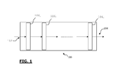
- FIGURE 1 schematically represents an example of a correcting device.
- the correcting device 100 comprises at least one input 102 and at least one output 104.
- the correcting device 100 comprises several optical elements 106 1 -106 n .
- Each optical element 106 has an adjustable spatial phase profile.
- each optical element 106 may be a spatial phase modulator (SLM) or a deformable mirror (DM).
- SLM spatial phase modulator
- DM deformable mirror
- Each optical element 106 is separated from another optical element 106 by free space propagation and a lens (not represented), which perform an optical transform.
- a disordered signal is input to the correcting device 100 and propagates across the optical elements 106 one after another. After the last optical element 106 n , the disordered signal is corrected and the correcting device provides the corrected version of the disordered signal.
- the several optical elements 106 1 -106 n may be replaced by independent section of a single optical element, i.e. a spatial phase modulator or a deformable mirror.
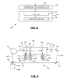
- FIGURE 2 is a block diagram of an embodiment of the configuration method according to the invention.
- the configuration method 200 comprises a first step 202 of generation of a light signal.
- the spatial profile of the light signal is modulated using an accousto-optic modulator, a simple chopper or another mean to change the spatial profile of the light.
- the spatial modulation may be random.
- the light signal is divided into two identical light signals called the first signal and the reference signal.
- the first signal is propagated through a medium, and thus a disordered signal is obtained at the output of the medium.
- the reference signal is phase modulated.
- the disordered signal and the reference signal are propagated through the correcting device, i.e. the optical elements, in opposite directions.
- the propagation of the disordered signal and the modulated reference signal through each optical element generates an interference signal at each optical element, and more particularly at each pixel of each optical element.
- step 212 an optimization of the interference between the disordered signal and the modulated reference signal is performed.
- the optimization step 212 comprises a step 214 measuring an interference parameter, i.e. the light intensity of the interference signal, for each pixel of an optical element of the correcting device. For each pixel, the measured intensity of the interference signal oscillates due to the phase modulation of the reference signal. Thus, for a given optical element there are as many oscillating signals as pixel.
- an interference parameter i.e. the light intensity of the interference signal
- the optimization step 212 also comprises a step 216 for modifying the spatial phase profile of the considered optical element in order to synchronise all the measured oscillating signals.
- the synchronisation for an optical element may be performed as follows.
- a reference pixel is chosen among all the pixels of the optical element.
- a reference phase may be chosen and the phase delay for each pixel may be determined by comparing the phase of the interference signal of each pixel to the reference phase.
- Steps 214 and 216 are realised for each optical element of the correcting device whatever the order. This condition is verified at step 218 that makes sure that steps 214 and 216 are realised for all optical elements of the correcting device.
- a second interference parameter i.e. the interference visibility
- the interference visibility value is tested.
- other measurements can be used as termination parameters such as the contrast of the output image of the system, a local contrast of the output image, the fidelity to a desired intensity profile, the fidelity to a desired phase profile, the fidelity to a desired intensity and phase profile, the symmetry of the output image, the asymmetry of the output image, the phase differences measured at different points in the device, the intensity profiles measured at different points in the device.
- the optimization step 212 is repeated until a satisfactory value of the interference visibility is obtained.
- FIGURE 3 is a block diagram of an embodiment of the correction method according to the invention.
- the correction method 300 represented en figure 3 comprises a configuration phase 302, configuring a correction device as the device 100 represented on figure 1 and realised according to the configuration method 200 represented en figure 2 .
- the correction method 300 also comprises a correcting phase 304, after the configuration phase 302.
- the correcting phase comprises a step 306 for correcting a disordered signal with the configuration device.
- the correcting phase also comprises a step 308 for adjusting the configuration of the device if changes occur on the medium during the correcting step. Then the correcting step 306 is stopped. The adjusting step 308 is realised. When the adjusting step 308 is finished the correcting step 308 is continued.
- FIGURE 4 schematically represents a correcting system 400 according to the invention.
- the correcting system 400 represented on figure 4 comprises a source 402 providing a spatially modulated light signal 404.
- the light signal 404 is divided into two equal and identical light signals by a semi-reflective mirror 406.
- a first light signal 408 and a reference light signal 410 are obtained.
- the first light signal 408 is propagated through the medium 412 and a disordered light signal 414 is obtained at the output of the medium 412.
- the reference signal 410 is entered into a phase modulator 516 thanks to two reflective mirrors 418 and 420.
- the disordered signal 414 is propagated through the correcting device 100 from the input 102 to the output 104 and crosses all the optical elements 106 from the first optical element 106 1 to the last optical element 106 n .
- the modulated reference signal 410 is propagated through the correcting device 100 from the output 104 to the input 102 and crosses all the optical elements 106 from the last optical element 106 n to the first optical element 106 1 .
- the propagation of the disordered signal 414 and the modulated reference signal 410 causes an interference signal in the correcting device, for instance at each optical element 106.
- the system 400 comprises an optimization module 418 1 -418 n for each optical element.
- Each optimization module 418 i comprises a CCD camera 420 i measuring the amplitude of the interference signal for each pixel of the optical element 106 i and at least one actuator 422 i adapted to modify the phase profile of each pixel of the optical element 106 i .
- the actuator 422 i realizes a stochastic modification of the phase delay applied by each pixel of the optical element 106 i .
- the optimization is realised for every optical element 106 one after another. For example, the optimization is realised for the first optical element 106 1 , then the second optical element 106 2 and so on. When one optimization step is realised for each element, then a first optimization cycle is completed. A second optimization cycle is then realised and so on.
- the optimization is stopped when a desired value of the interference visibility is reached, for example 0.95.
- the order in which the optimization is realised on the optical elements 106 is not important.
- FIGURE 5 is a schematic representation of the means for measuring the amplitude of the interference signal for each pixel of an optical element.
- the CCD camera 422 i is adapted and configured to measure the intensity of the interference signal for each pixel 502 of the pixels 502 1 -502 p of the optical element 106 i .
- the intensity of the interference signal is measured in the same way for each pixel 502 j of the optical element 106 i .
- the disordered signal 414 is reflected on a semi-reflective mirror 504 i associated to the optical element 106 i .
- a part 414 1 of the disordered signal having crossed the pixel 502 j of the optical element 106 i is projected to the CCC camera 422 i .
- a second part 414 2 continues to propagate to the optical element 106 i+1 .
- the modulated reference signal 410 coming from the optical element 106 i+1 and going to cross the pixel 502 j of the optical element 106 i is reflected on the semi reflective mirror 504 i .
- a part 410 1 of the modulated reference signal 410 is then reflected to a mirror 506 i which in turn reflects this part 410 1 of the modulated reference signal 410 to the CCD camera 422 i .
- a second part 410 2 continues to propagate to the optical element 106 i , more particularly to the pixel 502 j of the optical element 106 i .
- the intensity of the interference signal is measured by the CCD camera 522 for each pixel 502 of each optical element 106.
- FIGURE 6 schematically represents the intensity of the interference signal measured for each pixel of an optical element, for example at the step 214 of the configuration method represented on figure 2 .
- the oscillating curves 604 1 , 604 j and 604 p on the graph 602 of figure 6 schematically represent the intensity of the interference signal measured for the pixels 1, j and p of an optical element 106 before calibration.
- the oscillating intensity curves 604 are not synchronised and the total intensity, i.e. the sum of the intensity measured for each pixel, does not oscillate. It means that the value of the interference visibility parameter is 0.
- the oscillating curves 604 1 , 604 j and 604 p on the graph 606 of figure 6 schematically represent the intensity of the interference signal measured for the pixels 1, j and p of an optical element 106 after calibration.
- the oscillating amplitude curves 604 are well synchronised and the total intensity, i.e. the sum of the intensity measured for each pixel is maximal.
- the device is well configured and is able to correct the disordered signal and recover the initial signal.
- the invention is particularly adapted to correct the effect of an optical fibre on a light signal.
Landscapes
- Physics & Mathematics (AREA)
- General Physics & Mathematics (AREA)
- Optics & Photonics (AREA)
- Nonlinear Science (AREA)
- Optical Modulation, Optical Deflection, Nonlinear Optics, Optical Demodulation, Optical Logic Elements (AREA)
- Mechanical Light Control Or Optical Switches (AREA)
- Optical Communication System (AREA)
Priority Applications (10)
| Application Number | Priority Date | Filing Date | Title |
|---|---|---|---|
| EP10196310A EP2469221A1 (fr) | 2010-12-21 | 2010-12-21 | Procédé et système pour configurer un dispositif pour corriger l'effet d'un milieu sur un signal lumineux, procédé, dispositif et système pour corriger cet effet. |
| PCT/EP2011/073535 WO2012085046A1 (fr) | 2010-12-21 | 2011-12-21 | Procédé et système pour configurer un dispositif pour corriger l'effet d'un milieu sur un signal lumineux, procédé, dispositif et système pour corriger ledit effet |
| CA2821106A CA2821106C (fr) | 2010-12-21 | 2011-12-21 | Procede et systeme pour configurer un dispositif pour corriger l'effet d'un milieu sur un signal lumineux, procede, dispositif et systeme pour corriger ledit effet |
| BR112013015061A BR112013015061A2 (pt) | 2010-12-21 | 2011-12-21 | método e sistema para configurar um dispositivo para corrigir o efeito de um meio em um sinal luminoso, método, aparelho e sistema para corrigir o referido efeito |
| US13/993,805 US9250454B2 (en) | 2010-12-21 | 2011-12-21 | Method and system for configuring a device for correcting the effect of a medium on a light signal, method, device and system for correcting said effect |
| EP11813327.1A EP2656003B1 (fr) | 2010-12-21 | 2011-12-21 | Procédé et système pour configurer un dispositif pour corriger l'effet d'un milieu sur un signal lumineux, procédé, dispositif et système pour corriger ledit effet |
| CN201180061009.8A CN103299154B (zh) | 2010-12-21 | 2011-12-21 | 对用于校正介质对光信号的作用的设备进行配置的方法和系统、用于校正该作用的方法、设备和系统 |
| AU2011347385A AU2011347385C1 (en) | 2010-12-21 | 2011-12-21 | Method and system for configuring a device for correcting the effect of a medium on a light signal, method, device and system for correcting said effect |
| US15/854,566 USRE48338E1 (en) | 2010-12-21 | 2011-12-21 | Method and system for configuring a device for correcting the effect of a medium on a light signal, method, device and system for correcting said effect |
| JP2013554802A JP5990544B2 (ja) | 2010-12-21 | 2011-12-21 | 光信号に対する媒質の作用を補正するデバイスの構成方法及び構成システム、前記作用の補正方法、補正デバイス及び補正システム |
Applications Claiming Priority (1)
| Application Number | Priority Date | Filing Date | Title |
|---|---|---|---|
| EP10196310A EP2469221A1 (fr) | 2010-12-21 | 2010-12-21 | Procédé et système pour configurer un dispositif pour corriger l'effet d'un milieu sur un signal lumineux, procédé, dispositif et système pour corriger cet effet. |
Publications (1)
| Publication Number | Publication Date |
|---|---|
| EP2469221A1 true EP2469221A1 (fr) | 2012-06-27 |
Family
ID=44065284
Family Applications (2)
| Application Number | Title | Priority Date | Filing Date |
|---|---|---|---|
| EP10196310A Ceased EP2469221A1 (fr) | 2010-12-21 | 2010-12-21 | Procédé et système pour configurer un dispositif pour corriger l'effet d'un milieu sur un signal lumineux, procédé, dispositif et système pour corriger cet effet. |
| EP11813327.1A Active EP2656003B1 (fr) | 2010-12-21 | 2011-12-21 | Procédé et système pour configurer un dispositif pour corriger l'effet d'un milieu sur un signal lumineux, procédé, dispositif et système pour corriger ledit effet |
Family Applications After (1)
| Application Number | Title | Priority Date | Filing Date |
|---|---|---|---|
| EP11813327.1A Active EP2656003B1 (fr) | 2010-12-21 | 2011-12-21 | Procédé et système pour configurer un dispositif pour corriger l'effet d'un milieu sur un signal lumineux, procédé, dispositif et système pour corriger ledit effet |
Country Status (8)
| Country | Link |
|---|---|
| US (2) | USRE48338E1 (fr) |
| EP (2) | EP2469221A1 (fr) |
| JP (1) | JP5990544B2 (fr) |
| CN (1) | CN103299154B (fr) |
| AU (1) | AU2011347385C1 (fr) |
| BR (1) | BR112013015061A2 (fr) |
| CA (1) | CA2821106C (fr) |
| WO (1) | WO2012085046A1 (fr) |
Cited By (4)
| Publication number | Priority date | Publication date | Assignee | Title |
|---|---|---|---|---|
| FR3061964A1 (fr) * | 2017-01-19 | 2018-07-20 | Cailabs | Transformation de la variation d'un parametre d'un faisceau en la variation d'un autre de ses parametres |
| CN109716198A (zh) * | 2016-06-17 | 2019-05-03 | 索邦大学 | 以可控的光强度照射物体的装置及相关方法 |
| WO2020021196A1 (fr) * | 2018-07-25 | 2020-01-30 | Cailabs | Dispositif de traitement d'un rayonnement lumineux comprenant un dispositif de conversion de lumiere multiplan |
| FR3084480A1 (fr) * | 2018-07-25 | 2020-01-31 | Cailabs | Dispositif de traitement d’un rayonnement lumineux comprenant un dispositif de conversion de lumière multiplan |
Families Citing this family (24)
| Publication number | Priority date | Publication date | Assignee | Title |
|---|---|---|---|---|
| FR3016973B1 (fr) | 2014-01-30 | 2017-08-11 | Cailabs | Dispositif de traitement d'un rayonnement lumineux/optique, procede et systeme de conception d'un tel dispositif |
| FR3025957B1 (fr) | 2014-09-11 | 2016-12-23 | Cailabs | Dispositif et procede de compensation de dispersion chromatique |
| US10073221B2 (en) * | 2015-09-30 | 2018-09-11 | Nokia Of America Corporation | Beamforming for an optical switch |
| FR3049134B1 (fr) | 2016-03-15 | 2018-07-13 | Cailabs | Dispositf de communications par fibre optique multimode avec interversion de modes de propagation |
| FR3049135B1 (fr) | 2016-03-15 | 2020-02-14 | Cailabs | Dispositf de communications par fibre optique multimode avec composant de compensation de dispersion modale |
| FR3076358B1 (fr) | 2017-12-28 | 2019-12-20 | Cailabs | Dispositif optique disposant de moyens pour son assemblage precis, procede d'assemblage ou de test de ce dispositif |
| FR3076357B1 (fr) | 2017-12-29 | 2021-10-22 | Cailabs | Cavite multi passage d’un dispositif optique de manipulation spatiale d’un rayonnement lumineux. |
| FR3078412B1 (fr) | 2018-02-26 | 2022-01-14 | Cailabs | Procede de conception d’un dispositif de conversion multiplan, lame de phase obtenus par l’intermediaire de ce procede, et dispositif de conversion multiplan |
| FR3092404B1 (fr) | 2019-02-04 | 2021-10-22 | Cailabs | Dispositif optique de combinaison d'une pluralite de faisceaux, et systeme employant un tel dispositif |
| FR3097334A1 (fr) | 2019-06-17 | 2020-12-18 | Cailabs | Procédé de fixation d’une fibre optique monomode et d’une fibre optique multimode, equipement de couplage optique et fibre optique pouvant être obtenue grace à un tel procédé |
| FR3097659B1 (fr) | 2019-06-21 | 2024-04-19 | Cailabs | Source lumineuse comportant au moins une puce à semi-conducteur portant au moins une diode |
| FR3104271B1 (fr) | 2019-12-04 | 2021-12-17 | Alpao | Systeme d’optique adaptative a temps de reponse ameliore, utilisation et procede afferents |
| FR3106668B1 (fr) | 2020-01-29 | 2022-01-21 | Cailabs | Dispositif de traitement d’un faisceau lumineux par l'intermediaire d’un convertisseur multi plan pour le conformer à une forme prédéterminée |
| FR3120450B1 (fr) | 2021-03-04 | 2023-11-24 | Cailabs | Système de compensation de la distorsion d’un front d’onde d’un rayonnement lumineux incident |
| WO2022246695A1 (fr) * | 2021-05-26 | 2022-12-01 | The University Of Hong Kong | Amélioration de la communication à espace libre classique et quantique par optique adaptative et par séparation des faisceaux de référence et de signal |
| FR3128798B1 (fr) | 2021-10-28 | 2025-01-17 | Cailabs | Dispositif de traitement d’au moins deux Faisceaux lumineux monomodes |
| FR3129002A1 (fr) | 2021-11-05 | 2023-05-12 | Safran Electrical & Power | Dispositif de connexion par réattribution de canal de transmission à un réseau fibré passif de communication multiplexé embarqué pour aéronef |
| FR3129221A1 (fr) | 2021-11-15 | 2023-05-19 | Safran Electrical & Power | Multiplexeur optique hybride, démultiplexeur optique hybride associé et réseau de communication optique embarqué associé |
| FR3137189B1 (fr) | 2022-06-27 | 2025-03-14 | Cailabs | Cavite multi passage d’un dispositif optique de manipulation spatiale d’un rayonnement lumineux |
| FR3142310B1 (fr) | 2022-11-21 | 2025-10-24 | Cailabs | Système de telecommunication optique en espace libre |
| FR3147876A1 (fr) | 2023-04-14 | 2024-10-18 | Cailabs | Système photonique comprenant une puce photonique et un dispositif de conversion multiplan |
| FR3148885A1 (fr) | 2023-05-19 | 2024-11-22 | Cailabs | Dispositif de traitement optique d’un rayonnement lumineux incident s’etant propage en espace libre |
| FR3148886A1 (fr) | 2023-05-19 | 2024-11-22 | Cailabs | Systeme de telecommunication optique en espace libre |
| FR3154512A1 (fr) | 2023-10-24 | 2025-04-25 | Cailabs | Dispositif optique de combinaison cohérente et Système employant un tel dispositif pour éclairer une cible en champ lointain |
Citations (2)
| Publication number | Priority date | Publication date | Assignee | Title |
|---|---|---|---|---|
| US5090795A (en) * | 1987-10-22 | 1992-02-25 | Hughes Aircraft Company | Integrated adaptive optics apparatus |
| EP0562424A1 (fr) * | 1992-03-25 | 1993-09-29 | Texas Instruments Incorporated | Systéme integré d'étalonnage optique |
Family Cites Families (23)
| Publication number | Priority date | Publication date | Assignee | Title |
|---|---|---|---|---|
| JPS5582621U (fr) | 1978-11-30 | 1980-06-07 | ||
| JPS56114936A (en) | 1980-02-18 | 1981-09-09 | Canon Inc | Focusing plate |
| JPH06250108A (ja) | 1993-02-22 | 1994-09-09 | Hitachi Ltd | 補償光学装置とこれを用いた天体望遠鏡,光データリンク,レーザ加工機 |
| JPH08189806A (ja) | 1995-01-11 | 1996-07-23 | Fuji Xerox Co Ltd | 干渉計測方法および干渉計 |
| US5717516A (en) * | 1996-03-01 | 1998-02-10 | Hughes Electronics | Hybrid laser power combining and beam cleanup system using nonlinear and adaptive optical wavefront compensation |
| US6200309B1 (en) * | 1997-02-13 | 2001-03-13 | Mcdonnell Douglas Corporation | Photodynamic therapy system and method using a phased array raman laser amplifier |
| US6275250B1 (en) * | 1998-05-26 | 2001-08-14 | Sdl, Inc. | Fiber gain medium marking system pumped or seeded by a modulated laser diode source and method of energy control |
| IL130904A (en) * | 1998-08-11 | 2004-07-25 | Trw Inc | Fiber laser system with high average power with phase front control |
| JP4350186B2 (ja) | 1999-01-06 | 2009-10-21 | オリンパス株式会社 | 合焦装置 |
| JP3455775B2 (ja) | 2000-07-27 | 2003-10-14 | 独立行政法人産業技術総合研究所 | 光駆動型波面補正映像方法及び装置 |
| US6519385B1 (en) * | 2000-09-27 | 2003-02-11 | The Boeing Company | Method and apparatus for controllably positioning an optical fiber to introduce a phase shift |
| US6430328B1 (en) | 2000-10-13 | 2002-08-06 | William H. Culver | Optical switch |
| DE60123468T2 (de) * | 2000-12-22 | 2007-08-02 | Danmarks Tekniske Universitet | Verfahren und vorrichtung zur erzeugung einer phasenmodulierten wellenfront elektromagnetischer strahlung |
| US6597836B2 (en) * | 2001-06-20 | 2003-07-22 | The Boeing Company | Optical phased array control system |
| CN100397147C (zh) | 2001-10-25 | 2008-06-25 | 滨松光子学株式会社 | 相位调制装置和相位调制方法 |
| JP2004045326A (ja) | 2002-07-15 | 2004-02-12 | Konica Minolta Holdings Inc | 干渉計装置 |
| US7027161B2 (en) | 2002-12-26 | 2006-04-11 | Hrl Laboratories, Llc | Adaptive optical system with self-referencing contrast control |
| US7194155B1 (en) | 2004-08-10 | 2007-03-20 | The Board Of Trustees Of The Leland Stanford Junior University | Adaptive control for mitigating interference in a multimode transmission medium |
| US7154658B2 (en) | 2005-04-08 | 2006-12-26 | The Boeing Company | Wavefront correction system |
| JP4819403B2 (ja) | 2005-06-06 | 2011-11-24 | 株式会社トプコン | 距離測定装置 |
| WO2009100113A1 (fr) * | 2008-02-07 | 2009-08-13 | Imra America, Inc. | Réseaux de fibres parallèles à haute puissance |
| JP2009216454A (ja) | 2008-03-07 | 2009-09-24 | Canon Inc | 波面収差測定装置、波面収差測定方法、露光装置およびデバイス製造方法 |
| CN101271575B (zh) | 2008-04-09 | 2010-06-02 | 东华大学 | 用于工业近景摄影中测量图像的正投影化校正方法 |
-
2010
- 2010-12-21 EP EP10196310A patent/EP2469221A1/fr not_active Ceased
-
2011
- 2011-12-21 EP EP11813327.1A patent/EP2656003B1/fr active Active
- 2011-12-21 US US15/854,566 patent/USRE48338E1/en active Active
- 2011-12-21 AU AU2011347385A patent/AU2011347385C1/en active Active
- 2011-12-21 CN CN201180061009.8A patent/CN103299154B/zh active Active
- 2011-12-21 WO PCT/EP2011/073535 patent/WO2012085046A1/fr not_active Ceased
- 2011-12-21 CA CA2821106A patent/CA2821106C/fr active Active
- 2011-12-21 JP JP2013554802A patent/JP5990544B2/ja active Active
- 2011-12-21 BR BR112013015061A patent/BR112013015061A2/pt not_active Application Discontinuation
- 2011-12-21 US US13/993,805 patent/US9250454B2/en not_active Ceased
Patent Citations (2)
| Publication number | Priority date | Publication date | Assignee | Title |
|---|---|---|---|---|
| US5090795A (en) * | 1987-10-22 | 1992-02-25 | Hughes Aircraft Company | Integrated adaptive optics apparatus |
| EP0562424A1 (fr) * | 1992-03-25 | 1993-09-29 | Texas Instruments Incorporated | Systéme integré d'étalonnage optique |
Non-Patent Citations (3)
| Title |
|---|
| JEAN-FRANÇOIS MORIZUR ET AL: "Programmable unitary spatial mode manipulation", JOURNAL OF THE OPTICAL SOCIETY OF AMERICA A, vol. 27, no. 11, 1 November 2010 (2010-11-01), pages 2524 - 2531, XP055000594, ISSN: 1084-7529, DOI: 10.1364/JOSAA.27.002524 * |
| S. M. POPOFF ET AL: "Measuring the Transmission Matrix in Optics: An Approach to the Study and Control of Light Propagation in Disordered Media", PHYSICAL REVIEW LETTERS, vol. 104, no. 10, 8 March 2010 (2010-03-08), XP055000592, ISSN: 0031-9007, DOI: 10.1103/PhysRevLett.104.100601 * |
| VELLEKOOP I M: "Exploiting disorder for perfect focusing", NATURE PHOTONICS, vol. 4, 1 May 2010 (2010-05-01), NATURE PUBLISHING GROUP, GB, pages 320 - 322, XP009149181, ISSN: 1749-4885, [retrieved on 20100214], DOI: 10.1038/NPHOTON.2010.3 * |
Cited By (10)
| Publication number | Priority date | Publication date | Assignee | Title |
|---|---|---|---|---|
| CN109716198A (zh) * | 2016-06-17 | 2019-05-03 | 索邦大学 | 以可控的光强度照射物体的装置及相关方法 |
| CN109716198B (zh) * | 2016-06-17 | 2022-10-04 | 索邦大学 | 以可控的光强度照射物体的装置及相关方法 |
| FR3061964A1 (fr) * | 2017-01-19 | 2018-07-20 | Cailabs | Transformation de la variation d'un parametre d'un faisceau en la variation d'un autre de ses parametres |
| WO2018134534A1 (fr) | 2017-01-19 | 2018-07-26 | Cailabs | Separateur optique a ratio variable pour controler la proportion d'energie d'un faisceau lumineux |
| WO2018134533A1 (fr) | 2017-01-19 | 2018-07-26 | Cailabs | Dispositif pour changer la forme d'un faisceau lumineux |
| WO2018134532A1 (fr) | 2017-01-19 | 2018-07-26 | Cailabs | Dispositif de controle de la position d'un point de focalisation d'un faisceau lumineux |
| US11320661B2 (en) | 2017-01-19 | 2022-05-03 | Cailabs | Device for changing the shape of a light beam |
| WO2020021196A1 (fr) * | 2018-07-25 | 2020-01-30 | Cailabs | Dispositif de traitement d'un rayonnement lumineux comprenant un dispositif de conversion de lumiere multiplan |
| FR3084480A1 (fr) * | 2018-07-25 | 2020-01-31 | Cailabs | Dispositif de traitement d’un rayonnement lumineux comprenant un dispositif de conversion de lumière multiplan |
| US12164151B2 (en) | 2018-07-25 | 2024-12-10 | Cailabs | Device for processing light radiation, comprising a multi-plane light conversion device |
Also Published As
| Publication number | Publication date |
|---|---|
| CA2821106A1 (fr) | 2012-06-28 |
| JP2015509203A (ja) | 2015-03-26 |
| BR112013015061A2 (pt) | 2016-08-09 |
| CN103299154A (zh) | 2013-09-11 |
| AU2011347385A1 (en) | 2013-07-25 |
| JP5990544B2 (ja) | 2016-09-14 |
| USRE48338E1 (en) | 2020-12-01 |
| EP2656003A1 (fr) | 2013-10-30 |
| AU2011347385C1 (en) | 2015-10-01 |
| US20140118811A1 (en) | 2014-05-01 |
| CN103299154B (zh) | 2016-03-02 |
| EP2656003B1 (fr) | 2019-02-13 |
| US9250454B2 (en) | 2016-02-02 |
| WO2012085046A1 (fr) | 2012-06-28 |
| AU2011347385B2 (en) | 2015-03-26 |
| CA2821106C (fr) | 2019-06-18 |
Similar Documents
| Publication | Publication Date | Title |
|---|---|---|
| USRE48338E1 (en) | Method and system for configuring a device for correcting the effect of a medium on a light signal, method, device and system for correcting said effect | |
| JP6561072B2 (ja) | 光/光学放射を処理するための装置と、該装置を設計するための方法およびシステム | |
| CN108897005B (zh) | 一种成像系统及成像方法 | |
| KR101968773B1 (ko) | 공간 광 변조 장치 및 공간 광 변조 방법 | |
| JP6290697B2 (ja) | 波形計測装置およびパルス光生成装置 | |
| US12003839B2 (en) | Imaging apparatus using ghost imaging | |
| US20250155702A1 (en) | Method and device for optical system online designing based on intelligent light computing, and storage medium | |
| US20140285877A1 (en) | Calibratable beam shaping system and method | |
| US8773538B2 (en) | Calibration method and apparatus for optical imaging lens system with double optical paths | |
| US11606540B2 (en) | System, method and computer program product for laser projection | |
| US20190195622A1 (en) | Image processing apparatus, image processing system, and program therefor | |
| KR20170012445A (ko) | 다수의 레이저 소스들의 위상 조정을 위한 시스템 | |
| US20150185468A1 (en) | Driving calibration apparatus of electrostatic mems scanning mirror and driving calibration method therefof | |
| KR102061859B1 (ko) | 레이저 빔의 파면을 보정하는 장치 및 그 방법 | |
| EP3943977A1 (fr) | Appareil comprenant un capteur de durée de vol et procédé de caractérisation d'un capteur de durée de vol | |
| CN115343838B (zh) | 为激光扫描系统提供控制信号的装置、方法和计算机程序 | |
| JP2020506411A (ja) | 光学システムの高速シミュレーションの方法 | |
| JPWO2020065841A1 (ja) | 光走査装置、撮像装置、光走査装置の調整装置及び光走査装置の調整方法 | |
| TWI905182B (zh) | 信號處理裝置、信號處理方法、信號處理程式及照明裝置 | |
| CN115407579B (zh) | 光调制系统、方法、计算机存储介质及计算机程序产品 | |
| US12271095B2 (en) | Optical scanner having optical phased array, and computer program product for controlling optical phased array | |
| JP7609846B2 (ja) | 遅延補正回路および駆動回路 | |
| CN111238371B (zh) | 一种物体形状测量系统、方法和存储介质 | |
| WO2025213281A1 (fr) | Procédé de détermination d'une correction de phase à appliquer à un élément optique à l'aide de mesures d'intensité de plan focal | |
| CN120445424A (zh) | 基于dmd的红外短积分时间动态模拟靶标方法和装置 |
Legal Events
| Date | Code | Title | Description |
|---|---|---|---|
| AK | Designated contracting states |
Kind code of ref document: A1 Designated state(s): AL AT BE BG CH CY CZ DE DK EE ES FI FR GB GR HR HU IE IS IT LI LT LU LV MC MK MT NL NO PL PT RO RS SE SI SK SM TR |
|
| AX | Request for extension of the european patent |
Extension state: BA ME |
|
| PUAI | Public reference made under article 153(3) epc to a published international application that has entered the european phase |
Free format text: ORIGINAL CODE: 0009012 |
|
| STAA | Information on the status of an ep patent application or granted ep patent |
Free format text: STATUS: THE APPLICATION HAS BEEN REFUSED |
|
| 18R | Application refused |
Effective date: 20120727 |