EP2477274A2 - Patchantennenvorrichtung und Antennenvorrichtung - Google Patents
Patchantennenvorrichtung und Antennenvorrichtung Download PDFInfo
- Publication number
- EP2477274A2 EP2477274A2 EP12002516A EP12002516A EP2477274A2 EP 2477274 A2 EP2477274 A2 EP 2477274A2 EP 12002516 A EP12002516 A EP 12002516A EP 12002516 A EP12002516 A EP 12002516A EP 2477274 A2 EP2477274 A2 EP 2477274A2
- Authority
- EP
- European Patent Office
- Prior art keywords
- patch antenna
- electrode
- antenna device
- antenna element
- antenna elements
- Prior art date
- Legal status (The legal status is an assumption and is not a legal conclusion. Google has not performed a legal analysis and makes no representation as to the accuracy of the status listed.)
- Withdrawn
Links
Images















Classifications
-
- H—ELECTRICITY
- H01—ELECTRIC ELEMENTS
- H01Q—ANTENNAS, i.e. RADIO AERIALS
- H01Q9/00—Electrically-short antennas having dimensions not more than twice the operating wavelength and consisting of conductive active radiating elements
- H01Q9/04—Resonant antennas
- H01Q9/0407—Substantially flat resonant element parallel to ground plane, e.g. patch antenna
-
- H—ELECTRICITY
- H01—ELECTRIC ELEMENTS
- H01Q—ANTENNAS, i.e. RADIO AERIALS
- H01Q21/00—Antenna arrays or systems
- H01Q21/06—Arrays of individually energised antenna units similarly polarised and spaced apart
- H01Q21/08—Arrays of individually energised antenna units similarly polarised and spaced apart the units being spaced along or adjacent to a rectilinear path
-
- H—ELECTRICITY
- H01—ELECTRIC ELEMENTS
- H01Q—ANTENNAS, i.e. RADIO AERIALS
- H01Q9/00—Electrically-short antennas having dimensions not more than twice the operating wavelength and consisting of conductive active radiating elements
- H01Q9/04—Resonant antennas
- H01Q9/0407—Substantially flat resonant element parallel to ground plane, e.g. patch antenna
- H01Q9/0414—Substantially flat resonant element parallel to ground plane, e.g. patch antenna in a stacked or folded configuration
Definitions
- the invention relates to a patch antenna device and antenna device that may be used in a handy terminal of a UHF RFID, or the like.
- a patch antenna device includes a ground electrode made of a conductor, a dielectric substrate mounted on the ground electrode, and a conductive radiation electrode formed on the dielectric substrate.
- the thus configured patch antenna device not only may be reduced in thickness and is able to achieve high gain but also is compatible with an unbalanced circuit, such as a coaxial line or a microstrip line and, therefore, has many advantages, for example, in that it is possible to easily achieve matching with these circuits. For the above reason, the patch antenna device is widely used in an RFID handy terminal and other transceivers (for example, see Patent Document 1).
- an array antenna device which is formed so that a patch antenna device is used as a patch antenna element and a multiple number of the patch antenna elements are arranged (for example, see Patent Document 2).
- the above array antenna device generally has a planar structure. That is, a multiple number of radiation electrodes are arranged on a wide front surface of one dielectric substrate in a planar manner, a coaxial cable is connected from the rear surface side of the dielectric substrate to each radiation electrode, and then an electric power from a power supply unit is supplied through the coaxial cable to each radiation electrode.
- a strip line is provided on the rear surface, or the like, of the dielectric substrate, and then an electric power from the power supply unit is electromagnetically coupled through the strip line to each radiation electrode.
- radio waves from the radiation electrodes are radiated in a front direction perpendicular to the front surface of the dielectric substrate.
- the above described existing patch antenna devices have the following problems.
- the relative dielectric constant of the dielectric substrate is increased.
- the size of an antenna electrode is reduced and the size of a ground electrode is also reduced, radiation toward the ground-side rear surface increases and, as a result, a radiant gain toward the front surface side reduces. That is, when the patch antenna device is miniaturized, an F/B ratio (Front to Back ratio) deteriorates and, therefore, there occurs inconvenience that a gain in the front direction abruptly decreases.
- F/B ratio Front to Back ratio
- the size of a ground needs to be about half the wavelength or above.
- it has been difficult to miniaturize the patch antenna device.
- the patch antenna device based on the existing patch antenna it is difficult to obtain both an increase in gain and/or F/B ratio and miniaturization of the device at the same time.
- the invention is contemplated to solve the above problems, and it is an object of the invention to provide a patch antenna device and antenna device that may be miniaturized while ensuring a sufficient gain in a front direction and that is able to easily change the directivity.
- the patch antenna device includes: a dielectric substrate which has a front surface and a rear surface facing each other and whose cross section taken perpendicularly to the front surface and the rear surface has substantially a rectangular shape; a first electrode formed on the front surface of the dielectric substrate and connected to a power supply unit; and a second electrode formed on the rear surface of the dielectric substrate, wherein the width of the first electrode is smaller than or equal to a quarter of the length of the first electrode that is oriented in an excitation direction, and the width of the second electrode is smaller than or equal to a quarter of the length of the second electrode that is oriented in the excitation direction, and wherein the width of each of the front surface and rear surface of the dielectric substrate is equal to the width of each of the first and second electrodes, and the thickness of the dielectric substrate is larger than or equal to the width of the first and second electrodes.
- the width of each of the first electrode and the second electrode is smaller than or equal to a quarter of the length thereof, and the width of each of the front surface and rear surface of the dielectric substrate is also equal to the width of each of the first and second electrodes.
- the invention according to Claim 2 is configured so that, in the patch antenna device according to Claim 1, the length of at least one of the first and second electrodes is longer than the length of the front surface or rear surface of the dielectric substrate, and both end portions of the at least one of the first and second electrodes in the longitudinal direction are bent and arranged on both end surfaces of the dielectric substrate.
- the invention according to Claim 3 is configured so that, in the patch antenna device according to Claim 1 or 2, the length of the second electrode is longer than the length of the first electrode.
- An antenna device includes a pair of patch antenna elements, each of which is formed so that electrodes are provided respectively on at least two substantially parallel facing faces of a dielectric substrate, wherein the pair of patch antenna elements are arranged parallel to each other at a predetermined interval so that the electrode of one of the patch antenna elements faces the electrode of the other one of the patch antenna elements, and wherein one of the patch antenna elements is supplied with an electric power to serve as a feeding element, and the other one of the patch antenna elements serves as a parasitic element.
- the radiated electromagnetic wave is electromagnetically coupled with the other one of the patch antenna elements, and the other one of the patch antenna elements resonates at the predetermined frequency.
- the reactance of the other one of the patch antenna elements and/or the interval between the pair of patch antenna elements it is possible to make an electromagnetic wave, radiated from the other one of the patch antenna elements, interfere with an electromagnetic wave that travels from the one of the patch antenna elements to the other one of the patch antenna elements.
- the phase or amplitude of an electromagnetic wave radiated from the other one of the patch antenna elements is varied, and by setting the interval of the pair of patch antenna elements in association with the wavelength, it is possible to increase the gain of an electromagnetic wave radiated from the one of the patch antenna elements in the front direction, and, in addition, it is possible to increase an F/B ratio by attenuating an electromagnetic wave present in the rear direction.
- the invention according to Claim 5 is configured so that, in the antenna device according to Claim 4, the patch antenna device according to any one of Claims 1 to 3 is used as the patch antenna element.
- the invention according to Claim 6 is configured so that, in the antenna device according to Claim 4 or 5, the patch antenna element, which serves as the parasitic element, is arranged at a position opposite to a radiation direction of the patch antenna element, which serves as the feeding element.
- the invention according to Claim 7 is configured so that, in the antenna device according to any one of Claims 4 to 6, a reactance circuit is connected to the patch antenna element, which serves as the parasitic element, and is terminated. According to the above configuration, by varying the reactance of the reactance circuit connected to the patch antenna element, which is the parasitic element, it is possible to increase the reactance of the parasitic element side without increasing the size of the patch antenna element itself.
- the invention according to Claim 8 is configured so that, in the antenna device according to any one of Claims 4 to 7, the interval of the pair of patch antenna elements is set within the range of 0.12 times to 0.30 times a free space wavelength at a working frequency. According to the above configuration, it is possible to obtain an optimal gain and an optimal F/B ratio.
- the invention according to Claim 9 provides an antenna device.
- the antenna device includes a sub-array unit that employs the pair of patch antenna elements according to any one of Claims 4 to 8, wherein a plurality of the sub-array units are arranged in a line at a predetermined interval so that the feeding element of the subsequent sub-array unit is located behind the parasitic element of the preceding sub-array unit, wherein the one of the patch antenna elements serves as a first patch antenna element and the other one of the patch antenna elements serves as a second patch antenna element, and one of the electrodes in each patch antenna element serves as a first electrode and the other one of the electrodes serves as a second electrode, and wherein the plurality of sub-array units are arranged in a line at the predetermined interval so that the second electrode of the second patch antenna element of the preceding sub-array unit faces the first electrode of the first patch antenna element of the subsequent sub-array unit.
- the antenna device of the invention has a small area in the planar direction, and it is easy to mount the antenna device onto a device having a narrow antenna mounting area.
- each sub-array unit when the first patch antenna element is supplied with an electric power, a radio wave having a predetermined frequency is radiated frontward and rearward from the first patch antenna element. Then, the radio wave radiated rearward is electromagnetically coupled with the second patch antenna element, and the second patch antenna element resonates at the predetermined frequency. At this time, by appropriately setting the reactance of the first and second patch antenna elements and/or the interval between these elements, the radio wave radiated rearward is attenuated, and only the gain of the radio wave radiated frontward may be increased. According to the above setting, each sub-array unit is able to radiate a high-gain radio wave frontward.
- the plurality of sub-array units are arranged in a line at the predetermined interval so that the second electrode of the second patch antenna element of the preceding sub-array unit faces the first electrode of the first patch antenna element of the subsequent sub-array unit.
- the invention according to Claim 10 is configured so that, in the antenna device according to Claim 9, the predetermined interval between the preceding sub-array unit and the subsequent sub-array unit is set to substantially half a free space wavelength at a working frequency, and a phase difference of about 180° is provided between an electric power supplied to the first patch antenna element of the subsequent sub-array unit and an electric power supplied to the first patch antenna element of the preceding sub-array unit.
- a radio wave radiated from the preceding sub-array unit coincides with a radio wave radiated from the subsequent sub-array unit, and it is possible to reliably increase the gain of a radio wave radiated from the antenna device.
- the invention according to Claim 11 is configured so that, in the antenna device according to Claim 9 or 10, a reactance circuit is connected to the second patch antenna element of each sub-array unit. According to the above configuration, by varying the reactance of the reactance circuit connected to the second patch antenna element, it is possible to increase the reactance of the second patch antenna element without increasing the size of the second patch antenna element itself.
- the invention according to Claim 12 provides an antenna device.
- the antenna device includes a pair of patch antenna elements, each of which is formed so that electrodes are provided respectively on at least two substantially parallel facing faces of a dielectric substrate, wherein the pair of patch antenna elements are arranged parallel to each other at a predetermined interval so that the electrode of one of the patch antenna elements faces the electrode of the other one of the patch antenna elements, and wherein the pair of patch antenna elements are supplied with an electric power to serve as feeding elements.
- the invention according to Claim 13 is configured so that, in the antenna device according to Claim 12, the patch antenna device according to any one of Claims 1 to 3 is used as the patch antenna element.
- the invention according to Claim 14 is configured so that, in the antenna device according to Claim 12 or 13, a phase difference between a signal supplied to the one of the patch antenna elements and a signal supplied to the other one of the patch antenna elements ranges from 60 degrees to 120 degrees.
- the invention according to Claim 15 is configured so that, in the antenna device according to any one of Claims 12 to 14, the amplitude of a radio wave radiated from the one of the patch antenna elements is higher by a value ranging from 2 dB to 6 dB than the amplitude of a radio wave radiated from the other one of the patch antenna elements.
- the invention according to Claim 16 provides an antenna device.
- the antenna device includes a plurality of patch antenna elements arranged in a line at a predetermined interval so that the subsequent patch antenna element is located behind the preceding patch antenna element, wherein each patch antenna element is supplied with an electric power, wherein each patch antenna element is formed so that first and second electrodes are respectively provided on a front face and rear face of a dielectric substrate, and wherein the plurality of patch antenna elements are arranged in a line at the predetermined interval so that the second electrode of the preceding patch antenna element faces the first electrode of the subsequent patch antenna element.
- the plurality of patch antenna elements are arranged so that the second electrode of the preceding patch antenna element faces the first electrode of the subsequent patch antenna element, the plurality of patch antenna elements are arranged in a line in the radiation direction of a radio wave.
- the antenna device of the invention has a small area in the planar direction, and it is easy to mount the antenna device onto a device having a narrow antenna mounting area.
- a radio wave having a predetermined frequency is radiated from each patch antenna element.
- the plurality of patch antenna elements are arranged in a line at the predetermined interval so that the second electrode of the preceding patch antenna element faces the first electrode of the subsequent patch antenna element.
- the invention according to Claim 17 is configured so that, in the antenna device according to Claim 16, the predetermined interval between the preceding patch antenna element and the subsequent patch antenna element is set to substantially a quarter of a free space wavelength at a working frequency, and a phase difference of about 90° is provided between an electric power supplied to the subsequent patch antenna element and an electric power supplied to the preceding patch antenna element.
- a radio wave radiated from the preceding patch antenna element coincides with a radio wave radiated from the subsequent patch antenna element, and it is possible to reliably increase the gain of a radio wave radiated from the antenna device.
- the invention according to Claim 18 is configured so that, in the antenna device according to Claim 16 or 17, the patch antenna device according to any one of Claims 1 to 3 is used as the patch antenna element.
- the invention according to Claim 19 provides an antenna device.
- the antenna device includes a pair of patch antenna elements, each of which is formed so that electrodes are provided respectively on at least two substantially parallel facing faces of a dielectric substrate, wherein the pair of patch antenna elements are arranged parallel to each other at a predetermined interval so that the electrode of one of the patch antenna elements faces the electrode of the other one of the patch antenna elements, and wherein a pair of power supply lines extended respectively from the pair of patch antenna elements are connected through a change-over switch to a power supply unit.
- the one of the patch antenna elements when the one of the patch antenna elements is connected to the power supply unit by switching the change-over switch, the one of the patch antenna elements serves as a feeding element, and the other one of the patch antenna elements serves as a parasitic element.
- an electromagnetic wave having a predetermined frequency is radiated from the one of the patch antenna elements.
- the radiated electromagnetic wave is electromagnetically coupled with the other one of the patch antenna elements, and the other one of the patch antenna elements resonates at the predetermined frequency.
- the phase and/or amplitude of an electromagnetic wave radiated from the other one of the patch antenna elements is varied, and by setting the interval of the pair of patch antenna elements in association with the wavelength, it is possible to increase the gain of an electromagnetic wave radiated from the one of the patch antenna elements in the front direction, and, in addition, it is possible to increase the F/B ratio by attenuating an electromagnetic wave present in the rear direction. That is, in the above state, a high-gain electromagnetic wave is radiated in the front direction of the one of the patch antenna elements.
- the other one of the patch antenna elements when the other one of the patch antenna elements is connected to the power supply unit by switching the change-over switch again, the other one of the patch antenna elements serves as a feeding element, and the one of the patch antenna elements serves as a parasitic element.
- a high-gain electromagnetic wave is radiated from the rear side of the other one of the patch antenna elements. That is, the electromagnetic wave that has been radiated from the front side of the antenna device is changed so as to be radiated from the rear side by switching the change-over switch.
- the invention according to Claim 20 provides an antenna device.
- the antenna device includes three patch antenna elements, each of which is formed so that electrodes are provided respectively on at least two substantially parallel facing faces of a dielectric substrate, wherein the three patch antenna elements are arranged parallel to one another at predetermined intervals so that the electrodes of the adjacent patch antenna elements face each other, and wherein the middle patch antenna element is supplied with an electric power to serve as a feeding element, and variable reactance circuits are respectively connected to the other patch antenna elements.
- an electromagnetic wave having a high gain and high F/B ratio is radiated from the middle patch antenna element toward the capacitive patch antenna element.
- the capacitive and inductive patch antenna elements located on both sides are inverted by varying the reactance using the variable reactance circuits, the direction of an electromagnetic wave radiated from the middle patch antenna element is also inverted.
- the invention according to Claim 21 is configured so that, in the antenna device according to Claim 19 or 20, the patch antenna device according to any one of Claims 1 to 3 is used as the patch antenna element.
- each variable reactance circuit is formed of a variable capacitance diode.
- each variable reactance circuit is configured to change a plurality of fixed reactance circuits having different reactances using a switch.
- the width of each of the first and second electrodes is smaller than or equal to a quarter of the length, and the width of the dielectric substrate is equal to the width of each of the first and second electrodes, it is possible to miniaturize the patch antenna device as a whole.
- the thickness of the dielectric substrate is larger than or equal to the width of the first and second electrodes and, therefore, a decrease in gain of an electromagnetic wave is suppressed.
- the antenna device includes a pair of patch antenna elements, each of which is formed so that electrodes are provided on a dielectric substrate, and with this configuration, it is possible to increase the gain and/or F/B ratio of an electromagnetic wave radiated in the front direction.
- the antenna device it is advantageous in that it is possible to provide an antenna device that can achieve miniaturization while ensuring a sufficient gain in the front direction and an F/B ratio.
- the invention of Claim 6 it is possible to provide an antenna device that further achieves miniaturization, a high gain, and a high F/B ratio.
- the antenna device of the invention of Claims 9 and 16 it is possible to achieve miniaturization by suppressing an area in the planar direction. As a result, it is possible to easily mount the antenna device on an electronic device having a narrow antenna mounting area as well.
- the gain of a radio wave from the antenna device may be increased in association with the number of patch antenna elements. That is, according to the antenna device of the invention, it is advantageous in that it is possible to obtain a high gain and it is possible to achieve miniaturization.
- the patch antenna element is used as a component, it is advantageous in that it is easy to achieve matching with an unbalanced circuit, such as a coaxial line, and it is possible to efficiently supply an electric power from the power supply unit to the antenna device.
- the invention of Claim 10 and Claim 17 it is advantageous in that it is possible to reliably increase the gain of a radio wave from the antenna device.
- the invention of Claim 11 because it is possible to increase the reactance of the second patch antenna element without increasing the size of the second patch antenna element of each sub-array unit, it is possible to further miniaturize the antenna device.
- the antenna device includes a pair of patch antenna elements, each of which is formed so that electrodes are provided on a dielectric substrate, and both the patch antenna elements serve as feeding elements.
- the antenna device it is possible to increase the gain and/or F/B ratio of an electromagnetic wave radiated in the front direction.
- Claims 14 and 15 it is possible to obtain an antenna device that ensures an optimal gain and F/B ratio.
- the antenna device of the invention of Claim 19 it is advantageous in that it is possible to provide a miniaturized antenna device that is able to easily change the directivity of an electromagnetic wave having a high gain and high F/B ratio using a change-over switch.
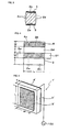
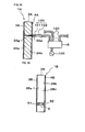
- FIG. 1 is a perspective view that shows a patch antenna device according to a first embodiment of the invention.
- FIG. 2 is a longitudinal cross-sectional view of the patch antenna device shown in FIG. 1 .
- FIG. 3 is a transverse cross-sectional view of the patch antenna device shown in FIG. 1 .
- FIG. 4 is a development of the patch antenna device shown in FIG. 1 .
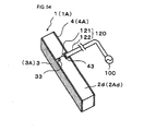
- the patch antenna device 1 of this embodiment includes a dielectric substrate 2, a first electrode 3 and a second electrode 4.
- the dielectric substrate 2 has a rectangular parallelepiped shape. Specifically, as shown in FIG. 2 , a front surface 2a and rear surface 2b of the dielectric substrate 2 face each other. As shown in FIG. 3 , a cross section taken perpendicularly to the front surface 2a and the rear surface 2b has a rectangular shape. That is, side surfaces 2c and 2d of the dielectric substrate 2 are not bulged at their centers as shown by the broken lines but are formed linearly as shown by the solid lines. As shown in FIG. 4 , the first and second electrodes 3 and 4 are provided respectively on the entire front surface 2a and entire rear surface 2b of the dielectric substrate 2.
- the width of each of the front surface 2a and rear surface 2b of the dielectric substrate 2 is equal to the width W of each of the first and second electrodes 3 and 4. Furthermore, in this embodiment, the thickness T of the dielectric substrate 2 is larger than or equal to the width W of each of the first and second electrodes 3 and 4 to thereby provide an increased thickness for the dielectric substrate 2.
- the first electrode 3 is a radiation electrode that is patterned on the front surface 2a of the dielectric substrate 2.
- the first electrode 3 is connected through a coaxial cable 120, which serves as a power supply line, to a power supply unit 100.
- the longitudinal direction (vertical direction in FIG. 1 ) of the first electrode is an excitation direction.
- holes 2g and 4a that reach the first electrode 3 are formed respectively in the dielectric substrate 2 and the second electrode 4, and an internal conductor 121 of the coaxial cable 120 is inserted into these holes 2g and 4a and connected to the first electrode 3.
- an external conductor 122 of the coaxial cable 120 is connected to the second electrode 4.
- the width W of the first electrode 3 is smaller than or equal to a quarter of the length L of the first electrode 3 that is oriented in the excitation direction.
- the second electrode 4 is a parasitic electrode that is patterned on the rear surface 2b of the dielectric substrate 2.
- the width W of the second electrode 4 is also smaller than or equal to a quarter of the length L of the second electrode 4. That is, the patch antenna device 1 of this embodiment is formed in a long slender rectangular parallelepiped shape, and is formed smaller in size than the existing square patch antenna device.
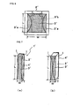
- FIG. 5 is a perspective view that shows an existing patch antenna device.
- FIG. 6 is a front view that schematically shows the existing patch antenna device and its current distribution.
- a square first electrode 3' is arranged on the front surface of a dielectric substrate 2', whereas a second electrode 4' is arranged on the rear surface of the dielectric substrate 2'. Then, when an electric power having a predetermined frequency is supplied from the power supply unit 100 to the first electrode 3', an electromagnetic wave of a predetermined resonant frequency is radiated toward the front side.
- the width W and length L of the first electrode 3' both are set to the same length and, therefore, the occupied area is large. Furthermore, as shown in FIG. 6 , an electric current at the time of excitation of the first electrode 3' concentrates on a region indicated by I adjacent to each side 3'a of the first electrode 3'. That is, as indicated by the broken line, because an electric current does not flow much adjacent to the center portion 3'b of the first electrode 3', the center portion 3'b of the first electrode 3' does not contribute to excitation and is idle. Then, the inventor studied in order to eliminate the above idle portion to miniaturize the patch antenna device. FIG.
- FIG. 7 is perspective views that illustrate the relationship between the width of an electrode and the thickness of a dielectric substrate.
- the width W of each of the first electrode 3' and the second electrode 4' is reduced to remove the region 3'b, shown in FIG. 6 , in which an electric current rarely flows, so it is possible to miniaturize the patch antenna device 1'.
- the width W of the second electrode 4' is also reduced, an electric current I distributed over the first electrode 3' is also reduced.
- a gain in the front direction decreases. Then, as shown in FIG.
- the inventor studied using the following simulation that, within which ranges the width W of the first electrode 3' and/or the thickness T of the dielectric substrate 2' are set, the volume of the patch antenna device is smaller than the existing patch antenna device and the gain is higher than or equal to the gain of the existing patch antenna device.
- FIG. 8 is a graph that shows the relationship between a width and thickness of the patch antenna device and a gain.
- FIG. 9 is a graph that shows the relationship between a width and thickness of the patch antenna device and an efficiency.
- the inventor used a dielectric substance having a relative dielectric constant of 6.4 and a dielectric loss (tan ⁇ ) of 0.002 as the dielectric substrate 2 of the patch antenna device 1, and set the length L of the dielectric substrate 2 to 80 mm. That is, the used patch antenna device 1 included the first and second electrodes 3 and 4 and the dielectric substrate 2, each having a length L of 80 mm, and then an electric power having a frequency of 910 MHz was supplied thereto.
- gains of the patch antenna device 1 were calculated through simulation while varying the width W (widths of the first and second electrodes 3 and 4 and width of the dielectric substrate 2) of the patch antenna device 1 and the thickness T (thickness of the dielectric substrate 2) of the patch antenna device 1.
- the results shown by the gain curves G1 to G4 in FIG. 8 were obtained.
- the gain curves G1, G2, G3 and G4 respectively show the relationships between the widths W for gains 1 dBi, 2 dBi, 3 dBi, and 3.5 dBi and the thickness T.
- a region J indicates a range of the width W and thickness T of the existing patch antenna device.
- a region H indicates a range of the width W and thickness T of the patch antenna device of this embodiment.
- the volume is at least about 41.6 cc.
- the patch antenna device 1 that is set to have a width W smaller than or equal to a quarter of the length 80 mm and a thickness T larger than or equal to the width W, when a gain of 3 dBi needs to be obtained, the width W just needs to be 20 mm, and the thickness T just needs to be about 20 mm.
- the volume just needs to be about 32 cc.
- the inventor used the patch antenna device 1 provided with the dielectric substrate 2 and the first and second electrodes 3 and 4 having the same relative dielectric constant, dielectric loss and length as described above, and then an electric power having a frequency of 910 MHz was supplied thereto. Then, efficiencies of the patch antenna device 1 were calculated through simulation while varying the width W and the thickness T. The results shown by efficiency curves E1 to E3 shown in FIG. 9 were obtained.
- the efficiency curves E1, E2 and E3 respectively show the relationships between a width W and a thickness T in efficiencies 70%, 80% and 90%.
- the region J in FIG. 9 in the existing patch antenna device, when the efficiency 90% needs to be obtained, it is necessary to have a width W of about 70 mm or above and a thickness T of about 10 mm.
- the volume is at least about 56 cc.
- the region H in the patch antenna device 1 that is set to have a width W smaller than or equal to a quarter of the length 80 mm and a thickness T larger than or equal to the width W, when the efficiency 90% needs to be obtained, the width W just needs to be 20 mm, and the thickness T just needs to be about 25 mm.
- the volume just needs to be at most about 40 cc. That is, it has been confirmed that in the patch antenna device 1 having the length 80 mm, when the width W is smaller than or equal to a quarter of the length and the thickness T is larger than or equal to the width W, it is possible to reduce the volume by about 29 percent or above against the volume of the existing patch antenna device while obtaining the same efficiency.
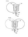
- FIG. 10 is a cross-sectional view that illustrates the function and advantageous effects of the patch antenna device 1 according to this embodiment.
- the first electrode 3 when an electric power W0 having a predetermined frequency is supplied from the power supply unit 100 through the coaxial cable 120 to the first electrode 3, the first electrode 3 operates as a radiation electrode, and the second electrode 4 connected to a grounded external conductor 122 of the coaxial cable 120 operates as a ground electrode.
- an electromagnetic wave V having a predetermined frequency, excited in the first electrode 3 is radiated toward the front side (left-hand side in FIG. 10 ).
- the width W of each of the first and second electrodes 3 and 4 is smaller than or equal to a quarter of the length L thereof, and the width of each of the front surface 2a and rear surface 2b of the dielectric substrate 2 is also equal to the width W of each of the first and second electrodes 3 and 4.
- the patch antenna device 1 may be easily mounted.
- the thickness T of the dielectric substrate 2 is larger than or equal to the width W of each of the first and second electrodes 3 and 4, there is no decrease in gain of the electromagnetic wave V radiated from the first electrode 3.
- the electromagnetic wave V having a sufficient gain is radiated in the front direction of the patch antenna device 1. In this way, according to the patch antenna device 1 of this embodiment, it is possible to obtain a high gain in the front direction while the size is small.
- FIG. 11 is a perspective view that shows a patch antenna device according to the second embodiment of the invention.
- This embodiment differs from the first embodiment in that the lengths of the first and second electrodes 3 and 4 are varied from each other.
- the length of the second electrode 4 is longer than the length (L) of the first electrode 3.
- the length L and width W of the first electrode 3 are the same as those of the first embodiment; however, the length of the second electrode 4 is longer than that of the first embodiment, and the length of the second electrode 4 is set to a length (L + L2x2) that is longer than the length L of the rear surface 2b of the dielectric substrate 2.
- both end portions 41 and 42 of the second electrode 4 are bent and arranged on both end surfaces 2e and 2f of the dielectric substrate 2.
- the dielectric substrate originally needs to have a length equal to the length of (L + L2x2) of the second electrode 4; however, with the above configuration, the dielectric substrate 2 just needs to have the length L as in the existing art.
- the patch antenna device by the amount of the lengths (L2x2) of the bent portions 41 and 42.
- the second electrode 4 that operates as the ground electrode, it is possible to reduce an electromagnetic wave that travels from the first electrode 3 toward the rear surface side (second electrode 4 side).
- the F/B ratio is increased while maintaining the miniaturized patch antenna device. As a result, it is possible to increase the gain in the front direction (in the left-hand direction of the first electrode 3).
- each of the first and second electrodes 3 and 4 has various lengths that can be matched with a load.
- the length of the second electrode 4 which matches with a load, the length of the first electrode 3 is also determined in association with the length of the second electrode 4.
- the length of the second electrode 4 which matches with a load, is not only the length of the rear surface 2b of the dielectric substrate 2 but it adds the lengths of both the end surfaces 2e and 2f and the length of the front surface 2a.
- the radiation characteristic of the patch antenna device 1 such as a gain, an F/B ratio, and a band, varies depending on the length of the second electrode 4.
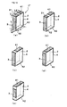
- FIG. 12 is perspective views that show variations of the length of the second electrode 4.
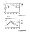
- FIG. 13 is a graph that shows the correlation between a length of the second electrode 4, and a gain, an F/B ratio, or a band.
- FIG. 12(b), FIG. 12(c), FIG. 12(d) and FIG. 12(e) respectively show the patch antenna device 1" when the overall length L + L2x2 of the second electrode 4 including the lengths of the bent portions 41 and 42 is set to 101 mm, 108 mm, 114 mm, 130 mm and 140 mm.
- the overall length L + L1x2 of the first electrode 3 including the bent portions 31 and 32 is reduced as the length of the second electrode 4 is increased.
- the band it widens as the length of the second electrode 4 is increased; by contrast, the gain and the F/B ratio decrease and, in addition, it becomes difficult to match with a load of 50 ⁇ .
- the length of the second electrode 4 there is no advantage in setting the length of the second electrode 4 so as to be 140 mm or above. From the results of the above simulations, when the dielectric substrate 2 having a relative dielectric constant of 6.4, a dielectric loss of 0.002, a length L of 80 mm, a width W of 10 mm, and a thickness T of 30 mm is used, it is desirable in terms of gain, F/B ratio and band that the length of the second electrode 4 is set within the range of 108 mm to 130 mm (modes shown in FIG. 12(b) to FIG. 12(d) ). The other configuration, function and advantageous effects are similar to those of the first embodiment, so the description thereof is omitted.
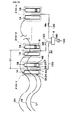
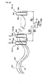
- FIG. 14 is a schematic perspective view that shows an antenna device according to a third embodiment of the invention.
- FIG. 15 is a development of a patch antenna element.
- FIG. 16 is a schematic cross-sectional view of a patch antenna element, which serves as a feeding element.
- FIG. 17 is a schematic cross-sectional view of a patch antenna element, which serves as a parasitic element.
- the antenna device 200 of this embodiment includes a pair of patch antenna elements 1A and 1B that are arranged parallel to each other at a predetermined interval D.
- the patch antenna device 1 of the first embodiment is used as the pair of patch antenna elements.
- the patch antenna element, which serves as a feeding element, and its components are assigned with reference numerals having the suffix "A”
- the patch antenna element, which serves as a parasitic element, and its components are assigned with reference numerals having the suffix "B”.
- the patch antenna devices shown in FIG. 11 and FIG. 12 may also be used as the patch antenna elements 1A and 1B.
- the patch antenna element 1A (1B) is formed so that electrodes 3A and 4A (3B and 4B) are provided respectively on a facing front surface 2Aa (2Ba) and rear surface 2Ab (2Bb) of a rectangular parallelepiped-shaped dielectric substrate 2A (2B).
- the dielectric substrate 2A (2B) has a front surface 2Aa (2Ba), a rear surface 2Ab (2Bb), side surfaces 2Ac (2Bc) and 2Ad (2Bd), and end surfaces 2Ae (2Be) and 2Af (2Bf), and electrodes 3A and 4A (3B and 4B) are respectively formed substantially over the entire faces of the front surface 2Aa (2Ba) and rear surface 2Ab (2Bb).
- the patch antenna elements 1A and 1B are arranged parallel to each other at an interval D so that the element 4A of the rear surface 2Ab of the patch antenna element 1A faces the electrode 3B of the front surface 2Ba of the patch antenna element 1B.
- a coaxial cable 120 which is extended from the power supply unit 100, is connected to the patch antenna element 1A, which is a feeding element.
- holes 2Ag and 4Aa are formed respectively in the dielectric substrate 2A and the electrode 4A so as to reach the electrode 3A of the patch antenna element 1A, and an internal conductor 121 of the coaxial cable 120 is inserted through the holes 2Ag and 4Aa and connected to the electrode 3A.
- an external conductor 122 of the coaxial cable 120 is connected to the electrode 4A.
- a reactance circuit 5 is connected between the front surface-side electrode and the rear surface-side electrode.
- holes 2Bg and 4Ba are formed respectively in the dielectric substrate 2B and the electrode 4B so as to reach the electrode 3B of the patch antenna element 1B, and a conductor wire 130 is inserted through the holes 2Bg and 4Ba.
- one end of the conductor wire 130 is connected to the electrode 3B, and the other end thereof is connected to an input end of the reactance circuit 5.
- an output end of the reactance circuit 5 is connected to the conductor wire 131, while the conductor wire 131 is connected to the grounded rear surface-side electrode 4B.
- the patch antenna elements 1A and 1B have the same shape, and the width of each of the electrodes 3A and 3B (4A and 4B) is shorter than the length L. That is, both the patch antenna elements 1A and 1B each are formed into a long slender quadrangular prism in order to reduce in size in the width direction as compared with a typical square cylinder element.
- the patch antenna element 1B which is the feeding element, is arranged on a side opposite to a radiation direction of the patch antenna element 1A. Specifically, the antenna device 200 sets the radiation direction of an electromagnetic wave to the electrode 3A side of the patch antenna element 1A.
- the patch antenna element 1B is arranged on a side opposite to a radiation direction of an electromagnetic wave from the patch antenna element 1A, that is, arranged at the interval D on the right-hand side of the patch antenna element 1A in FIG. 14 . Then, the interval D between the patch antenna elements 1A and 1B is set within the range of 0.12 times to 0.30 times a free space wavelength at the working frequency of a UHF band.
- FIG. 18 is a schematic side view that illustrates the function and advantageous effects of the antenna device 200 according to this embodiment.
- a signal having a predetermined frequency is supplied from the power supply unit 100 through the coaxial cable 120 to the patch antenna element 1A
- the patch antenna element 1A is excited, and as shown by the solid line, an electromagnetic wave V2 having a predetermined frequency is radiated from the electrodes 3A and 4A of the patch antenna element 1A toward the front side and rear side of the patch antenna element 1A.
- the electromagnetic wave V2 radiated from the electrode 4A side is electromagnetically coupled with the patch antenna element 1B, and then the patch antenna element 1B resonates at the predetermined frequency.
- the patch antenna element 1B radiates an electromagnetic wave V3 from the electrodes 3B and 4B toward the front side and rear side of the patch antenna element 1B.
- the phase and/or amplitude of the electromagnetic wave V3 may be adjusted by appropriately setting the reactance value of the reactance circuit 5 of the patch antenna element 1B and the element interval D between the patch antenna elements 1A and 1B.
- FIG. 19 is a correlation graph between an element interval D and a gain.
- FIG. 20 is a correlation graph between an element interval D and an F/B ratio.
- the patch antenna elements 1A and 1B were configured so that the dielectric substrates 2A and 2B each have a relative dielectric constant of 6.4, a width W of 15 mm, a length L of 80 mm, and a thickness T of 15 mm, and then a signal having a frequency of 920 MHz was supplied from the power supply unit 100 to the patch antenna element 1A. Then, while varying the element interval D between the patch antenna elements 1A and 1B, the gain and the F/B ratio were analyzed for each element interval D.
- the relative dielectric constant of each of the dielectric substrates 2A and 2B was changed to miniaturize the patch antenna elements 1A and 1B. Specifically, the relative dielectric constant of each of the dielectric substrates 2A and 2B was set to 21, the width W, length L and thickness T of each of the patch antenna elements 1A and 1B were respectively set to 10 mm, 55 mm and 15 mm, and then the test similar to the above test was conducted. As shown by the curve S5 in FIG. 19 , when the element interval D ranges from 0.12 times to 0.30 times the wavelength, a gain higher than or equal to about 4 dB may be obtained, and as shown by the curve S5 in FIG. 20 , an F/B ratio larger than or equal to about 6 dB may be obtained.
- the relative dielectric constant of each of the dielectric substrates 2A and 2B is increased to 38, the width W, length L and thickness T of each of the patch antenna elements 1A and 1B were respectively set to 10 mm, 40 mm and 15 mm, and then the test similar to the above test was conducted.
- the curve S6 in FIG. 19 when the element interval D ranges from 0.12 times to 0.30 times the wavelength, a gain higher than or equal to about 3 dB may be obtained, and as shown by the curve S6 in FIG. 20 , an F/B ratio larger than or equal to about 5 dB may be obtained.
- the antenna device 200 of this embodiment when the element interval D between the patch antenna elements 1A and 1B is set within the range of 0.12 times to 0.30 times the wavelength at the working frequency, a gain higher than or equal to about 3 dB and an F/B ratio larger than or equal to about 5 dB may be obtained even when the microminiaturized patch antenna elements 1A and 1B having a length of 40 mm are used.
- FIG. 21 is a correlation graph between a reactance and an element interval D, and a gain.
- FIG. 22 is a correlation graph between a reactance and an element interval D, and an F/B ratio.
- the patch antenna elements 1A and 1B were configured so that the dielectric substrates 2A and 2B each have a relative dielectric constant of 6.4, a width W of 15 mm, a length L of 80 mm, and a thickness T of 15 mm, and then a signal having a frequency of 920 MHz was supplied from the power supply unit 100 to the patch antenna element 1A. Then, while varying the reactance of the reactance circuit 5 of the patch antenna element 1B, the gain and the F/B ratio were analyzed for each element interval D. Then, the results shown by the curved surfaces Sg and Sfb in FIG. 21 and FIG. 22 were obtained. As is apparent from the curved surface Sg in FIG.
- the antenna device 200 of this embodiment while the antenna device 200 is small, it is possible to obtain a high gain in the front direction and a large F/B ratio.
- the patch antenna elements 1A and 1B are used as elements, it is easy to match with an unbalanced circuit, such as a coaxial line. Thus, it is possible to efficiently supply a signal from the power supply unit 100 to the antenna device 200.
- the patch antenna element 1B serves as a non-power supplied parasitic element.
- the structure in comparison with an antenna that uses both the patch antenna elements 1A and 1B as driven elements, the structure is simple because a distribution circuit for a signal, or the like, is unnecessary. Hence, it is possible to reduce the cost of the antenna device 200.
- the other configuration, function and advantageous effects are similar to those of the first and second embodiments, so the description thereof is omitted.
- FIG. 23 is a schematic diagram that shows the configuration of an antenna device according to a fourth embodiment of the invention.
- FIG. 24 is a perspective view that shows the configuration of each sub-array unit.
- FIG. 25 is a schematic cross-sectional view of a first patch antenna element.
- an antenna device 201 of this embodiment includes n (n is integer larger than or equal to 2) sub-array units 210-1 to 210-n, and a distributor 6 for outputting an electric power from a power supply unit 100 to the sub-array units 210-1 to 210-n with a predetermined phase difference.
- each sub-array unit 210-1 (210-2 to 210-n) is formed of a first patch antenna element 1A, which is a feeding element placed on a front side, and a second patch antenna element 1B, which is a parasitic element placed on a rear side. That is, in this embodiment, the pair of patch antenna elements 1A and 1B used in the above third embodiment serve as the first patch antenna element 1A and the second patch antenna element 1B that constitute each sub-array unit 210-1 (210-2 to 210-n).
- the first patch antenna element 1A is formed of a dielectric substrate 2A, a first electrode 3A and a second electrode 4A.
- the first electrode 3A and the second electrode 4A are formed respectively on the facing front face 2Aa and rear face 2Ab of the rectangular parallelepiped-shaped dielectric substrate 2A.
- a coaxial cable 120 is extended from the power supply unit 100 through the distributor 6 and connected to each first patch antenna element 1A.
- each second patch antenna element 1B which is a parasitic element, is formed of a dielectric substrate 2B, a first electrode 3B and a second electrode 4B.
- the first electrode 3B and the second electrode 4B are formed respectively on the facing front face 2Ba and rear face 2Bb of the rectangular parallelepiped-shaped dielectric substrate 2B.
- a reactance circuit 5 is connected to a side surface 2Bd side of the second patch antenna element 1B. By so doing, it is possible to adjust the reactance of the entire second patch antenna element 1B by the reactance circuit 5.
- FIG. 26 is a side view of the second patch antenna element 1B.
- the reactance circuit 5 may employ various circuits.
- a discrete inductor, a discrete capacitor, a series resonant circuit or parallel resonant circuit formed of an inductor and a capacitor, a circuit in which an inductor or a capacitor is connected in series with these resonant circuit, a circuit that uses a variable capacitance element, such as a varactor, in place of a capacitor, or the like, may be employed.
- the reactance circuit 5 employs an inductor. Specifically, as shown in FIG.
- extended portions 51 and 52 of the first and second electrodes 3B and 4B of the second patch antenna element 1B are formed on the side surface 2Bd of the dielectric substrate 2B, and both ends of an inductor component 5 are connected respectively to the extended portions 51 and 52.
- the inductor may be not only formed of the chip component-like inductor component 5 but also formed of an electrode.
- a meander-shaped electrode 5' having an appropriate length may be patterned on the side surface 2Bd of the dielectric substrate 2B, and both ends of the electrode may be connected to the first and second electrodes 3B and 4B.
- the first patch antenna element 1A is arranged so as to be located in front of the second patch antenna element 1B.
- the first and second patch antenna elements 1A and 1B are arranged parallel to each other at an interval D, the second electrode 4A of the first patch antenna element 1A located on the front side faces the first electrode 3B of the second patch antenna element 1B located on the rear side.
- FIG. 28 is a schematic side view that illustrates radio wave radiation of each sub-array unit 210-1 (210-2 to 210-n).
- an electric power W1 (W2 to Wn) having a predetermined frequency is supplied from the power supply unit 100 through the distributor 6 and the coaxial cable 120 to the first patch antenna element 1A of each sub-array unit 210-1 (210-2 to 210-n), as shown by the solid line in FIG. 28 , a radio wave V2 having a predetermined frequency is radiated frontward and rearward from the first electrode 3A of the first patch antenna element 1A.
- the radio wave V2 radiated from the second electrode 4A side of the first patch antenna element 1A is electromagnetically coupled with the second patch antenna element 1B, and the second patch antenna element 1B resonates at the predetermined frequency.
- the second patch antenna element 1B radiates a radio wave V3 from the first and second electrodes 3B and 4B in the front direction and rear direction of the second patch antenna element 1B.
- the reactance circuit 5 by appropriately adjusting the phase and/or amplitude of the radio wave V3 using the reactance circuit 5, it is possible to make the radio wave V3, traveling toward the rear side of the second patch antenna element 1B, interfere with the radio wave V2 from the first patch antenna element 1A to suppress the radio wave.
- each sub-array unit 210-1 (210-2 to 210-n), as shown by the alternate long and two short dashed lines, it is possible to radiate a composite radio wave U1 (U2 to Un) of the radio waves V2 and V3, having a high gain, toward the front side (in the left-hand direction in FIG. 28 ) of each sub-array unit 210-1 (210-2 to 210-n).
- the n sub-array units 210-1 to 210-n are arranged in a line at intervals D1
- the second electrode 4B of the second patch antenna element 1B of the preceding sub-array unit 210-m (1 ⁇ m ⁇ n) is arranged so as to face the first electrode 3A of the first patch antenna element 1A of the subsequent sub-array unit 210-(m+1). That is, the radio wave radiation direction of each of the sub-array units 210-1 to 210-n is oriented toward the front side (left-hand side in FIG. 23 ).
- the interval D1 between the preceding sub-array unit 210-m and the subsequent sub-array unit 210-(m+1) is set to substantially half the free space wavelength at the working frequency. Specifically, the interval D1 is set to half the wavelength at the frequency of the electric power W0 supplied from the power supply unit 100.
- the distributor 6 is a known distributor, and gives a predetermined phase difference to the electric power W0 supplied from the power supply unit 100 and distributes the electric powers W1 to Wn, whose phases are deviated, respectively to the sub-array units 210-1 to 210-n. Specifically, the distributor 6 operates so that a phase difference between electric powers Wm and Wm+1 supplied respectively to the preceding sub-array unit 210-m and the subsequent sub-array unit 210-(m+1) is 180°. In addition, the distributor 6 operates so that the electric power Wm+1 supplied to the subsequent sub-array unit 210-(m+1) advances by a phase difference of 180° from the electric power Wm supplied to the preceding sub-array unit 210-m. Thus, the phase of a radio wave radiated from the subsequent sub-array unit 210-(m+1) advances by 180° from the phase of a radio wave radiated from the preceding sub-array unit 210-m.
- FIG. 29 is a schematic diagram that illustrates the function and advantageous effects of the antenna device.
- electric powers W1 to Wn sequentially having a phase difference of 180° are generated by the distributor 6, and these electric powers W1 to Wn are respectively supplied to the first patch antenna elements 1A of the sub-array units 210-1 to 210-n.
- the radio wave Un indicated by the alternate long and two short dashed lines is radiated from the last sub-array unit 210-n, and the radio wave Un-1 is radiated from the preceding sub-array unit 210-(n-1) with the phase delayed by 180° from the radio wave Un.
- the radio wave U2 indicated by the alternate long and short dashed line is radiated from the sub-array unit 210-2 with the phase delayed by 180° ⁇ (n-2) from the radio wave Un
- the radio wave U1 shown by the solid line is radiated from the sub-array unit 210-1 with the phase delayed by 180° ⁇ (n-1) from the radio wave Un.
- the interval D1 between the adjacent sub-array units 210-m and 210-(m+1) is set to half the wavelength of the radio wave U1 (U2 to Un) radiated from the sub-array unit 210-1 (210-2 to 210-n)
- all the radio waves U1 to Un radiated in the front direction of the sub-array unit 210-1 coincide with one another.
- the radio waves U1 to Un are superimposed, and the gain of a radio wave radiated from the antenna device 201 increases in association with the number n of sub-array units.
- FIG. 30 is a correlation graph between the number of patch antenna elements and a gain.
- the patch antenna elements were configured so that the dielectric substrates 2A and 2B each have a relative dielectric constant of 6.4, a width W of 15 mm, a length L of 80 mm and a thickness T of 15 mm (see FIG. 24 ), and then an electric power having a frequency of 920 MHz was supplied to the patch antenna element. Then, the number of patch antenna elements was varied, and the gain was analyzed for each number of elements. The results shown in FIG. 30 were obtained.
- the gain when the number of elements is "1" is a gain when only the first patch antenna element 1A was simulated without the second patch antenna element 1B, which serves as a parasitic element, accompanied therewith;
- the number of elements "2" indicates a gain when the first and second patch antenna elements 1A and 1B that constitute each sub-array unit were simulated;
- the number of elements "4" indicates a gain when two sub-array units, each of which is formed of the first and second patch antenna elements 1A and 1B, were arranged in a line and simulated;
- the number of elements "8" indicates a gain when four sub-array units were arranged in a line and simulated.
- the gain when the number of patch antenna elements doubles, the gain also increases by about 3 dBi.
- the gain may be increased in association with the number n of sub-array units.
- the antenna device 201 of this embodiment because the gain of the radio wave may be increased in association with the number of sub-array units and/or the number of patch antenna elements, it is possible to implement the antenna device that radiates a radio wave with a high gain. Furthermore, because the first and second patch antenna elements 1A and 1B are arranged in a line in the radiation direction of the radio wave, it is possible to implement the miniaturized antenna device 201 by suppressing the area in the planar direction. As a result, it is possible to easily mount the antenna device 201 of this embodiment on an electronic device having a narrow antenna mounting area as well.
- the patch antenna elements 1A and 1B are used as components, it is easy to match with an unbalanced circuit, such as a coaxial line and, therefore, it is possible to efficiently supply an electric power from the power supply unit 100 to the antenna device 201.
- the other configuration, function and advantageous effects are similar to those of the first to third embodiments, so the description thereof is omitted.
- FIG. 31 is a schematic perspective view that shows an antenna device according to a fifth embodiment of the invention.
- FIG. 32 is a schematic cross-sectional view of each patch antenna element.
- the antenna device 202 of this embodiment includes a pair of patch antenna elements 1A and 1A' that are arranged parallel to each other at a predetermined interval D.
- the patch antenna element 1A (1A') is the patch antenna device 1 of the first embodiment, and is a feeding element such that electrodes 3A and 4A (3A' and 4A') are provided respectively on an opposite front surface 2Aa (2Aa') and rear surface 2Ab (2Ab') of a rectangular parallelepiped-shaped dielectric substrate 2A (2A').
- the patch antenna elements 1A and 1A' are arranged parallel to each other at the interval D so that the electrode 4A of the rear surface 2Ab of the patch antenna element 1A faces the electrode 3A' of the front surface 2Aa' of the patch antenna element 1A', and coaxial cables 120 and 120' of the patch antenna elements 1A and 1A' are connected through a distributor 6 to a power supply unit 100.
- the coaxial cable 120 (120') is extended from the distributor 6 and connected to the patch antenna element 1A (1A').
- the above patch antenna elements 1A and 1A' have the same shape, and the width W of each of the electrodes 3A and 3A' (4A and 4A') is shorter than the length L. That is, both the patch antenna elements 1A and 1A' each are formed into a long slender quadrangular prism in order to reduce in size in the width direction as compared with a typical square element.
- the distributor 6 distributes an electric power W0 having a predetermined frequency, supplied from the power supply unit 100, to electric powers W1 and W2 and supplies the electric powers W1 and W2 to the patch antenna elements 1A and 1A'.
- the distributor 6, when distributing, has a function to output the electric powers W1 and W2 by providing a difference between the phase of the electric power W1 and the phase of the electric power W2.
- the phase difference between the electric powers W1 and W2 ranges from 60 degrees to 120 degrees. Note that when a distributor has no function to output by providing a phase difference, by varying the lengths of the coaxial cables 120 and 120' to the elements, it is possible to provide the above phase difference.
- the distributor 6 may select not only the one that equalizes a distribution ratio of the electric power W1 and a distribution ratio of the electric power W2 but also the one that makes the distribution ratio unequal. However, in this embodiment, the selected distributor 6 sets a distribution ratio of the electric power W1 to the electric power W2 so that the amplitude of a radio wave radiated from one of the patch antenna elements 1A and 1A' is higher by a value ranging from 2 dB to 6dB than the amplitude of a radio wave radiated from the other one.
- the above distributor 6 is a known circuit, and, for example, from among a 90-degree hybrid coupler, a combining T, a delay line, or the like, a circuit whose output-side distribution ratio is appropriately set is employed.
- FIG. 33 is a schematic side view that illustrates the function and advantageous effects of the antenna device 202 according to this embodiment.
- the electric power W0 having a predetermined frequency is supplied from the power supply unit 100
- the electric power W1 and the electric power W2, distributed by the distributor 6 are respectively supplied through the coaxial cables 120 and 120' to the patch antenna elements 1A and 1A'.
- the patch antenna elements 1A and 1A' both are excited, and as shown in the solid line, a radio wave V2 having a predetermined frequency is radiated from the electrodes 3A and 4A of the patch antenna element 1A toward the front side and rear side of the patch antenna element 1A, and as shown by the broken line, a radio wave V3 having a predetermined frequency is radiated from the electrodes 3A' and 4A' of the patch antenna element 1A' toward the front side and rear side of the patch antenna element 1A'.
- a radio wave V2 having a predetermined frequency is radiated from the electrodes 3A' and 4A' of the patch antenna element 1A' toward the front side and rear side of the patch antenna element 1A'.
- the distributor 6 is selected so that the phase of the electric power W1 supplied to the patch antenna element 1A is delayed by 60 degrees to 120 degrees from the phase of the electric power W2 supplied to the patch antenna element 1A'.
- the radio wave V2 traveling toward the front side of the patch antenna element 1A is amplified by the radio wave V3 from the patch antenna element 1A', and the gain in the front direction of the antenna device 202 increases.
- the radio wave V3 traveling toward the rear side of the patch antenna element 1A' interferes with the radio wave V2 of the rear side of the patch antenna element 1A and is suppressed, so the F/B ratio of the antenna device 202 increases.
- the distributor 6 is selected so as to have a distribution ratio such that the amplitude of the radio wave V2 from the patch antenna element 1A is larger than the amplitude of the radio wave V3 from the patch antenna element 1A'.
- the distributor 6 is selected so that the phase of the electric power W2 supplied to the patch antenna element 1A' is delayed by 60 degrees to 120 degrees from the phase of the electric power W1 supplied to the patch antenna element 1A.
- the radio wave V3 traveling toward the rear side of the patch antenna element 1A' is amplified by the radio wave V2 from the patch antenna element 1A, and the gain in the rear direction of the antenna device 202 increases.
- the radio wave V2 traveling toward the front side of the patch antenna element 1A interferes with the radio wave V3 of the front side of the patch antenna element 1A' and is suppressed, so the F/B ratio of the antenna device 202 increases.
- the distributor 6 is selected so as to have a distribution ratio such that the amplitude of the radio wave V3 from the patch antenna element 1A' is larger than the amplitude of the radio wave V2 from the patch antenna element 1A.
- the distributor 6 having the above distribution ratio and phase difference is selected; however, when a distributor that is able to vary these distribution ratio and phase difference is used, it is not only possible to improve a gain and/or an F/B ratio without replacing the distributor 6 but also possible to selectively change the directivity of the antenna device 202.
- FIG. 34 is a correlation graph between a phase difference and an amplitude ratio, and a gain.
- FIG. 35 is a correlation graph between a phase difference and an amplitude ratio, and an F/B ratio.
- the patch antenna elements 1A and 1A' were configured so that the dielectric substrates 2A and 2A' each have a relative dielectric constant of 6.4, a width W of 15 mm, a length L of 80 mm and a thickness T of 15 mm, and arranged at an element interval D of 60 mm, and then an electric power having a frequency of 900 MHz was supplied from the power supply unit 100 to the patch antenna elements 1A and 1A'. Then, while varying the phase difference of the electric power W1 of the patch antenna element 1A against the electric power W2 of the patch antenna element 1A', the gain and the F/B ratio were analyzed for each amplitude ratio. The results are shown by the curved surfaces Sg and Sfb in FIG. 34 and FIG.
- the gain and F/B ratio higher than or equal to 6 dB may be obtained.
- the gain is about 3 to 4 dB, whereas in the antenna device 202 of this embodiment, it is possible to obtain a gain higher by about 2 dB with the same size.
- the antenna device 202 of this embodiment while the antenna device 202 is small, it is possible to obtain a high gain in the front direction and a large F/B ratio.
- the patch antenna elements 1A and 1A' are used as elements, it is easy to match with an unbalanced circuit, such as a coaxial line.
- an unbalanced circuit such as a coaxial line.
- the other configuration, function and advantageous effects are similar to those of the first to fourth embodiments, so the description thereof is omitted.
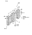
- FIG. 36 is a schematic diagram that shows the configuration of an antenna device according to the sixth embodiment of the invention.
- FIG. 37 is a perspective view that shows the configuration of the antenna device.
- the antenna device 203 of this embodiment includes n (n is integer larger than or equal to 2) patch antenna elements 1A-1 to 1A-n, and a distributor 6 for outputting an electric power from a power supply unit 100 to the patch antenna elements 1A-1 to 1A-n with a predetermined phase difference.
- Each patch antenna element 1A-1 (1A-2 to 1A-n) is a feeding element, and, as shown in FIG. 37 , has the same structure as the first patch antenna element 1A that is employed in the fourth embodiment. That is, each patch antenna element 1A-1 (1A-2 to 1A-n) is formed of a dielectric substrate 2A, a first electrode 3A and a second electrode 4A, and is connected to a coaxial cable 120 that is extended from the power supply unit 100 through the distributor 6.
- the first electrode 3A and the second electrode 4A are formed respectively on the facing front face 2Aa and rear face 2Ab of the rectangular parallelepiped-shaped dielectric substrate 2A.
- the n patch antenna elements 1A-1 to 1A-n are arranged in a line at intervals D, and the subsequent patch antenna element 1A-(m+1) is located behind the preceding patch antenna element 1A-m (1 ⁇ m ⁇ n). That is, the second electrode 4A of the preceding patch antenna element 1A-m (1 ⁇ m ⁇ n) is arranged so as to face the first electrode 3A of the subsequent patch antenna element 1A-(m+1), and the radio wave radiation direction of each of the patch antenna elements 1A-1 to 1A-n is oriented in the front direction (left-hand side in FIG. 36 ). Then, the interval D between the preceding patch antenna element 1A-m and the subsequent patch antenna element 1A-(m+1) is set to substantially a quarter of the free space wavelength at the working frequency.
- the distributor 6 is a known distributor. This distributor 6 operates so that the phase difference between the electric powers Wm and Wm+1 respectively supplied to the preceding and subsequent patch antenna elements 1A-m and 1A-(m+1) becomes 90°. In addition, the distributor 6 operates so that the electric power Wm+1 supplied to the subsequent patch antenna element 1A-(m+1) advances by a phase difference of 90° from the electric power Wm supplied to the preceding patch antenna element 1A-m. Thus, the phase of a radio wave radiated from the subsequent patch antenna element 1A-(m+1) advances by 90° from the phase of a radio wave radiated from the preceding patch antenna element 1A-m.
- FIG. 38 is a schematic diagram that illustrates the function and advantageous effects of the antenna device.
- an electric power W0 is output from the power supply unit 100
- electric powers W1 to Wn having a phase difference of 90° are generated by the distributor 6, and these electric powers W1 to Wn are respectively supplied to the patch antenna elements 1A-1 to 1A-n.
- the radio wave Un' indicated by the alternate long and two short dashed lines is radiated from the last patch antenna element 1A-n
- the radio wave Un-1' is radiated from the preceding patch antenna element 1A-(n-1) with the phase delayed by 90° from the radio wave Un'.
- the radio wave U2' indicated by the alternate long and short dashed line is radiated from the patch antenna element 1A-2 with the phase delayed by 90° ⁇ (n-2) from the radio wave Un'
- the radio wave U1' shown by the solid line is radiated from the patch antenna element 1A-1 with the phase delayed by 90° ⁇ (n-1) from the radio wave Un'.
- the interval D between the adjacent patch antenna elements 1A-m and 1A-(m+1) is set to a quarter of the wavelength of each of the radio waves U1' to Un' radiated from the patch antenna elements 1A-1 to 1A-n, all the radio waves U1' to Un' radiated in the front direction of the patch antenna element 1A-1 coincide with one another.
- the gain of a radio wave radiated from the antenna device 203 increases in association with the number n of patch antenna elements.
- FIG. 39 is a correlation graph between the number of elements and a gain.
- the patch antenna elements were configured so that the dielectric substrates 2A each have a relative dielectric constant of 6.4, a width W of 15 mm, a length L of 80 mm and a thickness T of 15 mm, and then an electric power having a frequency of 920 MHz was supplied to the patch antenna elements. Then, the number of patch antenna elements was varied, and the gain was analyzed for each number of elements. The results shown in FIG. 39 were obtained. As is apparent from the results shown in FIG.
- the gain may be increased in association with the number n of patch antenna elements.
- the other configuration, function and advantageous effects are similar to those of the fourth embodiment, so the description thereof is omitted.
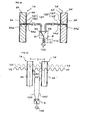
- FIG. 40 is a schematic perspective view that shows an antenna device according to a seventh embodiment of the invention.
- FIG. 41 is a schematic cross-sectional view that shows a state of connection among each patch antenna element, a change-over switch 6 and a power supply unit 100.
- the antenna device 204 of this embodiment includes a pair of patch antenna elements 1A and 1A' arranged parallel to each other at a predetermined interval D; and the change-over switch 6.
- the patch antenna elements 1A and 1A' are arranged parallel to each other at the interval D so that an electrode 4A of a rear surface 2Ab of the patch antenna element 1A faces an electrode 4A' of a rear surface 2Ab' of the patch antenna element 1A', and coaxial cables 120 and 120' of the patch antenna elements 1A and 1A' are connected through the change-over switch 6 to the power supply unit 100.
- these patch antenna elements 1A and 1A' have the same shape, and the width W of each of the electrodes 3A and 3A' (4A and 4A') is shorter than the length L. That is, both the patch antenna elements 1A and 1A' each are formed into a long slender quadrangular prism in order to reduce in size in the width direction as compared with a typical square element.
- the coaxial cables 120 and 120' are respectively extended from these patch antenna elements 1A and 1A', and these coaxial cables 120 and 120' are connected through the change-over switch 6 to the power supply unit 100.
- the change-over switch 6 has a movable contact 61 and a pair of fixed contacts 62 and 63. Then, the movable contact 61 is connected to an internal conductor 111 of a coaxial cable 110 extended from the power supply unit 100, and the fixed contacts 62 and 63 are connected to internal conductors 121 and 121' of the respective coaxial cables 120 and 120'.
- the patch antenna element 1A serves as a feeding element
- the patch antenna element 1A' serves as a parasitic element.
- the patch antenna element 1A serves as a parasitic element
- the patch antenna element 1A' serves as a feeding element.
- FIG. 42 is a schematic side view that illustrates the function and advantageous effects of the antenna device 204 according to this embodiment.
- FIG. 43 is a schematic side view that shows the directivity when the left-hand side patch antenna element 1A serves as a feeding element.
- FIG. 44 is a schematic side view that shows the directivity when the right-hand side patch antenna element 1A' serves as a feeding element. As shown by the solid line in FIG.
- the patch antenna element 1A serves as a feeding element and is excited.
- the radio wave V2 shown by the solid line is radiated from the electrodes 3A and 4A of the patch antenna element 1A toward the front side and rear side of the patch antenna element 1A.
- the patch antenna element 1A' serves as a parasitic element, and resonates with the radio wave V2 from the patch antenna element 1A.
- the radio wave V3 indicated by the broken line is radiated from the electrodes 3A' and 4A' of the patch antenna element 1A' toward the front side and rear side of the patch antenna element 1A'.
- the patch antenna element 1A and the patch antenna element 1A' resonate with each other so as to have the same phase in the front direction (left-hand direction in FIG. 42 ) and, as a result, the gain of the antenna device 204 in the front direction increases.
- the radio wave V3 traveling toward the rear side (right-hand side in FIG.
- the patch antenna element 1A' operates as a reflector to increase the gain of a radio wave in the left-hand direction of the antenna device 204 and the F/B ratio of the antenna device 204.
- the directivity of the antenna device 204 is biased in the left-hand direction.
- the patch antenna element 1A serves as a parasitic element and resonates with the radio wave V3 from the patch antenna element 1A', and then the radio wave V2 indicated by the solid line is radiated from the electrodes 3A and 4A of the patch antenna element 1A toward the front side and rear side of the patch antenna element 1A.
- the patch antenna element 1A and the patch antenna element 1A' resonate with each other so as to have the same phase in the rear direction and, as a result, the gain of the antenna device 204 in the rear direction increases.
- the radio wave V2 traveling toward the front side of the patch antenna element 1A is suppressed. That is, when the change-over switch 6 is changed, the patch antenna element 1A operates as a reflector to increase the gain of a radio wave in the right-hand direction of the antenna device 204 and the F/B ratio of the antenna device 204. As a result, as shown in FIG. 44 , the directivity of the antenna device 204 is changed in the right-hand direction.
- the antenna device 204 of this embodiment it is possible to obtain a high gain in the front direction or in the rear direction and a large F/B ratio while the size is small, and it is possible to easily change the directivity.
- the patch antenna elements 1A and 1A' are used as elements, it is easy to match with an unbalanced circuit, such as a coaxial line. Thus, it is possible to efficiently supply a signal from the power supply unit 100 to the antenna device 204.
- the electrode 3A (3A') of the patch antenna element 1A (1A') is regarded as an antenna electrode
- the electrode 4A (4A') is regarded as a ground electrode
- the electrode 3A (3A') is oriented toward the front side, which is the radiation direction
- the electrode 4A (4A') is oriented toward the rear side.
- the electrodes 3A and 4A (3A' and 4A') have substantially the same size, it is difficult to clearly identify which is the ground electrode and which is the antenna electrode. Then, even when which one serves as the ground electrode and the other one serves as the antenna electrode, there is no large difference in antenna characteristic.
- the similar function and advantageous effects to those of the antenna device 204 of the above embodiment are obtained. That is, even when the patch antenna element 1A' is oriented reversely with respect to the embodiment as shown in FIG. 45(a) , or even when the patch antenna element 1A is oriented reversely with respect to the embodiment as shown in FIG. 45(b) , the similar characteristic to that of the antenna device 204 of the embodiment may be achieved.
- the other configuration, function and advantageous effects are similar to those of the first to sixth embodiments, so the description thereof is omitted.
- FIG. 46 is a schematic perspective view that shows an antenna device according to the eighth embodiment of the invention.
- FIG. 47 is a schematic cross-sectional view that shows a patch antenna element, which serves as a parasitic element.
- the antenna device 205 of this embodiment includes three patch antenna elements 1B-1, 1A, and 1B-2. These patch antenna elements 1B-1, 1A, and 1B-2 are arranged parallel to one another at predetermined intervals D so that electrodes 4A and 3B (4B and 3A) of the adjacent patch antenna elements 1A and 1B-1 (1B-2 and 1A) face each other.
- the middle patch antenna element 1A serves as a feeding element that is connected to a power supply unit 100, and the patch antenna elements 1B-1 and 1B-2 located at both sides serve as parasitic elements, each having a variable reactance circuit 5.
- the patch antenna element 1A is directly connected to the power supply unit 100 through a coaxial cable 120.
- the variable reactance circuits 5 are respectively connected to the patch antenna elements 1B-1 and 1B-2, which serve as parasitic elements, and are terminated. Specifically, as shown in FIG. 47 , holes 2Bg and 4Ba are formed respectively in the dielectric substrate 2B and the electrode 4B so as to reach the electrode 3B of each patch antenna element 1B-1 (1B-2), and a conductor wire 140 is inserted through the holes 2Bg and 4Ba. Thus, one end of the conductor wire 140 is connected to the electrode 3B, and the other end thereof is connected to an input end of the variable reactance circuit 5. Then, an output end of the variable reactance circuit 5 is connected to a conductor wire 141, while the conductor wire 141 is connected to the electrode 4B.
- the variable reactance circuit 5 may employ any known variable reactance circuits.
- the variable reactance circuit 5 is formed of a variable capacitance diode. Specifically, a variable capacitance diode 53 and an inductor 54 are serially connected. The cathode side of the variable capacitance diode 53 is connected to the conductor wire 140, and one end of the inductor 54 is connected to the conductor wire 141.
- Vcc direct-current voltage
- FIG. 48 is a schematic side view that illustrates the function and advantageous effects of the antenna device 205 according to this embodiment.
- FIG. 49 is a schematic side view that shows the directivity of the antenna device 205.
- a signal having a predetermined frequency is supplied from the power supply unit 100 through the coaxial cable 120 to the patch antenna element 1A, and the variable reactance circuit 5 of the patch antenna element 1B-1 is adjusted to an inductive reactance, while the variable reactance circuit 5 of the patch antenna element 1B-2 is adjusted to a capacitive reactance.
- the patch antenna element 1B-1 serves as a reflector, the radio wave V2 traveling toward the rear side (right-hand direction in FIG. 48 ) of the patch antenna element 1A is suppressed, and the radio wave V2 traveling toward the front side (left-hand direction in FIG. 48 ) of the patch antenna element 1A increases.
- the gain of a radio wave in the front direction of the antenna device 205 increases, and the F/B ratio increases, and then the directivity shown by the solid line in FIG. 49 is obtained.
- variable reactance circuit 5 of the patch antenna element 1B-1 is adjusted to a capacitive reactance
- variable reactance circuit 5 of the patch antenna element 1B-2 is adjusted to an inductive reactance
- the patch antenna element 1B-2 serves as a reflector
- the antenna device 205 exhibits the directivity shown by the broken line in FIG. 49 .
- the antenna device 205 of this embodiment while the antenna device 205 is small, it is not only possible to obtain a high gain in the front direction and a large F/B ratio but also possible to easily change the directivity of the antenna device 205 by the variable reactance circuits 5 of the patch antenna elements 1B-1 and 1B-2.
- the other configuration, function and advantageous effects are similar to those of the first to seventh embodiments, so the description thereof is omitted.
- FIG. 50 is a cross-sectional view that shows a relevant part of an antenna device according to the ninth embodiment of the invention.
- the variable reactance circuits 5 of the patch antenna elements 1B-1 and 1B-2 are configured as the variable capacitance diode 53 and the inductor 54, and the reactances of the variable reactance circuits 5 may be continuously varied.
- a variable reactance circuit 5" which is able to discretely vary the reactance, is employed.
- the variable reactance circuit 5" includes a change-over switch 55 and a plurality of fixed reactance circuits 56 to 59 having different reactances.
- any of the fixed reactance circuits 56 to 59 is connected to the patch antenna element 1B-1 (1B-2), thus making it possible to vary the reactance of the variable reactance circuit 5".
- the other configuration, function and advantageous effects are similar to those of the second embodiment, so the description thereof is omitted.
- the overall length of the electrode 4 is equal or increased against the electrode 3 that is formed over the entire front surface 2a of the dielectric substrate 2.
- the scope of the invention encompasses the patch antenna device, as shown in FIG. 51 , in which the first electrode 3, whose length L is shorter than the length of the front surface 2a of the dielectric substrate 2, is formed on the front surface 2a, and the overall length of the second electrode 4 is longer than the first electrode 3.
- the electrode 4 is longer than the electrode 3, and the both end portions 41 and 42 are arranged so as to be bent onto the end surfaces 2e and 2f of the dielectric substrate 2.
- the length of at least one of the electrodes 3 and 4 may be longer than the length of each of the front surface 2a and rear surface 2b of the dielectric substrate 2, and that electrode may be arranged so as to be bent onto the end surfaces 2e and 2f.
- the scope of the invention also encompasses the invention in which the electrode 3 is longer than the electrode 4 and the end portion thereof is bent and arranged on the end surfaces 2e and 2f of the dielectric substrate 2.
- the dielectric substrate 2 (2A, 2B) is formed into a rectangular parallelepiped shape
- the electrodes 3 and 4 are formed all over the entire front surface 2a (2Aa, 2Ba) and rear surface 2b (2Ab, 2Bb), and then the patch antenna device (patch antenna element) is formed into a rectangular parallelepiped shape as a whole.
- the shape of the patch antenna device 1 (patch antenna element) is selectable.
- the scope of the invention also encompasses, for example, a patch antenna device (patch antenna element) whose end surfaces 2e and 2f (2Ae and 2Af, 2Be and 2Bf) have a circularly curved shape as shown in FIG. 52 , and a patch antenna device (patch antenna element) in which a space 2h is provided at the center of the dielectric substrate 2 (2A, 2B) as shown in FIG. 53 .
- the power supply structure that an electric power is supplied to the patch antenna device 1 is such that the internal conductor 121 of the coaxial cable 120 extended from the power supply unit 100 is inserted into the holes 2g and 4a (2Ag and 4Aa) of the dielectric substrate 2 (2A) and electrode 4 (4A) of the patch antenna element 1 (1A) and connected to the electrode 3 (3A), and the external conductor 122 is connected to the electrode 4 (4A).
- the power supply structure is not limited to this. For example, as shown in FIG.
- the coaxial cable 120 is connected to the side surface of the patch antenna device 1 (patch antenna element 1A) to thereby make it possible to supply an electric power without forming holes in the dielectric substrate 2 (2A) or in the electrode 4 (4A). That is, extended portions 33 and 43 of the electrode 3 and 4 (3A and 4A) are formed on the side surface 2d (2Ad) of the dielectric substrate 2 (2A), and the internal conductor 121 of the coaxial cable 120 is connected to the extended portion 33 of the electrode 3 (3A), and then the external conductor 122 is connected to the extended portion 43 of the electrode 4 (4A).
- the antenna device has the arrangement of the patch antenna elements 1A and 1B as shown in FIG. 55 , the similar function and advantageous effects to those of the antenna device of the above embodiments are obtained. That is, even when the patch antenna element 1A is oriented reversely with respect to the normal orientation as shown in FIG. 55(a) , or even when the patch antenna element 1B is oriented reversely with respect to the normal orientation as shown in FIG.
- the reactance circuit 5 is connected to the second patch antenna element 1B of each sub-array unit 210-1 (210-2 to 210-n).
- this is not intended to exclude the antenna device, which is formed of the sub-array units 210-1 to 210-n in which the reactance circuit 5 is not connected to each of the second patch antenna elements 1B, from the scope of the invention.
Landscapes
- Waveguide Aerials (AREA)
- Variable-Direction Aerials And Aerial Arrays (AREA)
- Details Of Aerials (AREA)
Applications Claiming Priority (6)
| Application Number | Priority Date | Filing Date | Title |
|---|---|---|---|
| JP2006300592 | 2006-11-06 | ||
| JP2006300593 | 2006-11-06 | ||
| JP2006300591 | 2006-11-06 | ||
| JP2007025436 | 2007-02-05 | ||
| JP2007029228 | 2007-02-08 | ||
| EP07792880A EP2088643B1 (de) | 2006-11-06 | 2007-08-22 | Patch-antenneneinheit und antenneneinheit |
Related Parent Applications (1)
| Application Number | Title | Priority Date | Filing Date |
|---|---|---|---|
| EP07792880.2 Division | 2007-08-22 |
Publications (2)
| Publication Number | Publication Date |
|---|---|
| EP2477274A2 true EP2477274A2 (de) | 2012-07-18 |
| EP2477274A3 EP2477274A3 (de) | 2013-08-28 |
Family
ID=39364302
Family Applications (2)
| Application Number | Title | Priority Date | Filing Date |
|---|---|---|---|
| EP12002516.8A Withdrawn EP2477274A3 (de) | 2006-11-06 | 2007-08-22 | Patchantennenvorrichtung und Antennenvorrichtung |
| EP07792880A Not-in-force EP2088643B1 (de) | 2006-11-06 | 2007-08-22 | Patch-antenneneinheit und antenneneinheit |
Family Applications After (1)
| Application Number | Title | Priority Date | Filing Date |
|---|---|---|---|
| EP07792880A Not-in-force EP2088643B1 (de) | 2006-11-06 | 2007-08-22 | Patch-antenneneinheit und antenneneinheit |
Country Status (5)
| Country | Link |
|---|---|
| US (1) | US8089409B2 (de) |
| EP (2) | EP2477274A3 (de) |
| JP (2) | JPWO2008056476A1 (de) |
| CN (2) | CN103199343B (de) |
| WO (1) | WO2008056476A1 (de) |
Families Citing this family (17)
| Publication number | Priority date | Publication date | Assignee | Title |
|---|---|---|---|---|
| IT1400110B1 (it) * | 2010-05-21 | 2013-05-17 | S Di G Moiraghi & C Soc Sa | Antenna planare compatta. |
| CN101867092A (zh) * | 2010-05-28 | 2010-10-20 | 河南理工大学 | 微带天线侧向辐射装置 |
| CN102591832B (zh) * | 2011-01-12 | 2016-08-03 | 深圳艾科创新微电子有限公司 | 一种通用串行总线限流电路 |
| JP5901130B2 (ja) * | 2011-03-29 | 2016-04-06 | 富士通コンポーネント株式会社 | アンテナ装置、回路基板及びメモリカード |
| KR101709077B1 (ko) * | 2015-11-20 | 2017-02-22 | 현대자동차주식회사 | 안테나 장치, 그의 제조 방법 및 그를 가지는 차량 |
| US10297926B2 (en) | 2016-06-03 | 2019-05-21 | Toyota Motor Engineering & Manufacturing North America, Inc. | Radar transceiver assemblies with transceiver chips on opposing sides of the substrate |
| US11018418B2 (en) * | 2018-01-31 | 2021-05-25 | Samsung Electro-Mechanics Co., Ltd. | Chip antenna and chip antenna module including the same |
| JP6775544B2 (ja) * | 2018-04-26 | 2020-10-28 | 株式会社ヨコオ | パッチアンテナ及び車載用アンテナ装置 |
| US10311264B1 (en) | 2018-04-30 | 2019-06-04 | Xerox Corporation | Printed RFID tag antenna array with interfering subarrays |
| CN109034339A (zh) * | 2018-06-27 | 2018-12-18 | 永道无线射频标签(扬州)有限公司 | 一种免折半贴标签及其加工方法和应用 |
| JP6773259B1 (ja) * | 2019-02-20 | 2020-10-21 | 株式会社村田製作所 | アンテナモジュールおよびそれを搭載した通信装置、ならびにアンテナモジュールの製造方法 |
| US11275473B2 (en) * | 2019-06-13 | 2022-03-15 | Samsung Display Co., Ltd. | Display panel and display device including the same |
| JP7471835B2 (ja) * | 2020-01-27 | 2024-04-22 | キヤノン株式会社 | アンテナおよび無線装置 |
| JP7266197B2 (ja) * | 2020-03-31 | 2023-04-28 | パナソニックIpマネジメント株式会社 | 通信端末 |
| CN219513349U (zh) * | 2020-08-19 | 2023-08-11 | 株式会社村田制作所 | 通信装置 |
| TWI811648B (zh) * | 2021-03-17 | 2023-08-11 | 南亞電路板股份有限公司 | 天線結構及其形成方法 |
| CN118017215B (zh) * | 2024-04-09 | 2024-06-14 | 西南科技大学 | 一种用于北斗导航的圆极化能量选择天线及枝节防护结构 |
Citations (2)
| Publication number | Priority date | Publication date | Assignee | Title |
|---|---|---|---|---|
| JP2001111336A (ja) | 1999-10-08 | 2001-04-20 | Toyota Central Res & Dev Lab Inc | マイクロストリップアレーアンテナ |
| JP2006245751A (ja) | 2005-03-01 | 2006-09-14 | Suncall Corp | パッチアンテナ及びrfidインレット |
Family Cites Families (41)
| Publication number | Priority date | Publication date | Assignee | Title |
|---|---|---|---|---|
| US4514734A (en) * | 1980-05-12 | 1985-04-30 | Grumman Aerospace Corporation | Array antenna system with low coupling elements |
| US4835538A (en) * | 1987-01-15 | 1989-05-30 | Ball Corporation | Three resonator parasitically coupled microstrip antenna array element |
| JPH02256305A (ja) | 1988-12-24 | 1990-10-17 | Kojima Press Co Ltd | マイクロストリップアンテナ |
| JPH02172307A (ja) | 1988-12-26 | 1990-07-03 | Toshiba Corp | 二周波共用マイクロストリップアンテナ |
| JPH036867A (ja) * | 1989-06-05 | 1991-01-14 | Mitsubishi Electric Corp | 光発電素子の電極構造、形成方法、及びその製造装置 |
| FR2651926B1 (fr) | 1989-09-11 | 1991-12-13 | Alcatel Espace | Antenne plane. |
| JP2536194B2 (ja) * | 1989-10-31 | 1996-09-18 | 三菱電機株式会社 | マイクロストリップアンテナ |
| GB9007298D0 (en) * | 1990-03-31 | 1991-02-20 | Thorn Emi Electronics Ltd | Microstrip antennas |
| JP3092629B2 (ja) | 1991-02-01 | 2000-09-25 | 富士通株式会社 | アンテナ付き電子回路装置 |
| JP2611706B2 (ja) * | 1991-05-31 | 1997-05-21 | 株式会社村田製作所 | マイクロストリップアンテナ |
| US5153600A (en) * | 1991-07-01 | 1992-10-06 | Ball Corporation | Multiple-frequency stacked microstrip antenna |
| US5210542A (en) * | 1991-07-03 | 1993-05-11 | Ball Corporation | Microstrip patch antenna structure |
| JP2993199B2 (ja) | 1991-08-23 | 1999-12-20 | トヨタ自動車株式会社 | サスペンションアッパサポート構造 |
| JPH0550818U (ja) * | 1991-11-29 | 1993-07-02 | 東光株式会社 | マイクロストリップアンテナ |
| US5594455A (en) * | 1994-06-13 | 1997-01-14 | Nippon Telegraph & Telephone Corporation | Bidirectional printed antenna |
| JPH0818328A (ja) * | 1994-06-28 | 1996-01-19 | Sony Corp | 小型アンテナの製造方法 |
| JPH0818329A (ja) * | 1994-07-01 | 1996-01-19 | Sony Corp | 小型アンテナの製造方法 |
| US6384785B1 (en) | 1995-05-29 | 2002-05-07 | Nippon Telegraph And Telephone Corporation | Heterogeneous multi-lamination microstrip antenna |
| JP3194468B2 (ja) | 1995-05-29 | 2001-07-30 | 日本電信電話株式会社 | マイクロストリップアンテナ |
| JPH0964636A (ja) | 1995-08-21 | 1997-03-07 | Matsushita Electric Ind Co Ltd | 平面アンテナ |
| JPH0993028A (ja) * | 1995-09-20 | 1997-04-04 | Pioneer Electron Corp | マイクロストリップアンテナ |
| JP2905747B2 (ja) * | 1996-12-02 | 1999-06-14 | 松下電工株式会社 | 非接触idカードシステム |
| US5896107A (en) * | 1997-05-27 | 1999-04-20 | Allen Telecom Inc. | Dual polarized aperture coupled microstrip patch antenna system |
| JPH11195922A (ja) * | 1998-01-05 | 1999-07-21 | Alps Electric Co Ltd | アンテナ装置 |
| US6184833B1 (en) * | 1998-02-23 | 2001-02-06 | Qualcomm, Inc. | Dual strip antenna |
| KR100349422B1 (ko) * | 2000-04-17 | 2002-08-22 | (주) 코산아이엔티 | 마이크로스트립 안테나 |
| JP4297309B2 (ja) | 2000-05-16 | 2009-07-15 | 古河電気工業株式会社 | アンテナ装置 |
| JP2002305409A (ja) * | 2001-04-06 | 2002-10-18 | Kojima Press Co Ltd | 多周波共用平面アンテナ装置 |
| JP2002374122A (ja) * | 2001-06-15 | 2002-12-26 | Murata Mfg Co Ltd | 円偏波アンテナ装置及びそれを用いた無線装置 |
| JP2003060431A (ja) | 2001-08-10 | 2003-02-28 | Furukawa Electric Co Ltd:The | アンテナ装置 |
| US6476769B1 (en) * | 2001-09-19 | 2002-11-05 | Nokia Corporation | Internal multi-band antenna |
| WO2003034545A1 (en) * | 2001-10-16 | 2003-04-24 | Fractus, S.A. | Multifrequency microstrip patch antenna with parasitic coupled elements |
| US7057573B2 (en) * | 2001-11-07 | 2006-06-06 | Advanced Telecommuications Research Institute International | Method for controlling array antenna equipped with a plurality of antenna elements, method for calculating signal to noise ratio of received signal, and method for adaptively controlling radio receiver |
| WO2003041222A1 (en) * | 2001-11-09 | 2003-05-15 | Nippon Tungsten Co., Ltd. | Antenna |
| US6639558B2 (en) * | 2002-02-06 | 2003-10-28 | Tyco Electronics Corp. | Multi frequency stacked patch antenna with improved frequency band isolation |
| JP3735582B2 (ja) | 2002-03-13 | 2006-01-18 | 京セラ株式会社 | 積層誘電体アンテナ |
| JP2003338783A (ja) * | 2002-05-21 | 2003-11-28 | Matsushita Electric Ind Co Ltd | アンテナ装置 |
| BR0215788A (pt) | 2002-06-28 | 2005-03-01 | Thomson Licensing Sa | Método e aparelho para a seleção de antena utilizando informações de resposta de canal em um sistema de múltiplas portadoras |
| JP3794360B2 (ja) * | 2002-08-23 | 2006-07-05 | 株式会社村田製作所 | アンテナ構造およびそれを備えた通信機 |
| JP3982694B2 (ja) * | 2003-02-07 | 2007-09-26 | 日本電信電話株式会社 | アンテナ装置 |
| JP2005260875A (ja) * | 2004-03-15 | 2005-09-22 | Yokowo Co Ltd | 表面実装型パッチアンテナおよびその実装方法 |
-
2007
- 2007-08-22 JP JP2008543007A patent/JPWO2008056476A1/ja active Pending
- 2007-08-22 EP EP12002516.8A patent/EP2477274A3/de not_active Withdrawn
- 2007-08-22 CN CN201310061377.3A patent/CN103199343B/zh not_active Expired - Fee Related
- 2007-08-22 EP EP07792880A patent/EP2088643B1/de not_active Not-in-force
- 2007-08-22 WO PCT/JP2007/066291 patent/WO2008056476A1/ja not_active Ceased
- 2007-08-22 CN CN200780041230.0A patent/CN101536253B/zh not_active Expired - Fee Related
-
2009
- 2009-05-05 US US12/435,696 patent/US8089409B2/en not_active Expired - Fee Related
-
2010
- 2010-07-08 JP JP2010155770A patent/JP4756481B2/ja not_active Expired - Fee Related
Patent Citations (2)
| Publication number | Priority date | Publication date | Assignee | Title |
|---|---|---|---|---|
| JP2001111336A (ja) | 1999-10-08 | 2001-04-20 | Toyota Central Res & Dev Lab Inc | マイクロストリップアレーアンテナ |
| JP2006245751A (ja) | 2005-03-01 | 2006-09-14 | Suncall Corp | パッチアンテナ及びrfidインレット |
Also Published As
| Publication number | Publication date |
|---|---|
| EP2088643A1 (de) | 2009-08-12 |
| US20090224981A1 (en) | 2009-09-10 |
| JP4756481B2 (ja) | 2011-08-24 |
| CN103199343A (zh) | 2013-07-10 |
| EP2088643A4 (de) | 2011-10-26 |
| CN101536253B (zh) | 2013-09-11 |
| CN103199343B (zh) | 2016-08-10 |
| JP2010220266A (ja) | 2010-09-30 |
| US8089409B2 (en) | 2012-01-03 |
| CN101536253A (zh) | 2009-09-16 |
| JPWO2008056476A1 (ja) | 2010-02-25 |
| EP2477274A3 (de) | 2013-08-28 |
| WO2008056476A1 (en) | 2008-05-15 |
| EP2088643B1 (de) | 2012-11-28 |
Similar Documents
| Publication | Publication Date | Title |
|---|---|---|
| EP2477274A2 (de) | Patchantennenvorrichtung und Antennenvorrichtung | |
| US6995712B2 (en) | Antenna element | |
| KR100903445B1 (ko) | 복수의 안테나를 갖는 무선 단말기 | |
| US6768476B2 (en) | Capacitively-loaded bent-wire monopole on an artificial magnetic conductor | |
| EP1052723B1 (de) | Antennenkonstruktion | |
| US5917450A (en) | Antenna device having two resonance frequencies | |
| CN101682122B (zh) | 高增益、可操纵的相控阵天线 | |
| US20050057401A1 (en) | Small-size, low-height antenna device capable of easily ensuring predetermined bandwidth | |
| EP1306924A2 (de) | Monopolantenne mit einfach zu reduzierender Höhendimension | |
| GB2402552A (en) | Broadband dielectric resonator antenna system | |
| CN1318213A (zh) | 电容调谐宽带天线结构 | |
| KR20050103972A (ko) | 안테나 장치 | |
| IL139184A (en) | Antenna | |
| EP1711980A2 (de) | Magnetische mehrfrequenz-dipolantennenstrukturen und verfahren zur wiederverwendung des volumens einer antenne | |
| US8207898B2 (en) | Antenna unit and communication apparatus | |
| KR20100079243A (ko) | 무한 파장 안테나 장치 | |
| JP2002359515A (ja) | M型アンテナ装置 | |
| US20120068901A1 (en) | Multiband and broadband antenna using metamaterials, and communication apparatus comprising the same | |
| JP3114836B2 (ja) | プリントダイポールアンテナ | |
| US20120056788A1 (en) | Multiband and broadband antenna using metamaterials, and communication apparatus comprising the same | |
| CN114142228B (zh) | 天线结构和电子设备 | |
| JP2001144524A (ja) | 多周波共用アンテナ | |
| EP1653556A1 (de) | Planare, linear polarisierte Mikrostreifenleitergruppenantenne mit kreisförmigen Patchelementen und koplanaren, abschnittsweise ringförmigen parasitären Bändern | |
| JPH09232854A (ja) | 移動無線機用小型平面アンテナ装置 | |
| WO2008075946A1 (en) | A microstrip patch antenna |
Legal Events
| Date | Code | Title | Description |
|---|---|---|---|
| PUAI | Public reference made under article 153(3) epc to a published international application that has entered the european phase |
Free format text: ORIGINAL CODE: 0009012 |
|
| 17P | Request for examination filed |
Effective date: 20120405 |
|
| AC | Divisional application: reference to earlier application |
Ref document number: 2088643 Country of ref document: EP Kind code of ref document: P |
|
| AK | Designated contracting states |
Kind code of ref document: A2 Designated state(s): AT BE BG CH CY CZ DE DK EE ES FI FR GB GR HU IE IS IT LI LT LU LV MC MT NL PL PT RO SE SI SK TR |
|
| PUAL | Search report despatched |
Free format text: ORIGINAL CODE: 0009013 |
|
| AK | Designated contracting states |
Kind code of ref document: A3 Designated state(s): AT BE BG CH CY CZ DE DK EE ES FI FR GB GR HU IE IS IT LI LT LU LV MC MT NL PL PT RO SE SI SK TR |
|
| RIC1 | Information provided on ipc code assigned before grant |
Ipc: H01Q 21/08 20060101ALI20130724BHEP Ipc: H01Q 9/04 20060101AFI20130724BHEP |
|
| STAA | Information on the status of an ep patent application or granted ep patent |
Free format text: STATUS: EXAMINATION IS IN PROGRESS |
|
| 17Q | First examination report despatched |
Effective date: 20161209 |
|
| STAA | Information on the status of an ep patent application or granted ep patent |
Free format text: STATUS: THE APPLICATION HAS BEEN WITHDRAWN |
|
| 18W | Application withdrawn |
Effective date: 20170407 |