EP2519960B1 - Dispositif de contrôle de circuit électrique, dispositif de commutation pour l'alimentation d'un récepteur et procédé de fonctionnement d'un dispositif de commutation - Google Patents
Dispositif de contrôle de circuit électrique, dispositif de commutation pour l'alimentation d'un récepteur et procédé de fonctionnement d'un dispositif de commutation Download PDFInfo
- Publication number
- EP2519960B1 EP2519960B1 EP11706743.9A EP11706743A EP2519960B1 EP 2519960 B1 EP2519960 B1 EP 2519960B1 EP 11706743 A EP11706743 A EP 11706743A EP 2519960 B1 EP2519960 B1 EP 2519960B1
- Authority
- EP
- European Patent Office
- Prior art keywords
- load
- circuit configuration
- current
- circuit
- potential
- Prior art date
- Legal status (The legal status is an assumption and is not a legal conclusion. Google has not performed a legal analysis and makes no representation as to the accuracy of the status listed.)
- Active
Links
Images

Classifications
-
- H—ELECTRICITY
- H01—ELECTRIC ELEMENTS
- H01H—ELECTRIC SWITCHES; RELAYS; SELECTORS; EMERGENCY PROTECTIVE DEVICES
- H01H47/00—Circuit arrangements not adapted to a particular application of the relay and designed to obtain desired operating characteristics or to provide energising current
- H01H47/002—Monitoring or fail-safe circuits
- H01H47/004—Monitoring or fail-safe circuits using plural redundant serial connected relay operated contacts in controlled circuit
-
- H—ELECTRICITY
- H02—GENERATION; CONVERSION OR DISTRIBUTION OF ELECTRIC POWER
- H02H—EMERGENCY PROTECTIVE CIRCUIT ARRANGEMENTS
- H02H3/00—Emergency protective circuit arrangements for automatic disconnection directly responsive to an undesired change from normal electric working condition with or without subsequent reconnection ; integrated protection
- H02H3/02—Details
- H02H3/04—Details with warning or supervision in addition to disconnection, e.g. for indicating that protective apparatus has functioned
- H02H3/044—Checking correct functioning of protective arrangements, e.g. by simulating a fault
Definitions
- the invention relates to a device for electrical circuit monitoring of a load circuit containing at least one electrical load, wherein two supply voltage terminals are connected via two respective current paths with two load terminals. Furthermore, the invention relates to a circuit arrangement for supplying a consumer and a method for operating a circuit arrangement.
- From the DE 102008018244 B3 is a device for detecting a fault in a power bridge circuit with a load, a high-side branch, in which a high-side power switch is arranged between a high-side terminal of the load and a supply connection for a high potential of a supply voltage , and a low-side branch in which a low-side power switch is arranged between a low-side terminal of the load and a supply connection for a low potential of the supply voltage, wherein a first switched current source connected to the Load and a diagnostic connection for a high-potential of a diagnostic voltage is connected and a second switched current source connected to the load and a diagnostic connection for a low-potential of the diagnostic voltage is provided, and a control device for driving the first switched current source and the second switched current source, and wherein the control device is configured so that it turns on with the high-side power switch open and low-side open circuit breaker, one of the switched current sources the other of the switched current sources is turned off to subsequently turn off
- Another known device serves, for example, as a safety shutdown system, in order to deactivate in particular high-energy system components when an error situation or a malfunction is detected, such as e.g. a cross-fault causing a fault current.
- an error situation or a malfunction such as e.g. a cross-fault causing a fault current.
- the electric current or the supply voltage is switched off and / or an error message and / or an error message is generated.
- the separation of the consumer can be one or two channels.
- Suchggiabschaltsystem is for example from the WO 02/095282 A1 known.
- the semiconductor switching elements are really able to open the safety circuit in case of danger, they are repeatedly opened in a known manner repeatedly, and monitored the effect on a detection circuit. This is realized by observing the voltage on the switched side.
- the reconnection of the consumer is adaptive after clear detection of the switch-off pulse.
- this has the disadvantage that it can become so long that the reaction of the shutdown for the load relevant and thus may possibly be detrimental to function.
- a second, parallel switching path is realized, which takes over the interrupted supply of the load at the time of the test pulse.
- EP-A-1306955 discloses an apparatus, a circuit arrangement and a method according to the preamble of claims 1, 6 and 15.
- a cross-fault causing a fault current is present, for example, when the positive supply line to the load has a short circuit to its own source before the safe switch or to another potential-related positive source, or if the negative supply line to the load Short circuit to the reference potential of its own source before the safe switch has. This is especially important for systems whose reference potential has a connection to ground potential (FE or PE) (so-called PELV systems).
- FE or PE ground potential
- An object of the present invention is to provide a device for electrical circuit monitoring and a circuit arrangement for supplying a load and a method for operating a circuit arrangement, can be detected by the unacceptable cross-currents in the device or the circuit arrangement.
- the device according to the invention avoids the disadvantages of the prior art described in that it is ensured that the potentials of the Load circuit short-term symmetrical relative to the surrounding potentials are raised or lowered. If there is an electrical cross-circuit between one of the two lines of the load circuit and an initially identical or similar potential of the environment, then the potential increase or decrease results in a current flow through the cross-circuit. This current flow can then be detected in a simple manner. If there is a capacitance parallel to a possible unwanted cross-circuit, then the potential change likewise leads to a temporary current flow through transhipment, so that the device according to the invention forms an advantageous solution even in this case.
- the potential change can be carried out with very low impedance, so that possible capacitances against earth potential are reloaded at the end of the test interval and, if there is a cross-circuit, exclusively static currents occur.
- much shorter test intervals or test pulses can be realized and / or achieved by the device according to the invention in comparison with the prior art in that the connected load experiences no change in the supply voltage, which leads to the connected load or the connected consumers in their function are not impaired.
- control means and / or the signal means expediently have at least one microcontroller or are designed as such. This allows a compact design, in particular if the device advantageously as between the supply voltage and the at least a consumer switched electrical device is formed.
- current detection means For detecting the current flow in the circuit of the further switch current detection means are expediently provided, which are connected to an evaluation device.
- These current detection means advantageously have a current measuring resistor in the circuit of the further switch, in particular a very low-impedance current measuring resistor. The voltage drop across this current measuring resistor can be detected in a simple manner via a measuring amplifier.
- the evaluation device is advantageously connected to the control means and / or the signal means or integrated in these. Particularly advantageous is the formation of both the control means, as well as the signaling means and the evaluation in a microcontroller.
- Dysfunction of the connected loads during the test intervals can be more effectively prevented by the fact that the two load terminals are connected to each other via a capacitor which serves as a buffer during the separation of the power supply.
- a capacitor which serves as a buffer during the separation of the power supply.
- a different kind of electrical energy store can also be arranged between the two consumer terminals, for example an accumulator or a battery.
- test intervals may advantageously have a short period of time that does not affect the operation of the consumer or only insignificantly affects it.
- control and / or Signaling means advantageously connected to an external monitoring or control device via a bus system or wirelessly. This also allows feedback, such as diagnostic messages or error messages, with reprogramming or changes in the parameters of the microcontroller in the device can be realized.
- the control device also expediently has switch-off means for switching off the two switches in the current paths in the event of fault detection or limit value exceeding, so that the device can also be used in safety-critical applications, for example also in connection with pneumatic drives.
- a circuit arrangement for supplying a consumer with electrical energy at least two current paths, each extending between an associated supply terminal for feeding electrical energy into the circuit and a consumer terminal for providing electrical energy to a consumer, wherein the current paths is associated with a diagnostic device , which are designed for the determination and processing of at least one electrical characteristic value in order to determine malfunctions of the circuit arrangement.
- the diagnostic device comprises setting means which are designed for a variable setting of potential levels at the associated consumer terminals and for providing a predeterminable potential difference between the consumer terminals. With the aid of the adjustment means can thus a, preferably synchronous, displacement of the electrical potentials provided at the load terminals be made.
- temporally variable electrical potentials are present at the load terminals, but they can be adjusted in such a way that the consumer is provided with a demandable, predefinable potential difference or electrical voltage at any time.
- an indirect influence on the electrical characteristics prevailing in the circuit arrangement in particular of the electrical current and / or the electrical voltage, can be taken.
- the characteristic value determined by the diagnostic device By observing the characteristic value determined by the diagnostic device as a function of the changed electrical characteristics, a conclusion can be drawn about the correct function or a possible malfunction of the circuit arrangement. It is particularly advantageous that the electrical connection means for the consumer can also be checked by means of the circuit arrangement.
- connection means may be electrical cables which are subject to mechanical wear and possibly lead to undesired cross-overs, which can be detected by the circuit arrangement.
- the circuit arrangement also includes the connection means to the consumer and possibly also the consumption as such. Errors within the circuit arrangement, such as leakage currents between electrical and / or electronic components of the circuit arrangement can also be detected with the aid of the diagnostic device.
- the setting means for an alternative setting of two, in particular exactly two, different potential levels are formed on the respectively assigned consumer connection. If only one switch between a first potential level and a second Potential level is sufficient to perform the desired diagnosis of the circuit arrangement, the electrical structure of the diagnostic device can be kept simple and inexpensive.
- the adjustment means are therefore particularly preferably designed for setting exactly two different potential levels at the consumer connection.
- the adjusting means are designed in such a way that a potential difference, which is independent of the variable potential levels, of the load connections between the consumer terminals is provided at the consumer terminals.
- the load is always applied to a predeterminable, in particular constant, electrical energy flow, preferably at any point in time during its operation.
- the function of the consumer is thus preferably unaffected by the test intervals to be carried out in the circuit arrangement.
- the diagnostic device is designed such that an interruption-free and / or voltage-constant supply of the load is ensured with electrical energy during a test interval in which a review of the circuit device is made.
- the circuit arrangement is used, for example, for supplying an electrical or electronic assembly which has low electrical inertia and / or high sensitivity to variations in the electrical supply, it is advantageous if the electrical energy provided by the circuit arrangement is uninterrupted and / or is provided with a constant electrical voltage.
- it may be the consumer is a fluid electrical quick-acting valve that can be operated at switching frequencies in the range of 1000 hertz or more, so that even a collapse of the electrical supply for such a consumer in a range of less than 1 millisecond can trigger an undesired switching operation.
- a switchable from the diagnostic device voltage stage member is looped, which formed for a defined potential shift at the load terminals at a predetermined operating state of the circuit is.
- the voltage stage element is used for setting, in particular switching, the electrical potential in the respective current path between a first and at least one second potential level.
- the voltage stage member may comprise two parallel arranged, by means of a corresponding switching device selectively switched into the current path electrical or electronic components.
- These components differ, for example, in terms of their resistance and / or a voltage drop occurring in the component and / or another electrical characteristic and thus ensure during switching, in particular in otherwise unchanged operating conditions in the circuit arrangement, two different potential levels at the associated load port.
- an electrical or electronic component which ensures the desired potential change, is arranged in the current path and can be temporarily bridged by means of a switchable current path section.
- the voltage stepping element is designed as a parallel connection of a diode and a switching device that can be controlled by the diagnostic device.
- the diode is permanently looped into the current path and supplies at least within a wide interval for the current flowing in the current path a current-independent voltage drop. This voltage drop reduces the electrical potential applied to the supply connection and to be made available to the load connection by a precisely presettable value.
- an electrical potential reduced by the voltage drop in the diode, in particular by the Zener voltage is made available at the associated load terminal.
- the diagnostic device for carrying out a test interval for an alternate activation of the switching means in the with voltage stage element equipped current paths is designed to provide predeterminable at the load terminals potential levels at a constant potential difference between the load terminals.
- the alternate switching for the respective voltage stage members can be provided such that the associated switching means are controlled synchronously or simultaneously.
- switching means is first controlled, which is associated with the current path in which the potential reduction is effective, thereby ensuring at the expense of a short-term increase in the potential difference that it is not at the consumer terminals Reduction of the potential difference, for example, due to different reaction times of the switching means comes.
- the diagnostic device is designed for differentiation between itself with alternate activation of the switching means adjusting electrical characteristics to allow an assessment of a functional state of the circuit arrangement.
- the diagnosis of the circuit arrangement is based on the consideration that the electrical characteristics prevailing in the circuit arrangement change when the potential level at the load terminals changes with a constant potential difference, in particular if losses occur in the circuit itself, for example due to parasitic capacitances. If these losses exceed a predefinable threshold value, a malfunction of the circuit arrangement must be assumed, this malfunction can be detected by the diagnostic device and lead to the triggering of an alarm signal, for example a targeted shutdown of the connected to the circuit consumer causes.
- a switch is arranged in two current paths, that an additional voltage source is provided, whose potential can be applied by means of another switch to one of the consumer terminals, that the diagnostic device for opening the two switches in the current paths and Closing the further switch is formed during test intervals and that the diagnostic device comprises signal means for generating error signals upon detection of a current lying above a predetermined or predeterminable current flow through the further switch.
- the potential change can be carried out very low impedance, so that potential capacities are reversed to ground potential at the end of the test interval and - if there is a cross-circuit - only static currents occur.
- much shorter test intervals or test pulses can be realized and / or achieved by the device according to the invention in comparison with the prior art in that the connected load experiences no change in the supply voltage, which leads to the connected load or the connected consumers in their function are not impaired.
- current detection means are arranged in the circuit of the further switch, which are connected to the diagnostic device.
- the current detection means are used to detect cross-currents, which can occur in faulty circuit arrangement due to the inventive displacement of the potential level with a constant potential difference at the load terminals.
- the current detection means have a current measuring resistor in the circuit of the further switch.
- the two consumer connections are preferably connected to one another via a capacitor.
- the capacitor buffers the supply voltage for the consumer during the test interval and is applied to the same potential difference as the consumer off the test interval and thereby charged for the next test interval.
- the diagnostic device is connected to an external monitoring or control device via a bus system or wirelessly.
- the diagnostic device comprises disconnection means for opening the two current paths in the event of an error detection or exceeding a limit value.
- the object is also achieved by a method for operating a circuit arrangement for supplying a consumer with electrical energy, wherein the circuit arrangement comprises a diagnostic device for determining a functional state of the circuit arrangement, with the steps: providing a predeterminable electrical potential difference at load terminals the circuit arrangement, which are assigned to a consumer, determining a first amount of an electrical characteristic of the circuit arrangement by means of the diagnostic device, synchronous displacement of the electrical potentials at the load terminals while maintaining the potential difference such that an uninterrupted and constant supply of the consumer is ensured, determining a second Amount of the electrical characteristic of the circuit arrangement and calculating a difference between the first and the second amount as I ndikator for a malfunction by means of the diagnostic device, comparing the calculated difference with a predefinable threshold value, providing an error message when the predefinable threshold value is exceeded by the calculated difference.
- a switchable voltage source in the circuit arrangement in order to determine possible cross-circuits, can be dispensed with, the first amount of electrical Characteristic value to be determined, since in the first operating state of this circuit arrangement no current flow takes place via the current detection device, so that the amount of the electrical characteristic value is zero. If, in this embodiment of the invention, a determination of the electrical characteristic takes place in the first operating state, this can be used to check the function of the switch associated with the voltage source.
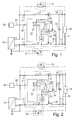
- the supply voltage terminals 11, 12 are over two current paths 14, 15 connected to two load terminals 16, 17 to which consumers are connected, in the embodiment, a consumer 18.
- To interrupt the current paths 14, 15 each have an electrical switch 19, 20, said switch 19, 20 through an electronic control device 21 are controllable.
- This electronic control device 21 can be a microcontroller or the control device 21 contains one or more microcontrollers.
- the electrical switches 19, 20 may be formed as a semiconductor switch or as a relay.
- An additional voltage source 22 forms, together with a current measuring resistor 23 and a further electrical switch 24, a series circuit which bridges the electrical switch 20, ie is connected between the negative supply voltage connection 12 and the negative consumer connection 17.
- the further electrical switch 24 is also controlled or switched by the electronic control device 21 and may also be formed as a semiconductor switch or relay.
- a measuring amplifier 26, which forms a current detection device 25 together with the current measuring resistor 23, has its output connected to a measuring input of the electronic control device 21, which has an A / D converter 27.
- this A / D converter 27 can also be designed as a separate structural unit.
- the electronic control device 21 can communicate with an external monitoring or control device 30 via a bus interface 28, to which a bus system 29 is connected, in particular emit error messages or status messages and / or receive external control signals, parameterization signals or programming signals.
- a Such communication can in principle also be wireless, for example via radio, Bluetooth or optical, magnetic, inductive or the like.
- the two consumer terminals 16, 17 are connected to each other via a capacitor 33, which serves as a buffer capacitor.
- the device described as an embodiment is used to detect possible faulty conclusions or cross-connections 31, 32, which bridge the switch 19 and / or the switch 20.
- These cross-connections 31, 32 are symbolized symbolically by a capacitor connected in parallel with a resistor.
- the electronic control device 21 For detection, the electronic control device 21 generates at regular or irregular time intervals very short test signals through which the two switches 19, 20 are opened during correspondingly short test intervals and the switch 24 is closed. As a result, the potential of the additional voltage source 22 is applied to the load terminal 17 via the current measuring resistor 23. As a result, the total potential of the load 18 changes by the amount of the voltage of the additional voltage source 22. If there is now an ohmic cross-circuit 32, which bridges the switch 20 or an ohmic cross-circuit 31, which bridges the switch 19, this leads to a static current the current measuring resistor 23, which is informed by the measuring amplifier 26 amplified via the A / D converter 27 of the control device 21.
- test interval or the test signal can be significantly less than 100 microseconds, which in particular with appropriate design of the capacitor 33 causes the consumer 18 no significant voltage dip occurs. Even without the capacitor 33, a corresponding design is possible.
- the current flow through the current measuring resistor 23 is measured once or several times during the test interval and appears as a digital signal via the A / D converter 27 in the control device 21. This meets due to the detected current value or the detected signal behavior, the decision whether a conclusion or Cross-circuit exists. From a maximum allowable limit then a faulty cross-circuit is detected, whereupon the controller 21, the two switches 19, 20 opens again until the error is corrected. As a result, the consumer 18 is switched off safely. In addition, a corresponding error signal can be stored and / or communicated to the external monitoring or control device 30 via the test system 29. If no faulty cross-circuiting is detected, the switches 19, 20 are closed again at the end of the test interval and the switch 24 is opened.
- the increase or decrease of the potential according to the invention during the test interval certainly leads to a current flow through the current measuring resistor 23, even if the undesired cross-circuit leads to an equally high potential.
- the potential increase occurs via a single path whose current flow is monitored during the short test interval.
- FIG. 2 illustrated second embodiment corresponds in construction and in the function largely to the first embodiment, so that the same or equivalent components or assemblies provided with the same reference numerals and are not described again.
- the only difference from the first embodiment is that the series connection of the additional voltage source 22 with the current measuring resistor 23 and the further switch 24 no longer bridges the switch 20, but is connected between the negative supply voltage terminal 11 and the positive load terminal 12. The mode of action remains the same.
- FIG. 3 illustrated third embodiment is functional against in the Figures 1 and 2 illustrated embodiments interchangeable and also has two supply voltage terminals 11, 12 for connection to a voltage source 13 and two consumer terminals 16, 17 for connection to a consumer 18.
- Some more ingredients of in FIG. 3 shown circuit arrangement 40 have a similar or identical structure as in the embodiments according to the Figures 1 and 2 However, for the sake of clarity, different reference numbers are provided.
- the circuit arrangement 40 comprises a control device 41, to which a current detection device 42 is connected.
- the current detection device 42 includes a, preferably measuring resistor 43, which is looped into the formed between the supply terminal 12 and the load terminal 17 current path 44.
- the measuring resistor 43 is associated with a measuring amplifier 45, which is designed to detect a voltage drop across the measuring resistor 43 and which is also the current detection device 42 associated. On the basis of the voltage drop determined by the measuring amplifier 45, the current can be deduced from the preferably low-impedance and thus low-loss measuring resistor 43 become.
- the measuring amplifier 45 is coupled to an analog-to-digital converter 46 arranged as an example in the control device 41, which performs a digitization of the analog signal of the determined voltage value provided by the measuring amplifier 45. The digitized measurement signal is further processed in the control device 41 in the manner described in more detail below.
- the control device 41 is connected via control lines 47 to 50 with switching means 51 to 54, which are looped by way of example in pairs in the current paths 44 and 55.
- the switching means 51 to 54 may be formed for example as a relay or as an electronic (semiconductor) switch and be switched by providing appropriate switching signals from the control device 41 via the control lines 47 to 50 between a release position and a blocking position.
- the switching means 51 and 52 are each designed to bridge a diode 56, 57 which is looped in the reverse direction in the respective current path 44, 55.
- switching means 51 and diode 56 or switching means 52 and diode 57 in each case form a voltage stage element 58, 59 which is independent for a switchable and at least essentially the operating state of the circuit arrangement 40, in particular with regard to the current flow in the circuit arrangement 40 Potential change in the respective current path 44, 55 is formed.
- the voltage step members 58, 59 are preferably driven counter-synchronously by the control device 41, so that in each case one of the two diodes 56, 57 is electrically bridged by the associated switching means 51 or 52.
- the switching means 53, 54 are, as in the embodiments according to the Figures 1 and 2 for disconnecting the load 18 from the supply voltage at the supply terminals 11, 12 provided.
- the diagnostic device which in particular comprises the control device 41, the current detection device 42 and the voltage stage elements 58, 59, serves for the detection of unwanted cross-circuits 61, 62 in the circuit arrangement 40.
- the load 18 is supplied via the circuit 40 with electrical energy, which is provided by the voltage source 13.
- the two voltage stage members 58, 59 are each driven counter-synchronously by the control device 41.
- the control device 41 it is provided that in each case one of the two switching means 51, 52 is in a closed position, in which the respectively associated diode 56, 57 is bridged, while the respective other switching means 51, 52 is in an open position.
- one of the two current paths 44, 55 a current flow through the diode 56, 57 instead, while in the other current path, a current flow at the diode 56, 57 over by the closed switching means 51, 52 takes place.
- the diodes are arranged in the current paths in each case in the reverse direction, so that instead of the voltage loss at the PN junction in each case the Zener voltage of the diode leads to the reduction of the electric potential.
- a difference is preferably formed between a first current value determined in the first operating state and a second current value determined in the second operating state, wherein the difference between the two current values is used as a measure for any cross-circuits present.
- the control device 41 can output an alarm signal if the determined difference of the two current values exceeds the limit value. This alarm signal can be forwarded, for example, to the control device 30, so that it receives via a bus system not shown in detail a communication with a machine control, not shown.
- a separation of the consumer 18 from the electrical supply to the load terminals 16, 17 may be provided by opening of the two switching means 53, 54 effected by the control device 41.
- the circuitry 40 may also be operated in a manner that verifies the function of the two switches 53 and 54.
- one of the two switches 53 or 54 is opened for a short time, in particular in the millisecond range, in order then to check, on the basis of the thereby adjusting current flow via the current detection device 42, whether a current flows despite the at least theoretically interrupted connection to the load 18. If so, it can at least be concluded that the opened switch 53 or 54 may malfunction and possibly not fully open.
- the device 10, 40 described in the exemplary embodiments is expediently designed as a compact electrical device which is connected between the supply voltage terminals 11, 12 and the load terminals 16, 17 or between the voltage source 13 and the at least one load 18.
- This device can be housed in a small compact case.
Landscapes
- Testing Of Short-Circuits, Discontinuities, Leakage, Or Incorrect Line Connections (AREA)
- Emergency Protection Circuit Devices (AREA)
Claims (15)
- Dispositif de surveillance d'un circuit électrique d'un circuit électrique récepteur contenant au moins un récepteur (18) électrique, sachant que deux bornes de tension d'alimentation (11, 12) sont raccordées, par l'intermédiaire de voies de courant (14, 15) présentant respectivement un commutateur (19,20), à deux bornes de récepteur (16, 17), auxquelles au moins un récepteur (18) est connecté ou peut être connecté, comprenant des moyens de commande (21) pour ouvrir les deux commutateurs (19, 20) dans les voies de courant (14, 15), caractérisé en ce qu'est prévue une source de tension (22) supplémentaire, dont le potentiel peut être appliqué au niveau d'une des bornes de récepteur (16, 17) au moyen d'un autre commutateur (24), sachant que les moyens de commande (21) sont prévus également afin de fermer l'autre commutateur (24) au cours de périodes de contrôle, et comprenant en outre des moyens de signal servant à produire des signaux d'anomalie en cas d'identification d'un courant supérieur à un flux de courant prédéfini ou pouvant être prédéfini circulant à travers l'autre commutateur (24).
- Dispositif selon la revendication 1, caractérisé en ce que les moyens de commande (21) et/ou les moyens de signal présentent au moins un microcontrôleur ou sont réalisés sous la forme d'un microcontrôleur de ce type.
- Dispositif selon la revendication 1 ou 2, caractérisé en ce que des moyens de détection du courant (25) sont disposés dans le circuit électrique de l'autre commutateur (24), lesdits moyens de détection du courant étant raccordés à un système d'analyse.
- Dispositif selon la revendication 3, caractérisé en ce que les moyens de détection de courant (25) présentent une résistance de mesure du courant (23) dans le circuit électrique de l'autre commutateur (24).
- Dispositif selon l'une quelconque des revendications précédentes, caractérisé en ce que le système d'analyse est raccordé aux moyens de commande (21) et/ou aux moyens de signal ou est intégré dans ces derniers, et/ou en ce que les deux bornes de récepteur (16, 17) sont raccordées l'une à l'autre par l'intermédiaire d'un condensateur (33), et/ou en ce que les périodes de contrôle présentent une courte durée ne portant pas préjudice ou, le cas échéant de manière négligeable, au fonctionnement du récepteur (18), et/ou en ce que les moyens de commande (21) et/ou les moyens de signal sont raccordés, par l'intermédiaire d'un système de bus (29) ou sans fil, à un système de surveillance ou de commande (30), et/ou en ce que les moyens de commande (21) comportent des moyens de mise hors service servant à ouvrir les deux commutateurs (19, 20) dans les voies de courant (14, 15) en cas d'identification d'une anomalie ou d'un dépassement de valeur limite, et/ou en ce que le dispositif est réalisé sous la forme d'un appareil électrique commuté entre la tension d'alimentation (13) et le récepteur (18) au moins au nombre de un.
- Ensemble formant circuit servant à alimenter un récepteur (18) en énergie électrique, comprenant au moins deux voies de courant (14, 15 ; 44, 55), qui s'étendent respectivement entre une borne d'alimentation (11, 12) associée pour injecter de l'énergie électrique dans l'ensemble formant circuit (10 ; 40) et une borne de récepteur (16, 17) pour la fourniture de l'énergie électrique à un récepteur (18), sachant qu'un système de diagnostic (21, 22, 25 ; 41, 42, 58, 59) est associé à des voies de courant (14, 15 ; 44, 55), lesquelles sont réalisées pour déterminer et traiter au moins une valeur caractéristique électrique afin de déterminer des dysfonctionnements de l'ensemble formant circuit (10 ; 40), caractérisé en ce que le système de diagnostic (21, 22, 25 ; 41, 42, 58, 59) comprend des moyens de réglage (19, 20, 22, 24 ; 58, 59), qui sont réalisés pour régler de manière variable des niveaux de potentiel au niveau des bornes de récepteur (16, 17) associées et pour fournir une différence de potentiel pouvant être prédéfinie entre les bornes de récepteur (16, 17).
- Ensemble formant circuit selon la revendication 6, caractérisé en ce que les moyens de réglage (19, 20, 22, 24, 33 ; 58, 59) sont réalisés pour un réglage alternatif de deux, en particulier précisément de deux, niveaux de potentiel différents au niveau de la borne de récepteur (16, 17) respectivement associée, et/ou en ce que les moyens de réglage (19, 20, 22, 24, 33 ; 58, 59) sont réalisés de telle manière qu'une différence de potentiel entre les bornes de récepteur (16, 17), qui dépend des niveaux de potentiel variables, qui est en particulier constante, est fournie au niveau des bornes de récepteur (16, 17) et/ou que le système de diagnostic (21, 22, 25 ; 41, 42, 58, 59) est réalisé de telle manière qu'une alimentation du récepteur (18) sans interruption et/ou constante en matière de tension est assurée avec une énergie électrique lors d'une période de contrôle, au cours de laquelle une vérification du circuit (10 ; 40) est effectuée, et/ou en ce que le système de diagnostic (21, 22, 25 ; 41, 42, 58, 59) comprend des moyens de mise hors service (19, 20 ; 53, 54) servant à ouvrir les deux voies de courant (14, 15 ; 44, 55) en cas d'identification d'une anomalie ou en cas de dépassement d'une valeur limite.
- Ensemble formant circuit selon l'une quelconque des revendications 6 ou 7, caractérisé en ce qu'un organe à étages de tension (22, 24 ; 58, 59) pouvant être commuté par le système de diagnostic (21, 22, 25 ; 41, 42, 58, 59) est bouclé, en tant que moyen de réglage, dans au moins une voie de courant (14, 15 ; 44, 55), laquelle s'étend entre une borne d'alimentation (11, 12) et une borne de récepteur (16, 17), ledit organe à étages de tension étant réalisé, pour un décalage de potentiel défini au niveau des bornes de récepteur (16, 17) lors d'un état de fonctionnement pouvant être prédéfini de l'ensemble formant circuit (10 ; 40).
- Ensemble formant circuit selon la revendication 8, caractérisé en ce que l'organe à étages de tension (22, 24 ; 58, 59) est réalisé sous la forme d'un circuit en parallèle d'une diode (56, 57) et d'un moyen de commutation (53, 54) pouvant être commandé par le système de diagnostic (41, 42, 58, 59), et/ou en ce que le système de diagnostic (41, 42, 58, 59) est réalisé pour la mise en oeuvre d'une période de contrôle pour une activation alternée des moyens de commutation (51, 52) dans les voies de courant (44, 55) équipées de l'organe à étages de tension (58, 59) afin de fournir, au niveau des bornes de récepteur (16, 17), des niveaux de potentiel pouvant être prédéfinis en présence d'une différence de potentiel constante entre les bornes de récepteur (16, 17).
- Ensemble formant circuit selon l'une quelconque des revendications 6 à 9, caractérisé en ce que le système de diagnostic (41, 42, 58, 59) est réalisé pour former une différence entre des valeurs caractéristiques électriques se réglant lors de l'activation alternée des moyens de commutation (51, 52) afin de permettre une évaluation d'un état de fonctionnement de l'ensemble formant circuit (40).
- Ensemble formant circuit selon la revendication 6, caractérisé en ce que respectivement un commutateur (19, 20) est disposé dans deux voies de courant (14, 15), en ce qu'est prévue une source de tension (22) supplémentaire, dont le potentiel peut être appliqué, au moyen d'un autre commutateur (24), au niveau d'une des bornes de récepteur (16, 17), en ce que le système de diagnostic (21, 22, 25) est réalisé pour ouvrir les deux commutateurs (19, 20) dans les voies de courant (14, 15) et pour fermer l'autre commutateur (24) au cours des périodes de contrôle, et en ce que le système de diagnostic (21, 22, 25) comprend des moyens de signal servant à produire des signaux d'anomalie en cas d'identification d'un courant supérieur à un flux de courant prédéfini ou pouvant être prédéfini, circulant à travers l'autre commutateur (24).
- Ensemble formant circuit selon la revendication 10, caractérisé en ce que des moyens de détection de courant (25) sont disposés dans le circuit électrique de l'autre commutateur (24), lesquels sont raccordés au système de diagnostic (21, 22, 25).
- Ensemble formant circuit selon la revendication 11, caractérisé en ce que les moyens de détection de courant (25) présentent une résistance de mesure de courant (23) dans le circuit électrique de l'autre commutateur (24), et/ou en ce que les deux bornes de récepteur (16, 17) sont raccordées entre elles par l'intermédiaire d'un condensateur (33).
- Ensemble formant circuit selon l'une quelconque des revendications 6 à 8, caractérisé en ce que le système de diagnostic (21, 22, 25 ; 41, 42, 58, 59) est raccordé, par l'intermédiaire d'un système de bus (29) ou sans fil, à un système externe de surveillance ou de commande (30).
- Procédé servant à faire fonctionner un ensemble formant circuit (10 ; 40) pour l'alimentation d'un récepteur (18) en énergie électrique, sachant que l'ensemble formant circuit (10 ; 40) comprend un système de diagnostic (21, 22, 25 ; 41, 42, 58, 59) servant à déterminer un état de fonctionnement de l'ensemble formant circuit (10 ; 40), lequel procédé comprend les étapes qui suivent consistant à : fournir une différence de potentiel électrique pouvant être prédéfinie au niveau de bornes de récepteur (16, 17) de l'ensemble formant circuit (10; 40), qui sont associées à un récepteur (18); déterminer une première valeur d'une valeur caractéristique électrique de l'ensemble formant circuit (10 ; 40) au moyen du système de diagnostic (21, 22, 25 ; 41, 42, 58, 59), caractérisé par les étapes qui suivent consistant à : décaler de manière synchrone les potentiels électriques au niveau des bornes de récepteur (16, 17) lors du maintien de la différence de potentiel de manière à assurer une alimentation constante et sans interruption du récepteur (18), déterminer une deuxième valeur de la valeur caractéristique électrique de l'ensemble formant circuit (10; 40) et calculer une différence entre la première valeur et la deuxième valeur en tant qu'indicateur d'un dysfonctionnement au moyen du système de diagnostic (21, 22, 25 ; 41, 42, 58, 59), comparer la différence calculée avec une valeur seuil pouvant être prédéfinie, fournir une notification d'anomalie en cas de dépassement de la valeur seuil pouvant être prédéfinie grâce à la différence obtenue par calcul.
Applications Claiming Priority (2)
| Application Number | Priority Date | Filing Date | Title |
|---|---|---|---|
| DE102010007784A DE102010007784A1 (de) | 2010-02-12 | 2010-02-12 | Vorrichtung zur elektrischen Stromkreisüberwachung |
| PCT/EP2011/000641 WO2011098282A1 (fr) | 2010-02-12 | 2011-02-11 | Dispositif de contrôle de circuit électrique, dispositif de commutation pour l'alimentation d'un récepteur et procédé permettant de faire fonctionner un dispositif de commutation |
Publications (2)
| Publication Number | Publication Date |
|---|---|
| EP2519960A1 EP2519960A1 (fr) | 2012-11-07 |
| EP2519960B1 true EP2519960B1 (fr) | 2014-12-10 |
Family
ID=43901717
Family Applications (1)
| Application Number | Title | Priority Date | Filing Date |
|---|---|---|---|
| EP11706743.9A Active EP2519960B1 (fr) | 2010-02-12 | 2011-02-11 | Dispositif de contrôle de circuit électrique, dispositif de commutation pour l'alimentation d'un récepteur et procédé de fonctionnement d'un dispositif de commutation |
Country Status (4)
| Country | Link |
|---|---|
| EP (1) | EP2519960B1 (fr) |
| CN (1) | CN102822930B (fr) |
| DE (1) | DE102010007784A1 (fr) |
| WO (1) | WO2011098282A1 (fr) |
Cited By (1)
| Publication number | Priority date | Publication date | Assignee | Title |
|---|---|---|---|---|
| DE102015003925A1 (de) | 2015-03-25 | 2016-09-29 | Festo Ag & Co. Kg | Sicherheitsgerichtete Lastschalteinrichtung und Verfahren zum Betreiben einer sicherheitsgerichteten Lastschalteinrichtung |
Families Citing this family (17)
| Publication number | Priority date | Publication date | Assignee | Title |
|---|---|---|---|---|
| DE102011054968A1 (de) * | 2011-10-31 | 2013-05-02 | Phoenix Contact Gmbh & Co. Kg | Sicherheitsgerichtetes Schaltgerät |
| EP2942851B1 (fr) | 2014-05-09 | 2016-07-13 | dSPACE digital signal processing and control engineering GmbH | Procédé de surveillance de la puissance d'un consommateur électrique |
| DE102014222878A1 (de) * | 2014-11-10 | 2016-05-12 | Leoni Bordnetz-Systeme Gmbh | Kraftfahrzeug-Versorgungsnetz |
| JP6390454B2 (ja) * | 2015-02-02 | 2018-09-19 | オムロン株式会社 | 継電ユニット、および継電回路の制御方法 |
| DE102015213156A1 (de) | 2015-07-14 | 2017-02-02 | Festo Ag & Co. Kg | Sicherheitsgerichtete Lastschalteinrichtung und Verfahren zum Betreiben einer sicherheitsgerichteten Lastschalteinrichtung |
| DE102016123269A1 (de) * | 2015-12-09 | 2017-06-14 | FEV Europe GmbH | Verfahren für eine elektrische Funktionsprüfung bei einem Fahrzeug |
| DE102016202834A1 (de) * | 2016-02-24 | 2017-08-24 | Robert Bosch Gmbh | Kommunikationsschnittstelle und Verfahren zum Betrieb einer Kommunikationsschnittstelle |
| DE102016106798A1 (de) * | 2016-04-13 | 2017-10-19 | R. Stahl Schaltgeräte GmbH | Modul zur Bereitstellung einer eigensicheren elektrischen Ausgangsleitung sowie explosionsgeschützte Leuchte |
| DE102016117169B4 (de) * | 2016-09-13 | 2020-07-02 | HELLA GmbH & Co. KGaA | System zur Energie- und/oder Datenübertragung |
| DE102016117821A1 (de) * | 2016-09-21 | 2018-03-22 | Pilz Gmbh & Co. Kg | Sicherheitsschaltung zum fehlersicheren Abschalten einer gefahrbringenden technischen Anlage |
| DE102016220948A1 (de) * | 2016-10-25 | 2018-04-26 | Robert Bosch Gmbh | Vorrichtung und Verfahren zur Diagnose der Erfassung eines mehrphasigen elektrischen Stroms |
| EP3562282B1 (fr) * | 2018-04-25 | 2021-07-07 | Siemens Aktiengesellschaft | Fond de panier |
| DE202018104044U1 (de) * | 2018-07-13 | 2019-10-15 | Wago Verwaltungsgesellschaft Mbh | Erdleiter-Überwachung |
| FR3093869B1 (fr) * | 2019-03-14 | 2021-04-09 | Legrand France | Appareil électrique pour alimenter ou non une charge en fonction de l’état passant ou bloqué d’un organe de commande |
| EP3754346A1 (fr) * | 2019-06-17 | 2020-12-23 | Lisa Dräxlmaier GmbH | Dispositif de détection, dispositif de commutation, système d'alimentation électrique, procédé de détection et procédé |
| DE102020208401A1 (de) * | 2020-07-03 | 2022-01-05 | Robert Bosch Gesellschaft mit beschränkter Haftung | Verfahren zur Absicherung insbesondere sicherheitsrelevanter Verbraucher in einem Kraftfahrzeug |
| DE102022114513A1 (de) * | 2022-06-09 | 2023-12-14 | Wieland Electric Gmbh | Sicheres Halbleiterrelais |
Family Cites Families (6)
| Publication number | Priority date | Publication date | Assignee | Title |
|---|---|---|---|---|
| US5539602A (en) * | 1994-10-19 | 1996-07-23 | Gte Airfone Incorporated | Ground fault interrupter |
| JP3789819B2 (ja) * | 2000-02-18 | 2006-06-28 | 三洋電機株式会社 | 電動車両のリレー溶着検出装置 |
| DE10127233C1 (de) | 2001-05-22 | 2002-11-28 | Pilz Gmbh & Co | Sicherheitsschaltmodul und Verfahren zur Prüfung des Abschaltvermögens eines Schaltelements in einem Sicherheitsschaltmodul |
| GB2381393B (en) * | 2001-10-26 | 2005-11-02 | Agco Gmbh & Co | Mobile high voltage network |
| MY146753A (en) * | 2006-04-26 | 2012-09-14 | Ind Teknologi Mikro Berhad | An earth leakage protection device with time alert feature |
| DE102008018244B3 (de) * | 2008-04-10 | 2009-11-19 | Continental Automotive Gmbh | Vorrichtung und Verfahren zum Erkennen eines Fehlers in einer Leistungsbrückenschaltung |
-
2010
- 2010-02-12 DE DE102010007784A patent/DE102010007784A1/de not_active Ceased
-
2011
- 2011-02-11 WO PCT/EP2011/000641 patent/WO2011098282A1/fr not_active Ceased
- 2011-02-11 CN CN201180018756.3A patent/CN102822930B/zh not_active Expired - Fee Related
- 2011-02-11 EP EP11706743.9A patent/EP2519960B1/fr active Active
Cited By (3)
| Publication number | Priority date | Publication date | Assignee | Title |
|---|---|---|---|---|
| DE102015003925A1 (de) | 2015-03-25 | 2016-09-29 | Festo Ag & Co. Kg | Sicherheitsgerichtete Lastschalteinrichtung und Verfahren zum Betreiben einer sicherheitsgerichteten Lastschalteinrichtung |
| US10263613B2 (en) | 2015-03-25 | 2019-04-16 | Festo Ag & Co. Kg | Safety-oriented load switching device and method for operating a safety-oriented load switching device |
| DE102015003925B4 (de) | 2015-03-25 | 2026-07-02 | Festo Se & Co. Kg | Sicherheitsgerichtete Lastschalteinrichtung und Verfahren zum Betreiben einer sicherheitsgerichteten Lastschalteinrichtung |
Also Published As
| Publication number | Publication date |
|---|---|
| DE102010007784A1 (de) | 2011-08-18 |
| WO2011098282A1 (fr) | 2011-08-18 |
| CN102822930A (zh) | 2012-12-12 |
| EP2519960A1 (fr) | 2012-11-07 |
| CN102822930B (zh) | 2015-04-08 |
Similar Documents
| Publication | Publication Date | Title |
|---|---|---|
| WO2011098282A1 (fr) | Dispositif de contrôle de circuit électrique, dispositif de commutation pour l'alimentation d'un récepteur et procédé permettant de faire fonctionner un dispositif de commutation | |
| DE102005055325C5 (de) | Sicherheitsschaltvorrichtung zum fehlersicheren Abschalten eines elektrischen Verbrauchers | |
| EP2208215B1 (fr) | Dispositif de commutation et procédé de contrôle d'un relais électromagnétique | |
| EP2980660B1 (fr) | Procédé et dispositif de surveillance et de commutation d'un circuit de charge | |
| DE4242792C2 (de) | Sicherheitsschalteranordnung | |
| DE102007002953A1 (de) | Schaltungsanordnung zur Ausgabe eines Schaltsignals | |
| EP3043220B1 (fr) | Dispositif et procede de surveillance fonctionnelle d'un moyen de commutation de securite | |
| EP2845211B1 (fr) | Système de surveillance d'un relais électromagnétique | |
| EP2546852B1 (fr) | Relais de sécurité bistable | |
| EP3745596B1 (fr) | Circuit d'entrée numérique permettant de recevoir des signaux d'entrée numérique d'au moins un émetteur de signaux | |
| DE102011120466B4 (de) | Elektronischer Schutzschalter und Verfahren zur Betätigung des Schutzschalters | |
| DE102010013322B4 (de) | Detektionsschaltung und Verfahren zum Betreiben einer Detektionsschaltung | |
| DE4436858C2 (de) | Überspannungsschutzeinrichtung | |
| AT501215B1 (de) | Überwachungseinrichtung | |
| WO2011085958A1 (fr) | Dispositif de contrôle de circuit électrique | |
| WO2023011768A1 (fr) | Unité de disjoncteur | |
| DE112011101763T5 (de) | Fehlerschutzschaltung für eine IEC-61158-Feldbus-Abzweigleitung und Verfahren zu deren Anwendung | |
| DE102012111070B4 (de) | Sicherheitsbezogene Vorrichtung zum sicheren Schalten einer elektrischen Last | |
| DE102008029680A1 (de) | Verfahren und elektronische Schaltung für eine elektronische Schaltungseinheit | |
| EP2876509B1 (fr) | Commande de sécurité | |
| DE102020124902A1 (de) | Ansteuerung einer Haltebremse | |
| DE102014206360A1 (de) | Verfahren zur Prüfung eines Selbsthaltemagneten eines Schalters und Prüfeinrichtung für den Selbsthaltemagneten | |
| BE1032100B1 (de) | Schutzschalter mit mechanischem Wechselschalter und Überwachungseinrichtung | |
| EP4481411A1 (fr) | Dispositif et procédé de surveillance d'une capacité de coupure | |
| DE102015003925A1 (de) | Sicherheitsgerichtete Lastschalteinrichtung und Verfahren zum Betreiben einer sicherheitsgerichteten Lastschalteinrichtung |
Legal Events
| Date | Code | Title | Description |
|---|---|---|---|
| PUAI | Public reference made under article 153(3) epc to a published international application that has entered the european phase |
Free format text: ORIGINAL CODE: 0009012 |
|
| 17P | Request for examination filed |
Effective date: 20120804 |
|
| AK | Designated contracting states |
Kind code of ref document: A1 Designated state(s): AL AT BE BG CH CY CZ DE DK EE ES FI FR GB GR HR HU IE IS IT LI LT LU LV MC MK MT NL NO PL PT RO RS SE SI SK SM TR |
|
| DAX | Request for extension of the european patent (deleted) | ||
| GRAP | Despatch of communication of intention to grant a patent |
Free format text: ORIGINAL CODE: EPIDOSNIGR1 |
|
| INTG | Intention to grant announced |
Effective date: 20140711 |
|
| GRAS | Grant fee paid |
Free format text: ORIGINAL CODE: EPIDOSNIGR3 |
|
| GRAA | (expected) grant |
Free format text: ORIGINAL CODE: 0009210 |
|
| AK | Designated contracting states |
Kind code of ref document: B1 Designated state(s): AL AT BE BG CH CY CZ DE DK EE ES FI FR GB GR HR HU IE IS IT LI LT LU LV MC MK MT NL NO PL PT RO RS SE SI SK SM TR |
|
| REG | Reference to a national code |
Ref country code: GB Ref legal event code: FG4D Free format text: NOT ENGLISH |
|
| REG | Reference to a national code |
Ref country code: CH Ref legal event code: EP |
|
| REG | Reference to a national code |
Ref country code: IE Ref legal event code: FG4D Free format text: LANGUAGE OF EP DOCUMENT: GERMAN |
|
| REG | Reference to a national code |
Ref country code: DE Ref legal event code: R096 Ref document number: 502011005223 Country of ref document: DE Effective date: 20150115 Ref country code: AT Ref legal event code: REF Ref document number: 701021 Country of ref document: AT Kind code of ref document: T Effective date: 20150115 |
|
| REG | Reference to a national code |
Ref country code: NL Ref legal event code: VDEP Effective date: 20141210 |
|
| REG | Reference to a national code |
Ref country code: NL Ref legal event code: VDEP Effective date: 20141210 |
|
| PG25 | Lapsed in a contracting state [announced via postgrant information from national office to epo] |
Ref country code: LT Free format text: LAPSE BECAUSE OF FAILURE TO SUBMIT A TRANSLATION OF THE DESCRIPTION OR TO PAY THE FEE WITHIN THE PRESCRIBED TIME-LIMIT Effective date: 20141210 Ref country code: FI Free format text: LAPSE BECAUSE OF FAILURE TO SUBMIT A TRANSLATION OF THE DESCRIPTION OR TO PAY THE FEE WITHIN THE PRESCRIBED TIME-LIMIT Effective date: 20141210 Ref country code: NO Free format text: LAPSE BECAUSE OF FAILURE TO SUBMIT A TRANSLATION OF THE DESCRIPTION OR TO PAY THE FEE WITHIN THE PRESCRIBED TIME-LIMIT Effective date: 20150310 Ref country code: ES Free format text: LAPSE BECAUSE OF FAILURE TO SUBMIT A TRANSLATION OF THE DESCRIPTION OR TO PAY THE FEE WITHIN THE PRESCRIBED TIME-LIMIT Effective date: 20141210 |
|
| REG | Reference to a national code |
Ref country code: LT Ref legal event code: MG4D |
|
| PG25 | Lapsed in a contracting state [announced via postgrant information from national office to epo] |
Ref country code: RS Free format text: LAPSE BECAUSE OF FAILURE TO SUBMIT A TRANSLATION OF THE DESCRIPTION OR TO PAY THE FEE WITHIN THE PRESCRIBED TIME-LIMIT Effective date: 20141210 Ref country code: LV Free format text: LAPSE BECAUSE OF FAILURE TO SUBMIT A TRANSLATION OF THE DESCRIPTION OR TO PAY THE FEE WITHIN THE PRESCRIBED TIME-LIMIT Effective date: 20141210 Ref country code: HR Free format text: LAPSE BECAUSE OF FAILURE TO SUBMIT A TRANSLATION OF THE DESCRIPTION OR TO PAY THE FEE WITHIN THE PRESCRIBED TIME-LIMIT Effective date: 20141210 Ref country code: SE Free format text: LAPSE BECAUSE OF FAILURE TO SUBMIT A TRANSLATION OF THE DESCRIPTION OR TO PAY THE FEE WITHIN THE PRESCRIBED TIME-LIMIT Effective date: 20141210 Ref country code: GR Free format text: LAPSE BECAUSE OF FAILURE TO SUBMIT A TRANSLATION OF THE DESCRIPTION OR TO PAY THE FEE WITHIN THE PRESCRIBED TIME-LIMIT Effective date: 20150311 |
|
| PG25 | Lapsed in a contracting state [announced via postgrant information from national office to epo] |
Ref country code: NL Free format text: LAPSE BECAUSE OF FAILURE TO SUBMIT A TRANSLATION OF THE DESCRIPTION OR TO PAY THE FEE WITHIN THE PRESCRIBED TIME-LIMIT Effective date: 20141210 |
|
| PG25 | Lapsed in a contracting state [announced via postgrant information from national office to epo] |
Ref country code: PT Free format text: LAPSE BECAUSE OF FAILURE TO SUBMIT A TRANSLATION OF THE DESCRIPTION OR TO PAY THE FEE WITHIN THE PRESCRIBED TIME-LIMIT Effective date: 20150410 Ref country code: RO Free format text: LAPSE BECAUSE OF FAILURE TO SUBMIT A TRANSLATION OF THE DESCRIPTION OR TO PAY THE FEE WITHIN THE PRESCRIBED TIME-LIMIT Effective date: 20141210 Ref country code: CZ Free format text: LAPSE BECAUSE OF FAILURE TO SUBMIT A TRANSLATION OF THE DESCRIPTION OR TO PAY THE FEE WITHIN THE PRESCRIBED TIME-LIMIT Effective date: 20141210 Ref country code: SK Free format text: LAPSE BECAUSE OF FAILURE TO SUBMIT A TRANSLATION OF THE DESCRIPTION OR TO PAY THE FEE WITHIN THE PRESCRIBED TIME-LIMIT Effective date: 20141210 Ref country code: EE Free format text: LAPSE BECAUSE OF FAILURE TO SUBMIT A TRANSLATION OF THE DESCRIPTION OR TO PAY THE FEE WITHIN THE PRESCRIBED TIME-LIMIT Effective date: 20141210 |
|
| PG25 | Lapsed in a contracting state [announced via postgrant information from national office to epo] |
Ref country code: IS Free format text: LAPSE BECAUSE OF FAILURE TO SUBMIT A TRANSLATION OF THE DESCRIPTION OR TO PAY THE FEE WITHIN THE PRESCRIBED TIME-LIMIT Effective date: 20150410 Ref country code: PL Free format text: LAPSE BECAUSE OF FAILURE TO SUBMIT A TRANSLATION OF THE DESCRIPTION OR TO PAY THE FEE WITHIN THE PRESCRIBED TIME-LIMIT Effective date: 20141210 |
|
| REG | Reference to a national code |
Ref country code: DE Ref legal event code: R097 Ref document number: 502011005223 Country of ref document: DE |
|
| PG25 | Lapsed in a contracting state [announced via postgrant information from national office to epo] |
Ref country code: LU Free format text: LAPSE BECAUSE OF FAILURE TO SUBMIT A TRANSLATION OF THE DESCRIPTION OR TO PAY THE FEE WITHIN THE PRESCRIBED TIME-LIMIT Effective date: 20150211 |
|
| REG | Reference to a national code |
Ref country code: CH Ref legal event code: PL |
|
| PLBE | No opposition filed within time limit |
Free format text: ORIGINAL CODE: 0009261 |
|
| STAA | Information on the status of an ep patent application or granted ep patent |
Free format text: STATUS: NO OPPOSITION FILED WITHIN TIME LIMIT |
|
| PG25 | Lapsed in a contracting state [announced via postgrant information from national office to epo] |
Ref country code: DK Free format text: LAPSE BECAUSE OF FAILURE TO SUBMIT A TRANSLATION OF THE DESCRIPTION OR TO PAY THE FEE WITHIN THE PRESCRIBED TIME-LIMIT Effective date: 20141210 Ref country code: MC Free format text: LAPSE BECAUSE OF FAILURE TO SUBMIT A TRANSLATION OF THE DESCRIPTION OR TO PAY THE FEE WITHIN THE PRESCRIBED TIME-LIMIT Effective date: 20141210 Ref country code: LI Free format text: LAPSE BECAUSE OF NON-PAYMENT OF DUE FEES Effective date: 20150228 Ref country code: CH Free format text: LAPSE BECAUSE OF NON-PAYMENT OF DUE FEES Effective date: 20150228 |
|
| 26N | No opposition filed |
Effective date: 20150911 |
|
| REG | Reference to a national code |
Ref country code: IE Ref legal event code: MM4A |
|
| PG25 | Lapsed in a contracting state [announced via postgrant information from national office to epo] |
Ref country code: IE Free format text: LAPSE BECAUSE OF NON-PAYMENT OF DUE FEES Effective date: 20150211 |
|
| REG | Reference to a national code |
Ref country code: FR Ref legal event code: PLFP Year of fee payment: 6 |
|
| PG25 | Lapsed in a contracting state [announced via postgrant information from national office to epo] |
Ref country code: SI Free format text: LAPSE BECAUSE OF FAILURE TO SUBMIT A TRANSLATION OF THE DESCRIPTION OR TO PAY THE FEE WITHIN THE PRESCRIBED TIME-LIMIT Effective date: 20141210 |
|
| PG25 | Lapsed in a contracting state [announced via postgrant information from national office to epo] |
Ref country code: MT Free format text: LAPSE BECAUSE OF FAILURE TO SUBMIT A TRANSLATION OF THE DESCRIPTION OR TO PAY THE FEE WITHIN THE PRESCRIBED TIME-LIMIT Effective date: 20141210 |
|
| REG | Reference to a national code |
Ref country code: FR Ref legal event code: PLFP Year of fee payment: 7 |
|
| REG | Reference to a national code |
Ref country code: AT Ref legal event code: MM01 Ref document number: 701021 Country of ref document: AT Kind code of ref document: T Effective date: 20160211 |
|
| PG25 | Lapsed in a contracting state [announced via postgrant information from national office to epo] |
Ref country code: HU Free format text: LAPSE BECAUSE OF FAILURE TO SUBMIT A TRANSLATION OF THE DESCRIPTION OR TO PAY THE FEE WITHIN THE PRESCRIBED TIME-LIMIT; INVALID AB INITIO Effective date: 20110211 Ref country code: BG Free format text: LAPSE BECAUSE OF FAILURE TO SUBMIT A TRANSLATION OF THE DESCRIPTION OR TO PAY THE FEE WITHIN THE PRESCRIBED TIME-LIMIT Effective date: 20141210 Ref country code: SM Free format text: LAPSE BECAUSE OF FAILURE TO SUBMIT A TRANSLATION OF THE DESCRIPTION OR TO PAY THE FEE WITHIN THE PRESCRIBED TIME-LIMIT Effective date: 20141210 Ref country code: AT Free format text: LAPSE BECAUSE OF NON-PAYMENT OF DUE FEES Effective date: 20160211 |
|
| PG25 | Lapsed in a contracting state [announced via postgrant information from national office to epo] |
Ref country code: CY Free format text: LAPSE BECAUSE OF FAILURE TO SUBMIT A TRANSLATION OF THE DESCRIPTION OR TO PAY THE FEE WITHIN THE PRESCRIBED TIME-LIMIT Effective date: 20141210 |
|
| PG25 | Lapsed in a contracting state [announced via postgrant information from national office to epo] |
Ref country code: BE Free format text: LAPSE BECAUSE OF NON-PAYMENT OF DUE FEES Effective date: 20150228 |
|
| PG25 | Lapsed in a contracting state [announced via postgrant information from national office to epo] |
Ref country code: TR Free format text: LAPSE BECAUSE OF FAILURE TO SUBMIT A TRANSLATION OF THE DESCRIPTION OR TO PAY THE FEE WITHIN THE PRESCRIBED TIME-LIMIT Effective date: 20141210 |
|
| REG | Reference to a national code |
Ref country code: FR Ref legal event code: PLFP Year of fee payment: 8 |
|
| PG25 | Lapsed in a contracting state [announced via postgrant information from national office to epo] |
Ref country code: MK Free format text: LAPSE BECAUSE OF FAILURE TO SUBMIT A TRANSLATION OF THE DESCRIPTION OR TO PAY THE FEE WITHIN THE PRESCRIBED TIME-LIMIT Effective date: 20141210 |
|
| PG25 | Lapsed in a contracting state [announced via postgrant information from national office to epo] |
Ref country code: AL Free format text: LAPSE BECAUSE OF FAILURE TO SUBMIT A TRANSLATION OF THE DESCRIPTION OR TO PAY THE FEE WITHIN THE PRESCRIBED TIME-LIMIT Effective date: 20141210 |
|
| REG | Reference to a national code |
Ref country code: DE Ref legal event code: R082 Ref document number: 502011005223 Country of ref document: DE Representative=s name: PATENTANWAELTE MAGENBAUER & KOLLEGEN PARTNERSC, DE Ref country code: DE Ref legal event code: R081 Ref document number: 502011005223 Country of ref document: DE Owner name: FESTO SE & CO. KG, DE Free format text: FORMER OWNER: FESTO AG & CO. KG, 73734 ESSLINGEN, DE Ref country code: DE Ref legal event code: R081 Ref document number: 502011005223 Country of ref document: DE Owner name: FESTO AG & CO. KG, DE Free format text: FORMER OWNER: FESTO AG & CO. KG, 73734 ESSLINGEN, DE |
|
| PGFP | Annual fee paid to national office [announced via postgrant information from national office to epo] |
Ref country code: IT Payment date: 20200221 Year of fee payment: 10 Ref country code: GB Payment date: 20200225 Year of fee payment: 10 |
|
| PGFP | Annual fee paid to national office [announced via postgrant information from national office to epo] |
Ref country code: FR Payment date: 20200220 Year of fee payment: 10 |
|
| GBPC | Gb: european patent ceased through non-payment of renewal fee |
Effective date: 20210211 |
|
| PG25 | Lapsed in a contracting state [announced via postgrant information from national office to epo] |
Ref country code: FR Free format text: LAPSE BECAUSE OF NON-PAYMENT OF DUE FEES Effective date: 20210228 Ref country code: GB Free format text: LAPSE BECAUSE OF NON-PAYMENT OF DUE FEES Effective date: 20210211 |
|
| PG25 | Lapsed in a contracting state [announced via postgrant information from national office to epo] |
Ref country code: IT Free format text: LAPSE BECAUSE OF NON-PAYMENT OF DUE FEES Effective date: 20210211 |
|
| P01 | Opt-out of the competence of the unified patent court (upc) registered |
Effective date: 20230623 |
|
| PGFP | Annual fee paid to national office [announced via postgrant information from national office to epo] |
Ref country code: DE Payment date: 20260129 Year of fee payment: 16 |