EP2530710A2 - Bonddraht, Anschlussstruktur, Halbleitervorrichtung und Herstellungsverfahren dafür - Google Patents
Bonddraht, Anschlussstruktur, Halbleitervorrichtung und Herstellungsverfahren dafür Download PDFInfo
- Publication number
- EP2530710A2 EP2530710A2 EP12169576A EP12169576A EP2530710A2 EP 2530710 A2 EP2530710 A2 EP 2530710A2 EP 12169576 A EP12169576 A EP 12169576A EP 12169576 A EP12169576 A EP 12169576A EP 2530710 A2 EP2530710 A2 EP 2530710A2
- Authority
- EP
- European Patent Office
- Prior art keywords
- bonding wire
- hardness
- aluminum alloy
- silicon
- aluminum
- Prior art date
- Legal status (The legal status is an assumption and is not a legal conclusion. Google has not performed a legal analysis and makes no representation as to the accuracy of the status listed.)
- Withdrawn
Links
Images


Classifications
-
- H—ELECTRICITY
- H10—SEMICONDUCTOR DEVICES; ELECTRIC SOLID-STATE DEVICES NOT OTHERWISE PROVIDED FOR
- H10W—GENERIC PACKAGES, INTERCONNECTIONS, CONNECTORS OR OTHER CONSTRUCTIONAL DETAILS OF DEVICES COVERED BY CLASS H10
- H10W72/00—Interconnections or connectors in packages
- H10W72/071—Connecting or disconnecting
- H10W72/075—Connecting or disconnecting of bond wires
-
- H—ELECTRICITY
- H10—SEMICONDUCTOR DEVICES; ELECTRIC SOLID-STATE DEVICES NOT OTHERWISE PROVIDED FOR
- H10W—GENERIC PACKAGES, INTERCONNECTIONS, CONNECTORS OR OTHER CONSTRUCTIONAL DETAILS OF DEVICES COVERED BY CLASS H10
- H10W72/00—Interconnections or connectors in packages
- H10W72/01—Manufacture or treatment
- H10W72/015—Manufacture or treatment of bond wires
- H10W72/01551—Changing the shapes of bond wires
-
- H—ELECTRICITY
- H10—SEMICONDUCTOR DEVICES; ELECTRIC SOLID-STATE DEVICES NOT OTHERWISE PROVIDED FOR
- H10W—GENERIC PACKAGES, INTERCONNECTIONS, CONNECTORS OR OTHER CONSTRUCTIONAL DETAILS OF DEVICES COVERED BY CLASS H10
- H10W72/00—Interconnections or connectors in packages
- H10W72/01—Manufacture or treatment
- H10W72/015—Manufacture or treatment of bond wires
- H10W72/01565—Thermally treating
-
- H—ELECTRICITY
- H10—SEMICONDUCTOR DEVICES; ELECTRIC SOLID-STATE DEVICES NOT OTHERWISE PROVIDED FOR
- H10W—GENERIC PACKAGES, INTERCONNECTIONS, CONNECTORS OR OTHER CONSTRUCTIONAL DETAILS OF DEVICES COVERED BY CLASS H10
- H10W72/00—Interconnections or connectors in packages
- H10W72/071—Connecting or disconnecting
- H10W72/075—Connecting or disconnecting of bond wires
- H10W72/07531—Techniques
- H10W72/07532—Compression bonding, e.g. thermocompression bonding
- H10W72/07533—Ultrasonic bonding, e.g. thermosonic bonding
-
- H—ELECTRICITY
- H10—SEMICONDUCTOR DEVICES; ELECTRIC SOLID-STATE DEVICES NOT OTHERWISE PROVIDED FOR
- H10W—GENERIC PACKAGES, INTERCONNECTIONS, CONNECTORS OR OTHER CONSTRUCTIONAL DETAILS OF DEVICES COVERED BY CLASS H10
- H10W72/00—Interconnections or connectors in packages
- H10W72/071—Connecting or disconnecting
- H10W72/075—Connecting or disconnecting of bond wires
- H10W72/07541—Controlling the environment, e.g. atmosphere composition or temperature
-
- H—ELECTRICITY
- H10—SEMICONDUCTOR DEVICES; ELECTRIC SOLID-STATE DEVICES NOT OTHERWISE PROVIDED FOR
- H10W—GENERIC PACKAGES, INTERCONNECTIONS, CONNECTORS OR OTHER CONSTRUCTIONAL DETAILS OF DEVICES COVERED BY CLASS H10
- H10W72/00—Interconnections or connectors in packages
- H10W72/071—Connecting or disconnecting
- H10W72/075—Connecting or disconnecting of bond wires
- H10W72/07551—Connecting or disconnecting of bond wires characterised by changes in properties of the bond wires during the connecting
- H10W72/07555—Connecting or disconnecting of bond wires characterised by changes in properties of the bond wires during the connecting changes in materials
-
- H—ELECTRICITY
- H10—SEMICONDUCTOR DEVICES; ELECTRIC SOLID-STATE DEVICES NOT OTHERWISE PROVIDED FOR
- H10W—GENERIC PACKAGES, INTERCONNECTIONS, CONNECTORS OR OTHER CONSTRUCTIONAL DETAILS OF DEVICES COVERED BY CLASS H10
- H10W72/00—Interconnections or connectors in packages
- H10W72/50—Bond wires
- H10W72/531—Shapes of wire connectors
- H10W72/533—Cross-sectional shape
-
- H—ELECTRICITY
- H10—SEMICONDUCTOR DEVICES; ELECTRIC SOLID-STATE DEVICES NOT OTHERWISE PROVIDED FOR
- H10W—GENERIC PACKAGES, INTERCONNECTIONS, CONNECTORS OR OTHER CONSTRUCTIONAL DETAILS OF DEVICES COVERED BY CLASS H10
- H10W72/00—Interconnections or connectors in packages
- H10W72/50—Bond wires
- H10W72/531—Shapes of wire connectors
- H10W72/5363—Shapes of wire connectors the connected ends being wedge-shaped
-
- H—ELECTRICITY
- H10—SEMICONDUCTOR DEVICES; ELECTRIC SOLID-STATE DEVICES NOT OTHERWISE PROVIDED FOR
- H10W—GENERIC PACKAGES, INTERCONNECTIONS, CONNECTORS OR OTHER CONSTRUCTIONAL DETAILS OF DEVICES COVERED BY CLASS H10
- H10W72/00—Interconnections or connectors in packages
- H10W72/50—Bond wires
- H10W72/551—Materials of bond wires
- H10W72/552—Materials of bond wires comprising metals or metalloids, e.g. silver
- H10W72/5524—Materials of bond wires comprising metals or metalloids, e.g. silver comprising aluminium [Al]
-
- H—ELECTRICITY
- H10—SEMICONDUCTOR DEVICES; ELECTRIC SOLID-STATE DEVICES NOT OTHERWISE PROVIDED FOR
- H10W—GENERIC PACKAGES, INTERCONNECTIONS, CONNECTORS OR OTHER CONSTRUCTIONAL DETAILS OF DEVICES COVERED BY CLASS H10
- H10W72/00—Interconnections or connectors in packages
- H10W72/50—Bond wires
- H10W72/59—Bond pads specially adapted therefor
-
- H—ELECTRICITY
- H10—SEMICONDUCTOR DEVICES; ELECTRIC SOLID-STATE DEVICES NOT OTHERWISE PROVIDED FOR
- H10W—GENERIC PACKAGES, INTERCONNECTIONS, CONNECTORS OR OTHER CONSTRUCTIONAL DETAILS OF DEVICES COVERED BY CLASS H10
- H10W72/00—Interconnections or connectors in packages
- H10W72/90—Bond pads, in general
- H10W72/951—Materials of bond pads
- H10W72/952—Materials of bond pads comprising metals or metalloids, e.g. PbSn, Ag or Cu
-
- H—ELECTRICITY
- H10—SEMICONDUCTOR DEVICES; ELECTRIC SOLID-STATE DEVICES NOT OTHERWISE PROVIDED FOR
- H10W—GENERIC PACKAGES, INTERCONNECTIONS, CONNECTORS OR OTHER CONSTRUCTIONAL DETAILS OF DEVICES COVERED BY CLASS H10
- H10W90/00—Package configurations
-
- H—ELECTRICITY
- H10—SEMICONDUCTOR DEVICES; ELECTRIC SOLID-STATE DEVICES NOT OTHERWISE PROVIDED FOR
- H10W—GENERIC PACKAGES, INTERCONNECTIONS, CONNECTORS OR OTHER CONSTRUCTIONAL DETAILS OF DEVICES COVERED BY CLASS H10
- H10W90/00—Package configurations
- H10W90/701—Package configurations characterised by the relative positions of pads or connectors relative to package parts
- H10W90/751—Package configurations characterised by the relative positions of pads or connectors relative to package parts of bond wires
- H10W90/753—Package configurations characterised by the relative positions of pads or connectors relative to package parts of bond wires between laterally-adjacent chips
-
- H—ELECTRICITY
- H10—SEMICONDUCTOR DEVICES; ELECTRIC SOLID-STATE DEVICES NOT OTHERWISE PROVIDED FOR
- H10W—GENERIC PACKAGES, INTERCONNECTIONS, CONNECTORS OR OTHER CONSTRUCTIONAL DETAILS OF DEVICES COVERED BY CLASS H10
- H10W90/00—Package configurations
- H10W90/701—Package configurations characterised by the relative positions of pads or connectors relative to package parts
- H10W90/751—Package configurations characterised by the relative positions of pads or connectors relative to package parts of bond wires
- H10W90/754—Package configurations characterised by the relative positions of pads or connectors relative to package parts of bond wires between a chip and a stacked insulating package substrate, interposer or RDL
Definitions
- the present invention relates to a bonding wire and a connection structure suitable for a power semiconductor, a semiconductor device provided with these, and a manufacturing method thereof.
- a Si device which is a kind of a semiconductor is used as a discrete element such as a diode, a transistor and a thyristor, and as an integrated circuit such as a microcomputer, a memory and a communication device.
- a Si device works for computation and memorization.
- a Si device called a power semiconductor and is used in power control. Thanks to a power semiconductor, rectification, frequency conversion, boosting and back-boosting and the like are possible.
- a power semiconductor is used in various uses, such as driving of a motor and charging of a battery.
- power MOSFET metal-oxide-semiconductor field-effect transistor
- IGBT insulated gate bipolar transistor
- a power bipolar transistor a thyristor and the like.
- an IGBT is widely used in the market because of a large device capacity and a large range of adaptable operating frequency, excellent cost performance and the like.
- an IGBT is industrially used as a module structure in which a plurality of silicon chips are connected in parallel. Although the amount of a current flowing in one silicon chip is on the order of 100 A maximum, it is possible to handle a large current by adopting a module structure.
- Such an IGBT is used in a power generator using wind force, sunlight and the like, an industrial robot, an inverter in an automobile or an electric train, and the like.
- HV hybrid vehicles
- electric vehicles due to an increase in hybrid vehicles (HV) and electric vehicles, the frequency of uses in automobiles has increased.
- Breakages of an IGBT due to heat generation are divided into those caused by the deterioration of solder connections between a copper plate functioning as a heat sink and a ceramic substrate on which silicon chips are placed and those caused by the deterioration of the silicon chips and bonding wire connections.
- the deterioration of the bonding wire connections is due to thermal stresses generated by the repetition of the heating and cooling cycle during operation of a power module, and this is the result of the propagation of cracks, which occur due to a difference in the coefficient of linear expansion between the bonding wire and the silicon chips, in the vicinity of an interface.
- the present invention was made in order to solve the above-described problem, and the object of the invention is to provide a bonding wire which prevents the generation and propagation of cracks in a connection to a connected member, a connection structure of the bonding wire, a semiconductor device provided with these and a manufacturing method of the semiconductor device.
- the present invention provides a bonding wire characterized in consisting of an aluminum alloy which contains at least magnesium and silicon and in that a total of contents of the magnesium and the silicon is not less than 0.03 wt% but not more than 1.0 wt%.
- the generation of cracks is prevented by the solid-solution hardening by magnesium and silicon. Furthermore, by subjecting a bonding wire to aging treatment, a compound consisting of magnesium and silicon, for example, Mg 2 Si (called magnesium silicide) precipitates within the bonding wire, and the precipitation hardening by this compound prevents the propagation of cracks even when the cracks are generated in a connection to a connected member.
- a compound consisting of magnesium and silicon for example, Mg 2 Si (called magnesium silicide) precipitates within the bonding wire, and the precipitation hardening by this compound prevents the propagation of cracks even when the cracks are generated in a connection to a connected member.
- the present invention provides also the bonding wire in (1) above characterized in having a diameter of not less than 10 ⁇ m but not more than 500 ⁇ m.
- the present invention provides also the bonding wire in (1) or (2) above characterized in that with the amount of increase in maximum hardness from an initial hardness to a maximum hardness due to aging treatment as a standard, aging treatment is performed until an increase in hardness of not less than 40% of the amount of increase in the maximum hardness is obtained.
- the hardness of the bonding wire has not reached a maximum hardness, in connecting the bonding wire to a connected member, it is possible to prevent the connected member from being damaged due to the hardness of the bonding wire.
- the age-hardening of the bonding wire proceeds more due to the heat generation during use. As a result of this, a longer operating life of this connection is achieved.
- the present invention provides also the bond ing wire in any of (1) to (3) above characterized in that the hardness becomes not more than 45 Hmv.
- the present invention provides also the bonding wire in (4) above characterized in that the hardness becomes not more than 35 Hmv.
- the present invention provides also the bonding wire in any of (1) to (5) above characterized in that the aluminum alloy contains not less than 0.1 wt% but not more than 1.0 wt% of copper.
- hardness is improved further because of the precipitation of Al 2 Cu particles and Al 2 CuMg particles.
- the present invention provides also the bonding wire in any of (1) to (6) above characterized in that the aluminum alloy contains not less than 0.001 wt% but not more than 0.01 wt% of nickel.
- connection structure characterized in being a connection structure between the bonding wire in any of (1) to (7) above and a connected member to which the bonding wire is connected and which consists of an aluminum material, and in that a compound containing magnesium and silicon precipitates in a matrix layer constituting the bonding wire, in a fine grain layer of the aluminum alloy formed between the matrix layer and the connected member, and at an interface between the matrix layer and the fine grain layer.
- the generation of cracks is prevented by the solid-solution hardening and precipitation hardening by the magnesium and silicon contained in the bonding wire consisting of an aluminum alloy. Furthermore, thanks to the precipitation hardening by a compound, in the case where a crack is generated in a connection to a connected member, the propagation of the crack is prevented.
- the present invention also provides the connection structure in (8) above characterized in that the compound contains aluminum.
- the present invention also provides the connection structure in (8) or (9) above characterized in that the amount of precipitation of the compound is not less than 0.5% in terms of the area ratio of a section in the direction of the interface.
- the present invention also provides a semiconductor device characterized in having the connection structure in any of (8) to (10) above.
- the present invention also provides a method of manufacturing the semiconductor device according to (11) above characterized in that after the bonding wire is connected to the connected member, the bonding wire is subjected to aging treatment.
- connection structure in any of (8) to (10) above, the semiconductor device in (11) above, and the method of manufacturing the semiconductor device in (12) above it is possible to prevent the generation and propagation of cracks in a connection to a connected member.
- Figure 1 is an appearance perspective view of a semiconductor device of the present invention
- Figure 2 is a sectional view of the main part of the semiconductor device shown in Figure 1 ;
- Figure 3 (A) is a sectional view of a connection structure provided in the semiconductor device shown in Figure 1 ;
- Figures 3 (B) and 3 (C) are pictures obtained by photographing sections at the interface between a matrix layer and a fine grain layer shown in Figure 3 (A) ;
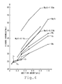
- Figure 4 is a graph showing the hardness of aluminum alloys, the addition amount on the abscissa and the hardness of the aluminum alloys on the ordinate;
- Figures 5 (A) and 5 (B) are each graphs showing the transition of hardness by aging treatment, with treatment time on the abscissa and hardness on the ordinate;
- Figures 6 (A) and 6 (B) are graphs showing the shear strength in the connection structure shown in Figures 3 (A) to 3 (C) , with the heating and cooling cycle number on the abscissa and shearing strength on the ordinate;
- Figures 7 (A) and 7 (B) are graphs showing the deterioration rate of shearing strength in the connection structure shown in Figures 3 (A) to 3 (C) , with the heating and cooling cycle number on the abscissa and the deterioration rate of shearing strength on the ordinate;
- Figure 8 is a graph showing the deterioration rate of shearing strength in the connection structure shown in Figures 3 (A) to 3 (C) , with the addition amount of magnesium silicide on the abscissa and the deterioration rate of shearing strength on the ordinate;
- Figure 9 is a graph showing the transition of tensile strength by aging treatment, with treatment time on the abscissa and tensile strength on the ordinate;
- Figures 10 (A) and 10 (B) are each graphs showing the hardness of an aluminum alloy, with the addition amount on the abscissa and the hardness of the aluminum alloy on the ordinate.
- Figure 1 is an appearance perspective view of the semiconductor device 10.
- Figure 2 is a sectional view of the main part of the semiconductor device 10.
- Figure 3 (A) is a sectional view of a connection structure 15.
- Figure 3 (B) is a picture obtained by photographing a section at the interface between a matrix layer 17a and a fine grain layer 17b, showing the portion in which a compound 18 is formed as a rod-like precipitate.
- Figure 3 (C) is a picture obtained by photographing a section at the interface between the matrix layer 17a and the fine grain layer 17b, showing the portion in which the compound 18 is formed as a granular precipitate.
- the semiconductor device 10 shown in Figures 1 and 2 is an IGBT module, which is a kind of power semiconductor. This semiconductor device 10 is mounted on a hybrid car and the like and is used in the control of electric power.
- the semiconductor device 10 is provided with a copper plate (a Cu plate) 11 which functions as a heat sink, a ceramics substrate 19 arranged on this copper plate 11, an enclosure 12 made of resin and the like.
- a copper plate (a Cu plate) 11 which functions as a heat sink
- a ceramics substrate 19 arranged on this copper plate 11, an enclosure 12 made of resin and the like.
- a plurality of circuit layers 13, a pluralityofsiliconchips (Sichips) 16 a plurality of bonding wires 17 which are arranged between these plurality of silicon chips 16 or between the silicon chip 16 and the circuit layer 13.
- the circuit layers 13 and the silicon chips 16 function as connectedmembers to which the bonding wires 17 are connected.
- an aluminum electrode pad 16a is deposited on the silicon chip 16.
- the bonding wire 17 is joined to the aluminum electrode pad 16a deposited on the silicon chip 16.
- the bonding wire 17 is made of an aluminum (Al) alloy.
- the aluminum alloy contains at least magnesium (Mg) and silicon and it is preferred that a total of contents of the magnesium and the silicon be not less than 0.03 wt% but not more than 1.0 wt%. It is more preferred that the total be not less than 0.1 wt% but not more than 0.9 wt%. It is still more preferred that the total be not less than 0.2 wt% but not more than 0.7 wt%.
- the total content of magnesium and silicon be not less than 0.03 wt% is that if the total content of magnesium and silicon is less than this value, in the first place, it is impossible to obtain the hardness of the aluminum alloy.
- Thebondingwire 17 is for use in power semiconductors and has a prescribed diameter. It is preferred that the diameter of the bonding wire 17 be not less than 10 ⁇ m but not more than 500 ⁇ m. Preferably, this diameter is not less than 100 ⁇ m but not more than 500 ⁇ m.
- the bonding wire 17 is of a type for use in bonding at ordinary temperature of not more than 60°C, it is preferred that the bonding wire 17 have hardness of not more than 35 Hmv (Vickers hardness) before aging treatment or during aging treatment, and the bonding wire 17 is hardened by aging treatment before or after bonding. Also, the bonding wire 17 is of a type for use in bonding at high temperatures of not less than 160°C but not more than 220°C, it is preferred that the bonding wire 17 have hardness of not more than 45 Hmv at ordinary temperature before aging treatment or during aging treatment and hardness of not more than 35 Hmv (Vickers hardness) at high temperatures, and the bonding wire 17 is hardened by aging treatment before or after bonding.
- Reference numeral 15 in Figure 3(A) denotes a connection structure between the silicon chip 16 and the bonding wire 17 .
- this connection structure 15 the bonding wire 17 is joined to the silicon chip 16.
- An ultrasonic joining technology which involves applying ultrasonic oscillations is used in joining the bonding wire 17.
- aging treatment whose treatment temperature is ordinary temperature to 300°C is performed.
- the aging treatment requires a treatment time which is such that, with the amount of increase in maximum hardness from an initial hardness to a maximum hardness due to the aging treatment as a standard, the aging treatment is performed until hardness of not less than 40% of the amount of increase in the maximum hardness is obtained. It is preferred that the aging treatment be performed for a treatment time until hardness of not less than 40% but not more than 70% of the amount of increase in the maximum hardness is obtained.
- the silicon chip 16 is such that on the surface thereof there is formed an aluminum-silicon film 16a made of an aluminum material which functions as an aluminum electrode pad.
- the bonding wire 17 has a matrix layer 17a and a fine grain layer 17b of aluminum alloy which is formed between this matrix layer 17a and the silicon film 16a.
- This fine grain layer 17b is formed by the recrystallization of a strained area occurring during ultrasonic joining.
- a compound 18 containing magnesium and silicon is formed in the matrix layer 17a, in the fine grain layer 17b, and at an interface between the matrix layer 17a and the fine grain layer 17b.
- the compound 18 containing magnesium and silicon precipitates due to aging treatment.
- the compound 18 precipitates in amounts of not less than 0.5% in terms of the area ratio in a section in the direction of the interface between the fine grain layer 17b and the aluminum-silicon film 16a (in the horizontal direction in Figure 3(A) ), even in the case where a crack is generated in the connection of the bonding wire 17 to the silicon chip 16, the propagation of this crack is prevented.
- Figures 3 (B) and 3 (C) show the case where a bonding wire 17 made of an aluminum alloy containing 0.5 wt% of magnesium silicide (Mg 2 Si) was subjected to solution treatment at 400°C for 1 hour and then to aging hardening treatment at 200°C for 4 hours.
- Mg 2 Si magnesium silicide
- various kinds of aluminum alloys were used as samples.
- the various kinds of aluminum alloys were obtained by adding, to aluminum, each of copper, magnesium, magnesium silicide, iron (Fe), manganese (Mn), chromium (Cr) and zirconium (Zr) or a mixture obtained by adding 0.01 wt% of nickel (Ni), 0.1 wt% of copper or 1 wt% of copper to magnesium silicide.
- the various kinds of aluminum alloys used were used immediately after casting and were not subjected to aging treatment.
- the investigation was conducted in each of the cases where the addition amount of copper is 0.2 wt%, 0.3 wt%, 0.5 wt% and 1.0 wt%.
- the investigation was conducted in each of the cases where the addition amount of magnesium silicide is 0.2 wt%, 0.3 wt%, 0.5 wt%, 0.8 wt% and 1.0 wt%.
- the investigation was conducted in each of the cases where the magnesium or manganese contents are 0.3 wt%, 0.5 wt% and 1.0 wt%.
- the aluminum alloys containing magnesium silicide have higher hardness than the aluminum alloys containing copper and were regarded as good in the evaluation.
- the aluminum alloy containing magnesium silicide has hardness on the order of 1.25 times the hardness of the aluminum alloys containing copper and were regarded as good in the evaluation.
- magnesium silicide At all of the addition amounts of magnesium silicide, the aluminum alloys containing magnesium silicide to which 0.01 wt% of nickel is added, magnesium silicide to which 0.1 wt% of copper is added, and magnesium silicide to which 1 wt% of copper is added, have higher hardness than the aluminum alloys containing copper and were regarded as good in the evaluation.
- the aluminum alloys containing magnesium have hardness equal to the hardness of the aluminum alloys containing copper and were regarded as good in the evaluation.
- the aluminum alloys containing iron, manganese, chromium or zirconium have lower hardness than the aluminum alloys containing copper and were regarded as bad in the evaluation.
- the hardness of the various kinds of aluminum alloys showed larger values than the pure aluminum alloys.
- the hardness of the aluminum alloy containing 0.5 wt% of copper and of the aluminum alloy containing 0.3 wt% of magnesium was substantially constant regardless of the transition of time.
- the hardness of the aluminum alloy containing 0.3 wt% of magnesium silicide continued to increase until 9000 minutes and decreased gradually from 9000 minutes. That is, in the aluminum alloy containing 0.3 wt% of magnesium silicide, aging hardening was observed in the period until 9000 minutes.
- Figures 6 (A), 6 (B) and Figures 7 (A), 7 (B) are graphs showing the shear strength in the connection structure 15, with the heating and cooling cycle number [times] on the abscissa and shearing strength [N] on the ordinate.
- Shearing strength refers to a maximum shearing force under which the material constituting the connection structure 15 can withstand without a break.
- Figures 7 (A) and 7 (B) are graphs showing the deterioration rate of shearing strength in the connection structure 15, with the heating and cooling cycle number [times] on the abscissa and the deterioration rate of shearing strength [%] on the ordinate.
- the deterioration rate of shearing strength refers to a value which indicates by percentage the degree of deterioration based on the case where the heating and cooling cycle number is 0 times.
- each plot shown in the graphs is an average value obtained by conducting the experiment 16 times. The sharing strength of various kinds of aluminum alloys was investigated at room temperature.
- the shearing strength decreased with increasing heating and cooling cycle number, that is, the deterioration rate of shearing strength increased.
- Figure 8 is a graph showing the deterioration rate of shearing strength in the connection structure 15, with the addition amount [wt%] of magnesium silicide on the abscissa and the deterioration rate of shearing strength [%] on the ordinate.
- the data obtained in Experiment 3 is used as the data necessary for Experiment 4. That is, repetitions of heat generation and heat dissipation due to the use of the semiconductor device 10 were created in a simulated manner.
- One heating and cooling cycle has a heating step for heating from 70°C to 120°C in 100 seconds and a cooling step for cooling from 120°C to 70°C in 70 seconds immediately thereafter. Each heating and cooling cycle was repeated 10000 times without an interval.
- the sharing strength of various kinds of aluminum alloys was investigated at room temperature.
- the aluminum alloys containing magnesium silicide have lower deterioration rates than the aluminum alloy containing copper and were regarded as good in the evaluation.
- Figure 9 is a graph showing the transition of tensile strength by aging treatment, with treatment time [hours] on the abscissa and tensile strength [MPa] on the ordinate. Incidentally, the investigation was conducted at a strain rate of 2 %/minute at room temperature. A bonding wire having a diameter of 0.3 mm and a length of 50 mm was used as the test piece.
- the tensile strength of the aluminum alloy containing magnesium silicide showed large values regardless of the aging time compared to the aluminum alloy containing copper or nickel. Furthermore, the tensile strength of the aluminum alloy containing magnesium silicide increased with increasing aging time.
- Figures 10 (A) and 10 (B) are each graphs showing the hardness of an aluminum alloy, with the addition amount [wt%] on the abscissa and the hardness [Hmv] of the aluminum alloy on the ordinate.
- the hardness of the aluminum alloys was investigated by a Vickers hardness test at room temperature.
- the hardness after solution treatment (hardness before aging treatment, initial hardness by aging treatment) and the maximum hardness by aging treatment
- the investigation was conducted in each of the cases where the addition amount of magnesium silicide is 0.2 wt%, 0.3 wt%, 0.5 wt% and 1.0 wt%.
- the addition amount is 0.01 wt%, 0.03 wt%, 0.1 wt%, 0.2 wt%, 0.3 wt%, 0.5 wt% and 1.0 wt%.
- an amount of change in hardness until a maximum hardness by aging treatment equals "maximum hardness by aging treatment” minus "hardness after solution treatment”.
- the generation of cracks in the bonding wire 17 is prevented by the solid-solution hardening by the magnesium and silicon contained in the bonding wire 17. Furthermore, even in the case where a crack is generated in a connection of the bonding wire 17 to the silicon chip 16, the propagation of the crack is prevented by the precipitation hardening of the compound 18 which precipitates at an interface between the fine grain layer 17b and the aluminum-silicon film 16a.
- the bonding wire 17 has not reached a maximum hardness, in connecting the bonding wire 17 to the silicon chip 16, the silicon chip 16 is prevented from being damaged due to the hardness of the bonding wire 17.
- the aging hardening of the bonding wire 17 due to heat generation proceeds further. As a result of this, an improvement in the operation life of the connection structure 15 is further achieved.
- the present invention is not limited to the above-described embodiment, and various kinds of variations are possible so long as such variations do not depart from the gist and technical philosophy of the invention.
- the bonding wire 17 may contain not less than 0.001 wt% but not more than 0.01 wt% of nickel or not less than 0.1 wt% but not more than 1.0 wt% of copper.
- nickel When nickel is added, humidity resistance is improved.
- copper When copper is added, hardness is further improved.
- aging treatment is performed for treatment time until hardness of not less than 40% of the amount of increase in the maximum hardness is obtained, a wire before joining may sometimes be subjected to aging hardening until a maximum hardness. Also, there is the case where aging treatment is not performed before joining and aging hardening proceeds at a working temperature after joining.
- a semiconductor device 10 is provided with a connection structure 15 between a bonding wire 17 consisting of an aluminum alloy which contains at least magnesium and silicon and in which a total of contents of the magnesium and the silicon is not less than 0.03 wt% but not more than 1.0 wt% and a silicon chip 16 to which this bonding wire 17 is connected.
- An aluminum-silicon film 16a is formed on the surface of the silicon chip 16.
- This connection structure 15 has a compound 18 containingmagnesium and silicon in a matrix layer 17a constituting the bonding wire 17, in a fine grain layer 17b of the aluminum alloy formed between the matrix layer 17a and the aluminum-silicon film 16a, and at an interface between the matrix layer 17a and the fine grain layer 17b.
Landscapes
- Wire Bonding (AREA)
Applications Claiming Priority (1)
| Application Number | Priority Date | Filing Date | Title |
|---|---|---|---|
| JP2011125556 | 2011-06-03 |
Publications (2)
| Publication Number | Publication Date |
|---|---|
| EP2530710A2 true EP2530710A2 (de) | 2012-12-05 |
| EP2530710A3 EP2530710A3 (de) | 2013-10-16 |
Family
ID=46147356
Family Applications (1)
| Application Number | Title | Priority Date | Filing Date |
|---|---|---|---|
| EP12169576.1A Withdrawn EP2530710A3 (de) | 2011-06-03 | 2012-05-25 | Bonddraht, Anschlussstruktur, Halbleitervorrichtung und Herstellungsverfahren dafür |
Country Status (2)
| Country | Link |
|---|---|
| EP (1) | EP2530710A3 (de) |
| JP (1) | JP2013012728A (de) |
Cited By (1)
| Publication number | Priority date | Publication date | Assignee | Title |
|---|---|---|---|---|
| EP2738805A1 (de) * | 2012-11-30 | 2014-06-04 | Nippon Piston Ring Co., Ltd. | Aluminiumbonddraht, Anschlussstruktur, Halbleitervorrichtung und Herstellungsverfahren dafür |
Citations (1)
| Publication number | Priority date | Publication date | Assignee | Title |
|---|---|---|---|---|
| JP2008311383A (ja) | 2007-06-14 | 2008-12-25 | Ibaraki Univ | ボンディングワイヤ、それを使用したボンディング方法及び半導体装置並びに接続部構造 |
Family Cites Families (7)
| Publication number | Priority date | Publication date | Assignee | Title |
|---|---|---|---|---|
| FR2286886A1 (fr) * | 1974-10-04 | 1976-04-30 | Pechiney Aluminium | Conducteurs electriques en alliages d'aluminium et procedes d'obtention |
| JPS6095946A (ja) * | 1983-10-31 | 1985-05-29 | Tanaka Denshi Kogyo Kk | 半導体素子のボンデイング用Al線 |
| JPS6095951A (ja) * | 1983-10-31 | 1985-05-29 | Tanaka Denshi Kogyo Kk | 半導体素子のボンデイング用Al線 |
| JPS6095952A (ja) * | 1983-10-31 | 1985-05-29 | Tanaka Denshi Kogyo Kk | 半導体素子のボンデイング用Al線 |
| JPS6159760A (ja) * | 1984-08-30 | 1986-03-27 | Mitsubishi Metal Corp | 半導体装置の結線用Al合金極細線 |
| JP4212641B1 (ja) * | 2008-08-05 | 2009-01-21 | 田中電子工業株式会社 | 超音波ボンディング用アルミニウムリボン |
| DE102009045184B4 (de) * | 2009-09-30 | 2019-03-14 | Infineon Technologies Ag | Bondverbindung zwischen einem Bonddraht und einem Leistungshalbleiterchip |
-
2012
- 2012-05-25 EP EP12169576.1A patent/EP2530710A3/de not_active Withdrawn
- 2012-05-25 JP JP2012119699A patent/JP2013012728A/ja active Pending
Patent Citations (1)
| Publication number | Priority date | Publication date | Assignee | Title |
|---|---|---|---|---|
| JP2008311383A (ja) | 2007-06-14 | 2008-12-25 | Ibaraki Univ | ボンディングワイヤ、それを使用したボンディング方法及び半導体装置並びに接続部構造 |
Cited By (1)
| Publication number | Priority date | Publication date | Assignee | Title |
|---|---|---|---|---|
| EP2738805A1 (de) * | 2012-11-30 | 2014-06-04 | Nippon Piston Ring Co., Ltd. | Aluminiumbonddraht, Anschlussstruktur, Halbleitervorrichtung und Herstellungsverfahren dafür |
Also Published As
| Publication number | Publication date |
|---|---|
| EP2530710A3 (de) | 2013-10-16 |
| JP2013012728A (ja) | 2013-01-17 |
Similar Documents
| Publication | Publication Date | Title |
|---|---|---|
| JP2023040253A (ja) | パワー半導体装置およびその製造方法 | |
| CN104718616B (zh) | 自带散热器的功率模块用基板、自带散热器的功率模块及自带散热器的功率模块用基板的制造方法 | |
| CN100590856C (zh) | 半导体装置用部件及其制造方法 | |
| US12296409B2 (en) | Solder material | |
| JP2008311383A (ja) | ボンディングワイヤ、それを使用したボンディング方法及び半導体装置並びに接続部構造 | |
| US20240105667A1 (en) | Aluminum bonding wire for power semiconductor | |
| JP5370460B2 (ja) | 半導体モジュール | |
| US7193319B2 (en) | Semiconductor device | |
| JP5218621B2 (ja) | 回路基板およびこれを用いた半導体モジュール | |
| EP2265099A1 (de) | Halbleiterbauelement und Verfahren zu seiner Herstellung | |
| JP4893096B2 (ja) | 回路基板およびこれを用いた半導体モジュール | |
| JP4893095B2 (ja) | 回路基板およびこれを用いた半導体モジュール | |
| EP2738805A1 (de) | Aluminiumbonddraht, Anschlussstruktur, Halbleitervorrichtung und Herstellungsverfahren dafür | |
| EP2530710A2 (de) | Bonddraht, Anschlussstruktur, Halbleitervorrichtung und Herstellungsverfahren dafür | |
| JP5790196B2 (ja) | 半導体装置の製造方法 | |
| US10522638B2 (en) | Semiconductor chip and power module, and manufacturing method of the same | |
| Gohara et al. | Packaging technology of IPMs for hybrid vehicles | |
| JP4885016B2 (ja) | 半導体収容金属容器用銅合金線材 | |
| JP7802189B2 (ja) | 銅ボンディングワイヤ、銅ボンディングワイヤの製造方法及び半導体装置 | |
| US20240379608A1 (en) | Semiconductor module and method of manufacturing semiconductor module | |
| JP6090721B2 (ja) | パワー半導体用アルミニウムワイヤ及び該アルミニウムワイヤを用いた半導体装置、並びに該アルミニウムワイヤの探索方法 | |
| WO2022163695A1 (ja) | 半導体装置、電力変換装置および半導体装置の製造方法 | |
| KR20260035249A (ko) | 알루미늄 배선재 및 그 제조방법 | |
| Efficiency et al. | HIGH-TEMPERATURE HIGH-POWER PACKAGING TECHNIQUES FOR HEV TRACTION APPLICATIONS | |
| Elshabini et al. | High-Temperature High-Power Packaging Techniques for HEV Traction Applications |
Legal Events
| Date | Code | Title | Description |
|---|---|---|---|
| PUAI | Public reference made under article 153(3) epc to a published international application that has entered the european phase |
Free format text: ORIGINAL CODE: 0009012 |
|
| AK | Designated contracting states |
Kind code of ref document: A2 Designated state(s): AL AT BE BG CH CY CZ DE DK EE ES FI FR GB GR HR HU IE IS IT LI LT LU LV MC MK MT NL NO PL PT RO RS SE SI SK SM TR |
|
| AX | Request for extension of the european patent |
Extension state: BA ME |
|
| PUAL | Search report despatched |
Free format text: ORIGINAL CODE: 0009013 |
|
| AK | Designated contracting states |
Kind code of ref document: A3 Designated state(s): AL AT BE BG CH CY CZ DE DK EE ES FI FR GB GR HR HU IE IS IT LI LT LU LV MC MK MT NL NO PL PT RO RS SE SI SK SM TR |
|
| AX | Request for extension of the european patent |
Extension state: BA ME |
|
| RIC1 | Information provided on ipc code assigned before grant |
Ipc: H01L 23/49 20060101AFI20130912BHEP Ipc: C22C 21/00 20060101ALI20130912BHEP Ipc: H01L 21/60 20060101ALI20130912BHEP |
|
| 17P | Request for examination filed |
Effective date: 20140317 |
|
| RBV | Designated contracting states (corrected) |
Designated state(s): AL AT BE BG CH CY CZ DE DK EE ES FI FR GB GR HR HU IE IS IT LI LT LU LV MC MK MT NL NO PL PT RO RS SE SI SK SM TR |
|
| STAA | Information on the status of an ep patent application or granted ep patent |
Free format text: STATUS: THE APPLICATION HAS BEEN WITHDRAWN |
|
| 18W | Application withdrawn |
Effective date: 20160906 |