EP2546693A2 - Dispositif d'affichage électro-optique avec joint de bordure - Google Patents
Dispositif d'affichage électro-optique avec joint de bordure Download PDFInfo
- Publication number
- EP2546693A2 EP2546693A2 EP12006356A EP12006356A EP2546693A2 EP 2546693 A2 EP2546693 A2 EP 2546693A2 EP 12006356 A EP12006356 A EP 12006356A EP 12006356 A EP12006356 A EP 12006356A EP 2546693 A2 EP2546693 A2 EP 2546693A2
- Authority
- EP
- European Patent Office
- Prior art keywords
- layer
- electro
- backplane
- optic
- display
- Prior art date
- Legal status (The legal status is an assumption and is not a legal conclusion. Google has not performed a legal analysis and makes no representation as to the accuracy of the status listed.)
- Withdrawn
Links
- 239000000853 adhesive Substances 0.000 claims abstract description 68
- 230000001070 adhesive effect Effects 0.000 claims abstract description 68
- 230000001681 protective effect Effects 0.000 claims abstract description 50
- 239000003566 sealing material Substances 0.000 claims abstract description 34
- 239000010410 layer Substances 0.000 claims description 258
- 239000000758 substrate Substances 0.000 claims description 130
- 239000000382 optic material Substances 0.000 claims description 106
- 238000003475 lamination Methods 0.000 claims description 85
- 230000002093 peripheral effect Effects 0.000 claims description 85
- 239000012790 adhesive layer Substances 0.000 claims description 52
- 239000011241 protective layer Substances 0.000 claims description 39
- 239000000463 material Substances 0.000 claims description 33
- 238000007789 sealing Methods 0.000 claims description 24
- 230000001413 cellular effect Effects 0.000 claims description 5
- 239000000356 contaminant Substances 0.000 abstract description 11
- 230000007613 environmental effect Effects 0.000 abstract description 4
- 230000004888 barrier function Effects 0.000 description 66
- 238000000034 method Methods 0.000 description 34
- 239000010408 film Substances 0.000 description 26
- 239000007787 solid Substances 0.000 description 18
- 239000011324 bead Substances 0.000 description 17
- 230000008569 process Effects 0.000 description 15
- 239000002245 particle Substances 0.000 description 14
- 238000000576 coating method Methods 0.000 description 13
- 239000012530 fluid Substances 0.000 description 13
- 239000000565 sealant Substances 0.000 description 13
- 239000011248 coating agent Substances 0.000 description 12
- 239000007788 liquid Substances 0.000 description 11
- 238000004519 manufacturing process Methods 0.000 description 11
- 238000012986 modification Methods 0.000 description 11
- 230000004048 modification Effects 0.000 description 11
- 239000002775 capsule Substances 0.000 description 10
- 239000004973 liquid crystal related substance Substances 0.000 description 8
- 239000011159 matrix material Substances 0.000 description 8
- -1 Poly(ethylene terephthalate) Polymers 0.000 description 7
- 230000003287 optical effect Effects 0.000 description 7
- 208000022639 SchC6pf-Schulz-Passarge syndrome Diseases 0.000 description 6
- 208000001364 Schopf-Schulz-Passarge syndrome Diseases 0.000 description 6
- 239000004020 conductor Substances 0.000 description 6
- 208000033921 delayed sleep phase type circadian rhythm sleep disease Diseases 0.000 description 6
- 229920000139 polyethylene terephthalate Polymers 0.000 description 6
- 239000005020 polyethylene terephthalate Substances 0.000 description 6
- 238000007639 printing Methods 0.000 description 6
- 239000011230 binding agent Substances 0.000 description 5
- 230000008859 change Effects 0.000 description 5
- 230000005684 electric field Effects 0.000 description 5
- 229910044991 metal oxide Inorganic materials 0.000 description 5
- 150000004706 metal oxides Chemical class 0.000 description 5
- 239000005023 polychlorotrifluoroethylene (PCTFE) polymer Substances 0.000 description 5
- 239000012812 sealant material Substances 0.000 description 5
- 230000005540 biological transmission Effects 0.000 description 4
- 239000007789 gas Substances 0.000 description 4
- 229920000642 polymer Polymers 0.000 description 4
- 230000005855 radiation Effects 0.000 description 4
- XLYOFNOQVPJJNP-UHFFFAOYSA-N water Chemical compound O XLYOFNOQVPJJNP-UHFFFAOYSA-N 0.000 description 4
- 238000003466 welding Methods 0.000 description 4
- 239000003094 microcapsule Substances 0.000 description 3
- 229920006255 plastic film Polymers 0.000 description 3
- 239000002985 plastic film Substances 0.000 description 3
- 229920002493 poly(chlorotrifluoroethylene) Polymers 0.000 description 3
- 238000012360 testing method Methods 0.000 description 3
- 238000009736 wetting Methods 0.000 description 3
- 229920004439 Aclar® Polymers 0.000 description 2
- 229920002799 BoPET Polymers 0.000 description 2
- 241000196324 Embryophyta Species 0.000 description 2
- 241001422033 Thestylus Species 0.000 description 2
- 241000532412 Vitex Species 0.000 description 2
- 229910052782 aluminium Inorganic materials 0.000 description 2
- XAGFODPZIPBFFR-UHFFFAOYSA-N aluminium Chemical compound [Al] XAGFODPZIPBFFR-UHFFFAOYSA-N 0.000 description 2
- 235000009347 chasteberry Nutrition 0.000 description 2
- 230000001427 coherent effect Effects 0.000 description 2
- 229920001940 conductive polymer Polymers 0.000 description 2
- 239000005262 ferroelectric liquid crystals (FLCs) Substances 0.000 description 2
- 239000011888 foil Substances 0.000 description 2
- 239000011521 glass Substances 0.000 description 2
- 238000003384 imaging method Methods 0.000 description 2
- AMGQUBHHOARCQH-UHFFFAOYSA-N indium;oxotin Chemical compound [In].[Sn]=O AMGQUBHHOARCQH-UHFFFAOYSA-N 0.000 description 2
- 238000010030 laminating Methods 0.000 description 2
- 239000010409 thin film Substances 0.000 description 2
- 210000003934 vacuole Anatomy 0.000 description 2
- NIXOWILDQLNWCW-UHFFFAOYSA-M Acrylate Chemical compound [O-]C(=O)C=C NIXOWILDQLNWCW-UHFFFAOYSA-M 0.000 description 1
- OKTJSMMVPCPJKN-UHFFFAOYSA-N Carbon Chemical compound [C] OKTJSMMVPCPJKN-UHFFFAOYSA-N 0.000 description 1
- 229920002284 Cellulose triacetate Polymers 0.000 description 1
- 229920000134 Metallised film Polymers 0.000 description 1
- 239000005041 Mylar™ Substances 0.000 description 1
- 229920000144 PEDOT:PSS Polymers 0.000 description 1
- 229920012266 Poly(ether sulfone) PES Polymers 0.000 description 1
- 229920002367 Polyisobutene Polymers 0.000 description 1
- 229920001328 Polyvinylidene chloride Polymers 0.000 description 1
- BQCADISMDOOEFD-UHFFFAOYSA-N Silver Chemical compound [Ag] BQCADISMDOOEFD-UHFFFAOYSA-N 0.000 description 1
- NNLVGZFZQQXQNW-ADJNRHBOSA-N [(2r,3r,4s,5r,6s)-4,5-diacetyloxy-3-[(2s,3r,4s,5r,6r)-3,4,5-triacetyloxy-6-(acetyloxymethyl)oxan-2-yl]oxy-6-[(2r,3r,4s,5r,6s)-4,5,6-triacetyloxy-2-(acetyloxymethyl)oxan-3-yl]oxyoxan-2-yl]methyl acetate Chemical compound O([C@@H]1O[C@@H]([C@H]([C@H](OC(C)=O)[C@H]1OC(C)=O)O[C@H]1[C@@H]([C@@H](OC(C)=O)[C@H](OC(C)=O)[C@@H](COC(C)=O)O1)OC(C)=O)COC(=O)C)[C@@H]1[C@@H](COC(C)=O)O[C@@H](OC(C)=O)[C@H](OC(C)=O)[C@H]1OC(C)=O NNLVGZFZQQXQNW-ADJNRHBOSA-N 0.000 description 1
- 208000033853 acromesomelic dysplasia 4 Diseases 0.000 description 1
- 230000002411 adverse Effects 0.000 description 1
- 238000007754 air knife coating Methods 0.000 description 1
- PNEYBMLMFCGWSK-UHFFFAOYSA-N aluminium oxide Inorganic materials [O-2].[O-2].[O-2].[Al+3].[Al+3] PNEYBMLMFCGWSK-UHFFFAOYSA-N 0.000 description 1
- 238000013459 approach Methods 0.000 description 1
- 239000002041 carbon nanotube Substances 0.000 description 1
- 229910021393 carbon nanotube Inorganic materials 0.000 description 1
- 239000000919 ceramic Substances 0.000 description 1
- 229910010293 ceramic material Inorganic materials 0.000 description 1
- 229940032122 claris Drugs 0.000 description 1
- 239000012612 commercial material Substances 0.000 description 1
- 238000010276 construction Methods 0.000 description 1
- 238000007766 curtain coating Methods 0.000 description 1
- 238000009795 derivation Methods 0.000 description 1
- 238000007607 die coating method Methods 0.000 description 1
- 238000003618 dip coating Methods 0.000 description 1
- 230000000694 effects Effects 0.000 description 1
- 238000001652 electrophoretic deposition Methods 0.000 description 1
- 238000005516 engineering process Methods 0.000 description 1
- 238000007765 extrusion coating Methods 0.000 description 1
- 230000002349 favourable effect Effects 0.000 description 1
- 230000006870 function Effects 0.000 description 1
- 238000007756 gravure coating Methods 0.000 description 1
- 229920001519 homopolymer Polymers 0.000 description 1
- 238000010348 incorporation Methods 0.000 description 1
- 238000007641 inkjet printing Methods 0.000 description 1
- 238000009685 knife-over-roll coating Methods 0.000 description 1
- 230000007774 longterm Effects 0.000 description 1
- 238000004020 luminiscence type Methods 0.000 description 1
- 238000007567 mass-production technique Methods 0.000 description 1
- 238000002844 melting Methods 0.000 description 1
- 230000008018 melting Effects 0.000 description 1
- 239000012528 membrane Substances 0.000 description 1
- 230000005499 meniscus Effects 0.000 description 1
- 229910052751 metal Inorganic materials 0.000 description 1
- 239000002184 metal Substances 0.000 description 1
- 238000013508 migration Methods 0.000 description 1
- 230000005012 migration Effects 0.000 description 1
- 239000002420 orchard Substances 0.000 description 1
- 229920003207 poly(ethylene-2,6-naphthalate) Polymers 0.000 description 1
- 229920000058 polyacrylate Polymers 0.000 description 1
- 229920000515 polycarbonate Polymers 0.000 description 1
- 239000004417 polycarbonate Substances 0.000 description 1
- 239000011112 polyethylene naphthalate Substances 0.000 description 1
- 229920006254 polymer film Polymers 0.000 description 1
- 239000002861 polymer material Substances 0.000 description 1
- 229920002635 polyurethane Polymers 0.000 description 1
- 239000004814 polyurethane Substances 0.000 description 1
- 230000009993 protective function Effects 0.000 description 1
- 238000012827 research and development Methods 0.000 description 1
- 230000000717 retained effect Effects 0.000 description 1
- 238000007763 reverse roll coating Methods 0.000 description 1
- 230000002441 reversible effect Effects 0.000 description 1
- 238000007650 screen-printing Methods 0.000 description 1
- 229910052709 silver Inorganic materials 0.000 description 1
- 239000004332 silver Substances 0.000 description 1
- 238000004528 spin coating Methods 0.000 description 1
- 238000005507 spraying Methods 0.000 description 1
- 239000000126 substance Substances 0.000 description 1
- IHCDKJZZFOUARO-UHFFFAOYSA-M sulfacetamide sodium Chemical compound O.[Na+].CC(=O)[N-]S(=O)(=O)C1=CC=C(N)C=C1 IHCDKJZZFOUARO-UHFFFAOYSA-M 0.000 description 1
- 238000007651 thermal printing Methods 0.000 description 1
- 239000002023 wood Substances 0.000 description 1
- 238000004383 yellowing Methods 0.000 description 1
Images


Classifications
-
- G—PHYSICS
- G02—OPTICS
- G02F—OPTICAL DEVICES OR ARRANGEMENTS FOR THE CONTROL OF LIGHT BY MODIFICATION OF THE OPTICAL PROPERTIES OF THE MEDIA OF THE ELEMENTS INVOLVED THEREIN; NON-LINEAR OPTICS; FREQUENCY-CHANGING OF LIGHT; OPTICAL LOGIC ELEMENTS; OPTICAL ANALOGUE/DIGITAL CONVERTERS
- G02F1/00—Devices or arrangements for the control of the intensity, colour, phase, polarisation or direction of light arriving from an independent light source, e.g. switching, gating or modulating; Non-linear optics
- G02F1/01—Devices or arrangements for the control of the intensity, colour, phase, polarisation or direction of light arriving from an independent light source, e.g. switching, gating or modulating; Non-linear optics for the control of the intensity, phase, polarisation or colour
- G02F1/0102—Constructional details, not otherwise provided for in this subclass
- G02F1/0107—Gaskets, spacers or sealing of cells; Filling and closing of cells
-
- G—PHYSICS
- G02—OPTICS
- G02F—OPTICAL DEVICES OR ARRANGEMENTS FOR THE CONTROL OF LIGHT BY MODIFICATION OF THE OPTICAL PROPERTIES OF THE MEDIA OF THE ELEMENTS INVOLVED THEREIN; NON-LINEAR OPTICS; FREQUENCY-CHANGING OF LIGHT; OPTICAL LOGIC ELEMENTS; OPTICAL ANALOGUE/DIGITAL CONVERTERS
- G02F1/00—Devices or arrangements for the control of the intensity, colour, phase, polarisation or direction of light arriving from an independent light source, e.g. switching, gating or modulating; Non-linear optics
- G02F1/01—Devices or arrangements for the control of the intensity, colour, phase, polarisation or direction of light arriving from an independent light source, e.g. switching, gating or modulating; Non-linear optics for the control of the intensity, phase, polarisation or colour
- G02F1/13—Devices or arrangements for the control of the intensity, colour, phase, polarisation or direction of light arriving from an independent light source, e.g. switching, gating or modulating; Non-linear optics for the control of the intensity, phase, polarisation or colour based on liquid crystals, e.g. single liquid crystal display cells
- G02F1/133—Constructional arrangements; Operation of liquid crystal cells; Circuit arrangements
- G02F1/1333—Constructional arrangements; Manufacturing methods
- G02F1/1339—Gaskets; Spacers; Sealing of cells
-
- G—PHYSICS
- G02—OPTICS
- G02F—OPTICAL DEVICES OR ARRANGEMENTS FOR THE CONTROL OF LIGHT BY MODIFICATION OF THE OPTICAL PROPERTIES OF THE MEDIA OF THE ELEMENTS INVOLVED THEREIN; NON-LINEAR OPTICS; FREQUENCY-CHANGING OF LIGHT; OPTICAL LOGIC ELEMENTS; OPTICAL ANALOGUE/DIGITAL CONVERTERS
- G02F1/00—Devices or arrangements for the control of the intensity, colour, phase, polarisation or direction of light arriving from an independent light source, e.g. switching, gating or modulating; Non-linear optics
- G02F1/01—Devices or arrangements for the control of the intensity, colour, phase, polarisation or direction of light arriving from an independent light source, e.g. switching, gating or modulating; Non-linear optics for the control of the intensity, phase, polarisation or colour
- G02F1/15—Devices or arrangements for the control of the intensity, colour, phase, polarisation or direction of light arriving from an independent light source, e.g. switching, gating or modulating; Non-linear optics for the control of the intensity, phase, polarisation or colour based on an electrochromic effect
- G02F1/153—Constructional details
- G02F1/155—Electrodes
-
- G—PHYSICS
- G02—OPTICS
- G02F—OPTICAL DEVICES OR ARRANGEMENTS FOR THE CONTROL OF LIGHT BY MODIFICATION OF THE OPTICAL PROPERTIES OF THE MEDIA OF THE ELEMENTS INVOLVED THEREIN; NON-LINEAR OPTICS; FREQUENCY-CHANGING OF LIGHT; OPTICAL LOGIC ELEMENTS; OPTICAL ANALOGUE/DIGITAL CONVERTERS
- G02F1/00—Devices or arrangements for the control of the intensity, colour, phase, polarisation or direction of light arriving from an independent light source, e.g. switching, gating or modulating; Non-linear optics
- G02F1/01—Devices or arrangements for the control of the intensity, colour, phase, polarisation or direction of light arriving from an independent light source, e.g. switching, gating or modulating; Non-linear optics for the control of the intensity, phase, polarisation or colour
- G02F1/15—Devices or arrangements for the control of the intensity, colour, phase, polarisation or direction of light arriving from an independent light source, e.g. switching, gating or modulating; Non-linear optics for the control of the intensity, phase, polarisation or colour based on an electrochromic effect
- G02F1/153—Constructional details
- G02F1/161—Gaskets; Spacers; Sealing of cells; Filling or closing of cells
-
- G—PHYSICS
- G02—OPTICS
- G02F—OPTICAL DEVICES OR ARRANGEMENTS FOR THE CONTROL OF LIGHT BY MODIFICATION OF THE OPTICAL PROPERTIES OF THE MEDIA OF THE ELEMENTS INVOLVED THEREIN; NON-LINEAR OPTICS; FREQUENCY-CHANGING OF LIGHT; OPTICAL LOGIC ELEMENTS; OPTICAL ANALOGUE/DIGITAL CONVERTERS
- G02F1/00—Devices or arrangements for the control of the intensity, colour, phase, polarisation or direction of light arriving from an independent light source, e.g. switching, gating or modulating; Non-linear optics
- G02F1/01—Devices or arrangements for the control of the intensity, colour, phase, polarisation or direction of light arriving from an independent light source, e.g. switching, gating or modulating; Non-linear optics for the control of the intensity, phase, polarisation or colour
- G02F1/165—Devices or arrangements for the control of the intensity, colour, phase, polarisation or direction of light arriving from an independent light source, e.g. switching, gating or modulating; Non-linear optics for the control of the intensity, phase, polarisation or colour based on translational movement of particles in a fluid under the influence of an applied field
- G02F1/1675—Constructional details
- G02F1/1679—Gaskets; Spacers; Sealing of cells; Filling or closing of cells
-
- G—PHYSICS
- G02—OPTICS
- G02F—OPTICAL DEVICES OR ARRANGEMENTS FOR THE CONTROL OF LIGHT BY MODIFICATION OF THE OPTICAL PROPERTIES OF THE MEDIA OF THE ELEMENTS INVOLVED THEREIN; NON-LINEAR OPTICS; FREQUENCY-CHANGING OF LIGHT; OPTICAL LOGIC ELEMENTS; OPTICAL ANALOGUE/DIGITAL CONVERTERS
- G02F1/00—Devices or arrangements for the control of the intensity, colour, phase, polarisation or direction of light arriving from an independent light source, e.g. switching, gating or modulating; Non-linear optics
- G02F1/01—Devices or arrangements for the control of the intensity, colour, phase, polarisation or direction of light arriving from an independent light source, e.g. switching, gating or modulating; Non-linear optics for the control of the intensity, phase, polarisation or colour
- G02F1/13—Devices or arrangements for the control of the intensity, colour, phase, polarisation or direction of light arriving from an independent light source, e.g. switching, gating or modulating; Non-linear optics for the control of the intensity, phase, polarisation or colour based on liquid crystals, e.g. single liquid crystal display cells
- G02F1/133—Constructional arrangements; Operation of liquid crystal cells; Circuit arrangements
- G02F1/1333—Constructional arrangements; Manufacturing methods
- G02F1/133305—Flexible substrates, e.g. plastics, organic film
-
- G—PHYSICS
- G02—OPTICS
- G02F—OPTICAL DEVICES OR ARRANGEMENTS FOR THE CONTROL OF LIGHT BY MODIFICATION OF THE OPTICAL PROPERTIES OF THE MEDIA OF THE ELEMENTS INVOLVED THEREIN; NON-LINEAR OPTICS; FREQUENCY-CHANGING OF LIGHT; OPTICAL LOGIC ELEMENTS; OPTICAL ANALOGUE/DIGITAL CONVERTERS
- G02F1/00—Devices or arrangements for the control of the intensity, colour, phase, polarisation or direction of light arriving from an independent light source, e.g. switching, gating or modulating; Non-linear optics
- G02F1/01—Devices or arrangements for the control of the intensity, colour, phase, polarisation or direction of light arriving from an independent light source, e.g. switching, gating or modulating; Non-linear optics for the control of the intensity, phase, polarisation or colour
- G02F1/165—Devices or arrangements for the control of the intensity, colour, phase, polarisation or direction of light arriving from an independent light source, e.g. switching, gating or modulating; Non-linear optics for the control of the intensity, phase, polarisation or colour based on translational movement of particles in a fluid under the influence of an applied field
- G02F1/166—Devices or arrangements for the control of the intensity, colour, phase, polarisation or direction of light arriving from an independent light source, e.g. switching, gating or modulating; Non-linear optics for the control of the intensity, phase, polarisation or colour based on translational movement of particles in a fluid under the influence of an applied field characterised by the electro-optical or magneto-optical effect
- G02F1/167—Devices or arrangements for the control of the intensity, colour, phase, polarisation or direction of light arriving from an independent light source, e.g. switching, gating or modulating; Non-linear optics for the control of the intensity, phase, polarisation or colour based on translational movement of particles in a fluid under the influence of an applied field characterised by the electro-optical or magneto-optical effect by electrophoresis
-
- G—PHYSICS
- G02—OPTICS
- G02F—OPTICAL DEVICES OR ARRANGEMENTS FOR THE CONTROL OF LIGHT BY MODIFICATION OF THE OPTICAL PROPERTIES OF THE MEDIA OF THE ELEMENTS INVOLVED THEREIN; NON-LINEAR OPTICS; FREQUENCY-CHANGING OF LIGHT; OPTICAL LOGIC ELEMENTS; OPTICAL ANALOGUE/DIGITAL CONVERTERS
- G02F2201/00—Constructional arrangements not provided for in groups G02F1/00 - G02F7/00
- G02F2201/50—Protective arrangements
Definitions
- This application is related to:
- the present invention relates to an electro-optic display having an edge seal.
- This invention also provides processes for the production of such electro-optic displays.
- This invention is particularly, but not exclusively, intended for use with displays comprising encapsulated electrophoretic media.
- the invention can also make use of various other types of electro-optic media which are "solid", in the sense that they have solid external surfaces, although the media may, and often do, have internal cavities which contain a fluid (either liquid or gas).
- Such "solid electro-optic displays” includes encapsulated electrophoretic displays, encapsulated liquid crystal displays, and other types of displays discussed below.
- Electro-optic displays comprise a layer of electro-optic material, a term which is used herein in its conventional meaning in the imaging art to refer to a material having first and second display states differing in at least one optical property, the material being changed from its first to its second display state by application of an electric field to the material.
- the optical property is typically color perceptible to the human eye, it may be another optical property, such as optical transmission, reflectance, luminescence or, in the case of displays intended for machine reading, pseudo-color in the sense of a change in reflectance of electromagnetic wavelengths outside the visible range.
- bistable and “bistability” are used herein in their conventional meaning in the art to refer to displays comprising display elements having first and second display states differing in at least one optical property, and such that after any given element has been driven, by means of an addressing pulse of finite duration, to assume either its first or second display state, after the addressing pulse has terminated, that state will persist for at least several times, for example at least four times, the minimum duration of the addressing pulse required to change the state of the display element.
- some particle-based electrophoretic displays capable of gray scale are stable not only in their extreme black and white states but also in their intermediate gray states, and the same is true of some other types of electro-optic displays. This type of display is properly called “multi-stable” rather than bistable, although for convenience the term “bistable” may be used herein to cover both bistable and multi-stable displays.
- electro-optic displays are known.
- One type of electro-optic display is a rotating bichromal member type as described, for example, in U.S. Patents Nos. 5,808,783 ; 5,777,782 ; 5,760,761 ; 6,054,071 6,055,091 ; 6,097,531 ; 6,128,124 ; 6,137,467 ; and 6,147,791 (although this type of display is often referred to as a "rotating bichromal ball" display, the term "rotating bichromal member" is preferred as more accurate since in some of the patents mentioned above the rotating members are not spherical).
- Such a display uses a large number of small bodies (typically spherical or cylindrical) which have two or more sections with differing optical characteristics, and an internal dipole. These bodies are suspended within liquid-filled vacuoles within a matrix, the vacuoles being filled with liquid so that the bodies are free to rotate. The appearance of the display is changed by applying an electric field thereto, thus rotating the bodies to various positions and varying which of the sections of the bodies is seen through a viewing surface.
- This type of electro-optic medium is typically bistable.
- electro-optic display uses an electrochromic medium, for example an electrochromic medium in the form of a nanochromic film comprising an electrode formed at least in part from a semi-conducting metal oxide and a plurality of dye molecules capable of reversible color change attached to the electrode; see, for example O'Regan, B., et al., Nature 1991, 353, 737 ; and Wood, D., Information Display, 18(3), 24 (March 2002 ). See also Bach, U., et al., Adv. Mater., 2002, 14(11), 845 . Nanochromic films of this type are also described, for example, in U.S. Patents Nos. 6,301,038 ; 6,870.657 ; and 6,950,220 . This type of medium is also typically bistable.
- Electrophoretic display Another type of electro-optic display, which has been the subject of intense research and development for a number of years, is the particle-based electrophoretic display, in which a plurality of charged particles move through a suspending fluid under the influence of an electric field.
- Electrophoretic displays can have attributes of good brightness and contrast, wide viewing angles, state bistability, and low power consumption when compared with liquid crystal displays. Nevertheless, problems with the long-term image quality of these displays have prevented their widespread usage. For example, particles that make up electrophoretic displays tend to settle, resulting in inadequate service-life for these displays.
- electrophoretic media require the presence of a fluid.
- this fluid is a liquid, but electrophoretic media can be produced using gaseous fluids; see, for example, Kitamura, T., et al., "Electrical toner movement for electronic paper-like display", IDW Japan, 2001, Paper HCS1-1 , and Yamaguchi, Y., et al., "Toner display using insulative particles charged triboelectrically", IDW Japan, 2001, Paper AMD4-4 ). See also U.S. Patent Publication No.
- gas-based electrophoretic media appear to be susceptible to the same types of problems due to particle settling as liquid-based electrophoretic media, when the media are used in an orientation which permits such settling, for example in a sign where the medium is disposed in a vertical plane. Indeed, particle settling appears to be a more serious problem in gas-based electrophoretic media than in liquid-based ones, since the lower viscosity of gaseous suspending fluids as compared with liquid ones allows more rapid settling of the electrophoretic particles.
- encapsulated electrophoretic media comprise numerous small capsules, each of which itself comprises an internal phase containing electrophoretically-mobile particles suspended in a liquid suspending medium, and a capsule wall surrounding the internal phase.
- the capsules are themselves held within a polymeric binder to form a coherent layer positioned between two electrodes.
- Encapsulated media of this type are described, for example, in U.S. Patents Nos.
- microcell electrophoretic display A related type of electrophoretic display is a so-called "microcell electrophoretic display".
- the charged particles and the suspending fluid are not encapsulated within microcapsules but instead are retained within a plurality of cavities formed within a carrier medium, typically a polymeric film.
- a carrier medium typically a polymeric film.
- electro-optic display is an electro-wetting display developed by Philips and described in Hayes, R.A., et al., "Video-Speed Electronic Paper Based on Electrowetting", Nature, 425, 383-385 (2003 ). It is shown in copending Application Serial No. 10/711,802, filed October 6, 2004 (Publication No. 2005/0151709 ), that such electro-wetting displays can be made bistable.
- bistable ferroelectric liquid crystal displays are known in the art.
- electrophoretic media are often opaque (since, for example, in many electrophoretic media, the particles substantially block transmission of visible light through the display) and operate in a reflective mode
- many electrophoretic displays can be made to operate in a so-called "shutter mode" in which one display state is substantially opaque and one is light-transmissive. See, for example, the aforementioned U.S. Patents Nos. 6,130,774 and 6,172,798 , and U.S. Patents Nos. 5,872,552 ; 6,144,361 ; 6,271,823 ; 6,225,971 ; and 6,184,856 . Dielectrophoretic displays, which are similar to electrophoretic displays but rely upon variations in electric field strength, can operate in a similar mode; see U.S. Patent No. 4,418,346 .
- An encapsulated or microcell electrophoretic display typically does not suffer from the clustering and settling failure mode of traditional electrophoretic devices and provides further advantages, such as the ability to print or coat the display on a wide variety of flexible and rigid substrates.
- printing is intended to include all forms of printing and coating, including, but without limitation: pre-metered coatings such as patch die coating, slot or extrusion coating, slide or cascade coating, curtain coating; roll coating such as knife over roll coating, forward and reverse roll coating; gravure coating; dip coating; spray coating; meniscus coating; spin coating; brush coating; air knife coating; silk screen printing processes; electrostatic printing processes; thermal printing processes; ink jet printing processes; electrophoretic deposition; and other similar techniques.
- pre-metered coatings such as patch die coating, slot or extrusion coating, slide or cascade coating, curtain coating
- roll coating such as knife over roll coating, forward and reverse roll coating
- gravure coating dip coating
- spray coating meniscus coating
- spin coating spin coating
- brush coating air knife coating
- silk screen printing processes
- An electro-optic display normally comprises a layer of electro-optic material and at least two other layers disposed on opposed sides of the electro-optic material, one of these two layers being an electrode layer.
- both the layers are electrode layers, and one or both of the electrode layers are patterned to define the pixels of the display.
- one electrode layer may be patterned into elongate row electrodes and the other into elongate column electrodes running at right angles to the row electrodes, the pixels being defined by the intersections of the row and column electrodes.
- one electrode layer has the form of a single continuous electrode and the other electrode layer is patterned into a matrix of pixel electrodes, each of which defines one pixel of the display.
- electro-optic display which is intended for use with a stylus, print head or similar movable electrode separate from the display
- only one of the layers adjacent the electro-optic layer comprises an electrode, the layer on the opposed side of the electro-optic layer typically being a protective layer intended to prevent the movable electrode damaging the electro-optic layer.
- the manufacture of a three-layer electro-optic display normally involves at least one lamination operation.
- a process for manufacturing an encapsulated electrophoretic display in which an encapsulated electrophoretic medium comprising capsules in a binder is coated on to a flexible substrate comprising indium-tin-oxide (ITO) or a similar conductive coating (which acts as an one electrode of the final display) on a plastic film, the capsules/binder coating being dried to form a coherent layer of the electrophoretic medium firmly adhered to the substrate.
- ITO indium-tin-oxide
- a similar conductive coating which acts as an one electrode of the final display
- a backplane containing an array of pixel electrodes and an appropriate arrangement of conductors to connect the pixel electrodes to drive circuitry, is prepared.
- the substrate having the capsule/binder layer thereon is laminated to the backplane using a lamination adhesive.
- a lamination adhesive A very similar process can be used to prepare an electrophoretic display usable with a stylus or similar movable electrode by replacing the backplane with a simple protective layer, such as a plastic film, over which the stylus or other movable electrode can slide.
- the backplane is itself flexible and is prepared by printing the pixel electrodes and conductors on a plastic film or other flexible substrate.
- the obvious lamination technique for mass production of displays by this process is roll lamination using a lamination adhesive. Similar manufacturing techniques can be used with other types of electro-optic displays.
- a microcell electrophoretic medium or a rotating bichromal member medium may be laminated to a backplane in substantially the same manner as an encapsulated electrophoretic medium.
- solid electro-optic displays are derived from technology used in liquid crystal displays (LCD's), which are of course also electro-optic displays, though using a liquid rather than a solid medium.
- solid electro-optic displays may make use of an active matrix backplane comprising an array of transistors or diodes and a corresponding array of pixel electrodes, and a "continuous" front electrode (in the sense of an electrode which extends over multiple pixels and typically the whole display) on a transparent substrate, these components being essentially the same as in LCD's.
- the methods used for assembling LCD's cannot be used with solid electro-optic displays.
- LCD's are normally assembled by forming the backplane and front electrode on separate glass substrates, then adhesively securing these components together leaving a small aperture between them, placing the resultant assembly under vacuum, and immersing the assembly in a bath of the liquid crystal, so that the liquid crystal flows through the aperture between the backplane and the front electrode. Finally, with the liquid crystal in place, the aperture is sealed to provide the final display.
- This LCD assembly process cannot readily be transferred to solid electro-optic displays. Because the electro-optic material is solid, it must be present between the backplane and the front electrode before these two integers are secured to each other. Furthermore, in contrast to a liquid crystal material, which is simply placed between the front electrode and the backplane without being attached to either, a solid electro-optic medium normally needs to be secured to both; in most cases the solid electro-optic medium is formed on the front electrode; since this is generally easier than forming the medium on the circuitry-containing backplane, and the front electrode/electro-optic medium combination is then laminated to the backplane, typically by covering the entire surface of the electro-optic medium with an adhesive and laminating under heat, pressure and possibly vacuum.
- Electro-optic displays are often costly; for example, the cost of the color LCD found in a portable computer is typically a substantial fraction of the entire cost of the computer.
- electro-optic displays spreads to devices, such as cellular telephones and personal digital assistants (PDA's), much less costly than portable computers, there is great pressure to reduce the costs of such displays.
- PDA's personal digital assistants
- the term "light-transmissive" is used in this patent and herein to mean that the layer thus designated transmits sufficient light to enable an observer, looking through that layer, to observe the change in display states of the electro-optic medium, which will be normally be viewed through the electrically-conductive layer and adjacent substrate (if present).
- the substrate will be typically be a polymeric film, and will normally have a thickness in the range of about 1 to about 25 mil (25 to 634 ⁇ m), preferably about 2 to about 10 mil (51 to 254 ⁇ m).
- the electrically-conductive layer is conveniently a thin metal layer of, for example, aluminum or ITO, or may be a conductive polymer.
- PET Poly(ethylene terephthalate) films coated with aluminum or ITO are available commercially, for example as "aluminized Mylar” ("Mylar” is a Registered Trade Mark) from E.I. du Pont de Nemours & Company, Wilmington DE, and such commercial materials may be used with good results in the front plane laminate.
- aluminized Mylar (“Mylar” is a Registered Trade Mark) from E.I. du Pont de Nemours & Company, Wilmington DE, and such commercial materials may be used with good results in the front plane laminate.
- U.S. Patent No. 6,982,178 also describes a method for testing the electro-optic medium in a front plane laminate prior to incorporation of the front plane laminate into a display.
- the release sheet is provided with an electrically conductive layer, and a voltage sufficient to change the optical state of the electro-optic medium is applied between this electrically conductive layer and the electrically conductive layer on the opposed side of the electro-optic medium.
- Observation of the electro-optic medium will then reveal any faults in the medium, thus avoiding laminating faulty electro-optic medium into a display, with the resultant cost of scrapping the entire display, not merely the faulty front plane laminate.
- the aforementioned 2004/0155857 describes a so-called "double release film" which is essentially a simplified version of the front plane laminate of the aforementioned U.S. Patent No. 6,982,178 .
- One form of the double release sheet comprises a layer of a solid electro-optic medium sandwiched between two adhesive layers, one or both of the adhesive layers being covered by a release sheet.
- Another form of the double release sheet comprises a layer of a solid electro-optic medium sandwiched between two release sheets.
- Both forms of the double release film are intended for use in a process generally similar to the process for assembling an electro-optic display from a front plane laminate already described, but involving two separate laminations; typically, in a first lamination the double release sheet is laminated to a front electrode to form a front sub-assembly, and then in a second lamination the front sub-assembly is laminated to a backplane to form the final display, although the order of these two laminations could be reversed if desired.
- the aforementioned International Application No. PCT/US2006/60049 describes a so-called "inverted front plane laminate", which is a variant of the front plane laminate described in the aforementioned U.S. Patent No. 6,982,178 .
- This inverted front plane laminate comprises, in order, at least one of a light-transmissive protective layer and a light-transmissive electrically-conductive layer; an adhesive layer; a layer of a solid electro-optic medium; and a release sheet.
- This inverted front plane laminate is used to form an electro-optic display having a layer of lamination adhesive between the electro-optic layer and the front electrode or front substrate; a second, typically thin layer of adhesive may or may not be present between the electro-optic layer and a backplane.
- Such electro-optic displays can combine good resolution with good low temperature performance.
- This International Application also describes various methods designed for high volume manufacture of electro-optic displays using inverted front plane laminates; preferred forms of these methods are "multi-up" methods designed to allow lamination of components for a plurality of electro-optic displays at one time.
- edge seal which serves to prevent the ingress of moisture and other contaminants around the outer edges of the display.
- This edge seal can be composed of metallized foil or other barrier foil adhered over the edge of the FPL, dispensed sealants (thermal, chemical, and/or radiation cured), polyisobutylene or acrylate-based sealants, and so on. It has been found that hybrid radiation and thermal cure sealants (i.e. UV curable with thermal post-bake) offer certain advantages to display system performance.
- Threebond 30Y-491 material (from Threebond Corporation, Cincinnati, OH) is especially preferred because of its favorable water vapor barrier properties, low viscosity at elevated temperature for easy dispensing of the edge seal material, good wetting characteristics, and manageable curing properties. Those skilled in the art and familiar with advanced sealants will be able to identify other sealants that offer comparable performance.
- FIG. 20 of the aforementioned U.S. Patent 6,982,178 shows a preferred form of electro-optic display having front protective layers and an edge seal.
- This preferred display comprises a thin film transistor (TFT) backplane generally similar to backplanes used with liquid crystal displays and having a matrix of pixel electrodes and associated thin film transistors and conductors for independently controlling the voltage applied to the pixel electrodes.
- TFT thin film transistor
- a tape connect package is connected to a peripheral portion of the backplane and is provided with a driver integrated circuit (which controls the operation of the display); the tape connect package is also connected to a printed circuit board which contains additional circuitry for controlling the operation of the display.
- the backplane On the upper surface (as illustrated in the aforementioned Figure 20) of the backplane are disposed a layer of lamination adhesive, a layer of an electro-optic medium, a front electrode and a front substrate; the front electrode and front substrate are both conveniently formed from an indium-tin-oxide coated polymeric film, and as already noted such coated films are readily available commercially.
- the lamination adhesive layer, the electro-optic layer, the front electrode and front substrate are all derived from a front plane laminate which has been laminated to the backplane.
- One portion of the front electrode and front substrate extend beyond the electro-optic layer, and in the extended portion of the front electrode and front substrate, a conductive via formed from silver ink electrically connects the front electrode to circuitry provided on the backplane, while an adhesive layer secures the extended portion of the front electrode to the backplane.
- a first layer of optically clear adhesive Over the front substrate are disposed in succession a first layer of optically clear adhesive, a barrier film, a second layer of optically clear adhesive and a further, relatively thick protective film provided on its exposed surface with an anti-glare coating.
- the protective film acts to block ultra-violet radiation from reaching the electro-optic layer, and also prevents atmospheric moisture or other contaminants reaching this layer.
- the barrier film, the second layer of optically clear adhesive and the protective film are all made larger in both dimensions than the front substrate, so that these layers have peripheral portions which extend or "overhang" the outer edges of the front substrate.
- a curable edge sealing material is injected, typically via a needle dispenser, into the area of the overhang, and cured to form an edge seal completely surrounding the electro-optic layer.
- edge seal is effective in preventing ingress of moisture and other environmental contaminants into the electro-optic medium.
- edge seal is sufficiently flexible to be used in flexible displays.
- edge seal and similar edge seals, are not suitable for use in flexible displays since the edge seal itself imparts rigidity to the display.
- edge seals which can be used in flexible electro-optic displays, and the present invention seeks to provide such edge seals.
- the present invention provides an electro-optic display comprising:
- This display of the present invention may hereinafter for convenience be called the "overlapped sealing material” or “OSM” display of the invention.
- Such an OSM display may further comprise a layer of optically clear adhesive between the electrode support and the protective layer.
- an OSM display may further comprise an adhesive layer between the backplane and the layer of electro-optic material.
- An OSM display (and the other displays of the invention described below) may make use of any of the types of solid electro-optic materials previously described.
- the present displays may use a rotating bichromal member or electrochromic material.
- the displays may use an electrophoretic material comprising a plurality of electrically charged particles disposed in a fluid and capable of moving through the fluid under the influence of an electric field.
- the electrically charged particles and the fluid may be confined within a plurality of capsules or microcells, or may be present as a plurality of discrete droplets surrounded by a continuous phase comprising a polymeric material.
- the fluid may be liquid or gaseous.
- This invention also provides an electro-optic display comprising:
- This display of the present invention may hereinafter for convenience be called the “double sealed protective sheets" or “DSPS" display of the invention.
- the first and second protective sheets may be secured to each other in any convenient manner, for example by welding or by means of an adhesive.
- a DSPS display may further comprise a layer of optically clear adhesive between the front substrate and the first protective layer.
- Such a display may further comprises an adhesive layer between the backplane and the layer of electro-optic material and/or between the layer of electro-optic material and the front substrate.
- this invention provides an electro-optic display comprising:
- This display of the present invention may hereinafter for convenience be called the “single sealed protective sheet" or “SSPS" display of the invention.
- the backplane may comprise one or more barrier layers.
- the backplane may also be flexible, for example in the form of a polymeric film.
- this invention provides an electro-optic display comprising:
- This display of the present invention may hereinafter for convenience be called the “single protective sheet with sealer” or “SPSS” display of the invention.
- a second protective layer is provided on the opposed side of the (first) protective layer and the sealing material extends from the peripheral portion of the backplane to the second protective layer.
- this invention provides an electro-optic display comprising, in this order:
- This display of the present invention may hereinafter for convenience be called the "double adhesive seal” or “DAS” display of the invention.
- a protective layer may be provided on the opposed side of the front substrate from the second layer of lamination adhesive
- the backplane may be larger in both dimensions than the first layer of lamination adhesive so that a peripheral portion of the backplane extends outwardly beyond the edges of the first layer of lamination adhesive
- a sealing material may be provided extending from the peripheral portion of the backplane to the protective layer, thereby forming an additional seal around the layer of electro-optic material.
- An optically clear adhesive may be provided between the front substrate and the protective layer.
- this invention provides an electro-optic display comprising, in this order:
- This display of the present invention may hereinafter for convenience be called the "single adhesive seal” or “SAS” display of the invention.
- an SAS display may further comprise a protective layer provided on the opposed side of the front substrate from the layer of lamination adhesive, with the backplane being larger in both dimensions than the layer of electro-optic material so that a peripheral portion of the backplane extends outwardly beyond the edges of the layer of electro-optic material, and a sealing material may be provided extending from the peripheral portion of the backplane to the protective layer.
- this invention provides an electro-optic display comprising, in this order:
- This display of the present invention may hereinafter for convenience be called the "extended front substrate” or “EFS” display of the invention.
- a second layer of lamination adhesive may be provided between the backplane and the layer of electro-optic material.
- the electro-optic display may further comprise a protective sheet disposed on the opposed side of the front substrate from the layer of electro-optic material, the protective layer extending outwardly beyond the edges of the front substrate, and the sealing material may extend to contact the protective sheet.
- This invention also provides various types of electro-optic display in which sealing of the display is effected using a flexible tape extending around, and adhering to, the periphery of the display. Accordingly, this invention provides an electro-optic display comprising:
- This display of the present invention may hereinafter for convenience be called the "tape sealed” or "TS" display of the invention.
- the tape is confined to peripheral portions of the backplane and the front substrate, a major part of the backplane and of the front substrate not being covered by the tape, i.e., the tape simply extends around the periphery of the display, preferably with parts of the adhesive layer of the tape secured to peripheral areas of the exposed major surfaces of the backplane and front substrate (i.e., the peripheral areas of the viewing surface of the display and the rear surface of the backplane).
- the tape extends continuously over the whole surface of the backplane remote from the layer of electro-optic material.
- the tape In this type of TS display, typically the tape extends around the periphery of the display and is secured to a peripheral area of the front substrate, but the tape extends continuously over the whole rear surface of the backplane.
- This form of tape sealed display may be useful where the backplane itself does not provide sufficient sealing of the electro-optic material, as may be the case with some flexible backplanes.
- the backplane In another form of tape sealed display, the backplane is larger than the front substrate in both dimensions so that a peripheral portion of the backplane extends outwardly beyond the edges of the front substrate, and the adhesive layer of the tape is secured to the peripheral portion of the backplane and to the exposed major surface of the front substrate (i.e., to the viewing surface of the display).
- An essentially similar form of display can be provided without using a preformed tape by providing the same enlarged backplane, applying a flexible sealant to the edge of the display so that the sealant extends from the peripheral area of the backplane to the front substrate and overlaps a peripheral portion of the exposed major surface of the front substrate, and applying a flexible barrier layer over the flexible sealant.
- sealed electro-optic display may conceptually be regarded as a tape sealed display, although it is typically not formed using a discrete tape.
- This type of display comprises in this order:
- a lamination adhesive layer is present between the layer of electro-optic material and the front substrate, and both the front substrate and the adjacent lamination adhesive layer are extended around the edges of the layer of electro-optic material as far as the backplane, with the lamination adhesive layer being secured to the backplane and the front substrate overlying the portion of the lamination adhesive layer in contact with the backplane; the "extensions" of the front substrate and the adjacent lamination adhesive layer may be either true extensions or separate pieces formed on the same materials.
- This invention also provides an electronic book reader, portable computer, tablet computer, cellular telephone, smart card, sign, watch, shelf label or flash drive comprising a display of the present invention.
- FIG. 1 of the accompanying drawings is a schematic section through a overlapped sealing material electro-optic display of the present invention.
- Figure 2 is a schematic section through a double sealed protective sheet electro-optic display of the present invention.
- Figure 3 is a schematic section through a single sealed protective sheet electro-optic display of the present invention.
- Figure 4 is a schematic section through a single protective sheet with sealer modification of the electro-optic display shown in Figure 3 .
- Figure 5 is a schematic section through a further modification of the electro-optic display shown in Figure 4 to incorporate an additional front protective sheet.
- Figure 6 is a schematic section through a double adhesive seal electro-optic display of the present invention.
- Figure 7 is a schematic section through a modification of the electro-optic display shown in Figure 6 to incorporate an additional front protective sheet.
- Figure 8 is a schematic section through a single adhesive seal electro-optic display of the present invention.
- Figure 9 is a schematic section through a first extended front substrate electro-optic display of the present invention having two lamination adhesive layers.
- Figure 10 is a schematic section through a second extended front substrate electro-optic display of the present invention having only one lamination adhesive layer.
- Figure 11 is a schematic section through a modification of the electro-optic display shown in Figure 10 to incorporate an additional front protective sheet.
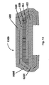
- Figure 12 is a schematic section through a simple tape sealed electro-optic display of the present invention.
- Figure 13 is a schematic section through a second tape sealed electro-optic display of the present invention in which the tape extends across the rear surface of the backplane.
- Figure 14 is a schematic section though a third tape sealed electro-optic display of the present invention.
- Figure 15 is a schematic section through a notionally tape sealed electro-optic displays of the present invention in which the tape seal is formed by extensions of the front substrate and adjacent adhesive layer of the display.
- Flexible, including rollable, electro-optic displays especially those using encapsulated electrophoretic media, present important new marketing opportunities; for example, large displays which can be stored in a compact form may be useful as additional display devices on electronic devices which are presently equipped only with a small display screen but where a larger display screen would often be useful; examples of such devices include cellular telephones equipped to receive electronic mail.
- flexible electro-optic displays will typically require sealing to prevent the ingress of water vapor and other environmental contaminants which can adversely affect the electro-optic properties or operating lifetime of the display.
- backplane is used herein consistent with its conventional meaning in the art of electro-optic displays and in the aforementioned patents and published applications, to mean a rigid or flexible material provided with one or more electrodes.
- the backplane may also be provided with electronics for addressing the display, or such electronics may be provided in a unit separate from the backplane.
- the backplane it is highly desirable that the backplane provide sufficient barrier properties to prevent ingress of moisture and other contaminants through the non-viewing side of the display (the display is of course normally viewed from the side remote from the backplane).
- barrier layers need to be added to the backplane to reduce ingress of moisture and other contaminants, the barrier layers should be located as closely as possible to the electro-optic layer so that little or no edge profile of low barrier material is present between the front (discussed below) and rear barrier layers.
- front substrate is used herein consistent with its conventional meaning in the art of electro-optic displays and in the aforementioned patents and published applications, to mean a rigid or flexible material that is light-transmissive (and preferably transparent).
- the front substrate will typically comprise at least one electrode, most commonly a single continuous front electrode extending across the entire display, although as already mentioned certain displays which are written with a stylus of similar writing implement separate from the display itself do not require a front electrode.
- the exposed surface of the front substrate will form the viewing surface through which an observer views the display, although, as in some of the preferred embodiments described below, there may be additional layers interposed between the front substrate and the viewing surface.
- the front substrate needs to provide sufficient barrier properties to prevent ingress of moisture and other contaminants through the viewing side of the display. If one or more additional layers need to be added to the front substrate to reduce ingress of moisture and other contaminants, the barrier layers should be located as closely as possible to the electro-optic layer so that little or no edge profile of low barrier material is present between the front and rear barrier layers.
- one preferred form of front substrate for electro-optic displays comprises a thin layer of ITO on PET, such coated films being readily available commercially.
- the ITO layer serves as a barrier material, but in practice inevitably suffers from pinholes and cracks, through which moisture and other contaminants can penetrate to the electro-optic material.
- a redundant barrier layer on to the front substrate, this redundant barrier layer being formed of a homopolymer (for example, polychlorotrifluoroethylene, available from Honeywell Corporation under the Registered Trade Mark “ACLAR”), or a sputtered ceramic (for example AIO x , available from Toppan Printing Company under the trade name Toppan GX Film).
- the redundant barrier layer should be thin to provide a flexible display, ideally about 12 ⁇ m, but could be as thick as 5 mil (127 ⁇ m) if sufficient flexibility is still available.
- the adhesive layer should be transparent, colorless, thin, flexible, have low creep (when the display is flexed or rolled), and be durable at all temperatures within the operating range of the display.
- Certain cross-linked polyurethanes and polyacrylates can be used as such adhesives.
- the barrier properties of a PET/ITO or similar front substrate may be improved by coating a redundant metal oxide layer (for example, an alumina layer) either on the opposed surface of the front substrate from the ITO layer or underneath the ITO layer.
- a redundant metal oxide layer for example, an alumina layer
- the combination of the ITO layer and the redundant metal oxide layer improves the barrier properties of the front substrate (for example by reducing migration of water vapor through the inevitable cracks and pinholes in the ITO layer) without undue yellowing of the substrate, such as would occur one attempted to improve barrier properties by increasing the thickness of the ITO layer.
- a more complex structure containing a ceramic material such as Barix (Registered Trade Mark) sealing material, available from Vitex Systems, Inc., 3047 Orchard Parkway, San Jose, CA 95134, United States of America could be used; again the barrier layer could be provided on the surface of the front substrate remote from the ITO layer or beneath the ITO layer.
- Vitex Systems currently sells a polymer film bearing both Barix and ITO layers under the trade name FlexGlass 200, but the polymeric film is 5 mil (127 ⁇ m) PEN.
- the barrier properties of the front substrate may also be controlled by careful choice of both the polymer and conductive material used in the front substrate.
- suitable polymers include PET, PEN, polycarbonate, poly(vinylidene chloride) (sold under the Registered Trade Mark “SARAN”), polychlorotrifluoroethylene (sold under the Registered Trade Marks “ACLAR” and “CLARIS”), triacetyl cellulose, the material sold under the Registered Trade Mark “ARTON” by JSR Company, polyethersulfone (PES) and laminates of two or more of these materials.
- Suitable transparent conductive materials include ITO, organic conductive polymers such as Baytron P (Registered Trade Mark), carbon nanotubes, and other suitably conducting light transmissive conductors (transmission greater than 60 per cent) having resistivities of less an about 10 4 ohms/square.
- the electro-optic layer may be an encapsulated electrophoretic layer, a polymer-dispersed electrophoretic layer, or any of the other types of electro-optic layer discussed above.
- the display may contain one or two lamination adhesive layers to attach the electro-optic material to the front substrate and/or the backplane.
- the display may be viewed through either lamination adhesive layer, and the display may be assembled by direct coating and lamination, or by the use of front plane laminates, inverted front plane laminates, or double release films, as described in the patents and applications mentioned in the "Reference to Related Applications" Section hereof.
- the display is normally viewed through the front substrate, in some cases a light-transmissive backplane can be used to provide a double-sided display, or one operating in the aforementioned shutter mode.
- the electro-optic displays are illustrated with the viewing surface (alternatively called the front surface) of the display at the top, so that references hereinafter to front and rear surfaces refer to upper and lower surfaces respectively as illustrated in the relevant drawings.
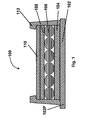
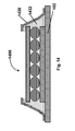
- FIG. 1 of the accompanying drawings is a schematic section through an overlapped sealing material display (generally designated 100) of the present invention.
- the display 100 comprises a flexible backplane 102, on which are disposed, in order, a lamination adhesive layer 104, a layer 106 of electro-optic material (illustrated as an encapsulated electrophoretic material comprising a plurality of capsules in a polymeric binder, but other types of electro-optic material could of course be used), a front substrate 108 comprising a PET film bearing, on its surface adjacent the electro-optic material layer 106, a thin layer of ITO (this ITO layer is not illustrated separately in Figure 1 ), and a protective or barrier layer 110 secured to the front substrate by a layer of optically clear adhesive (not shown).
- a layer of optically clear adhesive not shown.
- the layers 104-110 are all of the same size, which is smaller than the size of the backplane 102 (actually the layers 104-110 are smaller in both dimensions than the backplane 102, although this may not be apparent from Figure 1 ). Accordingly, a peripheral portion (designated 102P) of the backplane 102 extends outwardly beyond the edges of the layers 104-110 all around the periphery of these layers.
- An edge seal 112 is formed by dispensing a bead of a sealing material around the edge of the display 100, the edge seal 112 extending from the peripheral portion 102P of the backplane to the barrier layer 110, and overlapping a peripheral portion of the front surface of the barrier layer 110. It has been found that overlapping the edge seal over the front surface of the display in this manner is important in securing an edge seal having high mechanical durability.
- the material used to form the edge seal 112 may be any material that has sufficient flexibility, adhesion and barrier properties; obviously, it may be necessary to cure the sealing material after it has been applied.
- the display 100 shown in Figure 1 is a modified form of the electro-optic displays shown in Figures 11 , 12 , 13 and 15 of the aforementioned U.S. Patent 6,982,178 , differing only in the form of the edge seal; it has been found that the form of edge seal shown in Figure 1 gives better mechanical durability than the prior art edge seals.
- the display 100 may be constructed using the same methods as described in detail in the aforementioned U.S. Patent 6,982,178 .
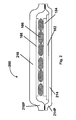
- FIG 2 is a schematic section through a double sealed protective sheet display (generally designated 200) of the present invention.
- This display 200 comprises a backplane 102, a lamination adhesive layer 104, a layer 106 of electro-optic material, and a front substrate 108, all of which are substantially the same as the corresponding integers of the display 100 shown in Figure 1 .
- the display 200 lacks the edge seal 112 of the display 100.
- the display 200 is provided with a front protective or barrier sheet 210 which serves the same protective and barrier function as the barrier layer 110 of display 100.
- the barrier sheet 210 shown in Figure 2 is substantially larger in both dimensions than the backplane 102 and the layers 104-108, so that a peripheral portion 210P of the barrier sheet 210 extends outwardly beyond the edges of the backplane 102 and the layers 104-108.
- the front barrier sheet 210 is adhesively secured to the front substrate 108 by an optically clear adhesive (not shown).
- the display 200 further comprises a rear barrier sheet 214, which is of the same size and material as the front barrier sheet 210.
- the rear barrier sheet 214 is adhesively secured to the backplane 102 by an adhesive (not shown); this adhesive may be, but does not need to be, optically clear since the adhesive is normally not visible to an observer of the display.
- a peripheral portion 214P of the rear barrier sheet 214 extends outwardly beyond the edges of the backplane 102 and lies the adjacent the peripheral portion 210P of the front barrier sheet 210, the two peripheral portions 210P and 214P being welded to each other all around the display 200, thus completely sealing the display 200. Laser or ultrasonic welding may be used, or the two peripheral portions could be adhesively secured together.
- the display 200 may offer manufacturing advantages, since the display 200 does not require accurate dispensing of a sealing material, but only welding or adhesion of two (typically polymeric) sheets, a process which can readily be effected in high volumes using apparatus and processes well known in the art.
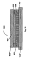
- FIG 3 is a schematic section through a single sealed protective sheet display (generally designated 300) of the present invention.
- This display 300 comprises a backplane 102', a lamination adhesive layer 104, a layer 106 of electro-optic material, and a front substrate 108, all of which are substantially the same as the corresponding integers of the display 200 shown in Figure 2 , except that the backplane 102' is thicker than the backplane 102 of the display 200 and may, for reasons explained below, include additional barrier layers, for example metal oxide layers on one or both of its major surfaces.
- the backplane 102' is also somewhat larger relative to the layers 104-108 than the backplane 102 of display 200, leaving a substantial peripheral portion 102P extending well beyond the edges of the layers 104-108.
- the display 300 further comprises a front protective or barrier sheet 310, which is similar to the barrier sheet 210 of display 200, and similarly has a peripheral portion 310P extending outwardly beyond the edges of the layers 104-108.
- the peripheral portion 310P of the front barrier sheet 310 is sealed to the peripheral portion 102P of the backplane 102' by melting an appropriate portion of the front barrier sheet using, for example, laser or ultrasonic welding.
- the peripheral portions 310P and 102P could be adhesively secured to each other.
- the single sealed protective sheet display 300 shown in Figure 3 is conceptually very similar to the double sealed protective sheet display 200 shown in Figure 2 , in that both types of displays sandwich the lamination adhesive layer, electro-optic layer and front substrate between two barrier layers, the difference between the two types of displays being that in the DSPS display the backplane and the rear barrier sheet are separate integers, whereas in the SSPS display the backplane serves both functions. Accordingly, the SSPS display places greater demands upon the barrier properties of the backplane than the DSPS display, and hence it may be desirable that an SSPS backplane include additional barrier layers, as already mentioned.
- the DSPS and SSPS types of display are especially adapted for use with flexible displays, in which the backplane is formed of flexible materials, for example polymeric films; in such a display the backplane might comprise, for example, organic transistors printed on a polymeric film.
- the backplane does not require the type of thick, rigid sealing member found in some prior art displays, and, provided the backplane is sufficiently flexible, the peripheral portions of the backplane and barrier sheet, or the two barrier sheets, adhered to each other can remain flexible.
- the present invention could be used in rigid or semi-rigid displays.
- FIG 4 is a schematic section through a "single protective sheet with sealer” (SPSS) display (generally designated 400) of the present invention which is a modified form of the display 300 shown in Figure 3 .
- the modification in display 400 consists of dispensing a bead 416 of sealing material extending from the peripheral portion of the backplane to the adjacent part of the front surface of the front barrier layer to provide additional barrier and mechanical protection to the display 400.
- the bead 416 covers the weld between the peripheral portions of the backplane and the front barrier sheet, and the overlap of the bead 416 over the front surface of the front barrier sheet forms a bond to the front barrier sheet for mechanical durability.
- the sealant material used to form the bead 416 may be any material that has sufficient flexibility, adhesion and barrier properties; it may of course be necessary to cure the sealant material after it is dispensed to form the bead 416.
- FIG. 5 shows a further modification of the display shown in Figure 4 .
- the SPSS display (generally designated 500) shown in Figure 5 differs from the display 400 shown in Figure 4 in that, in the display 500, the bead of sealant material is made thicker, so that it extends forwardly to the front surface of the front barrier layer, thus forming a modified bead designated 516, and an additional front protective sheet 518 having barrier problems is adhered to the front surface of the front protective sheet by means of an optically clear adhesive (not shown), the protective sheet 518 contacting the bead 516; thus, the bead 516 forms an "underfill" seal of the type described in the aforementioned U.S. Patent 6,982,178 .
- the sealant material used to form the bead 516 may be any material that has sufficient flexibility, adhesion and barrier properties; it may of course be necessary to cure the sealant material after it is dispensed to form the bead 516.
- the sealing of the electro-optic layer has been effected by various combinations of backplane, edge sealing material, and front and rear protective or barrier sheets.
- lamination adhesive layers it is also possible to use lamination adhesive layers to effect sealing of an electro-optic layer, and displays sealed in this manner will now be described.
- FIG. 6 is a schematic section through a double adhesive seal electro-optic display of this type.
- the display (generally designated 600) shown in Figure 6 comprises a backplane 102 and a first lamination adhesive layer 104, both of which are essentially identical to the corresponding integers in the displays shown in Figures 1 to 5 .
- the display 600 further comprises a layer 606 of electro-optic material, a second lamination adhesive layer 620 and a front substrate 608.
- the peripheral portions of the front substrate 608 and the second lamination adhesive layer 620 are deformed rearwardly relative to the central portions of these layers, so that the peripheral portion of the second lamination adhesive layer 620 contacts the first lamination adhesive layer 104, thus forming an edge seal, as indicated at 622.
- the double adhesive seal display 600 shown in Figure 6 may conveniently be formed using a double release film as described in the aforementioned 2004/0155857.
- Figure 7 is a schematic section through a display (generally designated 700), which is a modification of the display 600 shown in Figure 6 .
- the modification comprises providing an additional front protective sheet 718 (similar to the sheet 518 shown in Figure 5 ) and a bead 716 of sealing material (similar to the bead 516 shown in Figure 5 ), this bead 516 of sealing material extending from the backplane 102 to the rear surface of the protective sheet 718 and thus forming the same type of underfill seal as in Figure 5 .
- the remarks above regarding the properties needed in protective sheets and sealing materials also, of course, apply to the protective sheet 718 and sealing material 716.
- FIG 8 is a schematic section through a single adhesive seal electro-optic display (generally designated 800) of the present invention.
- the single adhesive seal (SAS) display 800 may notionally be regarded as produced by omitting the first lamination adhesive layer 104 from the display 600 shown in Figure 6 , and the numbering of the various layers in Figure 8 follows this assumed derivation of the display 800. Because the first lamination adhesive layer 104 is omitted from the display 800 the edge seal (indicated at 822) which seals the electro-optic layer 606 is formed between the lamination adhesive layer 620 and the backplane 102.
- the display 800 may conveniently be produced using an inverted front plane laminate as described in the aforementioned copending Application Serial No. 11/550,114 .
- FIG 9 is a schematic section through a first extended front substrate display (generally designated 900) of the present invention.
- the display 900 comprises a backplane 102, a first lamination adhesive layer 104, a layer 906 of electro-optic material, and a second lamination adhesive layer 920, all of which are essentially identical to the corresponding layers in the display 700 shown in Figure 7 , except that all the layers 104, 906 and 920 are of the same thickness throughout their areas, so that the front surface of the second lamination adhesive layer 920 lies parallel to the front surface of the backplane 102.
- the backplane 102 is larger in both dimensions than the layers 104, 906 and 920, so that a peripheral portion 102P of the backplane 102 extends outwardly beyond the edges of the layers 104, 906 and 920.
- the display 900 further comprises a front substrate 908, which is larger in both dimensions than the layers 104, 906 and 920, so that a peripheral portion 908P of the front substrate 908 extends outwardly beyond the edges of the layers 104, 906 and 920.
- a sealing gasket 926 which may either be printed on to the backplane 102 or front substrate 908 before the two are laminated together, or may be dispensed at the required location as previously described, extends from the peripheral portion 102P of the backplane to the peripheral portion 908P of the front substrate, thus sealing the display.
- FIG 10 is a schematic section through a second extended front substrate electro-optic display (generally designated 1000) of the present invention.
- the display 1000 may notionally be regarded as a modified form of the display 900 shown in Figure 9 , the modification comprising the removal of the first lamination adhesive layer 104 from the display 900, so that in the display 1000 the electro-optic layer 906 is in direct contact with the backplane 102.
- FIG 11 is a schematic section through a third extended front substrate display (generally designated 1100) of the present invention which is essentially a modified form of the display 1000 shown in Figure 10 , the modification being generally similar to that used to modify the display 600 shown in Figure 6 to the display 700 shown in Figure 7 .
- the display 1100 may be regarded as notionally produced from the display 1000 by securing a front protective sheet 1118 with an optically clear adhesive (not shown) to the front surface of the front substrate 908, and extending the sealing gasket outwardly and forwardly around the edges of the front substrate 908 to form a modified gasket 926', which extends from the backplane 102 to the rear surface of the front protective sheet 1118, thus providing additional sealing of the display 1100.
- the gasket 926' may be a printed gasket, although in view of its form, it may be more convenient to produce it by dispensing sealing material around the periphery of display 1100 after the front protective layer 1118 is in place.
- FIG. 12 is a schematic section through a display (generally designated 1200) of this type.
- the display 1200 comprises a backplane 102, a lamination adhesive layer 104, a layer 106 of electro-optic material and a front substrate 108, all of which are essentially identical to the corresponding integers of the display 100 shown in Figure 1 .
- the display 1200 is sealed by means of a flexible tape 1230, which extends all around the periphery of the display 1200.
- the tape 1230 in fact comprises two separate layers, an outer layer having good barrier characteristics (typically a polymer, for example polychlorotrifluoroethylene) and an inner adhesive layer, which is used to secure the tape to the backplane and front substrate of the display.
- an outer layer having good barrier characteristics typically a polymer, for example polychlorotrifluoroethylene
- an inner adhesive layer which is used to secure the tape to the backplane and front substrate of the display.
- the tape is adhesively secured to the rear surface of the backplane 102 and the front surface of the front substrate 108, thus forming a complete seal around the display, and eliminating the need for any outward extension of the front substrate similar to that shown in Figure 11 .
- FIG 13 is a schematic section through a second tape sealed display (generally designated 1300) which is a modified form of the display 1200 shown in Figure 12 .
- the tape 1230 is carried across the entire rear surface of the backplane as a portion designated 1230R.
- the display 1300 is normally produced by placing the backplane 102, already carrying the layers 104-108, on to an adhesive barrier sheet, and then folding peripheral portions of the barrier sheet around the edges of the display to form the tape seal.
- FIG 14 is a schematic section through another electro-optic display (generally designated 1400) which may notionally be regarded as a tape sealed display, although in practice it will typically not be produced using a preformed tape.
- the display 1400 has a backplane 102, lamination adhesive layer, electro-optic layer and front substrate essentially identical to the display 1300 shown in Figure 13 except that the backplane 102 is enlarged to that a peripheral portion thereof extends beyond the periphery of the other layers.
- a flexible protective layer or tape 1430 extends from the peripheral portion of the backplane 102 and overlaps the front surface of the front substrate, while a flexible sealant 1432 underlies the tape 1430 and secures the tape to the other parts of the display 1400. Note that the flexible sealant 1432 also overlaps the front surface of the front substrate. In this type of display, it is important that the flexible sealant 1432 as well as the tape 1430 have the desired barrier properties, in particular a low water vapor transmission rate.
- the display 1400 will typically be produced by arranging the backplane, lamination adhesive layer, electro-optic layer and front substrate in their correct relative positions, dispensing a bead of the flexible sealant around the edges of the assembled layers, and applying the flexible tape over the bead of sealing, thereby forming the sealant into the shape shown in Figure 14 .
- FIG 15 is a schematic section through another electro-optic display (generally designated 1500) which may notionally be regarded as a tape sealed display, although in practice it will typically not be produced using a preformed tape.
- the display 1500 may be regarded as a modification of the display 600 shown in Figure 6 , and like the display 600 the display 1500 comprises a backplane 102, a first lamination adhesive layer 104, an electro-optic layer 606, a second lamination adhesive layer 620 and a front substrate 608, although, as will readily be apparent from Figure 15 , the exact forms of these layers differ somewhat from those of the display 600.
- the front substrate 608 and the second lamination adhesive layer 620 are provided with extensions (designated 608E and 620E respectively) which are wrapped around the edges of the electro-optic layer 606, the first lamination adhesive layer 104 and the backplane 102, so that both extensions overlap a peripheral portion of the rear surface of the backplane 102; thus, the extensions 608E and 620E act to seal the electro-optic display in a manner rather similar to the tape 1230 shown in Figure 12 .
- the electrode arrangements in the various types of displays of the present invention can be of any of the types described in the aforementioned E Ink and MIT patents and applications.
- the displays may be of the direct drive type, in which the backplane is provided with a plurality of electrodes, each of which is provided with a separate connector by means of a which a controller can control the voltage applied to the specific electrode.
- a single continuous front electrode is usually provided covering the whole display, although other front electrode arrangements are possible.
- the backplane carries a plurality of elongate parallel electrodes ("column electrodes”), while on the opposed side of the electro-optic material there is provided a plurality of elongate parallel electrodes (“row electrodes”) running at right angles to the column electrodes, the overlap between one specific column electrode and one specific row electrode defining one pixel of the display.
- the present displays may also be of the active matrix type, typically with a single continuous front electrode covering the whole display and a matrix of pixel electrodes on the backplane, each pixel electrode defining one pixel of the display and having an associated transistor or other non-linear element, the active matrix display being scanned in the conventional manner to write the display in a row-by-row fashion.
- the present display may also be of the stylus-driven type, with (typically) a single electrode on the backplane and no permanent front electrode, writing of the display being effected by moving a stylus across the front surface of the display.
- the displays of the present invention may be used in any application in which prior art electro-optic displays have been used.
- the present displays may be used in electronic book readers, portable computers, tablet computers, cellular telephones, smart cards, signs, watches, shelf labels and flash drives.
Landscapes
- Physics & Mathematics (AREA)
- Nonlinear Science (AREA)
- General Physics & Mathematics (AREA)
- Optics & Photonics (AREA)
- Chemical & Material Sciences (AREA)
- Chemical Kinetics & Catalysis (AREA)
- Health & Medical Sciences (AREA)
- Life Sciences & Earth Sciences (AREA)
- Electrochemistry (AREA)
- Molecular Biology (AREA)
- Crystallography & Structural Chemistry (AREA)
- Mathematical Physics (AREA)
- Electrochromic Elements, Electrophoresis, Or Variable Reflection Or Absorption Elements (AREA)
- Devices For Indicating Variable Information By Combining Individual Elements (AREA)
Applications Claiming Priority (2)
| Application Number | Priority Date | Filing Date | Title |
|---|---|---|---|
| US11/612,732 US7649674B2 (en) | 2002-06-10 | 2006-12-19 | Electro-optic display with edge seal |
| EP06851517.0A EP2104876B2 (fr) | 2006-12-19 | 2007-08-08 | Affichage électro-optique avec joint de bordure |
Related Parent Applications (2)
| Application Number | Title | Priority Date | Filing Date |
|---|---|---|---|
| EP06851517.0 Division | 2007-08-08 | ||
| EP06851517.0A Division-Into EP2104876B2 (fr) | 2006-12-19 | 2007-08-08 | Affichage électro-optique avec joint de bordure |
Publications (2)
| Publication Number | Publication Date |
|---|---|
| EP2546693A2 true EP2546693A2 (fr) | 2013-01-16 |
| EP2546693A3 EP2546693A3 (fr) | 2013-04-10 |
Family
ID=38223843
Family Applications (2)
| Application Number | Title | Priority Date | Filing Date |
|---|---|---|---|
| EP12006356.5A Withdrawn EP2546693A3 (fr) | 2006-12-19 | 2007-08-08 | Dispositif d'affichage électro-optique avec joint de bordure |
| EP06851517.0A Active EP2104876B2 (fr) | 2006-12-19 | 2007-08-08 | Affichage électro-optique avec joint de bordure |
Family Applications After (1)
| Application Number | Title | Priority Date | Filing Date |
|---|---|---|---|
| EP06851517.0A Active EP2104876B2 (fr) | 2006-12-19 | 2007-08-08 | Affichage électro-optique avec joint de bordure |
Country Status (4)
| Country | Link |
|---|---|
| US (7) | US7649674B2 (fr) |
| EP (2) | EP2546693A3 (fr) |
| KR (7) | KR101689942B1 (fr) |
| WO (1) | WO2008088315A2 (fr) |
Cited By (1)
| Publication number | Priority date | Publication date | Assignee | Title |
|---|---|---|---|---|
| CN109799663A (zh) * | 2019-01-25 | 2019-05-24 | 中山大学 | 基于可拉伸衬底的电子纸产品及其封装方法 |
Families Citing this family (239)
| Publication number | Priority date | Publication date | Assignee | Title |
|---|---|---|---|---|
| US7583251B2 (en) | 1995-07-20 | 2009-09-01 | E Ink Corporation | Dielectrophoretic displays |
| US7999787B2 (en) | 1995-07-20 | 2011-08-16 | E Ink Corporation | Methods for driving electrophoretic displays using dielectrophoretic forces |
| US7848006B2 (en) | 1995-07-20 | 2010-12-07 | E Ink Corporation | Electrophoretic displays with controlled amounts of pigment |
| US8040594B2 (en) | 1997-08-28 | 2011-10-18 | E Ink Corporation | Multi-color electrophoretic displays |
| EP1093600B1 (fr) * | 1998-07-08 | 2004-09-15 | E Ink Corporation | Procedes permettant d'ameliorer la couleur des dispositifs electrophoretiques microencapsules |
| AU2002250304A1 (en) * | 2001-03-13 | 2002-09-24 | E Ink Corporation | Apparatus for displaying drawings |
| US8390918B2 (en) | 2001-04-02 | 2013-03-05 | E Ink Corporation | Electrophoretic displays with controlled amounts of pigment |
| US7679814B2 (en) | 2001-04-02 | 2010-03-16 | E Ink Corporation | Materials for use in electrophoretic displays |
| US7223672B2 (en) * | 2002-04-24 | 2007-05-29 | E Ink Corporation | Processes for forming backplanes for electro-optic displays |
| US7583427B2 (en) | 2002-06-10 | 2009-09-01 | E Ink Corporation | Components and methods for use in electro-optic displays |
| US7649674B2 (en) | 2002-06-10 | 2010-01-19 | E Ink Corporation | Electro-optic display with edge seal |
| US8363299B2 (en) * | 2002-06-10 | 2013-01-29 | E Ink Corporation | Electro-optic displays, and processes for the production thereof |
| US8049947B2 (en) | 2002-06-10 | 2011-11-01 | E Ink Corporation | Components and methods for use in electro-optic displays |
| US20040031167A1 (en) * | 2002-06-13 | 2004-02-19 | Stein Nathan D. | Single wafer method and apparatus for drying semiconductor substrates using an inert gas air-knife |
| US7839564B2 (en) * | 2002-09-03 | 2010-11-23 | E Ink Corporation | Components and methods for use in electro-optic displays |
| US20130063333A1 (en) | 2002-10-16 | 2013-03-14 | E Ink Corporation | Electrophoretic displays |
| US20170052422A1 (en) * | 2002-11-26 | 2017-02-23 | E Ink Corporation | Flexible electronic circuits and displays |
| US7910175B2 (en) | 2003-03-25 | 2011-03-22 | E Ink Corporation | Processes for the production of electrophoretic displays |
| US20110164301A1 (en) | 2003-11-05 | 2011-07-07 | E Ink Corporation | Electro-optic displays, and materials for use therein |
| US8177942B2 (en) * | 2003-11-05 | 2012-05-15 | E Ink Corporation | Electro-optic displays, and materials for use therein |
| US7551346B2 (en) | 2003-11-05 | 2009-06-23 | E Ink Corporation | Electro-optic displays, and materials for use therein |
| US8405193B2 (en) * | 2004-04-02 | 2013-03-26 | General Electric Company | Organic electronic packages having hermetically sealed edges and methods of manufacturing such packages |
| US11250794B2 (en) | 2004-07-27 | 2022-02-15 | E Ink Corporation | Methods for driving electrophoretic displays using dielectrophoretic forces |
| EP1856571B1 (fr) * | 2005-02-28 | 2009-12-30 | Koninklijke Philips Electronics N.V. | Dispositif d'affichage |
| US20060278965A1 (en) * | 2005-06-10 | 2006-12-14 | Foust Donald F | Hermetically sealed package and methods of making the same |
| JP5239152B2 (ja) * | 2006-02-02 | 2013-07-17 | セイコーエプソン株式会社 | 電気光学装置の製造方法、及び電子機器 |
| US8390301B2 (en) | 2006-03-08 | 2013-03-05 | E Ink Corporation | Electro-optic displays, and materials and methods for production thereof |
| US7733554B2 (en) * | 2006-03-08 | 2010-06-08 | E Ink Corporation | Electro-optic displays, and materials and methods for production thereof |
| US7843624B2 (en) | 2006-03-08 | 2010-11-30 | E Ink Corporation | Electro-optic displays, and materials and methods for production thereof |
| US8610988B2 (en) * | 2006-03-09 | 2013-12-17 | E Ink Corporation | Electro-optic display with edge seal |
| US7952790B2 (en) | 2006-03-22 | 2011-05-31 | E Ink Corporation | Electro-optic media produced using ink jet printing |
| DE102007029066B4 (de) * | 2006-06-21 | 2013-01-03 | Flabeg Gmbh & Co. Kg | Elektrisch aktives Element |
| US7903319B2 (en) | 2006-07-11 | 2011-03-08 | E Ink Corporation | Electrophoretic medium and display with improved image stability |
| US8018640B2 (en) | 2006-07-13 | 2011-09-13 | E Ink Corporation | Particles for use in electrophoretic displays |
| US20080024429A1 (en) * | 2006-07-25 | 2008-01-31 | E Ink Corporation | Electrophoretic displays using gaseous fluids |
| US7492497B2 (en) | 2006-08-02 | 2009-02-17 | E Ink Corporation | Multi-layer light modulator |
| EP2064581A4 (fr) | 2006-09-20 | 2011-01-26 | E Ink Corp | Composants et procédés d'utilisation de ceux-ci dans des écrans électro-optiques |
| US7649666B2 (en) | 2006-12-07 | 2010-01-19 | E Ink Corporation | Components and methods for use in electro-optic displays |
| US7688497B2 (en) * | 2007-01-22 | 2010-03-30 | E Ink Corporation | Multi-layer sheet for use in electro-optic displays |
| WO2008091850A2 (fr) | 2007-01-22 | 2008-07-31 | E Ink Corporation | Feuille à plusieurs couches destinée à être utilisée dans des afficheurs électro-optiques |
| US7826129B2 (en) | 2007-03-06 | 2010-11-02 | E Ink Corporation | Materials for use in electrophoretic displays |
| CN101681211A (zh) * | 2007-05-21 | 2010-03-24 | 伊英克公司 | 用于驱动视频电光显示器的方法 |
| WO2009006248A1 (fr) | 2007-06-29 | 2009-01-08 | E Ink Corporation | Dispositifs d'affichage électro-optiques, et matériaux et procédé pour la production de ceux-ci |
| US8902153B2 (en) | 2007-08-03 | 2014-12-02 | E Ink Corporation | Electro-optic displays, and processes for their production |
| US20090122389A1 (en) | 2007-11-14 | 2009-05-14 | E Ink Corporation | Electro-optic assemblies, and adhesives and binders for use therein |
| WO2009072226A1 (fr) | 2007-12-06 | 2009-06-11 | Sharp Kabushiki Kaisha | Dispositif d'affichage souple |
| US8054526B2 (en) | 2008-03-21 | 2011-11-08 | E Ink Corporation | Electro-optic displays, and color filters for use therein |
| US8314784B2 (en) * | 2008-04-11 | 2012-11-20 | E Ink Corporation | Methods for driving electro-optic displays |
| GB0811058D0 (en) * | 2008-06-17 | 2008-07-23 | Pilkington Group Ltd | Sealed switchable glazing |
| JP2011003522A (ja) | 2008-10-16 | 2011-01-06 | Semiconductor Energy Lab Co Ltd | フレキシブル発光装置、電子機器及びフレキシブル発光装置の作製方法 |
| TWI484273B (zh) * | 2009-02-09 | 2015-05-11 | E Ink Corp | 電泳粒子 |
| US8098418B2 (en) | 2009-03-03 | 2012-01-17 | E. Ink Corporation | Electro-optic displays, and color filters for use therein |
| US20100230044A1 (en) * | 2009-03-12 | 2010-09-16 | Shih-Kang Fan | Bubbleless packaging method |
| US8754859B2 (en) | 2009-10-28 | 2014-06-17 | E Ink Corporation | Electro-optic displays with touch sensors and/or tactile feedback |
| US8654436B1 (en) | 2009-10-30 | 2014-02-18 | E Ink Corporation | Particles for use in electrophoretic displays |
| JP5638229B2 (ja) * | 2009-11-25 | 2014-12-10 | 大日本印刷株式会社 | ツイストボール型電子ペーパー |
| KR101681128B1 (ko) | 2010-01-21 | 2016-12-02 | 삼성디스플레이 주식회사 | 표시 패널 및 이의 제조 방법 |
| EP2553522B1 (fr) | 2010-04-02 | 2016-03-23 | E-Ink Corporation | Milieux d'électrophorèse |
| TWI484275B (zh) | 2010-05-21 | 2015-05-11 | E Ink Corp | 光電顯示器及其驅動方法、微型空腔電泳顯示器 |
| TWI451371B (zh) | 2010-05-21 | 2014-09-01 | Au Optronics Corp | 顯示裝置 |
| TWI414821B (zh) * | 2010-06-04 | 2013-11-11 | Au Optronics Corp | 電子墨水顯示器及其製造方法 |
| US9935289B2 (en) | 2010-09-10 | 2018-04-03 | Industrial Technology Research Institute Institute | Environmental sensitive element package and encapsulation method thereof |
| US20120068934A1 (en) * | 2010-09-17 | 2012-03-22 | Microsoft Corporation | Interactive keyboard with viewable display |
| TWI421611B (zh) | 2010-10-08 | 2014-01-01 | Au Optronics Corp | 電泳顯示結構 |
| TWI427389B (zh) * | 2010-10-22 | 2014-02-21 | Au Optronics Corp | 拼接式電泳顯示面板 |
| TWI434250B (zh) | 2010-12-15 | 2014-04-11 | Au Optronics Corp | 可撓性顯示面板 |
| KR20120071751A (ko) * | 2010-12-23 | 2012-07-03 | 엘지디스플레이 주식회사 | 디스플레이 장치 |
| TWI419097B (zh) * | 2011-01-11 | 2013-12-11 | E Ink Holdings Inc | 顯示器 |
| US9087488B1 (en) | 2011-09-15 | 2015-07-21 | Amazon Technologies, Inc. | Producing electro-optic display with seamless front surface |
| US10190743B2 (en) | 2012-04-20 | 2019-01-29 | E Ink Corporation | Illumination systems for reflective displays |
| US11467466B2 (en) | 2012-04-20 | 2022-10-11 | E Ink Corporation | Illumination systems for reflective displays |
| US9847512B2 (en) | 2012-12-22 | 2017-12-19 | Industrial Technology Research Institute | Electronic device package structure and manufacturing method thereof |
| KR102018178B1 (ko) * | 2013-01-07 | 2019-09-04 | 엘지디스플레이 주식회사 | 디스펜싱 가능한 전기 영동 유체를 포함하는 광 제어기 및 그 제조 방법 |
| US9715155B1 (en) | 2013-01-10 | 2017-07-25 | E Ink Corporation | Electrode structures for electro-optic displays |
| US9726957B2 (en) | 2013-01-10 | 2017-08-08 | E Ink Corporation | Electro-optic display with controlled electrochemical reactions |
| CA2902240C (fr) * | 2013-02-24 | 2019-06-18 | Esmaeil Banaei | Procede d'etirage thermique de toles structurees |
| CN110515251A (zh) * | 2013-03-07 | 2019-11-29 | 思维奇材料公司 | 包封的可转换膜、密封的膜和形成其的方法 |
| KR20180133562A (ko) | 2013-04-15 | 2018-12-14 | 가부시키가이샤 한도오따이 에네루기 켄큐쇼 | 발광 장치 |
| TWI515937B (zh) | 2013-05-15 | 2016-01-01 | 緯創資通股份有限公司 | 有機光電元件之封裝結構以及封裝方法 |
| US9269914B2 (en) | 2013-08-01 | 2016-02-23 | Semiconductor Energy Laboratory Co., Ltd. | Light-emitting device, electronic device, and lighting device |
| US10726760B2 (en) | 2013-10-07 | 2020-07-28 | E Ink California, Llc | Driving methods to produce a mixed color state for an electrophoretic display |
| TWI550332B (zh) | 2013-10-07 | 2016-09-21 | 電子墨水加利福尼亞有限責任公司 | 用於彩色顯示裝置的驅動方法 |
| US10380931B2 (en) | 2013-10-07 | 2019-08-13 | E Ink California, Llc | Driving methods for color display device |
| WO2015089663A1 (fr) | 2013-12-19 | 2015-06-25 | Switch Materials Inc. | Objets commutables et procédés de fabrication |
| CN109491173B (zh) | 2014-01-17 | 2022-07-12 | 伊英克公司 | 具有双相电极层的电光显示器 |
| US10317767B2 (en) | 2014-02-07 | 2019-06-11 | E Ink Corporation | Electro-optic display backplane structure with drive components and pixel electrodes on opposed surfaces |
| HK1225848A1 (zh) | 2014-02-07 | 2017-09-15 | 伊英克公司 | 电光显示器的背板结构 |
| US10446585B2 (en) * | 2014-03-17 | 2019-10-15 | E Ink Corporation | Multi-layer expanding electrode structures for backplane assemblies |
| JP6375730B2 (ja) * | 2014-07-02 | 2018-08-22 | 凸版印刷株式会社 | 表示装置 |
| US10054716B2 (en) * | 2014-09-29 | 2018-08-21 | Buwon Precision Sciences Co., Ltd. | Strengthened cover lens and method for strengthening cover lens |
| WO2016059514A1 (fr) | 2014-10-17 | 2016-04-21 | Semiconductor Energy Laboratory Co., Ltd. | Dispositif électronique |
| WO2016059497A1 (fr) | 2014-10-17 | 2016-04-21 | Semiconductor Energy Laboratory Co., Ltd. | Dispositif électroluminescent, module, dispositif électronique, et procédé de fabrication de dispositif électroluminescent |
| JP2016085457A (ja) | 2014-10-24 | 2016-05-19 | 株式会社半導体エネルギー研究所 | 電子機器 |
| CN113341627B (zh) | 2014-11-07 | 2024-08-20 | 伊英克公司 | 电光显示器的应用 |
| US11435610B2 (en) | 2014-11-17 | 2022-09-06 | Alphamicron Incorporated | Method for producing a flexible electro-optic cell |
| KR102413786B1 (ko) | 2014-11-17 | 2022-06-28 | 알파마이크론, 인크. | 가요성 전기-광학 셀의 생산 방법 |
| US10914991B2 (en) | 2014-11-17 | 2021-02-09 | Alphamicron Incorporated | Method for producing a flexible electro-optic cell |
| KR102326672B1 (ko) | 2014-12-23 | 2021-11-16 | 삼성전자 주식회사 | 데이터 통신이 가능한 전자장치 및 그 충전방법 |
| TWI631406B (zh) | 2015-01-05 | 2018-08-01 | 美商電子墨水股份有限公司 | 光電顯示器 |
| US10197883B2 (en) | 2015-01-05 | 2019-02-05 | E Ink Corporation | Electro-optic displays, and methods for driving same |
| US9835925B1 (en) | 2015-01-08 | 2017-12-05 | E Ink Corporation | Electro-optic displays, and processes for the production thereof |
| US9847509B2 (en) | 2015-01-22 | 2017-12-19 | Industrial Technology Research Institute | Package of flexible environmental sensitive electronic device and sealing member |
| US9684339B2 (en) | 2015-02-03 | 2017-06-20 | Microsoft Technology Licensing, Llc | Bendable display assembly |
| US20160226015A1 (en) * | 2015-02-03 | 2016-08-04 | Microsoft Technology Licensing, Llc | Edge sealing for bendable device |
| PL3254275T3 (pl) | 2015-02-04 | 2023-10-02 | E Ink Corporation | Wyświetlacze elektrooptyczne wyświetlające w trybie ciemnym i w trybie jasnym oraz powiązane urządzenie i sposoby |
| US9589895B2 (en) * | 2015-04-15 | 2017-03-07 | Globalfoundries Inc. | Whole wafer edge seal |
| US10997930B2 (en) | 2015-05-27 | 2021-05-04 | E Ink Corporation | Methods and circuitry for driving display devices |
| WO2017004176A1 (fr) | 2015-06-29 | 2017-01-05 | E Ink Corporation | Procédé de raccordement mécanique et électrique à des électrodes d'affichage |
| ES2974101T3 (es) | 2015-06-30 | 2024-06-25 | E Ink Corp | Pantallas electroforéticas compuestas |
| KR102632066B1 (ko) * | 2015-07-30 | 2024-02-02 | 가부시키가이샤 한도오따이 에네루기 켄큐쇼 | 발광 장치의 제작 방법, 발광 장치, 모듈, 및 전자 기기 |
| US20190205077A1 (en) * | 2015-08-19 | 2019-07-04 | E Ink Corporation | Displays intended for use in architectural applications |
| US11087644B2 (en) | 2015-08-19 | 2021-08-10 | E Ink Corporation | Displays intended for use in architectural applications |
| US20170052753A1 (en) * | 2015-08-19 | 2017-02-23 | E Ink Corporation | Displays intended for use in architectural applications |
| CN107924100B (zh) | 2015-08-31 | 2021-03-23 | 伊英克公司 | 电子地擦除绘图装置 |
| EP3350798B1 (fr) | 2015-09-16 | 2023-07-26 | E Ink Corporation | Appareil et procédés pour piloter des dispositifs d'affichage |
| US10803813B2 (en) | 2015-09-16 | 2020-10-13 | E Ink Corporation | Apparatus and methods for driving displays |
| US11657774B2 (en) | 2015-09-16 | 2023-05-23 | E Ink Corporation | Apparatus and methods for driving displays |
| US10062337B2 (en) | 2015-10-12 | 2018-08-28 | E Ink California, Llc | Electrophoretic display device |
| WO2017087747A1 (fr) | 2015-11-18 | 2017-05-26 | E Ink Corporation | Affichages électro-optiques |
| JP2019507462A (ja) * | 2015-12-28 | 2019-03-14 | スリーエム イノベイティブ プロパティズ カンパニー | 流体キャビティ構成を有する可撓性電子デバイス |
| KR102505878B1 (ko) | 2016-01-29 | 2023-03-06 | 삼성디스플레이 주식회사 | 플렉서블 디스플레이 장치 |
| US10276109B2 (en) | 2016-03-09 | 2019-04-30 | E Ink Corporation | Method for driving electro-optic displays |
| US10593272B2 (en) | 2016-03-09 | 2020-03-17 | E Ink Corporation | Drivers providing DC-balanced refresh sequences for color electrophoretic displays |
| CN107290914B (zh) * | 2016-04-01 | 2022-09-09 | 上海伯乐电子有限公司 | 电子纸显示模组及其制备方法、电子纸显示装置 |
| PT3465628T (pt) | 2016-05-24 | 2020-07-24 | E Ink Corp | Método para reprodução de imagens de cor |
| HK1258890A1 (zh) | 2016-05-31 | 2019-11-22 | 伊英克公司 | 用於电光显示器的背板 |
| WO2017209869A2 (fr) | 2016-05-31 | 2017-12-07 | E Ink Corporation | Affichages électro-optiques étirables |
| WO2017214508A1 (fr) | 2016-06-10 | 2017-12-14 | E Ink Corporation | Appareil d'affichage électro-optique |
| CN108063906B (zh) * | 2016-11-07 | 2020-10-30 | 鸿富锦精密工业(深圳)有限公司 | 超薄电视 |
| WO2018160546A1 (fr) | 2017-02-28 | 2018-09-07 | E Ink Corporation | Dispositifs d'affichage électrophorétiques inscriptibles comprenant des circuits de détection et des stylets configurés pour interagir avec des circuits de détection |
| CA3200340A1 (fr) | 2017-03-06 | 2018-09-13 | E Ink Corporation | Procede permettant de restituer des images en couleurs |
| EP3602193A4 (fr) | 2017-03-28 | 2021-01-06 | E Ink Corporation | Fond de panier poreux pour écran électro-optique |
| CN115148163B (zh) | 2017-04-04 | 2023-09-05 | 伊英克公司 | 用于驱动电光显示器的方法 |
| PL3610323T3 (pl) | 2017-04-12 | 2021-04-19 | Saint-Gobain Glass France | Szyba wielowarstwowa z elementem funkcjonalnym o właściwościach optycznych sterowalnych elektrycznie |
| WO2018213687A2 (fr) | 2017-05-19 | 2018-11-22 | E Ink Corporation | Écran électro-optique pliable comprenant une numérisation et une activation par pression |
| EP3631575A4 (fr) | 2017-05-30 | 2021-01-13 | E Ink Corporation | Afficheurs électro-optiques |
| US11404013B2 (en) | 2017-05-30 | 2022-08-02 | E Ink Corporation | Electro-optic displays with resistors for discharging remnant charges |
| CN107167981A (zh) * | 2017-06-01 | 2017-09-15 | 广州奥熠电子科技有限公司 | 一种电光显示组件及其制造方法 |
| KR20240064046A (ko) * | 2017-07-31 | 2024-05-10 | 다이니폰 인사츠 가부시키가이샤 | 접합 유리, 접합 유리의 제조 방법 |
| CN111133501A (zh) | 2017-09-12 | 2020-05-08 | 伊英克公司 | 用于驱动电光显示器的方法 |
| US11721295B2 (en) | 2017-09-12 | 2023-08-08 | E Ink Corporation | Electro-optic displays, and methods for driving same |
| WO2019077920A1 (fr) * | 2017-10-17 | 2019-04-25 | ソニー株式会社 | Dispositif de gradation, dispositif d'affichage d'image, dispositif d'affichage de production de dispositif de gradation |
| CA3075408C (fr) | 2017-10-18 | 2022-06-28 | E Ink Corporation | Dispositifs microfluidiques numeriques comprenant des substrats doubles a transistors en couches minces et detection capacitive |
| US10824042B1 (en) | 2017-10-27 | 2020-11-03 | E Ink Corporation | Electro-optic display and composite materials having low thermal sensitivity for use therein |
| CN111226163B (zh) | 2017-11-03 | 2021-10-22 | 伊英克公司 | 用于生产电光显示器的工艺 |
| CN111492307A (zh) | 2017-12-19 | 2020-08-04 | 伊英克公司 | 电光显示器的应用 |
| JP7177158B2 (ja) | 2017-12-22 | 2022-11-22 | イー インク コーポレイション | 電気光学ディスプレイ及びこれを駆動するための方法 |
| EP3743909A4 (fr) | 2018-01-22 | 2021-08-18 | E Ink Corporation | Dispositifs d'affichage électro-optiques et leurs procédés d'excitation |
| CN111712759A (zh) | 2018-02-15 | 2020-09-25 | 伊英克公司 | 具有t线和像素电极之间的减小的电容耦合的窄边框电光显示器背板的通孔布局 |
| US11175561B1 (en) | 2018-04-12 | 2021-11-16 | E Ink Corporation | Electrophoretic display media with network electrodes and methods of making and using the same |
| TWI707178B (zh) | 2018-05-17 | 2020-10-11 | 美商伊英克加利福尼亞有限責任公司 | 電光顯示器及製造顯示器的方法 |
| US11643494B2 (en) | 2018-07-12 | 2023-05-09 | 3M Innovative Properties Company | Composition comprising styrene isobutylene block copolymer and ethylenically unsaturated monomer |
| WO2020018508A1 (fr) | 2018-07-17 | 2020-01-23 | E Ink California, Llc | Dispositifs d'affichage électro-optiques et procédés de commande |
| JP7108779B2 (ja) | 2018-08-10 | 2022-07-28 | イー インク カリフォルニア, エルエルシー | 反射体を伴う切り替え可能な光コリメート層 |
| US11397366B2 (en) | 2018-08-10 | 2022-07-26 | E Ink California, Llc | Switchable light-collimating layer including bistable electrophoretic fluid |
| KR102521144B1 (ko) | 2018-08-10 | 2023-04-12 | 이 잉크 캘리포니아 엘엘씨 | 쌍안정 전기영동 유체를 포함하는 전환가능한 광 시준층에 대한 구동 파형들 |
| US11353759B2 (en) | 2018-09-17 | 2022-06-07 | Nuclera Nucleics Ltd. | Backplanes with hexagonal and triangular electrodes |
| KR102577837B1 (ko) | 2018-10-15 | 2023-09-12 | 이 잉크 코포레이션 | 디지털 미세유체 전달 디바이스 |
| CN109300400A (zh) * | 2018-10-31 | 2019-02-01 | 上海天马微电子有限公司 | 显示面板及显示装置 |
| CN118348719A (zh) | 2018-11-09 | 2024-07-16 | 伊英克公司 | 电光显示器 |
| EP3888079A4 (fr) | 2018-11-30 | 2022-08-24 | E Ink California, LLC | Écrans électro-optiques et procédés de pilotage |
| WO2020122917A1 (fr) | 2018-12-13 | 2020-06-18 | E Ink Corporation | Systèmes d'éclairage pour affichages réfléchissants |
| US11521565B2 (en) | 2018-12-28 | 2022-12-06 | E Ink Corporation | Crosstalk reduction for electro-optic displays |
| KR102647463B1 (ko) | 2018-12-30 | 2024-03-13 | 이 잉크 코포레이션 | 전기 광학 디스플레이들 |
| CN114270254B (zh) * | 2019-08-26 | 2025-07-25 | 伊英克公司 | 包含识别标记的电光装置 |
| CN114641820B (zh) | 2019-11-14 | 2024-01-05 | 伊英克公司 | 用于驱动电光显示器的方法 |
| WO2021101859A1 (fr) | 2019-11-18 | 2021-05-27 | E Ink Corporation | Procédés de commande de dispositifs d'affichages électrooptiques |
| EP4100791A4 (fr) | 2020-02-07 | 2024-03-06 | E Ink Corporation | Couche d'affichage électrophorétique à électrode supérieure en film mince |
| CN113269291B (zh) * | 2020-02-14 | 2025-03-14 | 汉朔科技股份有限公司 | 电子货架标签及其制造方法 |
| CN113625500B (zh) * | 2020-04-21 | 2024-04-16 | 元太科技工业股份有限公司 | 电子纸封装结构 |
| TWI731655B (zh) * | 2020-04-21 | 2021-06-21 | 元太科技工業股份有限公司 | 電子紙封裝結構 |
| CN111443545B (zh) * | 2020-05-12 | 2025-09-05 | 深圳市光羿科技有限公司 | 一种边缘密封导电基体与电致变色器件 |
| US11568786B2 (en) | 2020-05-31 | 2023-01-31 | E Ink Corporation | Electro-optic displays, and methods for driving same |
| US11513415B2 (en) | 2020-06-03 | 2022-11-29 | E Ink Corporation | Foldable electrophoretic display module including non-conductive support plate |
| KR102720288B1 (ko) | 2020-06-11 | 2024-10-21 | 이 잉크 코포레이션 | 전기 광학 디스플레이들, 및 이를 구동하기 위한 방법들 |
| WO2022020075A1 (fr) | 2020-07-22 | 2022-01-27 | E Ink Corporation | Dispositif électro-optique comprenant un joint d'étanchéité de bord conducteur intégré et son procédé de production |
| CN112415827B (zh) * | 2020-09-07 | 2025-09-05 | 深圳市光羿科技有限公司 | 一种电致变色元件及其制备方法 |
| EP4202542A4 (fr) | 2020-09-04 | 2024-12-04 | Shenzhen Guangyi Tech Co., Ltd. | Dispositif électrochromique et dispositif électronique |
| US11846863B2 (en) | 2020-09-15 | 2023-12-19 | E Ink Corporation | Coordinated top electrode—drive electrode voltages for switching optical state of electrophoretic displays using positive and negative voltages of different magnitudes |
| KR20250048119A (ko) | 2020-09-15 | 2025-04-07 | 이 잉크 코포레이션 | 진보된 컬러 전기영동 디스플레이를 위한 개선된 구동 전압 및 개선된 구동 전압에 의한 디스플레이 |
| US12181767B2 (en) | 2020-09-15 | 2024-12-31 | E Ink Corporation | Five-particle electrophoretic medium with improved black optical state |
| EP4214574A4 (fr) | 2020-09-15 | 2024-10-09 | E Ink Corporation | Milieu électrophorétique à quatre particules fournissant une commutation d'état optique rapide et à contraste élevé |
| CN116097343A (zh) | 2020-10-01 | 2023-05-09 | 伊英克公司 | 电光显示器以及用于驱动电光显示器的方法 |
| CN116368553B (zh) | 2020-11-02 | 2026-02-13 | 伊英克公司 | 从彩色电泳显示器中去除先前状态信息的驱动序列 |
| KR102921118B1 (ko) | 2020-11-02 | 2026-01-30 | 이 잉크 코포레이션 | 멀티 컬러 전기 영동 디스플레이들에서 원색 컬러 세트들을 달성하기 위한 향상된 푸시-풀(epp) 파형들 |
| KR102636771B1 (ko) | 2020-11-02 | 2024-02-14 | 이 잉크 코포레이션 | 컬러 이미지들을 렌더링하기 위한 방법 및 장치 |
| EP4260312A4 (fr) | 2020-12-08 | 2024-09-11 | E Ink Corporation | Procédés d'excitation de dispositifs d'affichage électro-optiques |
| KR102951575B1 (ko) | 2021-02-09 | 2026-04-10 | 이 잉크 코포레이션 | 멀티 컬러 전기영동 디스플레이들에서의 연속 파형 구동 |
| JP7688154B2 (ja) * | 2021-04-16 | 2025-06-03 | イー インク コーポレイション | 薄型縁シールを伴う電気泳動ディスプレイ |
| WO2023009480A1 (fr) | 2021-07-29 | 2023-02-02 | E Ink Corporation | Unités d'affichage électro-optiques comprenant des condensateurs de stockage conducteurs par voie ohmique pour décharger des tensions résiduelles |
| EP4388370A4 (fr) | 2021-08-18 | 2025-07-02 | E Ink Corp | Procédés de commande d'affichages électro-optiques |
| WO2023043714A1 (fr) | 2021-09-14 | 2023-03-23 | E Ink Corporation | Tensions coordonnées d'électrode d'attaque et d'électrode supérieure pour commuter l'état optique d'écrans électrophorétiques à l'aide de tensions positives et négatives d'amplitudes différentes |
| JP2024536760A (ja) | 2021-09-16 | 2024-10-08 | イー インク コーポレイション | 改良された透過率を伴う切り替え可能な光コリメート層 |
| KR102935616B1 (ko) | 2021-10-18 | 2026-03-06 | 엘지이노텍 주식회사 | 광 경로 제어 부재 및 이를 포함하는 디스플레이 장치 |
| US11830448B2 (en) | 2021-11-04 | 2023-11-28 | E Ink Corporation | Methods for driving electro-optic displays |
| JP7724375B2 (ja) | 2021-11-05 | 2025-08-15 | イー インク コーポレイション | 低ブルーミング感度を伴う多原色ディスプレイマスクベースのディザリング |
| US12339559B1 (en) | 2021-12-09 | 2025-06-24 | E Ink Corporation | Electro-optic displays and methods for discharging remnant voltage using backlight |
| WO2023121901A1 (fr) | 2021-12-22 | 2023-06-29 | E Ink Corporation | Attaque haute tension utilisant une commutation de plan supérieur avec des trames de tension nulle entre des trames d'attaque |
| KR102866292B1 (ko) | 2021-12-22 | 2025-09-29 | 이 잉크 코포레이션 | 전기 광학 디스플레이들을 구동하기 위한 방법들 |
| TWI896187B (zh) | 2021-12-27 | 2025-09-01 | 美商電子墨水股份有限公司 | 用於驅動電光顯示器的方法 |
| KR102884254B1 (ko) | 2021-12-30 | 2025-11-10 | 이 잉크 코포레이션 | 전기 광학 디스플레이를 구동하는 방법 |
| CN118451364A (zh) | 2022-01-04 | 2024-08-06 | 伊英克公司 | 包括电泳粒子和电荷控制剂组合的电泳介质 |
| TWI847563B (zh) * | 2022-02-25 | 2024-07-01 | 美商電子墨水股份有限公司 | 具有邊緣密封組件的電光顯示器及其製造方法 |
| US12190730B2 (en) | 2022-02-28 | 2025-01-07 | E Ink Corporation | Parking space management system |
| US11830449B2 (en) | 2022-03-01 | 2023-11-28 | E Ink Corporation | Electro-optic displays |
| EP4476591B1 (fr) | 2022-04-13 | 2025-06-11 | E Ink Corporation | Matériau d'affichage comprenant des zones à motifs de milieux électrophorétiques encapsulés |
| JP7839899B2 (ja) | 2022-04-27 | 2026-04-02 | イー インク コーポレイション | セグメント化された電極を伴う電気光学ディスプレイスタックおよびそれを作る方法 |
| US11984088B2 (en) | 2022-04-27 | 2024-05-14 | E Ink Corporation | Color displays configured to convert RGB image data for display on advanced color electronic paper |
| CN115036354B (zh) * | 2022-07-25 | 2025-04-29 | 京东方科技集团股份有限公司 | 显示模组、显示模组的制备方法以及显示装置 |
| EP4578003A1 (fr) | 2022-08-25 | 2025-07-02 | E Ink Corporation | Modes d'excitation de transition pour équilibrage d'impulsion lors de la commutation entre un mode de couleur globale et un mode de mise à jour directe pour des dispositifs d'affichage électrophorétiques |
| US12548529B2 (en) | 2022-10-25 | 2026-02-10 | E Ink Corporation | Methods for driving electro-optic displays |
| US12190836B2 (en) | 2023-01-27 | 2025-01-07 | E Ink Corporation | Multi-element pixel electrode circuits for electro-optic displays and methods for driving the same |
| US12272324B2 (en) | 2023-02-28 | 2025-04-08 | E Ink Corporation | Drive scheme for improved color gamut in color electrophoretic displays |
| US20240402562A1 (en) | 2023-06-05 | 2024-12-05 | E Ink Corporation | Color electrophoretic medium having four pigment particle system addressable by waveforms having four voltage levels |
| AU2024307676A1 (en) | 2023-06-27 | 2025-09-04 | E Ink Corporation | Time-shifted waveforms for multi-particle electrophoretic displays providing low-flash image updates |
| US12412538B2 (en) | 2023-06-27 | 2025-09-09 | E Ink Corporation | Electrophoretic device with ambient light sensor and adaptive whiteness restoring and color balancing frontlight |
| US12406631B2 (en) | 2023-06-27 | 2025-09-02 | E Ink Corporation | Multi-particle electrophoretic display having low-flash image updates |
| KR20260000373U (ko) * | 2023-08-04 | 2026-03-12 | 젠텍스 코포레이션 | 다중 재료 적층 |
| US20250053058A1 (en) | 2023-08-08 | 2025-02-13 | E Ink Corporation | Backplanes for segmented electro-optic displays and methods of manufacturing same |
| EP4641295A3 (fr) | 2023-08-30 | 2025-11-05 | E Ink Corporation | Dispositif électro-optique ayant un milieu électrophorétique comprenant un composé électro-actif organique |
| US12456436B2 (en) | 2023-10-05 | 2025-10-28 | E Ink Corporation | Staged gate voltage control |
| US20250138382A1 (en) | 2023-10-31 | 2025-05-01 | E Ink Corporation | Reflective display and projected capacitive touch sensor with shared transparent electrode |
| KR20260051093A (ko) | 2023-10-31 | 2026-04-15 | 이 잉크 코포레이션 | 내광성 첨가제를 포함하는 컬러 전기 광학 디스플레이 |
| US20250191547A1 (en) | 2023-12-06 | 2025-06-12 | E Ink Corporation | Method of driving a color electophoretic display to form images without dithering |
| US20250201206A1 (en) | 2023-12-15 | 2025-06-19 | E Ink Corporation | Fast response color waveforms for multiparticle electrophoretic displays |
| WO2025136446A1 (fr) | 2023-12-22 | 2025-06-26 | E Ink Corporation | Milieu électrophorétique à cinq particules à état optique noir amélioré |
| WO2025147410A2 (fr) | 2024-01-02 | 2025-07-10 | E Ink Corporation | Milieux électrophorétiques comprenant un agent de contrôle de charge cationique |
| US20250224645A1 (en) | 2024-01-05 | 2025-07-10 | E Ink Corporation | Electrophoretic medium comprising particles having a pigment core and a polymeric shell |
| US20250224646A1 (en) | 2024-01-08 | 2025-07-10 | E Ink Corporation | Adhesive Layer Comprising Conductive Filler Particles and a Polymeric Dispersant |
| US20250237922A1 (en) | 2024-01-19 | 2025-07-24 | E Ink Corporation | Flexible segmented electro-optic displays and methods of manufacture |
| WO2025155697A1 (fr) | 2024-01-20 | 2025-07-24 | E Ink Corporation | Procédés de distribution de mises à jour partielles à faible images fantômes dans des dispositifs d'affichage électrophorétiques en couleur |
| TW202544785A (zh) | 2024-01-24 | 2025-11-16 | 美商電子墨水股份有限公司 | 產生低顆粒度全彩電子紙影像的改良方法 |
| WO2025230802A1 (fr) | 2024-04-30 | 2025-11-06 | E Ink Corporation | Dispositif de transmission de lumière variable comprenant des microcellules |
| US20250370306A1 (en) | 2024-05-30 | 2025-12-04 | E Ink Corporation | Chemically-Resistant Multi-Layered Electro-Optic Device and a Method of Making the Same |
| WO2026006117A1 (fr) | 2024-06-26 | 2026-01-02 | E Ink Corporation | Dispositif de transmission de lumière variable comprenant des microcellules |
| WO2026006119A1 (fr) | 2024-06-26 | 2026-01-02 | E Ink Corporation | Dispositif de transmission de lumière variable comprenant des microcellules |
| US20260003243A1 (en) | 2024-06-26 | 2026-01-01 | E Ink Corporation | Variable light transmission device comprising microcells |
| WO2026055042A1 (fr) | 2024-09-03 | 2026-03-12 | E Ink Corporation | Procédés d'élimination de variations de couleurs après des mises à jour d'écran électrophorétique |
| CN120085501B (zh) * | 2025-04-07 | 2026-03-20 | 江西兴泰科技股份有限公司 | 一种电子纸显示模组 |
Citations (172)
| Publication number | Priority date | Publication date | Assignee | Title |
|---|---|---|---|---|
| US4418346A (en) | 1981-05-20 | 1983-11-29 | Batchelder J Samuel | Method and apparatus for providing a dielectrophoretic display of visual information |
| US5085605A (en) * | 1989-08-28 | 1992-02-04 | Kabushiki Kaisha Toshiba | Method of encapsulating an ac power type el panel |
| US5760761A (en) | 1995-12-15 | 1998-06-02 | Xerox Corporation | Highlight color twisting ball display |
| US5777782A (en) | 1996-12-24 | 1998-07-07 | Xerox Corporation | Auxiliary optics for a twisting ball display |
| US5808783A (en) | 1996-06-27 | 1998-09-15 | Xerox Corporation | High reflectance gyricon display |
| US5872552A (en) | 1994-12-28 | 1999-02-16 | International Business Machines Corporation | Electrophoretic display |
| US5930026A (en) | 1996-10-25 | 1999-07-27 | Massachusetts Institute Of Technology | Nonemissive displays and piezoelectric power supplies therefor |
| US5961804A (en) | 1997-03-18 | 1999-10-05 | Massachusetts Institute Of Technology | Microencapsulated electrophoretic display |
| JPH11327448A (ja) * | 1998-05-12 | 1999-11-26 | Idemitsu Kosan Co Ltd | 表示装置 |
| US6017584A (en) | 1995-07-20 | 2000-01-25 | E Ink Corporation | Multi-color electrophoretic displays and materials for making the same |
| US6055091A (en) | 1996-06-27 | 2000-04-25 | Xerox Corporation | Twisting-cylinder display |
| US6054071A (en) | 1998-01-28 | 2000-04-25 | Xerox Corporation | Poled electrets for gyricon-based electric-paper displays |
| US6067185A (en) | 1997-08-28 | 2000-05-23 | E Ink Corporation | Process for creating an encapsulated electrophoretic display |
| WO2000036560A1 (fr) | 1998-12-18 | 2000-06-22 | E Ink Corporation | Support de presentation electronique a encre utilise a des fins de securite et d'authentification |
| WO2000038000A1 (fr) | 1998-12-22 | 2000-06-29 | E Ink Corporation | Procede de fabrication d'un dispositif electronique discret |
| US6097531A (en) | 1998-11-25 | 2000-08-01 | Xerox Corporation | Method of making uniformly magnetized elements for a gyricon display |
| US6118426A (en) | 1995-07-20 | 2000-09-12 | E Ink Corporation | Transducers and indicators having printed displays |
| US6120588A (en) | 1996-07-19 | 2000-09-19 | E Ink Corporation | Electronically addressable microencapsulated ink and display thereof |
| US6120839A (en) | 1995-07-20 | 2000-09-19 | E Ink Corporation | Electro-osmotic displays and materials for making the same |
| US6124851A (en) | 1995-07-20 | 2000-09-26 | E Ink Corporation | Electronic book with multiple page displays |
| US6128124A (en) | 1998-10-16 | 2000-10-03 | Xerox Corporation | Additive color electric paper without registration or alignment of individual elements |
| US6130774A (en) | 1998-04-27 | 2000-10-10 | E Ink Corporation | Shutter mode microencapsulated electrophoretic display |
| US6137467A (en) | 1995-01-03 | 2000-10-24 | Xerox Corporation | Optically sensitive electric paper |
| US6144361A (en) | 1998-09-16 | 2000-11-07 | International Business Machines Corporation | Transmissive electrophoretic display with vertical electrodes |
| WO2000067110A1 (fr) | 1999-05-03 | 2000-11-09 | E Ink Corporation | Unite d'affichage pour systeme electronique d'etiquettes de prix sur presentoir |
| US6147791A (en) | 1998-11-25 | 2000-11-14 | Xerox Corporation | Gyricon displays utilizing rotating elements and magnetic latching |
| US6177921B1 (en) | 1997-08-28 | 2001-01-23 | E Ink Corporation | Printable electrode structures for displays |
| WO2001007961A1 (fr) | 1999-07-21 | 2001-02-01 | E Ink Corporation | Utilisation d'un condensateur de memorisation pour ameliorer la performance d'un affichage electronique matriciel actif |
| US6184856B1 (en) | 1998-09-16 | 2001-02-06 | International Business Machines Corporation | Transmissive electrophoretic display with laterally adjacent color cells |
| US6225971B1 (en) | 1998-09-16 | 2001-05-01 | International Business Machines Corporation | Reflective electrophoretic display with laterally adjacent color cells using an absorbing panel |
| US6232950B1 (en) | 1997-08-28 | 2001-05-15 | E Ink Corporation | Rear electrode structures for displays |
| US6249271B1 (en) | 1995-07-20 | 2001-06-19 | E Ink Corporation | Retroreflective electrophoretic displays and materials for making the same |
| US6252564B1 (en) | 1997-08-28 | 2001-06-26 | E Ink Corporation | Tiled displays |
| US6262706B1 (en) | 1995-07-20 | 2001-07-17 | E Ink Corporation | Retroreflective electrophoretic displays and materials for making the same |
| US6262833B1 (en) | 1998-10-07 | 2001-07-17 | E Ink Corporation | Capsules for electrophoretic displays and methods for making the same |
| US6271823B1 (en) | 1998-09-16 | 2001-08-07 | International Business Machines Corporation | Reflective electrophoretic display with laterally adjacent color cells using a reflective panel |
| US6301038B1 (en) | 1997-02-06 | 2001-10-09 | University College Dublin | Electrochromic system |
| US6300932B1 (en) | 1997-08-28 | 2001-10-09 | E Ink Corporation | Electrophoretic displays with luminescent particles and materials for making the same |
| US6312304B1 (en) | 1998-12-15 | 2001-11-06 | E Ink Corporation | Assembly of microencapsulated electronic displays |
| US6312971B1 (en) | 1999-08-31 | 2001-11-06 | E Ink Corporation | Solvent annealing process for forming a thin semiconductor film with advantageous properties |
| US6323989B1 (en) | 1996-07-19 | 2001-11-27 | E Ink Corporation | Electrophoretic displays using nanoparticles |
| US6327072B1 (en) | 1999-04-06 | 2001-12-04 | E Ink Corporation | Microcell electrophoretic displays |
| WO2002001281A2 (fr) | 2000-06-28 | 2002-01-03 | Sipix Imaging, Inc. | Procede de fabrication de dispositifs d'affichage electrophoretiques |
| EP1099207B1 (fr) | 1998-07-22 | 2002-03-27 | E-Ink Corporation | Dispositif d'affichage electronique |
| US6377387B1 (en) | 1999-04-06 | 2002-04-23 | E Ink Corporation | Methods for producing droplets for use in capsule-based electrophoretic displays |
| US6376828B1 (en) | 1998-10-07 | 2002-04-23 | E Ink Corporation | Illumination system for nonemissive electronic displays |
| US6392786B1 (en) | 1999-07-01 | 2002-05-21 | E Ink Corporation | Electrophoretic medium provided with spacers |
| US20020060321A1 (en) | 2000-07-14 | 2002-05-23 | Kazlas Peter T. | Minimally- patterned, thin-film semiconductor devices for display applications |
| US20020075556A1 (en) | 2000-03-03 | 2002-06-20 | Rong-Chang Liang | Electrophoretic display and novel process for its manufacture |
| US6413790B1 (en) | 1999-07-21 | 2002-07-02 | E Ink Corporation | Preferred methods for producing electrical circuit elements used to control an electronic display |
| US20020090980A1 (en) | 2000-12-05 | 2002-07-11 | Wilcox Russell J. | Displays for portable electronic apparatus |
| US6445489B1 (en) | 1998-03-18 | 2002-09-03 | E Ink Corporation | Electrophoretic displays and systems for addressing such displays |
| US6459418B1 (en) | 1995-07-20 | 2002-10-01 | E Ink Corporation | Displays combining active and non-active inks |
| US6473072B1 (en) | 1998-05-12 | 2002-10-29 | E Ink Corporation | Microencapsulated electrophoretic electrostatically-addressed media for drawing device applications |
| US6480182B2 (en) | 1997-03-18 | 2002-11-12 | Massachusetts Institute Of Technology | Printable electronic display |
| US20020180687A1 (en) | 2001-04-02 | 2002-12-05 | E Ink Corporation | Electrophoretic medium and display with improved image stability |
| US6498114B1 (en) | 1999-04-09 | 2002-12-24 | E Ink Corporation | Method for forming a patterned semiconductor film |
| US6504524B1 (en) | 2000-03-08 | 2003-01-07 | E Ink Corporation | Addressing methods for displays having zero time-average field |
| US6506438B2 (en) | 1998-12-15 | 2003-01-14 | E Ink Corporation | Method for printing of transistor arrays on plastic substrates |
| US20030011560A1 (en) | 1998-08-27 | 2003-01-16 | E Ink Corporation | Electrophoretic display comprising optical biasing element |
| US6512354B2 (en) | 1998-07-08 | 2003-01-28 | E Ink Corporation | Method and apparatus for sensing the state of an electrophoretic display |
| US6515649B1 (en) | 1995-07-20 | 2003-02-04 | E Ink Corporation | Suspended particle displays and materials for making the same |
| US6518949B2 (en) | 1998-04-10 | 2003-02-11 | E Ink Corporation | Electronic displays using organic-based field effect transistors |
| US6531997B1 (en) | 1999-04-30 | 2003-03-11 | E Ink Corporation | Methods for addressing electrophoretic displays |
| US6538801B2 (en) | 1996-07-19 | 2003-03-25 | E Ink Corporation | Electrophoretic displays using nanoparticles |
| US6545291B1 (en) | 1999-08-31 | 2003-04-08 | E Ink Corporation | Transistor design for use in the construction of an electronically driven display |
| EP1145072B1 (fr) | 1998-06-22 | 2003-05-07 | E-Ink Corporation | Methode d'adressage d'un afficheur a microcapsules |
| US20030102858A1 (en) | 1998-07-08 | 2003-06-05 | E Ink Corporation | Method and apparatus for determining properties of an electrophoretic display |
| US6580545B2 (en) | 2001-04-19 | 2003-06-17 | E Ink Corporation | Electrochromic-nanoparticle displays |
| US20030151702A1 (en) | 2002-02-08 | 2003-08-14 | Morrison Ian D. | Electro-optic displays and optical systems for addressing such displays |
| US6639578B1 (en) | 1995-07-20 | 2003-10-28 | E Ink Corporation | Flexible displays |
| US6657772B2 (en) | 2001-07-09 | 2003-12-02 | E Ink Corporation | Electro-optic display and adhesive composition for use therein |
| US20030222315A1 (en) | 2002-04-24 | 2003-12-04 | E Ink Corporation | Backplanes for display applications, and components for use therein |
| US6664944B1 (en) | 1995-07-20 | 2003-12-16 | E-Ink Corporation | Rear electrode structures for electrophoretic displays |
| WO2004001498A1 (fr) | 2002-06-21 | 2003-12-31 | Bridgestone Corporation | Unite d'affichage d'images et son procede de fabrication |
| US20040014265A1 (en) | 2002-04-24 | 2004-01-22 | E Ink Corporation | Processes for forming backplanes for electro-optic displays |
| US6704133B2 (en) | 1998-03-18 | 2004-03-09 | E-Ink Corporation | Electro-optic display overlays and systems for addressing such displays |
| US6710540B1 (en) | 1995-07-20 | 2004-03-23 | E Ink Corporation | Electrostatically-addressable electrophoretic display |
| US6721083B2 (en) | 1996-07-19 | 2004-04-13 | E Ink Corporation | Electrophoretic displays using nanoparticles |
| US6724519B1 (en) | 1998-12-21 | 2004-04-20 | E-Ink Corporation | Protective electrodes for electrophoretic displays |
| US20040075634A1 (en) | 2002-06-28 | 2004-04-22 | E Ink Corporation | Voltage modulated driver circuits for electro-optic displays |
| US6727881B1 (en) | 1995-07-20 | 2004-04-27 | E Ink Corporation | Encapsulated electrophoretic displays and methods and materials for making the same |
| US20040094422A1 (en) | 2002-08-07 | 2004-05-20 | E Ink Corporation | Electrophoretic media containing specularly reflective particles |
| US20040105036A1 (en) | 2002-08-06 | 2004-06-03 | E Ink Corporation | Protection of electro-optic displays against thermal effects |
| US20040112750A1 (en) | 2002-09-03 | 2004-06-17 | E Ink Corporation | Electrophoretic medium with gaseous suspending fluid |
| US6753999B2 (en) | 1998-03-18 | 2004-06-22 | E Ink Corporation | Electrophoretic displays in portable devices and systems for addressing such displays |
| US20040119681A1 (en) | 1998-11-02 | 2004-06-24 | E Ink Corporation | Broadcast system for electronic ink signs |
| US20040136048A1 (en) | 1995-07-20 | 2004-07-15 | E Ink Corporation | Dielectrophoretic displays |
| US20040155857A1 (en) | 2002-09-03 | 2004-08-12 | E Ink Corporation | Electro-optic displays |
| WO2004079442A1 (fr) | 2003-03-06 | 2004-09-16 | Bridgestone Corporation | Procede de production d'une unite d'affichage d'images et unite d'affichage d'images |
| US20040180476A1 (en) | 2000-04-18 | 2004-09-16 | E Ink Corporation | Flexible electronic circuits and displays |
| EP1462847A1 (fr) | 2001-12-10 | 2004-09-29 | Bridgestone Corporation | Visualisateur d'images |
| US20040190114A1 (en) | 1998-07-08 | 2004-09-30 | E Ink | Methods for achieving improved color in microencapsulated electrophoretic devices |
| US20040196215A1 (en) | 2002-12-16 | 2004-10-07 | E Ink Corporation | Backplanes for electro-optic displays |
| WO2004090626A1 (fr) | 2003-04-02 | 2004-10-21 | Bridgestone Corporation | Particule utilisee pour un support d'affichage d'image, panneau d'affichage d'image et affichage d'image |
| US6816147B2 (en) | 2000-08-17 | 2004-11-09 | E Ink Corporation | Bistable electro-optic display, and method for addressing same |
| US6819471B2 (en) | 2001-08-16 | 2004-11-16 | E Ink Corporation | Light modulation by frustration of total internal reflection |
| US20040226820A1 (en) | 2003-03-25 | 2004-11-18 | E Ink Corporation | Processes for the production of electrophoretic displays |
| US6822782B2 (en) | 2001-05-15 | 2004-11-23 | E Ink Corporation | Electrophoretic particles and processes for the production thereof |
| US6825068B2 (en) | 2000-04-18 | 2004-11-30 | E Ink Corporation | Process for fabricating thin film transistors |
| US6825829B1 (en) | 1997-08-28 | 2004-11-30 | E Ink Corporation | Adhesive backed displays |
| US6825970B2 (en) | 2001-09-14 | 2004-11-30 | E Ink Corporation | Methods for addressing electro-optic materials |
| EP1482354A1 (fr) | 2002-03-06 | 2004-12-01 | Bridgestone Corporation | Appareil et procede d'affichage d'images |
| EP1484635A1 (fr) | 2002-02-15 | 2004-12-08 | Bridgestone Corporation | Unite d'affichage d'images |
| US6831769B2 (en) | 2001-07-09 | 2004-12-14 | E Ink Corporation | Electro-optic display and lamination adhesive |
| US20040257635A1 (en) | 2003-01-31 | 2004-12-23 | E Ink Corporation | Construction of electrophoretic displays |
| US20040263947A1 (en) | 1998-04-10 | 2004-12-30 | Paul Drzaic | Full color reflective display with multichromatic sub-pixels |
| US6839158B2 (en) | 1997-08-28 | 2005-01-04 | E Ink Corporation | Encapsulated electrophoretic displays having a monolayer of capsules and materials and methods for making the same |
| US20050000813A1 (en) | 1997-08-28 | 2005-01-06 | E Ink Corporation | Electrophoretic particles, and processes for the production thereof |
| US20050001810A1 (en) | 2001-09-19 | 2005-01-06 | Gaku Yakushiji | Particles and device for displaying image |
| US6842279B2 (en) | 2002-06-27 | 2005-01-11 | E Ink Corporation | Illumination system for nonemissive electronic displays |
| US6842657B1 (en) | 1999-04-09 | 2005-01-11 | E Ink Corporation | Reactive formation of dielectric layers and protection of organic layers in organic semiconductor device fabrication |
| US20050012980A1 (en) | 2003-05-02 | 2005-01-20 | E Ink Corporation | Electrophoretic displays with controlled amounts of pigment |
| EP1500971A1 (fr) | 2002-04-26 | 2005-01-26 | Bridgestone Corporation | Particule pour affichage d'image et dispositif associe |
| EP1501194A1 (fr) | 2002-04-17 | 2005-01-26 | Bridgestone Corporation | Unite d'affichage d'images |
| US20050024353A1 (en) | 2001-11-20 | 2005-02-03 | E Ink Corporation | Methods for driving electro-optic displays |
| US6865010B2 (en) | 2001-12-13 | 2005-03-08 | E Ink Corporation | Electrophoretic electronic displays with low-index films |
| US6866760B2 (en) | 1998-08-27 | 2005-03-15 | E Ink Corporation | Electrophoretic medium and process for the production thereof |
| US6870661B2 (en) | 2001-05-15 | 2005-03-22 | E Ink Corporation | Electrophoretic displays containing magnetic particles |
| US6870657B1 (en) | 1999-10-11 | 2005-03-22 | University College Dublin | Electrochromic device |
| US20050062714A1 (en) | 2003-09-19 | 2005-03-24 | E Ink Corporation | Methods for reducing edge effects in electro-optic displays |
| US20050078099A1 (en) | 2002-04-24 | 2005-04-14 | E Ink Corporation | Electro-optic displays, and components for use therein |
| US20050122563A1 (en) | 2003-07-24 | 2005-06-09 | E Ink Corporation | Electro-optic displays |
| US20050122284A1 (en) | 2003-11-25 | 2005-06-09 | E Ink Corporation | Electro-optic displays, and methods for driving same |
| US20050122306A1 (en) | 2003-10-29 | 2005-06-09 | E Ink Corporation | Electro-optic displays with single edge addressing and removable driver circuitry |
| US20050122565A1 (en) | 2003-11-05 | 2005-06-09 | E Ink Corporation | Electro-optic displays, and materials for use therein |
| EP1542067A1 (fr) | 2002-07-17 | 2005-06-15 | Bridgestone Corporation | Affichage d'image |
| US20050134554A1 (en) | 2001-07-27 | 2005-06-23 | E Ink Corporation | Microencapsulated electrophoretic display with integrated driver |
| US20050146774A1 (en) | 2002-06-10 | 2005-07-07 | E Ink Corporation | Components and methods for use in electro-optic displays |
| US20050151709A1 (en) | 2003-10-08 | 2005-07-14 | E Ink Corporation | Electro-wetting displays |
| US20050152022A1 (en) | 2003-12-31 | 2005-07-14 | E Ink Corporation | Electro-optic displays, and method for driving same |
| US20050152018A1 (en) | 2002-03-18 | 2005-07-14 | E Ink Corporation | Electro-optic displays, and methods for driving same |
| US20050156340A1 (en) | 2004-01-20 | 2005-07-21 | E Ink Corporation | Preparation of capsules |
| US6922276B2 (en) | 2002-12-23 | 2005-07-26 | E Ink Corporation | Flexible electro-optic displays |
| US20050168799A1 (en) | 2001-05-15 | 2005-08-04 | E Ink Corporation | Electrophoretic media and processes for the production thereof |
| US20050179642A1 (en) | 2001-11-20 | 2005-08-18 | E Ink Corporation | Electro-optic displays with reduced remnant voltage |
| US20050190137A1 (en) | 2004-02-27 | 2005-09-01 | E Ink Corporation | Backplanes for electro-optic displays |
| EP1577703A1 (fr) | 2002-12-17 | 2005-09-21 | Bridgestone Corporation | Procede de fabrication d'un panneau d'affichage d'images, procede de fabrication d'un dispositif d'affichage d'images et dispositif d'affichage d'images |
| EP1577702A1 (fr) | 2002-12-24 | 2005-09-21 | Bridgestone Corporation | Ecran d'affichage |
| US6950200B1 (en) | 1999-10-18 | 2005-09-27 | Minolta Co., Ltd. | Apparatus and method for re-outputting image data under different conditions depending on time passing from output of the image data |
| US20050213191A1 (en) | 2004-03-23 | 2005-09-29 | E Ink Corporation | Light modulators |
| US20050212747A1 (en) | 2004-03-26 | 2005-09-29 | E Ink Corporation | Methods for driving bistable electro-optic displays |
| US20050219184A1 (en) | 1999-04-30 | 2005-10-06 | E Ink Corporation | Methods for driving electro-optic displays, and apparatus for use therein |
| US6958848B2 (en) | 2002-05-23 | 2005-10-25 | E Ink Corporation | Capsules, materials for use therein and electrophoretic media and displays containing such capsules |
| US20050253777A1 (en) | 2004-05-12 | 2005-11-17 | E Ink Corporation | Tiled displays and methods for driving same |
| EP1598694A1 (fr) | 2003-02-25 | 2005-11-23 | Bridgestone Corporation | Panneau afficheur d'images et unite d'affichage d'images |
| US20050270261A1 (en) | 1999-04-30 | 2005-12-08 | Danner Guy M | Methods for driving electro-optic displays, and apparatus for use therein |
| US20050280626A1 (en) | 2001-11-20 | 2005-12-22 | E Ink Corporation | Methods and apparatus for driving electro-optic displays |
| US20060007527A1 (en) | 1995-07-20 | 2006-01-12 | E Ink Corporation | Electrophoretic medium and process for the production thereof |
| US20060017626A1 (en) | 2004-07-12 | 2006-01-26 | Anand Kannan | Antenna module for mobile phone |
| US20060024437A1 (en) | 1997-08-28 | 2006-02-02 | E Ink Corporation | Electrophoretic particles, and processes for the production thereof |
| US20060038772A1 (en) | 1995-07-20 | 2006-02-23 | E Ink Corporation | Methods for driving electrophoretic displays using dielectrophoretic forces |
| US7012735B2 (en) | 2003-03-27 | 2006-03-14 | E Ink Corporaiton | Electro-optic assemblies, and materials for use therein |
| US7023430B2 (en) | 2001-10-05 | 2006-04-04 | High Tech Computer, Corp. | Stylus retaining and releasing mechanism for stylus-receiving housing |
| US7030412B1 (en) | 1999-05-05 | 2006-04-18 | E Ink Corporation | Minimally-patterned semiconductor devices for display applications |
| US7030854B2 (en) | 2001-03-13 | 2006-04-18 | E Ink Corporation | Apparatus for displaying drawings |
| US7034783B2 (en) | 2003-08-19 | 2006-04-25 | E Ink Corporation | Method for controlling electro-optic display |
| US7038655B2 (en) | 1999-05-03 | 2006-05-02 | E Ink Corporation | Electrophoretic ink composed of particles with field dependent mobilities |
| US20060139308A1 (en) | 1995-07-20 | 2006-06-29 | E Ink Corporation | Addressing schemes for electronic displays |
| US7071913B2 (en) | 1995-07-20 | 2006-07-04 | E Ink Corporation | Retroreflective electrophoretic displays and materials for making the same |
| US7075703B2 (en) | 2004-01-16 | 2006-07-11 | E Ink Corporation | Process for sealing electro-optic displays |
| US7079305B2 (en) | 2001-03-19 | 2006-07-18 | E Ink Corporation | Electrophoretic medium and process for the production thereof |
| US20060181504A1 (en) | 2005-02-17 | 2006-08-17 | Seiko Epson Corporation | Electrophoresis device, method of driving electrophoresis device, and electronic apparatus |
| US20060197738A1 (en) | 2005-03-04 | 2006-09-07 | Seiko Epson Corporation | Electrophoretic device, method of driving electrophoretic device, and electronic apparatus |
| US20060202949A1 (en) | 1999-05-03 | 2006-09-14 | E Ink Corporation | Electrophoretic display elements |
| US7110163B2 (en) | 2001-07-09 | 2006-09-19 | E Ink Corporation | Electro-optic display and lamination adhesive for use therein |
| US7109968B2 (en) | 1995-07-20 | 2006-09-19 | E Ink Corporation | Non-spherical cavity electrophoretic displays and methods and materials for making the same |
| US7110164B2 (en) | 2002-06-10 | 2006-09-19 | E Ink Corporation | Electro-optic displays, and processes for the production thereof |
| US20060209388A1 (en) | 2005-01-26 | 2006-09-21 | E Ink Corporation | Electrophoretic displays using gaseous fluids |
| US7116466B2 (en) | 2004-07-27 | 2006-10-03 | E Ink Corporation | Electro-optic displays |
| US7119759B2 (en) | 1999-05-03 | 2006-10-10 | E Ink Corporation | Machine-readable displays |
| US7119772B2 (en) | 1999-04-30 | 2006-10-10 | E Ink Corporation | Methods for driving bistable electro-optic displays, and apparatus for use therein |
Family Cites Families (57)
| Publication number | Priority date | Publication date | Assignee | Title |
|---|---|---|---|---|
| US3892568A (en) | 1969-04-23 | 1975-07-01 | Matsushita Electric Industrial Co Ltd | Electrophoretic image reproduction process |
| US3870517A (en) | 1969-10-18 | 1975-03-11 | Matsushita Electric Industrial Co Ltd | Color image reproduction sheet employed in photoelectrophoretic imaging |
| US3668106A (en) | 1970-04-09 | 1972-06-06 | Matsushita Electric Industrial Co Ltd | Electrophoretic display device |
| US3767392A (en) | 1970-04-15 | 1973-10-23 | Matsushita Electric Industrial Co Ltd | Electrophoretic light image reproduction process |
| US3792308A (en) | 1970-06-08 | 1974-02-12 | Matsushita Electric Industrial Co Ltd | Electrophoretic display device of the luminescent type |
| JPS4917079B1 (fr) | 1970-12-21 | 1974-04-26 | ||
| US4640583A (en) | 1983-07-22 | 1987-02-03 | Kabushiki Kaisha Seiko Epson | Display panel having an inner and an outer seal and process for the production thereof |
| CA1313562C (fr) * | 1988-08-17 | 1993-02-09 | Nikon Corporation | Dispositif electrochromique |
| FR2693005B1 (fr) | 1992-06-26 | 1995-03-31 | Thomson Lcd | Disposition d'encapsulation et de passivation de circuit pour écrans plats. |
| JPH06308464A (ja) * | 1993-04-20 | 1994-11-04 | Sumitomo Electric Ind Ltd | 液晶素子およびその製造方法 |
| US5790298A (en) | 1994-05-03 | 1998-08-04 | Gentex Corporation | Method of forming optically transparent seal and seal formed by said method |
| US5854664A (en) | 1994-09-26 | 1998-12-29 | Matsushita Electric Industrial Co., Ltd. | Liquid crystal display panel and method and device for manufacturing the same |
| US7304634B2 (en) | 1995-07-20 | 2007-12-04 | E Ink Corporation | Rear electrode structures for electrophoretic displays |
| US7167155B1 (en) | 1995-07-20 | 2007-01-23 | E Ink Corporation | Color electrophoretic displays |
| US7023420B2 (en) | 2000-11-29 | 2006-04-04 | E Ink Corporation | Electronic display with photo-addressing means |
| US7352353B2 (en) | 1995-07-20 | 2008-04-01 | E Ink Corporation | Electrostatically addressable electrophoretic display |
| US6027958A (en) * | 1996-07-11 | 2000-02-22 | Kopin Corporation | Transferred flexible integrated circuit |
| ATE356369T1 (de) | 1996-07-19 | 2007-03-15 | E Ink Corp | Elektronisch adressierbare mikroverkapselte tinte |
| US6665107B2 (en) | 1997-04-02 | 2003-12-16 | Gentex Corporation | Electrochromic device having an electrically conductive seal |
| US6154263A (en) * | 1997-07-25 | 2000-11-28 | Eveready Battery Company, Inc. | Liquid crystal display and battery label including a liquid crystal display |
| US7242513B2 (en) | 1997-08-28 | 2007-07-10 | E Ink Corporation | Encapsulated electrophoretic displays having a monolayer of capsules and materials and methods for making the same |
| JPH11202349A (ja) * | 1998-01-12 | 1999-07-30 | Semiconductor Energy Lab Co Ltd | 表示装置 |
| US6370019B1 (en) | 1998-02-17 | 2002-04-09 | Sarnoff Corporation | Sealing of large area display structures |
| US6241921B1 (en) | 1998-05-15 | 2001-06-05 | Massachusetts Institute Of Technology | Heterogeneous display elements and methods for their fabrication |
| USD485294S1 (en) | 1998-07-22 | 2004-01-13 | E Ink Corporation | Electrode structure for an electronic display |
| JP3587435B2 (ja) | 1998-10-16 | 2004-11-10 | 株式会社タカラ | 表示パネル |
| US8009348B2 (en) | 1999-05-03 | 2011-08-30 | E Ink Corporation | Machine-readable displays |
| US6693620B1 (en) | 1999-05-03 | 2004-02-17 | E Ink Corporation | Threshold addressing of electrophoretic displays |
| WO2001011424A1 (fr) | 1999-08-06 | 2001-02-15 | Seiko Epson Corporation | Affichage electrophoretique |
| US6573652B1 (en) * | 1999-10-25 | 2003-06-03 | Battelle Memorial Institute | Encapsulated display devices |
| US7158282B2 (en) | 2000-03-03 | 2007-01-02 | Sipix Imaging, Inc. | Electrophoretic display and novel process for its manufacture |
| US6352748B1 (en) * | 2000-03-22 | 2002-03-05 | Eastman Kodak Company | Imaging element including brace and mechanical holding means |
| US7236290B1 (en) | 2000-07-25 | 2007-06-26 | E Ink Corporation | Electrophoretic medium with improved stability |
| JP4134505B2 (ja) * | 2000-11-02 | 2008-08-20 | 富士ゼロックス株式会社 | 画像表示媒体 |
| DE10132893B4 (de) * | 2001-07-06 | 2014-02-27 | Giesecke & Devrient Gmbh | Verfahren zum Einbau eines Displayelements |
| US7535624B2 (en) | 2001-07-09 | 2009-05-19 | E Ink Corporation | Electro-optic display and materials for use therein |
| JP4423838B2 (ja) | 2001-09-28 | 2010-03-03 | 富士ゼロックス株式会社 | 表示素子 |
| US20050259068A1 (en) | 2001-12-10 | 2005-11-24 | Norio Nihei | Image display |
| KR100581850B1 (ko) * | 2002-02-27 | 2006-05-22 | 삼성에스디아이 주식회사 | 유기 전계 발광 표시 장치와 그 제조 방법 |
| US6655788B1 (en) * | 2002-05-17 | 2003-12-02 | Viztec Inc. | Composite structure for enhanced flexibility of electro-optic displays with sliding layers |
| US7649674B2 (en) | 2002-06-10 | 2010-01-19 | E Ink Corporation | Electro-optic display with edge seal |
| US7843621B2 (en) | 2002-06-10 | 2010-11-30 | E Ink Corporation | Components and testing methods for use in the production of electro-optic displays |
| US7347957B2 (en) | 2003-07-10 | 2008-03-25 | Sipix Imaging, Inc. | Methods and compositions for improved electrophoretic display performance |
| US7839564B2 (en) | 2002-09-03 | 2010-11-23 | E Ink Corporation | Components and methods for use in electro-optic displays |
| TWI230832B (en) | 2003-01-24 | 2005-04-11 | Sipix Imaging Inc | Novel adhesive and sealing layers for electrophoretic displays |
| US8300006B2 (en) | 2003-10-03 | 2012-10-30 | E Ink Corporation | Electrophoretic display unit |
| WO2005052905A1 (fr) | 2003-11-25 | 2005-06-09 | Koninklijke Philips Electronics N.V. | Appareil d'affichage equipe d'un dispositif affichage et procede cyclique a stabilisation par rapport aux barres, destine au pilotage du dispositif d'affichage |
| JP2005227450A (ja) * | 2004-02-12 | 2005-08-25 | Seiko Epson Corp | 電気光学装置とその製造方法、及び電子機器 |
| US7453445B2 (en) | 2004-08-13 | 2008-11-18 | E Ink Corproation | Methods for driving electro-optic displays |
| JP2006154513A (ja) | 2004-11-30 | 2006-06-15 | Koninkl Philips Electronics Nv | 電子インク表示装置及びその製造方法 |
| US7602118B2 (en) * | 2005-02-24 | 2009-10-13 | Eastman Kodak Company | OLED device having improved light output |
| WO2007002452A2 (fr) * | 2005-06-23 | 2007-01-04 | E Ink Corporation | Joints d'arête et procédés d’affichage électro-optiques |
| EP1750179B1 (fr) † | 2005-08-01 | 2017-12-20 | Canon Kabushiki Kaisha | Appareil de formation d'images et alimentation électrique |
| US20070091417A1 (en) | 2005-10-25 | 2007-04-26 | E Ink Corporation | Electrophoretic media and displays with improved binder |
| JP5167624B2 (ja) * | 2005-12-28 | 2013-03-21 | セイコーエプソン株式会社 | 電気泳動表示装置及び電子機器 |
| US7477444B2 (en) | 2006-09-22 | 2009-01-13 | E Ink Corporation & Air Products And Chemical, Inc. | Electro-optic display and materials for use therein |
| US8422116B2 (en) | 2008-04-03 | 2013-04-16 | Sipix Imaging, Inc. | Color display devices |
-
2006
- 2006-12-19 US US11/612,732 patent/US7649674B2/en not_active Expired - Lifetime
-
2007
- 2007-08-08 KR KR1020147027644A patent/KR101689942B1/ko active Active
- 2007-08-08 KR KR1020167016112A patent/KR20160075842A/ko not_active Ceased
- 2007-08-08 KR KR1020147027645A patent/KR20140130536A/ko not_active Ceased
- 2007-08-08 KR KR1020087000537A patent/KR101545744B1/ko active Active
- 2007-08-08 WO PCT/US2006/062399 patent/WO2008088315A2/fr not_active Ceased
- 2007-08-08 EP EP12006356.5A patent/EP2546693A3/fr not_active Withdrawn
- 2007-08-08 KR KR1020167031762A patent/KR101819411B1/ko active Active
- 2007-08-08 EP EP06851517.0A patent/EP2104876B2/fr active Active
- 2007-08-08 KR KR1020147027647A patent/KR101689943B1/ko active Active
- 2007-08-08 KR KR1020147006686A patent/KR101600727B1/ko active Active
-
2009
- 2009-10-28 US US12/607,197 patent/US8027081B2/en not_active Expired - Fee Related
-
2011
- 2011-08-08 US US13/205,143 patent/US9152003B2/en not_active Expired - Lifetime
- 2011-08-09 US US13/205,750 patent/US8830560B2/en not_active Expired - Fee Related
- 2011-08-09 US US13/205,710 patent/US8891155B2/en not_active Expired - Lifetime
-
2014
- 2014-11-14 US US14/542,078 patent/US9612502B2/en not_active Expired - Fee Related
-
2016
- 2016-12-15 US US15/379,574 patent/US9921422B2/en not_active Expired - Fee Related
Patent Citations (212)
| Publication number | Priority date | Publication date | Assignee | Title |
|---|---|---|---|---|
| US4418346A (en) | 1981-05-20 | 1983-11-29 | Batchelder J Samuel | Method and apparatus for providing a dielectrophoretic display of visual information |
| US5085605A (en) * | 1989-08-28 | 1992-02-04 | Kabushiki Kaisha Toshiba | Method of encapsulating an ac power type el panel |
| US5872552A (en) | 1994-12-28 | 1999-02-16 | International Business Machines Corporation | Electrophoretic display |
| US6137467A (en) | 1995-01-03 | 2000-10-24 | Xerox Corporation | Optically sensitive electric paper |
| US6118426A (en) | 1995-07-20 | 2000-09-12 | E Ink Corporation | Transducers and indicators having printed displays |
| US20060139308A1 (en) | 1995-07-20 | 2006-06-29 | E Ink Corporation | Addressing schemes for electronic displays |
| US6710540B1 (en) | 1995-07-20 | 2004-03-23 | E Ink Corporation | Electrostatically-addressable electrophoretic display |
| US6680725B1 (en) | 1995-07-20 | 2004-01-20 | E Ink Corporation | Methods of manufacturing electronically addressable displays |
| US6664944B1 (en) | 1995-07-20 | 2003-12-16 | E-Ink Corporation | Rear electrode structures for electrophoretic displays |
| US6017584A (en) | 1995-07-20 | 2000-01-25 | E Ink Corporation | Multi-color electrophoretic displays and materials for making the same |
| US7071913B2 (en) | 1995-07-20 | 2006-07-04 | E Ink Corporation | Retroreflective electrophoretic displays and materials for making the same |
| US20040136048A1 (en) | 1995-07-20 | 2004-07-15 | E Ink Corporation | Dielectrophoretic displays |
| US6459418B1 (en) | 1995-07-20 | 2002-10-01 | E Ink Corporation | Displays combining active and non-active inks |
| US6639578B1 (en) | 1995-07-20 | 2003-10-28 | E Ink Corporation | Flexible displays |
| US20060038772A1 (en) | 1995-07-20 | 2006-02-23 | E Ink Corporation | Methods for driving electrophoretic displays using dielectrophoretic forces |
| US6262706B1 (en) | 1995-07-20 | 2001-07-17 | E Ink Corporation | Retroreflective electrophoretic displays and materials for making the same |
| US6249271B1 (en) | 1995-07-20 | 2001-06-19 | E Ink Corporation | Retroreflective electrophoretic displays and materials for making the same |
| US20060007527A1 (en) | 1995-07-20 | 2006-01-12 | E Ink Corporation | Electrophoretic medium and process for the production thereof |
| US6120839A (en) | 1995-07-20 | 2000-09-19 | E Ink Corporation | Electro-osmotic displays and materials for making the same |
| US6124851A (en) | 1995-07-20 | 2000-09-26 | E Ink Corporation | Electronic book with multiple page displays |
| US7106296B1 (en) | 1995-07-20 | 2006-09-12 | E Ink Corporation | Electronic book with multiple page displays |
| US6515649B1 (en) | 1995-07-20 | 2003-02-04 | E Ink Corporation | Suspended particle displays and materials for making the same |
| US6727881B1 (en) | 1995-07-20 | 2004-04-27 | E Ink Corporation | Encapsulated electrophoretic displays and methods and materials for making the same |
| US7109968B2 (en) | 1995-07-20 | 2006-09-19 | E Ink Corporation | Non-spherical cavity electrophoretic displays and methods and materials for making the same |
| US5760761A (en) | 1995-12-15 | 1998-06-02 | Xerox Corporation | Highlight color twisting ball display |
| US5808783A (en) | 1996-06-27 | 1998-09-15 | Xerox Corporation | High reflectance gyricon display |
| US6055091A (en) | 1996-06-27 | 2000-04-25 | Xerox Corporation | Twisting-cylinder display |
| US6652075B2 (en) | 1996-07-19 | 2003-11-25 | E Ink Corporation | Electronically addressable microencapsulated ink and display thereof |
| US6422687B1 (en) | 1996-07-19 | 2002-07-23 | E Ink Corporation | Electronically addressable microencapsulated ink and display thereof |
| US6538801B2 (en) | 1996-07-19 | 2003-03-25 | E Ink Corporation | Electrophoretic displays using nanoparticles |
| US6120588A (en) | 1996-07-19 | 2000-09-19 | E Ink Corporation | Electronically addressable microencapsulated ink and display thereof |
| US6323989B1 (en) | 1996-07-19 | 2001-11-27 | E Ink Corporation | Electrophoretic displays using nanoparticles |
| US6721083B2 (en) | 1996-07-19 | 2004-04-13 | E Ink Corporation | Electrophoretic displays using nanoparticles |
| US6130773A (en) | 1996-10-25 | 2000-10-10 | Massachusetts Institute Of Technology | Nonemissive displays and piezoelectric power supplies therefor |
| US5930026A (en) | 1996-10-25 | 1999-07-27 | Massachusetts Institute Of Technology | Nonemissive displays and piezoelectric power supplies therefor |
| US5777782A (en) | 1996-12-24 | 1998-07-07 | Xerox Corporation | Auxiliary optics for a twisting ball display |
| US6301038B1 (en) | 1997-02-06 | 2001-10-09 | University College Dublin | Electrochromic system |
| US6480182B2 (en) | 1997-03-18 | 2002-11-12 | Massachusetts Institute Of Technology | Printable electronic display |
| US5961804A (en) | 1997-03-18 | 1999-10-05 | Massachusetts Institute Of Technology | Microencapsulated electrophoretic display |
| US20050007336A1 (en) | 1997-08-28 | 2005-01-13 | E Ink Corporation | Adhesive backed displays |
| US6445374B2 (en) | 1997-08-28 | 2002-09-03 | E Ink Corporation | Rear electrode structures for displays |
| US20060024437A1 (en) | 1997-08-28 | 2006-02-02 | E Ink Corporation | Electrophoretic particles, and processes for the production thereof |
| US6232950B1 (en) | 1997-08-28 | 2001-05-15 | E Ink Corporation | Rear electrode structures for displays |
| US6825829B1 (en) | 1997-08-28 | 2004-11-30 | E Ink Corporation | Adhesive backed displays |
| US6535197B1 (en) | 1997-08-28 | 2003-03-18 | E Ink Corporation | Printable electrode structures for displays |
| US6839158B2 (en) | 1997-08-28 | 2005-01-04 | E Ink Corporation | Encapsulated electrophoretic displays having a monolayer of capsules and materials and methods for making the same |
| US6177921B1 (en) | 1997-08-28 | 2001-01-23 | E Ink Corporation | Printable electrode structures for displays |
| US20050000813A1 (en) | 1997-08-28 | 2005-01-06 | E Ink Corporation | Electrophoretic particles, and processes for the production thereof |
| US6392785B1 (en) | 1997-08-28 | 2002-05-21 | E Ink Corporation | Non-spherical cavity electrophoretic displays and materials for making the same |
| US6067185A (en) | 1997-08-28 | 2000-05-23 | E Ink Corporation | Process for creating an encapsulated electrophoretic display |
| US6842167B2 (en) | 1997-08-28 | 2005-01-11 | E Ink Corporation | Rear electrode structures for displays |
| US6252564B1 (en) | 1997-08-28 | 2001-06-26 | E Ink Corporation | Tiled displays |
| US6300932B1 (en) | 1997-08-28 | 2001-10-09 | E Ink Corporation | Electrophoretic displays with luminescent particles and materials for making the same |
| US7002728B2 (en) | 1997-08-28 | 2006-02-21 | E Ink Corporation | Electrophoretic particles, and processes for the production thereof |
| US6054071A (en) | 1998-01-28 | 2000-04-25 | Xerox Corporation | Poled electrets for gyricon-based electric-paper displays |
| US6445489B1 (en) | 1998-03-18 | 2002-09-03 | E Ink Corporation | Electrophoretic displays and systems for addressing such displays |
| US6704133B2 (en) | 1998-03-18 | 2004-03-09 | E-Ink Corporation | Electro-optic display overlays and systems for addressing such displays |
| US6753999B2 (en) | 1998-03-18 | 2004-06-22 | E Ink Corporation | Electrophoretic displays in portable devices and systems for addressing such displays |
| US20040263947A1 (en) | 1998-04-10 | 2004-12-30 | Paul Drzaic | Full color reflective display with multichromatic sub-pixels |
| US6864875B2 (en) | 1998-04-10 | 2005-03-08 | E Ink Corporation | Full color reflective display with multichromatic sub-pixels |
| US6518949B2 (en) | 1998-04-10 | 2003-02-11 | E Ink Corporation | Electronic displays using organic-based field effect transistors |
| US7075502B1 (en) | 1998-04-10 | 2006-07-11 | E Ink Corporation | Full color reflective display with multichromatic sub-pixels |
| US6130774A (en) | 1998-04-27 | 2000-10-10 | E Ink Corporation | Shutter mode microencapsulated electrophoretic display |
| US6172798B1 (en) | 1998-04-27 | 2001-01-09 | E Ink Corporation | Shutter mode microencapsulated electrophoretic display |
| JPH11327448A (ja) * | 1998-05-12 | 1999-11-26 | Idemitsu Kosan Co Ltd | 表示装置 |
| US6738050B2 (en) | 1998-05-12 | 2004-05-18 | E Ink Corporation | Microencapsulated electrophoretic electrostatically addressed media for drawing device applications |
| US6473072B1 (en) | 1998-05-12 | 2002-10-29 | E Ink Corporation | Microencapsulated electrophoretic electrostatically-addressed media for drawing device applications |
| EP1145072B1 (fr) | 1998-06-22 | 2003-05-07 | E-Ink Corporation | Methode d'adressage d'un afficheur a microcapsules |
| US6512354B2 (en) | 1998-07-08 | 2003-01-28 | E Ink Corporation | Method and apparatus for sensing the state of an electrophoretic display |
| US20050099672A1 (en) | 1998-07-08 | 2005-05-12 | E Ink Corporation | Method and apparatus for determining properties of an electrophoretic display |
| US20040190114A1 (en) | 1998-07-08 | 2004-09-30 | E Ink | Methods for achieving improved color in microencapsulated electrophoretic devices |
| US6995550B2 (en) | 1998-07-08 | 2006-02-07 | E Ink Corporation | Method and apparatus for determining properties of an electrophoretic display |
| US20030102858A1 (en) | 1998-07-08 | 2003-06-05 | E Ink Corporation | Method and apparatus for determining properties of an electrophoretic display |
| EP1099207B1 (fr) | 1998-07-22 | 2002-03-27 | E-Ink Corporation | Dispositif d'affichage electronique |
| US6866760B2 (en) | 1998-08-27 | 2005-03-15 | E Ink Corporation | Electrophoretic medium and process for the production thereof |
| US20030011560A1 (en) | 1998-08-27 | 2003-01-16 | E Ink Corporation | Electrophoretic display comprising optical biasing element |
| US6184856B1 (en) | 1998-09-16 | 2001-02-06 | International Business Machines Corporation | Transmissive electrophoretic display with laterally adjacent color cells |
| US6225971B1 (en) | 1998-09-16 | 2001-05-01 | International Business Machines Corporation | Reflective electrophoretic display with laterally adjacent color cells using an absorbing panel |
| US6144361A (en) | 1998-09-16 | 2000-11-07 | International Business Machines Corporation | Transmissive electrophoretic display with vertical electrodes |
| US6271823B1 (en) | 1998-09-16 | 2001-08-07 | International Business Machines Corporation | Reflective electrophoretic display with laterally adjacent color cells using a reflective panel |
| US6262833B1 (en) | 1998-10-07 | 2001-07-17 | E Ink Corporation | Capsules for electrophoretic displays and methods for making the same |
| US6376828B1 (en) | 1998-10-07 | 2002-04-23 | E Ink Corporation | Illumination system for nonemissive electronic displays |
| US6128124A (en) | 1998-10-16 | 2000-10-03 | Xerox Corporation | Additive color electric paper without registration or alignment of individual elements |
| US20040119681A1 (en) | 1998-11-02 | 2004-06-24 | E Ink Corporation | Broadcast system for electronic ink signs |
| US6097531A (en) | 1998-11-25 | 2000-08-01 | Xerox Corporation | Method of making uniformly magnetized elements for a gyricon display |
| US6147791A (en) | 1998-11-25 | 2000-11-14 | Xerox Corporation | Gyricon displays utilizing rotating elements and magnetic latching |
| US6312304B1 (en) | 1998-12-15 | 2001-11-06 | E Ink Corporation | Assembly of microencapsulated electronic displays |
| US6506438B2 (en) | 1998-12-15 | 2003-01-14 | E Ink Corporation | Method for printing of transistor arrays on plastic substrates |
| WO2000036560A1 (fr) | 1998-12-18 | 2000-06-22 | E Ink Corporation | Support de presentation electronique a encre utilise a des fins de securite et d'authentification |
| US6724519B1 (en) | 1998-12-21 | 2004-04-20 | E-Ink Corporation | Protective electrodes for electrophoretic displays |
| WO2000038000A1 (fr) | 1998-12-22 | 2000-06-29 | E Ink Corporation | Procede de fabrication d'un dispositif electronique discret |
| US6327072B1 (en) | 1999-04-06 | 2001-12-04 | E Ink Corporation | Microcell electrophoretic displays |
| US6377387B1 (en) | 1999-04-06 | 2002-04-23 | E Ink Corporation | Methods for producing droplets for use in capsule-based electrophoretic displays |
| US6498114B1 (en) | 1999-04-09 | 2002-12-24 | E Ink Corporation | Method for forming a patterned semiconductor film |
| US6842657B1 (en) | 1999-04-09 | 2005-01-11 | E Ink Corporation | Reactive formation of dielectric layers and protection of organic layers in organic semiconductor device fabrication |
| US20060139311A1 (en) | 1999-04-30 | 2006-06-29 | E Ink Corporation | Methods for driving bistable electro-optic displays, and apparatus for use therein |
| US6531997B1 (en) | 1999-04-30 | 2003-03-11 | E Ink Corporation | Methods for addressing electrophoretic displays |
| US7012600B2 (en) | 1999-04-30 | 2006-03-14 | E Ink Corporation | Methods for driving bistable electro-optic displays, and apparatus for use therein |
| US20050270261A1 (en) | 1999-04-30 | 2005-12-08 | Danner Guy M | Methods for driving electro-optic displays, and apparatus for use therein |
| US7119772B2 (en) | 1999-04-30 | 2006-10-10 | E Ink Corporation | Methods for driving bistable electro-optic displays, and apparatus for use therein |
| US20060139310A1 (en) | 1999-04-30 | 2006-06-29 | E Ink Corporation | Methods for driving bistable electro-optic displays, and apparatus for use therein |
| US20050219184A1 (en) | 1999-04-30 | 2005-10-06 | E Ink Corporation | Methods for driving electro-optic displays, and apparatus for use therein |
| US20060202949A1 (en) | 1999-05-03 | 2006-09-14 | E Ink Corporation | Electrophoretic display elements |
| WO2000067110A1 (fr) | 1999-05-03 | 2000-11-09 | E Ink Corporation | Unite d'affichage pour systeme electronique d'etiquettes de prix sur presentoir |
| US7119759B2 (en) | 1999-05-03 | 2006-10-10 | E Ink Corporation | Machine-readable displays |
| US7038655B2 (en) | 1999-05-03 | 2006-05-02 | E Ink Corporation | Electrophoretic ink composed of particles with field dependent mobilities |
| US7030412B1 (en) | 1999-05-05 | 2006-04-18 | E Ink Corporation | Minimally-patterned semiconductor devices for display applications |
| US6392786B1 (en) | 1999-07-01 | 2002-05-21 | E Ink Corporation | Electrophoretic medium provided with spacers |
| US6521489B2 (en) | 1999-07-21 | 2003-02-18 | E Ink Corporation | Preferred methods for producing electrical circuit elements used to control an electronic display |
| US6413790B1 (en) | 1999-07-21 | 2002-07-02 | E Ink Corporation | Preferred methods for producing electrical circuit elements used to control an electronic display |
| WO2001007961A1 (fr) | 1999-07-21 | 2001-02-01 | E Ink Corporation | Utilisation d'un condensateur de memorisation pour ameliorer la performance d'un affichage electronique matriciel actif |
| US20040239614A1 (en) | 1999-07-21 | 2004-12-02 | E Ink Corporation | Use of a storage capacitor to enhance the performance of an active matrix driven electronic display |
| US6312971B1 (en) | 1999-08-31 | 2001-11-06 | E Ink Corporation | Solvent annealing process for forming a thin semiconductor film with advantageous properties |
| US6750473B2 (en) | 1999-08-31 | 2004-06-15 | E-Ink Corporation | Transistor design for use in the construction of an electronically driven display |
| US6545291B1 (en) | 1999-08-31 | 2003-04-08 | E Ink Corporation | Transistor design for use in the construction of an electronically driven display |
| US6870657B1 (en) | 1999-10-11 | 2005-03-22 | University College Dublin | Electrochromic device |
| US6950200B1 (en) | 1999-10-18 | 2005-09-27 | Minolta Co., Ltd. | Apparatus and method for re-outputting image data under different conditions depending on time passing from output of the image data |
| US20020075556A1 (en) | 2000-03-03 | 2002-06-20 | Rong-Chang Liang | Electrophoretic display and novel process for its manufacture |
| US6504524B1 (en) | 2000-03-08 | 2003-01-07 | E Ink Corporation | Addressing methods for displays having zero time-average field |
| US20050067656A1 (en) | 2000-04-18 | 2005-03-31 | E Ink Corporation | Process for fabricating thin film transistors |
| US6825068B2 (en) | 2000-04-18 | 2004-11-30 | E Ink Corporation | Process for fabricating thin film transistors |
| US20040180476A1 (en) | 2000-04-18 | 2004-09-16 | E Ink Corporation | Flexible electronic circuits and displays |
| WO2002001281A2 (fr) | 2000-06-28 | 2002-01-03 | Sipix Imaging, Inc. | Procede de fabrication de dispositifs d'affichage electrophoretiques |
| US20020060321A1 (en) | 2000-07-14 | 2002-05-23 | Kazlas Peter T. | Minimally- patterned, thin-film semiconductor devices for display applications |
| US6683333B2 (en) | 2000-07-14 | 2004-01-27 | E Ink Corporation | Fabrication of electronic circuit elements using unpatterned semiconductor layers |
| US6816147B2 (en) | 2000-08-17 | 2004-11-09 | E Ink Corporation | Bistable electro-optic display, and method for addressing same |
| US20050017944A1 (en) | 2000-08-17 | 2005-01-27 | E Ink Corporation | Bistable electro-optic display, and method for addressing same |
| US20060194619A1 (en) | 2000-12-05 | 2006-08-31 | E Ink Corporation | Displays for portable electronic apparatus |
| US20020090980A1 (en) | 2000-12-05 | 2002-07-11 | Wilcox Russell J. | Displays for portable electronic apparatus |
| US20060197736A1 (en) | 2001-03-13 | 2006-09-07 | E Ink Corporation | Apparatus for displaying drawings |
| US20060197737A1 (en) | 2001-03-13 | 2006-09-07 | E Ink Corporation | Apparatus for displaying drawings |
| US7030854B2 (en) | 2001-03-13 | 2006-04-18 | E Ink Corporation | Apparatus for displaying drawings |
| US7079305B2 (en) | 2001-03-19 | 2006-07-18 | E Ink Corporation | Electrophoretic medium and process for the production thereof |
| US20020180687A1 (en) | 2001-04-02 | 2002-12-05 | E Ink Corporation | Electrophoretic medium and display with improved image stability |
| US6580545B2 (en) | 2001-04-19 | 2003-06-17 | E Ink Corporation | Electrochromic-nanoparticle displays |
| US6870661B2 (en) | 2001-05-15 | 2005-03-22 | E Ink Corporation | Electrophoretic displays containing magnetic particles |
| US20050018273A1 (en) | 2001-05-15 | 2005-01-27 | E Ink Corporation | Electrophoretic particles and processes for the production thereof |
| US6822782B2 (en) | 2001-05-15 | 2004-11-23 | E Ink Corporation | Electrophoretic particles and processes for the production thereof |
| US20050168799A1 (en) | 2001-05-15 | 2005-08-04 | E Ink Corporation | Electrophoretic media and processes for the production thereof |
| US7110163B2 (en) | 2001-07-09 | 2006-09-19 | E Ink Corporation | Electro-optic display and lamination adhesive for use therein |
| US6657772B2 (en) | 2001-07-09 | 2003-12-02 | E Ink Corporation | Electro-optic display and adhesive composition for use therein |
| US6831769B2 (en) | 2001-07-09 | 2004-12-14 | E Ink Corporation | Electro-optic display and lamination adhesive |
| US20050134554A1 (en) | 2001-07-27 | 2005-06-23 | E Ink Corporation | Microencapsulated electrophoretic display with integrated driver |
| US6967640B2 (en) | 2001-07-27 | 2005-11-22 | E Ink Corporation | Microencapsulated electrophoretic display with integrated driver |
| US6819471B2 (en) | 2001-08-16 | 2004-11-16 | E Ink Corporation | Light modulation by frustration of total internal reflection |
| US6825970B2 (en) | 2001-09-14 | 2004-11-30 | E Ink Corporation | Methods for addressing electro-optic materials |
| US20050001810A1 (en) | 2001-09-19 | 2005-01-06 | Gaku Yakushiji | Particles and device for displaying image |
| US7023430B2 (en) | 2001-10-05 | 2006-04-04 | High Tech Computer, Corp. | Stylus retaining and releasing mechanism for stylus-receiving housing |
| US20050179642A1 (en) | 2001-11-20 | 2005-08-18 | E Ink Corporation | Electro-optic displays with reduced remnant voltage |
| US20050280626A1 (en) | 2001-11-20 | 2005-12-22 | E Ink Corporation | Methods and apparatus for driving electro-optic displays |
| US20050024353A1 (en) | 2001-11-20 | 2005-02-03 | E Ink Corporation | Methods for driving electro-optic displays |
| EP1462847A1 (fr) | 2001-12-10 | 2004-09-29 | Bridgestone Corporation | Visualisateur d'images |
| US6865010B2 (en) | 2001-12-13 | 2005-03-08 | E Ink Corporation | Electrophoretic electronic displays with low-index films |
| US20030151702A1 (en) | 2002-02-08 | 2003-08-14 | Morrison Ian D. | Electro-optic displays and optical systems for addressing such displays |
| US6900851B2 (en) | 2002-02-08 | 2005-05-31 | E Ink Corporation | Electro-optic displays and optical systems for addressing such displays |
| EP1484635A1 (fr) | 2002-02-15 | 2004-12-08 | Bridgestone Corporation | Unite d'affichage d'images |
| EP1482354A1 (fr) | 2002-03-06 | 2004-12-01 | Bridgestone Corporation | Appareil et procede d'affichage d'images |
| US6950220B2 (en) | 2002-03-18 | 2005-09-27 | E Ink Corporation | Electro-optic displays, and methods for driving same |
| US20050152018A1 (en) | 2002-03-18 | 2005-07-14 | E Ink Corporation | Electro-optic displays, and methods for driving same |
| EP1501194A1 (fr) | 2002-04-17 | 2005-01-26 | Bridgestone Corporation | Unite d'affichage d'images |
| US20050078099A1 (en) | 2002-04-24 | 2005-04-14 | E Ink Corporation | Electro-optic displays, and components for use therein |
| US7116318B2 (en) | 2002-04-24 | 2006-10-03 | E Ink Corporation | Backplanes for display applications, and components for use therein |
| US20040014265A1 (en) | 2002-04-24 | 2004-01-22 | E Ink Corporation | Processes for forming backplanes for electro-optic displays |
| US20030222315A1 (en) | 2002-04-24 | 2003-12-04 | E Ink Corporation | Backplanes for display applications, and components for use therein |
| EP1500971A1 (fr) | 2002-04-26 | 2005-01-26 | Bridgestone Corporation | Particule pour affichage d'image et dispositif associe |
| US20060198014A1 (en) | 2002-05-23 | 2006-09-07 | E Ink Corporation | Capsules, materials for use therein and electrophoretic media and displays containing such capsules |
| US6958848B2 (en) | 2002-05-23 | 2005-10-25 | E Ink Corporation | Capsules, materials for use therein and electrophoretic media and displays containing such capsules |
| US7061663B2 (en) | 2002-05-23 | 2006-06-13 | E Ink Corporation | Capsules, materials for use therein and electrophoretic media and displays containing such capsules |
| US6982178B2 (en) | 2002-06-10 | 2006-01-03 | E Ink Corporation | Components and methods for use in electro-optic displays |
| US7110164B2 (en) | 2002-06-10 | 2006-09-19 | E Ink Corporation | Electro-optic displays, and processes for the production thereof |
| US20050146774A1 (en) | 2002-06-10 | 2005-07-07 | E Ink Corporation | Components and methods for use in electro-optic displays |
| EP1536271A1 (fr) | 2002-06-21 | 2005-06-01 | Bridgestone Corporation | Unite d'affichage d'images et son procede de fabrication |
| WO2004001498A1 (fr) | 2002-06-21 | 2003-12-31 | Bridgestone Corporation | Unite d'affichage d'images et son procede de fabrication |
| US6842279B2 (en) | 2002-06-27 | 2005-01-11 | E Ink Corporation | Illumination system for nonemissive electronic displays |
| US20040075634A1 (en) | 2002-06-28 | 2004-04-22 | E Ink Corporation | Voltage modulated driver circuits for electro-optic displays |
| EP1542067A1 (fr) | 2002-07-17 | 2005-06-15 | Bridgestone Corporation | Affichage d'image |
| US20040105036A1 (en) | 2002-08-06 | 2004-06-03 | E Ink Corporation | Protection of electro-optic displays against thermal effects |
| US20040094422A1 (en) | 2002-08-07 | 2004-05-20 | E Ink Corporation | Electrophoretic media containing specularly reflective particles |
| US20040155857A1 (en) | 2002-09-03 | 2004-08-12 | E Ink Corporation | Electro-optic displays |
| US20040112750A1 (en) | 2002-09-03 | 2004-06-17 | E Ink Corporation | Electrophoretic medium with gaseous suspending fluid |
| US20040196215A1 (en) | 2002-12-16 | 2004-10-07 | E Ink Corporation | Backplanes for electro-optic displays |
| EP1577703A1 (fr) | 2002-12-17 | 2005-09-21 | Bridgestone Corporation | Procede de fabrication d'un panneau d'affichage d'images, procede de fabrication d'un dispositif d'affichage d'images et dispositif d'affichage d'images |
| US6922276B2 (en) | 2002-12-23 | 2005-07-26 | E Ink Corporation | Flexible electro-optic displays |
| EP1577702A1 (fr) | 2002-12-24 | 2005-09-21 | Bridgestone Corporation | Ecran d'affichage |
| US20040257635A1 (en) | 2003-01-31 | 2004-12-23 | E Ink Corporation | Construction of electrophoretic displays |
| US6987603B2 (en) | 2003-01-31 | 2006-01-17 | E Ink Corporation | Construction of electrophoretic displays |
| EP1598694A1 (fr) | 2003-02-25 | 2005-11-23 | Bridgestone Corporation | Panneau afficheur d'images et unite d'affichage d'images |
| WO2004079442A1 (fr) | 2003-03-06 | 2004-09-16 | Bridgestone Corporation | Procede de production d'une unite d'affichage d'images et unite d'affichage d'images |
| US20040226820A1 (en) | 2003-03-25 | 2004-11-18 | E Ink Corporation | Processes for the production of electrophoretic displays |
| US7012735B2 (en) | 2003-03-27 | 2006-03-14 | E Ink Corporaiton | Electro-optic assemblies, and materials for use therein |
| WO2004090626A1 (fr) | 2003-04-02 | 2004-10-21 | Bridgestone Corporation | Particule utilisee pour un support d'affichage d'image, panneau d'affichage d'image et affichage d'image |
| US20050012980A1 (en) | 2003-05-02 | 2005-01-20 | E Ink Corporation | Electrophoretic displays with controlled amounts of pigment |
| US20050122563A1 (en) | 2003-07-24 | 2005-06-09 | E Ink Corporation | Electro-optic displays |
| US20060181492A1 (en) | 2003-08-19 | 2006-08-17 | E Ink Corporation | Methods for controlling electro-optic displays |
| US7034783B2 (en) | 2003-08-19 | 2006-04-25 | E Ink Corporation | Method for controlling electro-optic display |
| US20050062714A1 (en) | 2003-09-19 | 2005-03-24 | E Ink Corporation | Methods for reducing edge effects in electro-optic displays |
| US20050151709A1 (en) | 2003-10-08 | 2005-07-14 | E Ink Corporation | Electro-wetting displays |
| US20050122306A1 (en) | 2003-10-29 | 2005-06-09 | E Ink Corporation | Electro-optic displays with single edge addressing and removable driver circuitry |
| US20050122565A1 (en) | 2003-11-05 | 2005-06-09 | E Ink Corporation | Electro-optic displays, and materials for use therein |
| US20050122284A1 (en) | 2003-11-25 | 2005-06-09 | E Ink Corporation | Electro-optic displays, and methods for driving same |
| US20050152022A1 (en) | 2003-12-31 | 2005-07-14 | E Ink Corporation | Electro-optic displays, and method for driving same |
| US7075703B2 (en) | 2004-01-16 | 2006-07-11 | E Ink Corporation | Process for sealing electro-optic displays |
| US20050156340A1 (en) | 2004-01-20 | 2005-07-21 | E Ink Corporation | Preparation of capsules |
| US20050190137A1 (en) | 2004-02-27 | 2005-09-01 | E Ink Corporation | Backplanes for electro-optic displays |
| US20050213191A1 (en) | 2004-03-23 | 2005-09-29 | E Ink Corporation | Light modulators |
| US20050212747A1 (en) | 2004-03-26 | 2005-09-29 | E Ink Corporation | Methods for driving bistable electro-optic displays |
| US20050253777A1 (en) | 2004-05-12 | 2005-11-17 | E Ink Corporation | Tiled displays and methods for driving same |
| US20060017626A1 (en) | 2004-07-12 | 2006-01-26 | Anand Kannan | Antenna module for mobile phone |
| US7116466B2 (en) | 2004-07-27 | 2006-10-03 | E Ink Corporation | Electro-optic displays |
| US20060209388A1 (en) | 2005-01-26 | 2006-09-21 | E Ink Corporation | Electrophoretic displays using gaseous fluids |
| US20060181504A1 (en) | 2005-02-17 | 2006-08-17 | Seiko Epson Corporation | Electrophoresis device, method of driving electrophoresis device, and electronic apparatus |
| US20060197738A1 (en) | 2005-03-04 | 2006-09-07 | Seiko Epson Corporation | Electrophoretic device, method of driving electrophoretic device, and electronic apparatus |
Non-Patent Citations (6)
| Title |
|---|
| BACH, U. ET AL., ADV. MATER., vol. 14, no. 11, 2002, pages 845 |
| HAYES, R.A. ET AL.: "Video-Speed Electronic Paper Based on Electrowetting", NATURE, vol. 425, 2003, pages 383 - 385, XP002286158, DOI: doi:10.1038/nature01988 |
| KITAMURA, T. ET AL.: "Electrical toner movement for electronic paper-like display", IDW JAPAN, 2001 |
| O'REGAN, B. ET AL., NATURE, vol. 353, 1991, pages 737 |
| WOOD, D., INFORMATION DISPLAY, vol. 18, no. 3, March 2002 (2002-03-01), pages 24 |
| YAMAGUCHI, Y. ET AL.: "Toner display using insulative particles charged triboelectrically", IDW JAPAN, 2001 |
Cited By (1)
| Publication number | Priority date | Publication date | Assignee | Title |
|---|---|---|---|---|
| CN109799663A (zh) * | 2019-01-25 | 2019-05-24 | 中山大学 | 基于可拉伸衬底的电子纸产品及其封装方法 |
Also Published As
Similar Documents
| Publication | Publication Date | Title |
|---|---|---|
| US9921422B2 (en) | Electro-optic display with edge seal | |
| US8610988B2 (en) | Electro-optic display with edge seal | |
| EP1991901B1 (fr) | Procedes de fabrication d'ecrans electro-optiques | |
| WO2022221500A1 (fr) | Affichage électrophorétique à joint d'étanchéité de bord à profil bas |
Legal Events
| Date | Code | Title | Description |
|---|---|---|---|
| PUAI | Public reference made under article 153(3) epc to a published international application that has entered the european phase |
Free format text: ORIGINAL CODE: 0009012 |
|
| AC | Divisional application: reference to earlier application |
Ref document number: 2104876 Country of ref document: EP Kind code of ref document: P |
|
| AK | Designated contracting states |
Kind code of ref document: A2 Designated state(s): AT BE BG CH CY CZ DE DK EE ES FI FR GB GR HU IE IS IT LI LT LU LV MC MT NL PL PT RO SE SI SK TR |
|
| PUAL | Search report despatched |
Free format text: ORIGINAL CODE: 0009013 |
|
| AK | Designated contracting states |
Kind code of ref document: A3 Designated state(s): AT BE BG CH CY CZ DE DK EE ES FI FR GB GR HU IE IS IT LI LT LU LV MC MT NL PL PT RO SE SI SK TR |
|
| RIC1 | Information provided on ipc code assigned before grant |
Ipc: G02F 1/161 20060101AFI20130301BHEP |
|
| 17P | Request for examination filed |
Effective date: 20131010 |
|
| RBV | Designated contracting states (corrected) |
Designated state(s): AT BE BG CH CY CZ DE DK EE ES FI FR GB GR HU IE IS IT LI LT LU LV MC MT NL PL PT RO SE SI SK TR |
|
| 17Q | First examination report despatched |
Effective date: 20170424 |
|
| STAA | Information on the status of an ep patent application or granted ep patent |
Free format text: STATUS: THE APPLICATION IS DEEMED TO BE WITHDRAWN |
|
| 18D | Application deemed to be withdrawn |
Effective date: 20170905 |