EP2570899A2 - Dispositif d'écran tactile et son procédé de fabrication - Google Patents
Dispositif d'écran tactile et son procédé de fabrication Download PDFInfo
- Publication number
- EP2570899A2 EP2570899A2 EP20120183962 EP12183962A EP2570899A2 EP 2570899 A2 EP2570899 A2 EP 2570899A2 EP 20120183962 EP20120183962 EP 20120183962 EP 12183962 A EP12183962 A EP 12183962A EP 2570899 A2 EP2570899 A2 EP 2570899A2
- Authority
- EP
- European Patent Office
- Prior art keywords
- adhesive
- curing
- touch
- display device
- ultraviolet
- Prior art date
- Legal status (The legal status is an assumption and is not a legal conclusion. Google has not performed a legal analysis and makes no representation as to the accuracy of the status listed.)
- Granted
Links
Images
Classifications
-
- G—PHYSICS
- G06—COMPUTING OR CALCULATING; COUNTING
- G06F—ELECTRIC DIGITAL DATA PROCESSING
- G06F3/00—Input arrangements for transferring data to be processed into a form capable of being handled by the computer; Output arrangements for transferring data from processing unit to output unit, e.g. interface arrangements
- G06F3/01—Input arrangements or combined input and output arrangements for interaction between user and computer
- G06F3/03—Arrangements for converting the position or the displacement of a member into a coded form
- G06F3/041—Digitisers, e.g. for touch screens or touch pads, characterised by the transducing means
-
- G—PHYSICS
- G06—COMPUTING OR CALCULATING; COUNTING
- G06F—ELECTRIC DIGITAL DATA PROCESSING
- G06F3/00—Input arrangements for transferring data to be processed into a form capable of being handled by the computer; Output arrangements for transferring data from processing unit to output unit, e.g. interface arrangements
- G06F3/01—Input arrangements or combined input and output arrangements for interaction between user and computer
- G06F3/03—Arrangements for converting the position or the displacement of a member into a coded form
- G06F3/041—Digitisers, e.g. for touch screens or touch pads, characterised by the transducing means
- G06F3/0412—Digitisers structurally integrated in a display
-
- B—PERFORMING OPERATIONS; TRANSPORTING
- B32—LAYERED PRODUCTS
- B32B—LAYERED PRODUCTS, i.e. PRODUCTS BUILT-UP OF STRATA OF FLAT OR NON-FLAT, e.g. CELLULAR OR HONEYCOMB, FORM
- B32B7/00—Layered products characterised by the relation between layers; Layered products characterised by the relative orientation of features between layers, or by the relative values of a measurable parameter between layers, i.e. products comprising layers having different physical, chemical or physicochemical properties; Layered products characterised by the interconnection of layers
- B32B7/04—Interconnection of layers
- B32B7/12—Interconnection of layers using interposed adhesives or interposed materials with bonding properties
-
- G—PHYSICS
- G09—EDUCATION; CRYPTOGRAPHY; DISPLAY; ADVERTISING; SEALS
- G09F—DISPLAYING; ADVERTISING; SIGNS; LABELS OR NAME-PLATES; SEALS
- G09F9/00—Indicating arrangements for variable information in which the information is built-up on a support by selection or combination of individual elements
-
- H—ELECTRICITY
- H05—ELECTRIC TECHNIQUES NOT OTHERWISE PROVIDED FOR
- H05K—PRINTED CIRCUITS; CASINGS OR CONSTRUCTIONAL DETAILS OF ELECTRIC APPARATUS; MANUFACTURE OF ASSEMBLAGES OF ELECTRICAL COMPONENTS
- H05K1/00—Printed circuits
- H05K1/02—Details
- H05K1/11—Printed elements for providing electric connections to or between printed circuits
- H05K1/118—Printed elements for providing electric connections to or between printed circuits specially for flexible printed circuits, e.g. using folded portions
-
- G—PHYSICS
- G06—COMPUTING OR CALCULATING; COUNTING
- G06F—ELECTRIC DIGITAL DATA PROCESSING
- G06F2203/00—Indexing scheme relating to G06F3/00 - G06F3/048
- G06F2203/041—Indexing scheme relating to G06F3/041 - G06F3/045
- G06F2203/04102—Flexible digitiser, i.e. constructional details for allowing the whole digitising part of a device to be flexed or rolled like a sheet of paper
-
- G—PHYSICS
- G06—COMPUTING OR CALCULATING; COUNTING
- G06F—ELECTRIC DIGITAL DATA PROCESSING
- G06F2203/00—Indexing scheme relating to G06F3/00 - G06F3/048
- G06F2203/041—Indexing scheme relating to G06F3/041 - G06F3/045
- G06F2203/04103—Manufacturing, i.e. details related to manufacturing processes specially suited for touch sensitive devices
-
- Y—GENERAL TAGGING OF NEW TECHNOLOGICAL DEVELOPMENTS; GENERAL TAGGING OF CROSS-SECTIONAL TECHNOLOGIES SPANNING OVER SEVERAL SECTIONS OF THE IPC; TECHNICAL SUBJECTS COVERED BY FORMER USPC CROSS-REFERENCE ART COLLECTIONS [XRACs] AND DIGESTS
- Y10—TECHNICAL SUBJECTS COVERED BY FORMER USPC
- Y10T—TECHNICAL SUBJECTS COVERED BY FORMER US CLASSIFICATION
- Y10T156/00—Adhesive bonding and miscellaneous chemical manufacture
- Y10T156/10—Methods of surface bonding and/or assembly therefor
Definitions
- the present disclosure relates to touch technology, and more particularly to a touch display device and a method of manufacturing the same.
- Conventional touch display devices usually comprise of a touch panel and a display module.
- the touch panel mainly comprises a touch substrate and a lens, and a touch sensing layer is formed on the surface of the touch substrate.
- a lens and a touch substrate are usually laminated first to form a touch panel, and then the touch panel and a display module are laminated.
- a light-curing liquid adhesive is used.
- On the edge of the lens of a touch display device there is a printing ink layer which has characteristics of light shading, which causes incomplete curing of the light-curing liquid adhesive because part of the light-curing liquid adhesive is shaded. Shading affects bonding between the liquid adhesive and leads to reduction in yield of lamination between the touch panel and the display module.
- An objective of the present disclosure is to provide a touch display device and a method of manufacturing the same.
- the disclosure further relates to complete curing of a light-curing liquid adhesive by changing the order of lamination of a display module, a touch substrate, and a lens so as to improve the yield of lamination between the touch panel and the display module.
- a method of manufacturing a touch display device comprises of:
- the first liquid adhesive is a light-curing liquid adhesive.
- the second liquid adhesive is also a light-curing liquid adhesive.
- the light-curing liquid adhesive includes an ultraviolet-curing liquid adhesive, a heat-induced ultraviolet-curing liquid adhesive, and a moisture-induced ultraviolet-curing liquid adhesive
- first liquid adhesive can be applied on specific portions between display module and touch substrate instead of applying on complete area.
- second liquid adhesive can be applied on specific portions between lens and the touch substrate instead of applying on complete area.
- the method of manufacturing a touch display device further comprises of a step (c): performing light curing of the first liquid adhesive to form a first adhesive layer.
- the method of manufacturing a touch display device further comprises a step (d): performing light curing of the second liquid adhesive to form a second adhesive layer.
- the light curing operation further comprises:
- the light curing operation further comprises:
- the method of manufacturing the touch display device further comprises the step of laminating a flexible circuit board to a touch substrate.
- a touch display device of the present disclosure comprises of a touch substrate, a display module and a first adhesive layer, wherein the first adhesive layer laminates the touch substrate and the display module.
- the first adhesive layer is formed by an ultraviolet-curing liquid adhesive.
- the touch display device further comprises: a lens and a second adhesive layer, wherein the second adhesive layer laminates the touch substrate layer and the lens, and a shading layer is formed around the lens.
- a touch sensing layer and a surrounding circuit layer, which is electrically connected to the touch sensing layer are formed on the touch substrate.
- Above-mentioned method allows manufacturing of a touch display device, wherein the touch substrate is substantially transparent and there is no shading caused by the shading layer on the edge of the lens such that ultraviolet light can pass through and completely irradiate the liquid adhesive, which can make the ultraviolet-curing liquid adhesive completely light-cured, thereby improving the yield of lamination between the touch panel and the display module.
- FIG. 1 is a schematic structural view of a touch display device in accordance with embodiments of the present disclosure
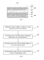
- FIG. 2 is a flowchart of a method of manufacturing a touch display device in accordance with embodiments of the present disclosure.
- a touch display device 100 in accordance with the embodiment comprises a touch panel 110, a display module 120 and a first adhesive layer 130 which laminates the touch panel 110 and the display module 120.
- the first liquid adhesive layer 130 can be formed by curing one or more of an ultraviolet-curing liquid adhesive, a heat-induced ultraviolet-curing liquid adhesive, or a moisture-induced ultraviolet-curing liquid adhesive.
- an ultraviolet-curing liquid adhesive is used.
- the ultraviolet-curing liquid adhesive is a liquid adhesive which can be cured into a solid state under irradiation of ultraviolet light of a proper wavelength, wherein the liquid adhesive could either be an acrylic or a silicon-based product.
- the touch panel 110 comprises a touch substrate 112, a lens 114, and a second adhesive layer 118, which laminates the touch substrate 112 and the lens 114.
- a shading area (not shown in FIG. 1 ) is formed by covering printing ink around the lens 114, and a touch sensing layer (not shown in FIG. 1 ) is formed on the surface of the touch substrate 112.
- the touch panel 110 further comprises of a flexible circuit board 116 which is laminated on to the touch substrate 112.
- a surrounding circuit layer (not shown in FIG. 1 ) can further be disposed on the touch substrate 112.
- the touch sensing layer is electrically connected to the surrounding circuit layer, and the surrounding circuit layer is electrically connected to the flexible circuit board 116.
- the lens 114 can be made of a glass, plastic or any other material and disposed to protect the touch display device 100 and improve strength of the touch display device 100.
- the touch substrate 112 is an element disposed to realize the touch technology and can be made of a transparent ITO (Indium Tin Oxide) glass or a film which is processed by a thin-film technology.
- the touch substrate 112 can be a resistive touch substrate or a capacitive touch substrate.
- the flexible circuit board 116 is a bridge connecting the touch substrate layer 112 and the touch system, wherein the flexible circuit board 116 usually comprises of an IC (integrated circuit) and other elements, which can compute collected touch information.
- the second adhesive layer 118 can be formed by curing of one or more of an ultraviolet-curing liquid adhesive, a heat-induced ultraviolet-curing liquid adhesive, or a moisture-induced ultraviolet-curing liquid adhesive.
- an ultraviolet-curing liquid adhesive e.g., a heat-induced ultraviolet-curing liquid adhesive, or a moisture-induced ultraviolet-curing liquid adhesive.
- the heat-induced ultraviolet-curing liquid adhesive or the moisture-induced ultraviolet-curing liquid adhesive is used.
- the heat-induced ultraviolet-curing liquid adhesive is a liquid adhesive which can be cured into a solid state under irradiation of an ultraviolet light of a proper wavelength, and the area that is not irradiated by the ultraviolet light can then be cured by heat.
- the moisture-induced ultraviolet-curing liquid adhesive is a liquid adhesive which can be cured into a solid state under the irradiation of an ultraviolet light of a proper wavelength, and the area that is not irradiated by the ultraviolet light can then be cured by moisture.
- the heat-induced ultraviolet-curing liquid adhesive or the moisture-induced ultraviolet-curing liquid adhesive can either be acryl-based or silicon-based product.
- the display module 120 comprises of a display panel 122 and at least one diffuser 124 which is laminated to the display 122.
- the first adhesive layer 130 is disposed between the diffuser 124 and the touch substrate 112.
- the display 122 could be any of liquid crystal display (LCD), organic light-emitting diode display (OLED), interferometric modulator display (IMOD), cathode ray tube display, plasma display or E-paper display.
- FIG. 2 shows a flowchart for a method of manufacturing a touch display device 100 in accordance with the present embodiments, wherein the method comprises the steps of:
- the first liquid adhesive and the second liquid adhesive are light-curing liquid adhesives including but not limited to ultraviolet-curing liquid adhesive, heat-induced ultraviolet-curing liquid adhesive, or moisture-induced ultraviolet-curing liquid adhesive.
- the method of light curing comprises:
- the method of light curing comprises:
- a flexible circuit board 116 can be laminated to the touch substrate 112 first and then the touch substrate 112 along with the flexible circuit board 116 can be laminated to the display module 120.
- the touch panel and the display module are laminated by a conventional method, ultraviolet light is unable to pass through the shading layer formed by printing ink on the lens, leading to incomplete light curing of the light-curing liquid adhesive under the printing ink of the lens.
- An advantage of using the present method is that the touch substrate layer and the flexible circuit board are substantially transparent, such that the ultraviolet-curing liquid adhesive can be completely light-cured to form an adhesive layer through ultraviolet irradiation. Moreover, there is no influence of printing ink on the lens, and therefore the ultraviolet-curing liquid adhesive is completely light-cured.
Landscapes
- Engineering & Computer Science (AREA)
- Theoretical Computer Science (AREA)
- General Engineering & Computer Science (AREA)
- Physics & Mathematics (AREA)
- General Physics & Mathematics (AREA)
- Human Computer Interaction (AREA)
- Microelectronics & Electronic Packaging (AREA)
- Position Input By Displaying (AREA)
- Devices For Indicating Variable Information By Combining Individual Elements (AREA)
- Adhesives Or Adhesive Processes (AREA)
- Lining Or Joining Of Plastics Or The Like (AREA)
Applications Claiming Priority (1)
| Application Number | Priority Date | Filing Date | Title |
|---|---|---|---|
| CN2011102895722A CN102999200A (zh) | 2011-09-18 | 2011-09-18 | 触控显示装置及其制造方法 |
Publications (3)
| Publication Number | Publication Date |
|---|---|
| EP2570899A2 true EP2570899A2 (fr) | 2013-03-20 |
| EP2570899A3 EP2570899A3 (fr) | 2015-06-10 |
| EP2570899B1 EP2570899B1 (fr) | 2017-11-08 |
Family
ID=47178456
Family Applications (1)
| Application Number | Title | Priority Date | Filing Date |
|---|---|---|---|
| EP12183962.5A Not-in-force EP2570899B1 (fr) | 2011-09-18 | 2012-09-12 | Dispositif d'écran tactile et son procédé de fabrication |
Country Status (6)
| Country | Link |
|---|---|
| US (1) | US20130069890A1 (fr) |
| EP (1) | EP2570899B1 (fr) |
| JP (1) | JP5686777B2 (fr) |
| KR (1) | KR101452954B1 (fr) |
| CN (1) | CN102999200A (fr) |
| TW (2) | TWI581133B (fr) |
Cited By (5)
| Publication number | Priority date | Publication date | Assignee | Title |
|---|---|---|---|---|
| US11987731B2 (en) | 2018-08-10 | 2024-05-21 | Dow Toray Co., Ltd. | Organopolysiloxane composition for forming pressure sensitive adhesive layer, and use of same |
| US12173197B2 (en) | 2018-08-10 | 2024-12-24 | Dow Toray Co., Ltd. | Organopolysiloxane composition for forming pressure sensitive adhesive layer, and use of same |
| US12503630B2 (en) | 2019-08-13 | 2025-12-23 | Dow Toray Co., Ltd. | Organopolysiloxane composition having pressure-sensitive adhesive layer formation properties, and use of said composition |
| US12503626B2 (en) | 2019-08-13 | 2025-12-23 | Dow Toray Co., Ltd. | Organopolysiloxane composition for forming pressure sensitive adhesive layer and use of same |
| US12509614B2 (en) | 2018-08-10 | 2025-12-30 | Dow Toray Co., Ltd. | Organopolysiloxane composition for forming pressure sensitive adhesive layer, and use of same |
Families Citing this family (22)
| Publication number | Priority date | Publication date | Assignee | Title |
|---|---|---|---|---|
| US20150062448A1 (en) * | 2013-08-30 | 2015-03-05 | Arvind S. | Touch screen displays |
| JP6378184B2 (ja) * | 2013-09-09 | 2018-08-22 | 日本化薬株式会社 | 光学部材の製造方法及びそれに用いる紫外線硬化型樹脂組成物 |
| TW201512915A (zh) * | 2013-09-18 | 2015-04-01 | Silitech Technology Corp | 觸控面板 |
| CN104635963B (zh) * | 2013-11-07 | 2018-02-23 | 群创光电股份有限公司 | 触控显示装置与其制造方法 |
| US20160329562A1 (en) | 2014-12-16 | 2016-11-10 | Sanyo Electric Co., Ltd. | Negative electrode active material for nonaqueous electrolyte secondary batteries and nonaqueous electrolyte secondary battery containing negative electrode active material |
| EP3281984B1 (fr) | 2015-04-10 | 2024-01-31 | Dow Toray Co., Ltd. | Composition d'organopolysiloxane durcissable comprenant un groupe fluoroalkyle, article durci associé, et composant électronique ou dispositif d'affichage équipé de cet article durci |
| CN105204686B (zh) * | 2015-09-23 | 2019-05-31 | 联想(北京)有限公司 | 一种电子设备 |
| US20170108959A1 (en) * | 2015-10-15 | 2017-04-20 | Richard Keith McMillan | Two piece lens assembly |
| CN105468199B (zh) * | 2015-12-26 | 2019-01-15 | 宸鸿科技(厦门)有限公司 | 一种具有压力感测的面板 |
| EP3447082A4 (fr) | 2016-04-22 | 2019-11-27 | Dow Toray Co., Ltd. | Film hautement diélectrique, ses utilisations et son procédé de fabrication |
| CN106873827B (zh) * | 2017-01-16 | 2020-04-17 | 业成科技(成都)有限公司 | 触控偏光单元、可挠性触控显示设备以及可挠性触控显示设备的制造方法 |
| EP3608383A4 (fr) | 2017-04-03 | 2020-12-30 | Dow Toray Co., Ltd. | Résine d'organopolysiloxane réactive au durcissement, composition adhésive sensible à la pression utilisant celle-ci et utilisation de celle-ci |
| KR102515709B1 (ko) | 2017-07-07 | 2023-04-03 | 다우 도레이 캄파니 리미티드 | 감압접착층 형성용 오가노폴리실록산 조성물 및 그 사용 |
| JP7419251B2 (ja) | 2018-10-30 | 2024-01-22 | ダウ・東レ株式会社 | 硬化反応性シリコーン組成物及びその硬化物並びにそれらの用途 |
| EP3896137B1 (fr) | 2018-12-13 | 2025-11-12 | Dow Toray Co., Ltd. | Composition adhésive à base de silicones et son utilisation |
| CN110413154A (zh) * | 2019-07-25 | 2019-11-05 | 深圳市华星光电半导体显示技术有限公司 | 触控显示装置及其制造方法 |
| JP7648329B2 (ja) | 2019-08-13 | 2025-03-18 | ダウ・東レ株式会社 | 感圧接着層形成性オルガノポリシロキサン組成物およびその使用 |
| CN113359339A (zh) * | 2020-03-06 | 2021-09-07 | 北京小米移动软件有限公司 | 显示屏、显示屏防水处理工艺和终端设备 |
| CN111524939A (zh) * | 2020-04-26 | 2020-08-11 | 武汉华星光电半导体显示技术有限公司 | 柔性显示面板及其组装方法 |
| KR20220072927A (ko) * | 2020-11-25 | 2022-06-03 | 삼성디스플레이 주식회사 | 표시 장치 및 그 제조 방법 |
| KR20230125248A (ko) | 2020-12-25 | 2023-08-29 | 다우 도레이 캄파니 리미티드 | 실리콘 점착제 조성물 및 그의 용도 |
| TWI767665B (zh) * | 2021-04-22 | 2022-06-11 | 群光電子股份有限公司 | 觸控板裝置及其製造方法 |
Family Cites Families (17)
| Publication number | Priority date | Publication date | Assignee | Title |
|---|---|---|---|---|
| JP2005107655A (ja) * | 2003-09-29 | 2005-04-21 | Kawaguchiko Seimitsu Co Ltd | タッチパネル及びその製造方法 |
| JP2006235571A (ja) * | 2005-01-28 | 2006-09-07 | Victor Co Of Japan Ltd | 投射型表示装置 |
| JP5413937B2 (ja) * | 2006-09-28 | 2014-02-12 | 株式会社ジャパンディスプレイ | 電気光学装置及び電子機器 |
| JP2009163132A (ja) * | 2008-01-09 | 2009-07-23 | Seiko Instruments Inc | 液晶表示装置の製造方法、液晶表示装置、及び電子機器 |
| JP5243811B2 (ja) * | 2008-02-14 | 2013-07-24 | セイコーインスツル株式会社 | 表示装置 |
| CN201174007Y (zh) * | 2008-03-18 | 2008-12-31 | 宸鸿光电科技股份有限公司 | 电容式触控面板 |
| US9573346B2 (en) * | 2008-05-21 | 2017-02-21 | Manufacturing Resources International, Inc. | Photoinitiated optical adhesive and method for using same |
| JP5451036B2 (ja) * | 2008-11-21 | 2014-03-26 | 株式会社ジャパンディスプレイ | 表示装置及びその製造方法 |
| JP2010197692A (ja) * | 2009-02-25 | 2010-09-09 | Sekisui Chem Co Ltd | 光学部材用光硬化性樹脂組成物、接着剤、及び、タッチパネル |
| JP5235769B2 (ja) * | 2009-04-27 | 2013-07-10 | 株式会社ジャパンディスプレイイースト | 液晶表示装置 |
| TWI412817B (zh) * | 2009-06-02 | 2013-10-21 | Wintek Corp | 觸控顯示裝置 |
| US20110005662A1 (en) * | 2009-07-10 | 2011-01-13 | Kuo-Hua Sung | Method for Fabricating Multilayer Panels |
| KR101229419B1 (ko) * | 2009-11-12 | 2013-02-05 | (주)멜파스 | 이방 전도성 접착제를 포함하는 접촉 감지 패널 및 그 제조 방법 |
| TW201102698A (en) * | 2010-01-26 | 2011-01-16 | Mastouch Optoelectronics Technologies Co Ltd | Single-layer projected capacitive touch panel and fabricating method thereof |
| WO2011112447A2 (fr) * | 2010-03-09 | 2011-09-15 | 3M Innovative Properties Company | Adhésif optiquement transparent thermocollant destiné à l'assemblage de panneaux d'affichage |
| CN101973155B (zh) * | 2010-08-24 | 2013-04-10 | 深圳市中显微电子有限公司 | 电容式触摸屏基板贴合方法以及触摸屏与显示模块的贴合方法 |
| CN202422050U (zh) * | 2011-09-18 | 2012-09-05 | 宸鸿科技(厦门)有限公司 | 触控显示装置 |
-
2011
- 2011-09-18 CN CN2011102895722A patent/CN102999200A/zh active Pending
-
2012
- 2012-04-03 TW TW101111765A patent/TWI581133B/zh not_active IP Right Cessation
- 2012-04-03 TW TW101206004U patent/TWM440475U/zh not_active IP Right Cessation
- 2012-07-26 US US13/559,532 patent/US20130069890A1/en not_active Abandoned
- 2012-08-30 KR KR1020120095756A patent/KR101452954B1/ko not_active Expired - Fee Related
- 2012-09-03 JP JP2012192809A patent/JP5686777B2/ja not_active Expired - Fee Related
- 2012-09-12 EP EP12183962.5A patent/EP2570899B1/fr not_active Not-in-force
Non-Patent Citations (1)
| Title |
|---|
| None |
Cited By (5)
| Publication number | Priority date | Publication date | Assignee | Title |
|---|---|---|---|---|
| US11987731B2 (en) | 2018-08-10 | 2024-05-21 | Dow Toray Co., Ltd. | Organopolysiloxane composition for forming pressure sensitive adhesive layer, and use of same |
| US12173197B2 (en) | 2018-08-10 | 2024-12-24 | Dow Toray Co., Ltd. | Organopolysiloxane composition for forming pressure sensitive adhesive layer, and use of same |
| US12509614B2 (en) | 2018-08-10 | 2025-12-30 | Dow Toray Co., Ltd. | Organopolysiloxane composition for forming pressure sensitive adhesive layer, and use of same |
| US12503630B2 (en) | 2019-08-13 | 2025-12-23 | Dow Toray Co., Ltd. | Organopolysiloxane composition having pressure-sensitive adhesive layer formation properties, and use of said composition |
| US12503626B2 (en) | 2019-08-13 | 2025-12-23 | Dow Toray Co., Ltd. | Organopolysiloxane composition for forming pressure sensitive adhesive layer and use of same |
Also Published As
| Publication number | Publication date |
|---|---|
| KR101452954B1 (ko) | 2014-10-21 |
| EP2570899A3 (fr) | 2015-06-10 |
| TWI581133B (zh) | 2017-05-01 |
| JP5686777B2 (ja) | 2015-03-18 |
| TW201314522A (zh) | 2013-04-01 |
| TWM440475U (en) | 2012-11-01 |
| KR20130030721A (ko) | 2013-03-27 |
| JP2013065009A (ja) | 2013-04-11 |
| EP2570899B1 (fr) | 2017-11-08 |
| US20130069890A1 (en) | 2013-03-21 |
| CN102999200A (zh) | 2013-03-27 |
Similar Documents
| Publication | Publication Date | Title |
|---|---|---|
| EP2570899A2 (fr) | Dispositif d'écran tactile et son procédé de fabrication | |
| CN108417145B (zh) | 一种显示器全贴合工艺 | |
| CN109752874B (zh) | 面板模块及显示装置 | |
| TW201303431A (zh) | 觸控面板一體型顯示裝置及其製造方法 | |
| CN103151467A (zh) | 集成有触摸屏的有机发光显示装置及其制造方法 | |
| KR20160061903A (ko) | 어레이 기판 및 그 제조 방법, 유연 디스플레이 패널 및 디스플레이 디바이스 | |
| CN102844802B (zh) | 显示装置的制造方法 | |
| US9375897B2 (en) | Display device and method for producing the same | |
| US10338708B2 (en) | Flexible touch screen, method for manufacturing the same and touch device | |
| WO2014123165A1 (fr) | Matériau de surface transparente et dispositif d'affichage utilisant celui-ci | |
| CN103676271A (zh) | 显示装置以及罩部件 | |
| JP2014013266A (ja) | 表示装置及びその製造方法 | |
| JP2014157311A (ja) | 表示装置および表示装置の製造方法 | |
| WO2021068395A1 (fr) | Dispositif d'affichage tactile et procédé de fabrication correspondant | |
| US20150239211A1 (en) | Laminate comprising adhesive layer and method for manufacturing same | |
| TWI566005B (zh) | 製作顯示面板之方法 | |
| KR20210083546A (ko) | 유기 발광 표시 장치 및 유기 발광 표시 장치 제조 방법 | |
| KR20200012068A (ko) | 표시 장치 및 이의 제조 방법 | |
| CN202422050U (zh) | 触控显示装置 | |
| CN204382745U (zh) | 超薄触控显示屏 | |
| KR20110119347A (ko) | 편광필름을 이용한 정전용량 터치 패널 구현을 통한 액정표시모듈과의 일체화 | |
| CN201159888Y (zh) | 全平面触控面板 | |
| KR102845994B1 (ko) | 표시 장치 | |
| WO2013161868A1 (fr) | Dispositif d'affichage équipé d'un panneau tactile | |
| KR102026111B1 (ko) | 터치패널 및 그 제조 방법 |
Legal Events
| Date | Code | Title | Description |
|---|---|---|---|
| PUAI | Public reference made under article 153(3) epc to a published international application that has entered the european phase |
Free format text: ORIGINAL CODE: 0009012 |
|
| AK | Designated contracting states |
Kind code of ref document: A2 Designated state(s): AL AT BE BG CH CY CZ DE DK EE ES FI FR GB GR HR HU IE IS IT LI LT LU LV MC MK MT NL NO PL PT RO RS SE SI SK SM TR |
|
| AX | Request for extension of the european patent |
Extension state: BA ME |
|
| PUAL | Search report despatched |
Free format text: ORIGINAL CODE: 0009013 |
|
| AK | Designated contracting states |
Kind code of ref document: A3 Designated state(s): AL AT BE BG CH CY CZ DE DK EE ES FI FR GB GR HR HU IE IS IT LI LT LU LV MC MK MT NL NO PL PT RO RS SE SI SK SM TR |
|
| AX | Request for extension of the european patent |
Extension state: BA ME |
|
| RIC1 | Information provided on ipc code assigned before grant |
Ipc: B32B 7/12 20060101ALI20150506BHEP Ipc: G06F 3/041 20060101AFI20150506BHEP |
|
| 17P | Request for examination filed |
Effective date: 20151208 |
|
| RBV | Designated contracting states (corrected) |
Designated state(s): AL AT BE BG CH CY CZ DE DK EE ES FI FR GB GR HR HU IE IS IT LI LT LU LV MC MK MT NL NO PL PT RO RS SE SI SK SM TR |
|
| 17Q | First examination report despatched |
Effective date: 20160223 |
|
| GRAP | Despatch of communication of intention to grant a patent |
Free format text: ORIGINAL CODE: EPIDOSNIGR1 |
|
| STAA | Information on the status of an ep patent application or granted ep patent |
Free format text: STATUS: GRANT OF PATENT IS INTENDED |
|
| INTG | Intention to grant announced |
Effective date: 20170720 |
|
| GRAS | Grant fee paid |
Free format text: ORIGINAL CODE: EPIDOSNIGR3 |
|
| GRAA | (expected) grant |
Free format text: ORIGINAL CODE: 0009210 |
|
| STAA | Information on the status of an ep patent application or granted ep patent |
Free format text: STATUS: THE PATENT HAS BEEN GRANTED |
|
| AK | Designated contracting states |
Kind code of ref document: B1 Designated state(s): AL AT BE BG CH CY CZ DE DK EE ES FI FR GB GR HR HU IE IS IT LI LT LU LV MC MK MT NL NO PL PT RO RS SE SI SK SM TR |
|
| REG | Reference to a national code |
Ref country code: GB Ref legal event code: FG4D |
|
| REG | Reference to a national code |
Ref country code: CH Ref legal event code: EP Ref country code: AT Ref legal event code: REF Ref document number: 944757 Country of ref document: AT Kind code of ref document: T Effective date: 20171115 |
|
| REG | Reference to a national code |
Ref country code: IE Ref legal event code: FG4D |
|
| REG | Reference to a national code |
Ref country code: DE Ref legal event code: R096 Ref document number: 602012039427 Country of ref document: DE |
|
| REG | Reference to a national code |
Ref country code: NL Ref legal event code: MP Effective date: 20171108 |
|
| REG | Reference to a national code |
Ref country code: LT Ref legal event code: MG4D |
|
| REG | Reference to a national code |
Ref country code: AT Ref legal event code: MK05 Ref document number: 944757 Country of ref document: AT Kind code of ref document: T Effective date: 20171108 |
|
| PG25 | Lapsed in a contracting state [announced via postgrant information from national office to epo] |
Ref country code: SE Free format text: LAPSE BECAUSE OF FAILURE TO SUBMIT A TRANSLATION OF THE DESCRIPTION OR TO PAY THE FEE WITHIN THE PRESCRIBED TIME-LIMIT Effective date: 20171108 Ref country code: NL Free format text: LAPSE BECAUSE OF FAILURE TO SUBMIT A TRANSLATION OF THE DESCRIPTION OR TO PAY THE FEE WITHIN THE PRESCRIBED TIME-LIMIT Effective date: 20171108 Ref country code: FI Free format text: LAPSE BECAUSE OF FAILURE TO SUBMIT A TRANSLATION OF THE DESCRIPTION OR TO PAY THE FEE WITHIN THE PRESCRIBED TIME-LIMIT Effective date: 20171108 Ref country code: LT Free format text: LAPSE BECAUSE OF FAILURE TO SUBMIT A TRANSLATION OF THE DESCRIPTION OR TO PAY THE FEE WITHIN THE PRESCRIBED TIME-LIMIT Effective date: 20171108 Ref country code: ES Free format text: LAPSE BECAUSE OF FAILURE TO SUBMIT A TRANSLATION OF THE DESCRIPTION OR TO PAY THE FEE WITHIN THE PRESCRIBED TIME-LIMIT Effective date: 20171108 Ref country code: NO Free format text: LAPSE BECAUSE OF FAILURE TO SUBMIT A TRANSLATION OF THE DESCRIPTION OR TO PAY THE FEE WITHIN THE PRESCRIBED TIME-LIMIT Effective date: 20180208 |
|
| PG25 | Lapsed in a contracting state [announced via postgrant information from national office to epo] |
Ref country code: BG Free format text: LAPSE BECAUSE OF FAILURE TO SUBMIT A TRANSLATION OF THE DESCRIPTION OR TO PAY THE FEE WITHIN THE PRESCRIBED TIME-LIMIT Effective date: 20180208 Ref country code: LV Free format text: LAPSE BECAUSE OF FAILURE TO SUBMIT A TRANSLATION OF THE DESCRIPTION OR TO PAY THE FEE WITHIN THE PRESCRIBED TIME-LIMIT Effective date: 20171108 Ref country code: GR Free format text: LAPSE BECAUSE OF FAILURE TO SUBMIT A TRANSLATION OF THE DESCRIPTION OR TO PAY THE FEE WITHIN THE PRESCRIBED TIME-LIMIT Effective date: 20180209 Ref country code: IS Free format text: LAPSE BECAUSE OF FAILURE TO SUBMIT A TRANSLATION OF THE DESCRIPTION OR TO PAY THE FEE WITHIN THE PRESCRIBED TIME-LIMIT Effective date: 20180308 Ref country code: RS Free format text: LAPSE BECAUSE OF FAILURE TO SUBMIT A TRANSLATION OF THE DESCRIPTION OR TO PAY THE FEE WITHIN THE PRESCRIBED TIME-LIMIT Effective date: 20171108 Ref country code: HR Free format text: LAPSE BECAUSE OF FAILURE TO SUBMIT A TRANSLATION OF THE DESCRIPTION OR TO PAY THE FEE WITHIN THE PRESCRIBED TIME-LIMIT Effective date: 20171108 Ref country code: AT Free format text: LAPSE BECAUSE OF FAILURE TO SUBMIT A TRANSLATION OF THE DESCRIPTION OR TO PAY THE FEE WITHIN THE PRESCRIBED TIME-LIMIT Effective date: 20171108 |
|
| PG25 | Lapsed in a contracting state [announced via postgrant information from national office to epo] |
Ref country code: CZ Free format text: LAPSE BECAUSE OF FAILURE TO SUBMIT A TRANSLATION OF THE DESCRIPTION OR TO PAY THE FEE WITHIN THE PRESCRIBED TIME-LIMIT Effective date: 20171108 Ref country code: EE Free format text: LAPSE BECAUSE OF FAILURE TO SUBMIT A TRANSLATION OF THE DESCRIPTION OR TO PAY THE FEE WITHIN THE PRESCRIBED TIME-LIMIT Effective date: 20171108 Ref country code: CY Free format text: LAPSE BECAUSE OF FAILURE TO SUBMIT A TRANSLATION OF THE DESCRIPTION OR TO PAY THE FEE WITHIN THE PRESCRIBED TIME-LIMIT Effective date: 20171108 Ref country code: DK Free format text: LAPSE BECAUSE OF FAILURE TO SUBMIT A TRANSLATION OF THE DESCRIPTION OR TO PAY THE FEE WITHIN THE PRESCRIBED TIME-LIMIT Effective date: 20171108 Ref country code: SK Free format text: LAPSE BECAUSE OF FAILURE TO SUBMIT A TRANSLATION OF THE DESCRIPTION OR TO PAY THE FEE WITHIN THE PRESCRIBED TIME-LIMIT Effective date: 20171108 |
|
| REG | Reference to a national code |
Ref country code: DE Ref legal event code: R097 Ref document number: 602012039427 Country of ref document: DE |
|
| PG25 | Lapsed in a contracting state [announced via postgrant information from national office to epo] |
Ref country code: IT Free format text: LAPSE BECAUSE OF FAILURE TO SUBMIT A TRANSLATION OF THE DESCRIPTION OR TO PAY THE FEE WITHIN THE PRESCRIBED TIME-LIMIT Effective date: 20171108 Ref country code: SM Free format text: LAPSE BECAUSE OF FAILURE TO SUBMIT A TRANSLATION OF THE DESCRIPTION OR TO PAY THE FEE WITHIN THE PRESCRIBED TIME-LIMIT Effective date: 20171108 Ref country code: RO Free format text: LAPSE BECAUSE OF FAILURE TO SUBMIT A TRANSLATION OF THE DESCRIPTION OR TO PAY THE FEE WITHIN THE PRESCRIBED TIME-LIMIT Effective date: 20171108 Ref country code: PL Free format text: LAPSE BECAUSE OF FAILURE TO SUBMIT A TRANSLATION OF THE DESCRIPTION OR TO PAY THE FEE WITHIN THE PRESCRIBED TIME-LIMIT Effective date: 20171108 |
|
| PLBE | No opposition filed within time limit |
Free format text: ORIGINAL CODE: 0009261 |
|
| STAA | Information on the status of an ep patent application or granted ep patent |
Free format text: STATUS: NO OPPOSITION FILED WITHIN TIME LIMIT |
|
| 26N | No opposition filed |
Effective date: 20180809 |
|
| PG25 | Lapsed in a contracting state [announced via postgrant information from national office to epo] |
Ref country code: SI Free format text: LAPSE BECAUSE OF FAILURE TO SUBMIT A TRANSLATION OF THE DESCRIPTION OR TO PAY THE FEE WITHIN THE PRESCRIBED TIME-LIMIT Effective date: 20171108 |
|
| REG | Reference to a national code |
Ref country code: DE Ref legal event code: R119 Ref document number: 602012039427 Country of ref document: DE |
|
| PG25 | Lapsed in a contracting state [announced via postgrant information from national office to epo] |
Ref country code: MC Free format text: LAPSE BECAUSE OF FAILURE TO SUBMIT A TRANSLATION OF THE DESCRIPTION OR TO PAY THE FEE WITHIN THE PRESCRIBED TIME-LIMIT Effective date: 20171108 |
|
| REG | Reference to a national code |
Ref country code: CH Ref legal event code: PL |
|
| GBPC | Gb: european patent ceased through non-payment of renewal fee |
Effective date: 20180912 |
|
| REG | Reference to a national code |
Ref country code: BE Ref legal event code: MM Effective date: 20180930 |
|
| REG | Reference to a national code |
Ref country code: IE Ref legal event code: MM4A |
|
| PG25 | Lapsed in a contracting state [announced via postgrant information from national office to epo] |
Ref country code: LU Free format text: LAPSE BECAUSE OF NON-PAYMENT OF DUE FEES Effective date: 20180912 |
|
| PG25 | Lapsed in a contracting state [announced via postgrant information from national office to epo] |
Ref country code: IE Free format text: LAPSE BECAUSE OF NON-PAYMENT OF DUE FEES Effective date: 20180912 Ref country code: DE Free format text: LAPSE BECAUSE OF NON-PAYMENT OF DUE FEES Effective date: 20190402 |
|
| PG25 | Lapsed in a contracting state [announced via postgrant information from national office to epo] |
Ref country code: BE Free format text: LAPSE BECAUSE OF NON-PAYMENT OF DUE FEES Effective date: 20180930 Ref country code: FR Free format text: LAPSE BECAUSE OF NON-PAYMENT OF DUE FEES Effective date: 20180930 Ref country code: LI Free format text: LAPSE BECAUSE OF NON-PAYMENT OF DUE FEES Effective date: 20180930 Ref country code: CH Free format text: LAPSE BECAUSE OF NON-PAYMENT OF DUE FEES Effective date: 20180930 |
|
| PG25 | Lapsed in a contracting state [announced via postgrant information from national office to epo] |
Ref country code: GB Free format text: LAPSE BECAUSE OF NON-PAYMENT OF DUE FEES Effective date: 20180912 |
|
| PG25 | Lapsed in a contracting state [announced via postgrant information from national office to epo] |
Ref country code: MT Free format text: LAPSE BECAUSE OF NON-PAYMENT OF DUE FEES Effective date: 20180912 |
|
| PG25 | Lapsed in a contracting state [announced via postgrant information from national office to epo] |
Ref country code: TR Free format text: LAPSE BECAUSE OF FAILURE TO SUBMIT A TRANSLATION OF THE DESCRIPTION OR TO PAY THE FEE WITHIN THE PRESCRIBED TIME-LIMIT Effective date: 20171108 |
|
| PG25 | Lapsed in a contracting state [announced via postgrant information from national office to epo] |
Ref country code: HU Free format text: LAPSE BECAUSE OF FAILURE TO SUBMIT A TRANSLATION OF THE DESCRIPTION OR TO PAY THE FEE WITHIN THE PRESCRIBED TIME-LIMIT; INVALID AB INITIO Effective date: 20120912 Ref country code: PT Free format text: LAPSE BECAUSE OF FAILURE TO SUBMIT A TRANSLATION OF THE DESCRIPTION OR TO PAY THE FEE WITHIN THE PRESCRIBED TIME-LIMIT Effective date: 20171108 |
|
| PG25 | Lapsed in a contracting state [announced via postgrant information from national office to epo] |
Ref country code: MK Free format text: LAPSE BECAUSE OF NON-PAYMENT OF DUE FEES Effective date: 20171108 |
|
| PG25 | Lapsed in a contracting state [announced via postgrant information from national office to epo] |
Ref country code: AL Free format text: LAPSE BECAUSE OF FAILURE TO SUBMIT A TRANSLATION OF THE DESCRIPTION OR TO PAY THE FEE WITHIN THE PRESCRIBED TIME-LIMIT Effective date: 20171108 |