EP2573810B1 - Halbleiterbauelement - Google Patents
Halbleiterbauelement Download PDFInfo
- Publication number
- EP2573810B1 EP2573810B1 EP10851766.5A EP10851766A EP2573810B1 EP 2573810 B1 EP2573810 B1 EP 2573810B1 EP 10851766 A EP10851766 A EP 10851766A EP 2573810 B1 EP2573810 B1 EP 2573810B1
- Authority
- EP
- European Patent Office
- Prior art keywords
- electrode
- semiconductor device
- resin
- substrate
- semiconductor element
- Prior art date
- Legal status (The legal status is an assumption and is not a legal conclusion. Google has not performed a legal analysis and makes no representation as to the accuracy of the status listed.)
- Not-in-force
Links
Images
Classifications
-
- H—ELECTRICITY
- H10—SEMICONDUCTOR DEVICES; ELECTRIC SOLID-STATE DEVICES NOT OTHERWISE PROVIDED FOR
- H10W—GENERIC PACKAGES, INTERCONNECTIONS, CONNECTORS OR OTHER CONSTRUCTIONAL DETAILS OF DEVICES COVERED BY CLASS H10
- H10W74/00—Encapsulations, e.g. protective coatings
- H10W74/01—Manufacture or treatment
-
- C—CHEMISTRY; METALLURGY
- C23—COATING METALLIC MATERIAL; COATING MATERIAL WITH METALLIC MATERIAL; CHEMICAL SURFACE TREATMENT; DIFFUSION TREATMENT OF METALLIC MATERIAL; COATING BY VACUUM EVAPORATION, BY SPUTTERING, BY ION IMPLANTATION OR BY CHEMICAL VAPOUR DEPOSITION, IN GENERAL; INHIBITING CORROSION OF METALLIC MATERIAL OR INCRUSTATION IN GENERAL
- C23C—COATING METALLIC MATERIAL; COATING MATERIAL WITH METALLIC MATERIAL; SURFACE TREATMENT OF METALLIC MATERIAL BY DIFFUSION INTO THE SURFACE, BY CHEMICAL CONVERSION OR SUBSTITUTION; COATING BY VACUUM EVAPORATION, BY SPUTTERING, BY ION IMPLANTATION OR BY CHEMICAL VAPOUR DEPOSITION, IN GENERAL
- C23C24/00—Coating starting from inorganic powder
- C23C24/02—Coating starting from inorganic powder by application of pressure only
- C23C24/04—Impact or kinetic deposition of particles
-
- C—CHEMISTRY; METALLURGY
- C23—COATING METALLIC MATERIAL; COATING MATERIAL WITH METALLIC MATERIAL; CHEMICAL SURFACE TREATMENT; DIFFUSION TREATMENT OF METALLIC MATERIAL; COATING BY VACUUM EVAPORATION, BY SPUTTERING, BY ION IMPLANTATION OR BY CHEMICAL VAPOUR DEPOSITION, IN GENERAL; INHIBITING CORROSION OF METALLIC MATERIAL OR INCRUSTATION IN GENERAL
- C23C—COATING METALLIC MATERIAL; COATING MATERIAL WITH METALLIC MATERIAL; SURFACE TREATMENT OF METALLIC MATERIAL BY DIFFUSION INTO THE SURFACE, BY CHEMICAL CONVERSION OR SUBSTITUTION; COATING BY VACUUM EVAPORATION, BY SPUTTERING, BY ION IMPLANTATION OR BY CHEMICAL VAPOUR DEPOSITION, IN GENERAL
- C23C28/00—Coating for obtaining at least two superposed coatings either by methods not provided for in a single one of groups C23C2/00 - C23C26/00 or by combinations of methods provided for in subclasses C23C and C25C or C25D
-
- H—ELECTRICITY
- H10—SEMICONDUCTOR DEVICES; ELECTRIC SOLID-STATE DEVICES NOT OTHERWISE PROVIDED FOR
- H10W—GENERIC PACKAGES, INTERCONNECTIONS, CONNECTORS OR OTHER CONSTRUCTIONAL DETAILS OF DEVICES COVERED BY CLASS H10
- H10W40/00—Arrangements for thermal protection or thermal control
- H10W40/70—Fillings or auxiliary members in containers or in encapsulations for thermal protection or control
- H10W40/77—Auxiliary members characterised by their shape
- H10W40/778—Auxiliary members characterised by their shape in encapsulations
-
- H—ELECTRICITY
- H10—SEMICONDUCTOR DEVICES; ELECTRIC SOLID-STATE DEVICES NOT OTHERWISE PROVIDED FOR
- H10W—GENERIC PACKAGES, INTERCONNECTIONS, CONNECTORS OR OTHER CONSTRUCTIONAL DETAILS OF DEVICES COVERED BY CLASS H10
- H10W70/00—Package substrates; Interposers; Redistribution layers [RDL]
- H10W70/40—Leadframes
- H10W70/456—Materials
- H10W70/457—Materials of metallic layers on leadframes
-
- H—ELECTRICITY
- H10—SEMICONDUCTOR DEVICES; ELECTRIC SOLID-STATE DEVICES NOT OTHERWISE PROVIDED FOR
- H10W—GENERIC PACKAGES, INTERCONNECTIONS, CONNECTORS OR OTHER CONSTRUCTIONAL DETAILS OF DEVICES COVERED BY CLASS H10
- H10W70/00—Package substrates; Interposers; Redistribution layers [RDL]
- H10W70/40—Leadframes
- H10W70/464—Additional interconnections in combination with leadframes
-
- H—ELECTRICITY
- H10—SEMICONDUCTOR DEVICES; ELECTRIC SOLID-STATE DEVICES NOT OTHERWISE PROVIDED FOR
- H10W—GENERIC PACKAGES, INTERCONNECTIONS, CONNECTORS OR OTHER CONSTRUCTIONAL DETAILS OF DEVICES COVERED BY CLASS H10
- H10W70/00—Package substrates; Interposers; Redistribution layers [RDL]
- H10W70/40—Leadframes
- H10W70/481—Leadframes for devices being provided for in groups H10D8/00 - H10D48/00
-
- H—ELECTRICITY
- H10—SEMICONDUCTOR DEVICES; ELECTRIC SOLID-STATE DEVICES NOT OTHERWISE PROVIDED FOR
- H10W—GENERIC PACKAGES, INTERCONNECTIONS, CONNECTORS OR OTHER CONSTRUCTIONAL DETAILS OF DEVICES COVERED BY CLASS H10
- H10W74/00—Encapsulations, e.g. protective coatings
- H10W74/10—Encapsulations, e.g. protective coatings characterised by their shape or disposition
- H10W74/111—Encapsulations, e.g. protective coatings characterised by their shape or disposition the semiconductor body being completely enclosed
- H10W74/127—Encapsulations, e.g. protective coatings characterised by their shape or disposition the semiconductor body being completely enclosed characterised by arrangements for sealing or adhesion
-
- H—ELECTRICITY
- H10—SEMICONDUCTOR DEVICES; ELECTRIC SOLID-STATE DEVICES NOT OTHERWISE PROVIDED FOR
- H10W—GENERIC PACKAGES, INTERCONNECTIONS, CONNECTORS OR OTHER CONSTRUCTIONAL DETAILS OF DEVICES COVERED BY CLASS H10
- H10W76/00—Containers; Fillings or auxiliary members therefor; Seals
- H10W76/10—Containers or parts thereof
- H10W76/12—Containers or parts thereof characterised by their shape
- H10W76/13—Containers comprising a conductive base serving as an interconnection
- H10W76/138—Containers comprising a conductive base serving as an interconnection having another interconnection being formed by a cover plate parallel to the conductive base, e.g. sandwich type
-
- H—ELECTRICITY
- H10—SEMICONDUCTOR DEVICES; ELECTRIC SOLID-STATE DEVICES NOT OTHERWISE PROVIDED FOR
- H10W—GENERIC PACKAGES, INTERCONNECTIONS, CONNECTORS OR OTHER CONSTRUCTIONAL DETAILS OF DEVICES COVERED BY CLASS H10
- H10W72/00—Interconnections or connectors in packages
- H10W72/071—Connecting or disconnecting
- H10W72/073—Connecting or disconnecting of die-attach connectors
- H10W72/07351—Connecting or disconnecting of die-attach connectors characterised by changes in properties of the die-attach connectors during connecting
- H10W72/07354—Connecting or disconnecting of die-attach connectors characterised by changes in properties of the die-attach connectors during connecting changes in dispositions
-
- H—ELECTRICITY
- H10—SEMICONDUCTOR DEVICES; ELECTRIC SOLID-STATE DEVICES NOT OTHERWISE PROVIDED FOR
- H10W—GENERIC PACKAGES, INTERCONNECTIONS, CONNECTORS OR OTHER CONSTRUCTIONAL DETAILS OF DEVICES COVERED BY CLASS H10
- H10W72/00—Interconnections or connectors in packages
- H10W72/30—Die-attach connectors
- H10W72/341—Dispositions of die-attach connectors, e.g. layouts
- H10W72/347—Dispositions of multiple die-attach connectors
-
- H—ELECTRICITY
- H10—SEMICONDUCTOR DEVICES; ELECTRIC SOLID-STATE DEVICES NOT OTHERWISE PROVIDED FOR
- H10W—GENERIC PACKAGES, INTERCONNECTIONS, CONNECTORS OR OTHER CONSTRUCTIONAL DETAILS OF DEVICES COVERED BY CLASS H10
- H10W72/00—Interconnections or connectors in packages
- H10W72/30—Die-attach connectors
- H10W72/351—Materials of die-attach connectors
- H10W72/352—Materials of die-attach connectors comprising metals or metalloids, e.g. solders
-
- H—ELECTRICITY
- H10—SEMICONDUCTOR DEVICES; ELECTRIC SOLID-STATE DEVICES NOT OTHERWISE PROVIDED FOR
- H10W—GENERIC PACKAGES, INTERCONNECTIONS, CONNECTORS OR OTHER CONSTRUCTIONAL DETAILS OF DEVICES COVERED BY CLASS H10
- H10W72/00—Interconnections or connectors in packages
- H10W72/30—Die-attach connectors
- H10W72/381—Auxiliary members
-
- H—ELECTRICITY
- H10—SEMICONDUCTOR DEVICES; ELECTRIC SOLID-STATE DEVICES NOT OTHERWISE PROVIDED FOR
- H10W—GENERIC PACKAGES, INTERCONNECTIONS, CONNECTORS OR OTHER CONSTRUCTIONAL DETAILS OF DEVICES COVERED BY CLASS H10
- H10W72/00—Interconnections or connectors in packages
- H10W72/851—Dispositions of multiple connectors or interconnections
- H10W72/853—On the same surface
- H10W72/865—Die-attach connectors and bond wires
-
- H—ELECTRICITY
- H10—SEMICONDUCTOR DEVICES; ELECTRIC SOLID-STATE DEVICES NOT OTHERWISE PROVIDED FOR
- H10W—GENERIC PACKAGES, INTERCONNECTIONS, CONNECTORS OR OTHER CONSTRUCTIONAL DETAILS OF DEVICES COVERED BY CLASS H10
- H10W72/00—Interconnections or connectors in packages
- H10W72/851—Dispositions of multiple connectors or interconnections
- H10W72/874—On different surfaces
- H10W72/884—Die-attach connectors and bond wires
-
- H—ELECTRICITY
- H10—SEMICONDUCTOR DEVICES; ELECTRIC SOLID-STATE DEVICES NOT OTHERWISE PROVIDED FOR
- H10W—GENERIC PACKAGES, INTERCONNECTIONS, CONNECTORS OR OTHER CONSTRUCTIONAL DETAILS OF DEVICES COVERED BY CLASS H10
- H10W74/00—Encapsulations, e.g. protective coatings
-
- H—ELECTRICITY
- H10—SEMICONDUCTOR DEVICES; ELECTRIC SOLID-STATE DEVICES NOT OTHERWISE PROVIDED FOR
- H10W—GENERIC PACKAGES, INTERCONNECTIONS, CONNECTORS OR OTHER CONSTRUCTIONAL DETAILS OF DEVICES COVERED BY CLASS H10
- H10W74/00—Encapsulations, e.g. protective coatings
- H10W74/10—Encapsulations, e.g. protective coatings characterised by their shape or disposition
- H10W74/111—Encapsulations, e.g. protective coatings characterised by their shape or disposition the semiconductor body being completely enclosed
-
- H—ELECTRICITY
- H10—SEMICONDUCTOR DEVICES; ELECTRIC SOLID-STATE DEVICES NOT OTHERWISE PROVIDED FOR
- H10W—GENERIC PACKAGES, INTERCONNECTIONS, CONNECTORS OR OTHER CONSTRUCTIONAL DETAILS OF DEVICES COVERED BY CLASS H10
- H10W90/00—Package configurations
- H10W90/701—Package configurations characterised by the relative positions of pads or connectors relative to package parts
- H10W90/731—Package configurations characterised by the relative positions of pads or connectors relative to package parts of die-attach connectors
- H10W90/736—Package configurations characterised by the relative positions of pads or connectors relative to package parts of die-attach connectors between a chip and a stacked lead frame, conducting package substrate or heat sink
-
- H—ELECTRICITY
- H10—SEMICONDUCTOR DEVICES; ELECTRIC SOLID-STATE DEVICES NOT OTHERWISE PROVIDED FOR
- H10W—GENERIC PACKAGES, INTERCONNECTIONS, CONNECTORS OR OTHER CONSTRUCTIONAL DETAILS OF DEVICES COVERED BY CLASS H10
- H10W90/00—Package configurations
- H10W90/701—Package configurations characterised by the relative positions of pads or connectors relative to package parts
- H10W90/751—Package configurations characterised by the relative positions of pads or connectors relative to package parts of bond wires
- H10W90/756—Package configurations characterised by the relative positions of pads or connectors relative to package parts of bond wires between a chip and a stacked lead frame, conducting package substrate or heat sink
Definitions
- the present invention relates to a semiconductor device provided at low cost with improved bonding strength (contact strength) between a substrate and a sealing resin.
- a semiconductor device is configured such that a semiconductor element is bonded to a substrate through solder and further this assembly is entirely sealingly covered with resin.
- the substrate however has a large coefficient of linear expansion, resulting in a problem with peel-off of the sealing resin due to hot/cold cycle environments.
- As a known technique to prevent such peel-off therefore, there is coating of polyamide resin or polyimide resin to a substrate.
- Patent Document 1 listed below discloses forming a sprayed coat made of aluminum (Al) or silicon oxides (Al 2 O 3 , SiO 2 ) on a substrate. The substrate covered with the sprayed coat is firmly bonded to the sealing resin part.
- Patent Document 2 discloses that a plurality of recesses are formed in a surface of a substrate by punching process using a punch having a plurality of protrusions so that sealing resin filled in each recess is hooked with the substrate to enhance bonding strength therebetween.
- the present invention has been made to solve the above problems and has a purpose to provide a semiconductor device with improved bonding strength of resin to a substrate at low cost.
- a semiconductor device in which a semiconductor element and one or two substrates placed to face one or both surfaces of the semiconductor element are sealingly covered with resin, wherein the one substrate or the two substrates are formed with a resin bonding coat in such a manner that metal powder is sprayed on the substrate or substrates by a cold spray method, so that the resin bonding coat is formed with a recess having a space being wider in a deep part in a depth direction than in a coat surface part.
- the recess has a stepped shape.
- the substrates are a first electrode and a second electrode placed on both surfaces of the semiconductor electrode, and a block electrode is placed between the semiconductor element and the first electrode, the block electrode being formed on the first electrode by the cold spray method.
- the recess includes a plurality of holes arranged around the semiconductor element and the block electrode.
- the recess includes a groove surrounding the semiconductor element and the block electrode.
- the recess includes a groove surrounding the semiconductor element and the block electrode and a rectangular hole overlapping the groove and having a larger dimension than a width of the groove.
- the resin bonding coat is formed on the substrate, the sealing resin is adhered to the resin bonding coat, and further the resin bonding coat gets into the recesses to enhance bonding strength between the substrate and the sealing resin against a stress that attempts to peel off the sealing resin from the substrate.
- the resin bonding coat formed by the cold spray method is porous and thus has an irregular surface with projections and depressions, so that the sealing resin having been filled in such depressions can also enhance bonding strength. Accordingly, since enhancement of the bonding strength can be achieved by the resin bonding coat, it is possible to eliminate the coating of polyamide resin and others and the forming of a sprayed coat such as aluminum, which are conventionally adopted. Thus, a reduced material cost, improved productivity, and others can results in cost reduction of the semiconductor device.
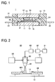
- FIG. 1 is a cross sectional view showing a semiconductor device of the present embodiment.
- This semiconductor device 1 is configured such that a semiconductor element 11 is held between a first electrode 12 and a second electrode 13, and further a block electrode 14 is placed between the semiconductor element 11 and the first electrode 12.
- the first electrode 12 and the second electrode 13 are provided as an emitter electrode or a collector electrode which are main electrodes of the semiconductor element 11, and also function as heat sink or dissipating plates.
- Those electrodes 12 and 13 are therefore made of metal providing good electric conductivity and heat conductivity, such as copper and aluminum.
- the block electrode 14 is integrally formed on the first electrode 12 by a cold spray method.
- a solder layer 15 is provided between the semiconductor element 11 and the block electrode 14 to bond them and a solder layer 16 is provided between the semiconductor element 11 and the second electrode 13 to bond them.
- Main electrode terminals 21 and 22 are connected respectively to the first electrode 12 and the second electrode 13.
- a control electrode terminal 23 is connected to the semiconductor element 11 through a bonding wire 24.
- Those components are wholly sealingly covered with sealing resin 10.
- the first electrode 12 and the second electrode 13 are examples of a substrate recited in claims and are formed, on their surfaces, with resin bonding coats 18 by the cold spray method.
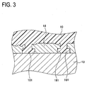
- FIG. 2 is a conceptual diagram showing a structure of a coating device to be used in the cold spray method.
- a coating device 80 includes a compressor 81 for supplying compressed gas. This compressed gas supplied from the compressor 81 is heated in a heating unit 82 and then injected from a nozzle 84 via a pressure regulating valve 83.
- a powder tank 85 stores for example copper powder.
- the nozzle 84 is provided with a heater 86 to further heat the copper powder fed from the powder tank 85 into the nozzle 84.
- a drive unit 87 is provided to move the nozzle 84 in parallel in order to spray the copper powder onto a specified region to form a coat or film thereon.
- a mask 88 is placed on the first electrode 12.
- This mask 88 includes an open frame 881 having a dimension corresponding to the region to be coated.
- the open frame 881 is disposed in place on the first electrode 12.
- Copper powder having average particle diameter of 5 to 60 ⁇ m is supplied from the powder tank 85 to the nozzle 84.
- the copper powder is heated by the heater 86. Further, the compressed gas supplied from the compressor 81 and then heated is supplied into the nozzle 84.
- the copper powder in a solid phase state having been heated to 50°C to 200°C is sprayed swiftly together with the compressed gas onto the surface of the first electrode 12 through the nozzle 84.
- a jet of copper powder in a solid state from the nozzle 84 collides against the first electrode 12 at high velocities ranging from acoustic velocity to supersonic velocity, so that the copper powder is plastically deformed, sticking to the first electrode 12, thereby forming a coat thereon.
- kinetic energy transforms into heat energy. Therefore, powder surfaces exceed a melting point depending on the kinds of materials and bond to the first electrode 12, thereby providing high bonding or adhesion strength.
- two electrodes 12 and 13 are spaced at a fixed distance by the block electrode 14 and sealing resin 10 is filled therebetween.
- the sealing resin 10 hardens and shrinks between the electrodes 12 and 13, the electrodes placed on both surfaces to face each other attempt to come close to each other so as to shorten an interval therebetween, but the block electrode 14 placed therebetween prevents their approaching.
- stress inducing peel-off of the sealing resin 10 acts on bonding boundary surfaces of the resin 10 and the electrodes 12 and 13 and thus the resin 10 is peeled from the electrodes 12 and 13 due to lack of sufficient bonding strength.
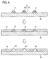
- FIG. 3 is an enlarged cross sectional view showing a part P of FIG. 1 , which is a boundary portion between the second electrode 13 and the sealing resin 10.
- the resin bonding coat 18 is made by the cold spray method and particularly is formed with recesses 181 which are spaces or voids for receiving the sealing resin 10.
- Each of the recesses 181 is formed so that a space is wider in a deep part in a depth direction than in a coat surface part.
- each recess 181 has a stepped shape being narrower on an open surface side, providing a shoulder, so that an anchor portion 101 of the sealing resin 10 having got into and hardened in the recess 181 is hooked on the shoulder without coming off.
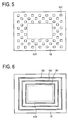
- FIG. 4 is a conceptual diagram showing a process of forming the resin bonding coats 18.
- Forming the resin bonding coats 18 are conducted by first forming two-tiered resist blocks 31 to create spaces or voids for the recesses 181 in a substrate 30 to be used as the first electrode 12 or the second electrode 13. For instance, a photolithographic method is adopted, in which photoresist is applied on the substrate 30 and then an ultraviolet ray is irradiated onto the substrate 30 from above a mask. Thereby, the photoresist of a chemically-changed portion is melted, forming a resist block 31.
- Each resist block 31 is formed of a lower-tier block 311 and an upper-tier block 312 is formed in order so that the lower-tier block 311 has a larger area than the upper-tier block 312.
- the resin bonding coat 18 is formed by the cold spray method using the aforementioned coating device 80. Specifically, copper powder is sprayed onto the substrate 30 to form thereon the resin bonding coat 18 of a predetermined thickness so that the resist blocks 31 are embedded in the coat 18. Thereafter, the resist blocks 31 embedded in the coat 18 are removed by an ashing treatment using oxygen plasma and others. Furthermore, the substrate 30 is subjected to cleaning using a solution such as an acid solution to remove impurities such as metal or organic matters. In the coat 18 from which the resist blocks 31 have been removed in the above way, recesses 181 are formed, each being wider in the deep part in the depth direction than in the open surface part.
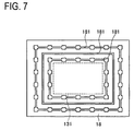
- FIGs. 5 to 7 are plan views showing pattern variations of the recesses formed in the resin bonding coat 18 of the second electrode 13.
- One example of the recesses 181 is a rectangular hole shown in FIG. 5 .
- a plurality of the holes are arranged to surround a bonding region 131 on which the semiconductor element 11 is to be bonded.
- Another example of the recesses 181 may be provided as a plurality of grooves arranged to surround the bonding region 131 as shown in FIG. 6 .
- Further another example of the recesses 181 may also be provided as annular grooves surrounding the bonding region 131 in combination with rectangular holes each having a larger dimension than the groove width, as shown in FIG. 7 .
- the resin bonding coat 18 is formed the surface of each of the first electrode 12 and the second electrode 13 and the sealing resin 10 adheres to the resin bonding coat 18 as shown in FIG. 3 .
- the anchor portions 101 filled in the recesses 181 enhance bonding strength of the sealing resin 10 against the stress that attempts to peel off the sealing resin 10.
- the resin bonding coat 18 formed by the cold spray method is porous and thus has an irregular surface with protrusions and depressions. Accordingly, the sealing resin 10 having got into the recessed portions of the resin bonding coat 18 can contribute to further enhancement of the bonding strength.
- the block electrode 14 is similarly formed by the cold spray method. Thus, the sealing resin 10 can provide higher bonding strength with respect to the block electrode 14.
- the sealing resin 10 entering in each hole spreads all around therein and adheres to the coat 18 defining each hole, thus hooking on to the shoulder. Accordingly, the bonding strength of the sealing resin 10 can be enhanced.
- the sealing resin 10 entering in each recess 181 flows to every corner of each recess 181. Therefore, the sealing resin 10, pushing air bubbles out of the recesses 181, forms the anchor portions 101 filled with resin, thus ensuring bonding strength.
- the recesses 181 each including a groove and holes in combination as shown in FIG.
- the enhanced bonding strength by the resin bonding coat 18 can eliminate the coating of polyamide resin and others conventionally conducted or the forming of sprayed coat such as aluminum. This can reduce a material cost and enhance productivity. Thus, the cost reduction of the semiconductor device 1 can be realized. Since any distortion resulting from a punching process is not caused in forming the recesses 181, the second electrode 13 allows formation of the recesses 181 near the semiconductor element 11.
- the resin bonding coat 18 is formed of metal having good thermal conductivity and electrical conductivity, such as aluminum and copper, and therefore can be formed all over the second electrode 13. Accordingly, the bonding strength between the resin bonding coat 18 and the sealing resin 10 can be ensured at a short distance around the semiconductor element 11.
- the resin bonding coat 18 can be formed easily and uniformly in three dimensions, allowing direct soldering thereon.
- the resin bonding coat 18 is made of copper, nickel, silver, soldering thereto is enabled. Therefore, nickel plating or gold plating conventionally needed for the first and second electrodes 12 and 13 is no longer necessary. Such nickel plating may cause a decrease in bonding strength with the sealing resin. Such gold plating is very expensive. In this respect, the price of the semiconductor device 1 can be reduced.
- FIG. 1 describes the semiconductor device 1 configured to cool both sides.
- the present invention may be applied to a semiconductor device configured to cool one side, in which an electrode is provided on only one side of a semiconductor element.
- FIGs. 5 and 7 exemplify the rectangular hole as the shape of each recess 181. This shape may be circular or others.
Landscapes
- Chemical & Material Sciences (AREA)
- Chemical Kinetics & Catalysis (AREA)
- Engineering & Computer Science (AREA)
- Materials Engineering (AREA)
- Mechanical Engineering (AREA)
- Metallurgy (AREA)
- Organic Chemistry (AREA)
- Structures Or Materials For Encapsulating Or Coating Semiconductor Devices Or Solid State Devices (AREA)
- Encapsulation Of And Coatings For Semiconductor Or Solid State Devices (AREA)
Claims (9)
- Halbleiter (1) aufweisend:ein Halbleiterelement (11);ein einer Fläche des Halbleiterelements zugewandt platziertes Substrat (12, 13); undeine Schicht aus Vergussharz (10), die angeordnet ist, um das Halbleiterelement und einen Abschnitt des Substrates abdichtend abzudecken;wobei das Substrat eine Harzbindeschicht (18) aus kaltgesprühtem Kupfer aufweist, die auf einer dem Vergussharz benachbarten Fläche des Substrates ausgebildet ist, derart, dass die Harzbindeschicht mit dem Vergussharz verbunden ist;wobei die Harzbindeschicht eine Aussparung (181) aufweist, die an einer Grenzfläche zwischen dem Vergussharz und dem Substrat gelegen ist, wobei die Aussparung einen engeren Teil und einen weiteren Teil hat, wobei der weitere Teil benachbart zu dem Substrat gelegen ist; und wobei das Substrat keine Aussparung hat.
- Halbleiter nach Anspruch 1, wobei die Aussparung eine gestufte Form hat.
- Halbleiter nach Anspruch 1 oder 2, wobei das Substrat eine Elektrode ist, die auf einer Fläche des Halbleiterelements platziert ist, und eine Blockelektrode zwischen dem Halbleiterelement und der Elektrode platziert ist, wobei die Blockelektrode durch das Kaltsprühverfahren auf der Elektrode ausgebildet ist.
- Halbleiter nach einem der Ansprüche 1 oder 2, wobei die Aussparung eine Vielzahl von Löchern hat, die um das Halbleiterelement herum angeordnet sind.
- Halbleiter nach einem der Ansprüche 1 oder 2, wobei die Aussparung eine Nut hat, die das Halbleiterelement umgibt.
- Halbleiter nach einem der Ansprüche 1 oder 2, wobei die Aussparung eine Nut, die das Halbleiterelement umgibt, und ein rechteckiges Loch hat, dass die Nut überlappt und eine größere Abmessung als eine Breite der Nut hat.
- Halbleiter nach Anspruch 3, wobei die Aussparung eine Vielzahl von Löcher hat, die um das Halbleiterelement und die Blockelektrode herum angeordnet sind.
- Halbleiter nach Anspruch 3, wobei die Aussparung eine Nut hat, die das Halbleiterelement und die Blockelektrode umgibt.
- Halbleiter nach Anspruch 3, wobei die Aussparung eine Nut, die das Halbleiterelement und die Blockelektrode umgibt, und ein rechteckiges Loch hat, dass die Nut überlappt und eine größere Abmessung als eine Breite der Nut hat.
Applications Claiming Priority (1)
| Application Number | Priority Date | Filing Date | Title |
|---|---|---|---|
| PCT/JP2010/058586 WO2011145202A1 (ja) | 2010-05-21 | 2010-05-21 | 半導体装置 |
Publications (3)
| Publication Number | Publication Date |
|---|---|
| EP2573810A1 EP2573810A1 (de) | 2013-03-27 |
| EP2573810A4 EP2573810A4 (de) | 2014-04-30 |
| EP2573810B1 true EP2573810B1 (de) | 2016-08-17 |
Family
ID=44991326
Family Applications (1)
| Application Number | Title | Priority Date | Filing Date |
|---|---|---|---|
| EP10851766.5A Not-in-force EP2573810B1 (de) | 2010-05-21 | 2010-05-21 | Halbleiterbauelement |
Country Status (6)
| Country | Link |
|---|---|
| US (1) | US8436461B2 (de) |
| EP (1) | EP2573810B1 (de) |
| JP (1) | JP5321601B2 (de) |
| KR (1) | KR101297870B1 (de) |
| CN (1) | CN102652357B (de) |
| WO (1) | WO2011145202A1 (de) |
Families Citing this family (13)
| Publication number | Priority date | Publication date | Assignee | Title |
|---|---|---|---|---|
| CN102549738B (zh) * | 2010-05-18 | 2015-07-01 | 丰田自动车株式会社 | 半导体装置及其制造方法 |
| JP5713032B2 (ja) * | 2013-01-21 | 2015-05-07 | トヨタ自動車株式会社 | 半導体装置の製造方法 |
| KR101748508B1 (ko) * | 2013-01-29 | 2017-06-16 | 도요타지도샤가부시키가이샤 | 전지 |
| JP6037885B2 (ja) | 2013-02-19 | 2016-12-07 | 三菱重工業株式会社 | 成膜方法 |
| JP2015211157A (ja) * | 2014-04-28 | 2015-11-24 | 三菱電機株式会社 | パワー半導体モジュールおよびその製造方法 |
| DE102015201927A1 (de) * | 2015-02-04 | 2016-08-04 | Siemens Aktiengesellschaft | Verfahren zum Kaltgasspritzen mit Maske |
| JP6481409B2 (ja) * | 2015-02-19 | 2019-03-13 | 三菱マテリアル株式会社 | パワーモジュール用基板及びパワーモジュール |
| KR102424402B1 (ko) | 2015-08-13 | 2022-07-25 | 삼성전자주식회사 | 반도체 패키지 및 그 제조방법 |
| USD926234S1 (en) | 2018-05-24 | 2021-07-27 | Whirlpool Corporation | Kitchen appliance with two-dimensional applied surface graphic |
| WO2021193643A1 (ja) * | 2020-03-25 | 2021-09-30 | 国立大学法人東北大学 | 複合部材の製造方法および複合部材 |
| CN115279575B (zh) * | 2020-03-25 | 2026-01-02 | 国立大学法人东北大学 | 复合构件的制造方法及复合构件 |
| JP7680240B2 (ja) * | 2021-03-30 | 2025-05-20 | ローム株式会社 | 半導体装置 |
| KR102866116B1 (ko) | 2021-11-26 | 2025-09-30 | 삼성전자주식회사 | 반도체 패키지 |
Family Cites Families (11)
| Publication number | Priority date | Publication date | Assignee | Title |
|---|---|---|---|---|
| JP2890635B2 (ja) | 1990-03-29 | 1999-05-17 | セイコーエプソン株式会社 | 半導体装置 |
| JPH06112390A (ja) | 1992-09-24 | 1994-04-22 | Nippon Steel Corp | リードフレーム |
| JP4248037B2 (ja) * | 1997-02-04 | 2009-04-02 | 株式会社不二機販 | 金属被膜の形成方法 |
| JP3719506B2 (ja) | 2001-12-19 | 2005-11-24 | 株式会社デンソー | 半導体装置及びその製造方法 |
| JP2002289739A (ja) | 2001-03-23 | 2002-10-04 | Dainippon Printing Co Ltd | 樹脂封止型半導体装置および半導体装置用回路部材とその製造方法 |
| JP3807354B2 (ja) * | 2001-08-06 | 2006-08-09 | 株式会社デンソー | 半導体装置 |
| JP3748849B2 (ja) * | 2002-12-06 | 2006-02-22 | 三菱電機株式会社 | 樹脂封止型半導体装置 |
| JP4595665B2 (ja) | 2005-05-13 | 2010-12-08 | 富士電機システムズ株式会社 | 配線基板の製造方法 |
| JP4657129B2 (ja) * | 2006-03-24 | 2011-03-23 | ローム株式会社 | 半導体装置の製造方法 |
| JP4241859B2 (ja) | 2007-07-19 | 2009-03-18 | トヨタ自動車株式会社 | パワーモジュールの製造方法、パワーモジュール、車両用インバータ、及び車両 |
| KR101438826B1 (ko) * | 2008-06-23 | 2014-09-05 | 엘지이노텍 주식회사 | 발광장치 |
-
2010
- 2010-05-21 CN CN201080055269.XA patent/CN102652357B/zh not_active Expired - Fee Related
- 2010-05-21 KR KR1020127014542A patent/KR101297870B1/ko not_active Expired - Fee Related
- 2010-05-21 JP JP2010544107A patent/JP5321601B2/ja not_active Expired - Fee Related
- 2010-05-21 EP EP10851766.5A patent/EP2573810B1/de not_active Not-in-force
- 2010-05-21 WO PCT/JP2010/058586 patent/WO2011145202A1/ja not_active Ceased
- 2010-05-21 US US13/499,253 patent/US8436461B2/en not_active Expired - Fee Related
Also Published As
| Publication number | Publication date |
|---|---|
| US20120181685A1 (en) | 2012-07-19 |
| CN102652357B (zh) | 2015-09-09 |
| JP5321601B2 (ja) | 2013-10-23 |
| EP2573810A4 (de) | 2014-04-30 |
| KR20120091297A (ko) | 2012-08-17 |
| WO2011145202A1 (ja) | 2011-11-24 |
| JPWO2011145202A1 (ja) | 2013-07-22 |
| US8436461B2 (en) | 2013-05-07 |
| KR101297870B1 (ko) | 2013-08-19 |
| CN102652357A (zh) | 2012-08-29 |
| EP2573810A1 (de) | 2013-03-27 |
Similar Documents
| Publication | Publication Date | Title |
|---|---|---|
| EP2573810B1 (de) | Halbleiterbauelement | |
| EP3340291B1 (de) | Verfahren zur herstellung einer elektronischen modulanordnung und elektronische modulanordnung | |
| US7256431B2 (en) | Insulating substrate and semiconductor device having a thermally sprayed circuit pattern | |
| CN102593091B (zh) | 半导体模块 | |
| JP4844702B1 (ja) | マスキング治具、基板加熱装置、及び成膜方法 | |
| JP5565315B2 (ja) | 半導体装置の製造方法 | |
| US8336202B2 (en) | Method of manufacturing a wiring board | |
| US10181445B2 (en) | Power module | |
| US20120228776A1 (en) | Semiconductor device | |
| JP2005005638A (ja) | 半導体モジュールおよびその製造方法 | |
| JP2013507007A (ja) | 半導体装置およびその形成方法 | |
| JP2013247256A (ja) | 半導体装置およびその製造方法 | |
| CN203038909U (zh) | 半导体模块 | |
| US20150069600A1 (en) | Embedded Silver Nanomaterials into Die Backside to Enhance Package Performance and Reliability | |
| JP2013168421A (ja) | 配線基板および配線基板の製造方法 | |
| CN119725094A (zh) | 一种烧结方法及功率器件 | |
| CN103858225B (zh) | 用于建立钎焊连接的方法 | |
| JP4492257B2 (ja) | 半導体モジュールおよびその製造方法 | |
| CN118266076B (zh) | 金属衬底结构和将端子附接至金属衬底结构的方法以及半导体功率模块 | |
| CN106920791B (zh) | 半导体发光装置及半导体发光装置的制造方法 | |
| WO2024027891A1 (en) | Method for attaching a terminal to a metal substrate structure for a semiconductor power module and semiconductor power module | |
| JP2009076604A (ja) | 熱電変換モジュールの製造方法と熱電変換モジュール | |
| JP2013016603A (ja) | 半導体装置及びその製造方法 | |
| JP2010239164A (ja) | 配線基板 | |
| HK1106067A (zh) | 半導體封裝結構及其製造方法 |
Legal Events
| Date | Code | Title | Description |
|---|---|---|---|
| PUAI | Public reference made under article 153(3) epc to a published international application that has entered the european phase |
Free format text: ORIGINAL CODE: 0009012 |
|
| 17P | Request for examination filed |
Effective date: 20120315 |
|
| AK | Designated contracting states |
Kind code of ref document: A1 Designated state(s): AL AT BE BG CH CY CZ DE DK EE ES FI FR GB GR HR HU IE IS IT LI LT LU LV MC MK MT NL NO PL PT RO SE SI SK SM TR |
|
| DAX | Request for extension of the european patent (deleted) | ||
| REG | Reference to a national code |
Ref country code: DE Ref legal event code: R079 Ref document number: 602010035722 Country of ref document: DE Free format text: PREVIOUS MAIN CLASS: H01L0023120000 Ipc: C23C0024040000 |
|
| A4 | Supplementary search report drawn up and despatched |
Effective date: 20140401 |
|
| RIC1 | Information provided on ipc code assigned before grant |
Ipc: H01L 23/48 20060101ALI20140326BHEP Ipc: H01L 23/495 20060101ALI20140326BHEP Ipc: H01L 23/00 20060101ALI20140326BHEP Ipc: C23C 24/04 20060101AFI20140326BHEP Ipc: H01L 23/051 20060101ALI20140326BHEP Ipc: H01L 23/28 20060101ALI20140326BHEP Ipc: H01L 23/433 20060101ALI20140326BHEP Ipc: C23C 28/00 20060101ALI20140326BHEP Ipc: H01L 23/12 20060101ALI20140326BHEP Ipc: H01L 23/31 20060101ALI20140326BHEP |
|
| 17Q | First examination report despatched |
Effective date: 20141212 |
|
| GRAP | Despatch of communication of intention to grant a patent |
Free format text: ORIGINAL CODE: EPIDOSNIGR1 |
|
| INTG | Intention to grant announced |
Effective date: 20160311 |
|
| GRAS | Grant fee paid |
Free format text: ORIGINAL CODE: EPIDOSNIGR3 |
|
| GRAA | (expected) grant |
Free format text: ORIGINAL CODE: 0009210 |
|
| AK | Designated contracting states |
Kind code of ref document: B1 Designated state(s): AL AT BE BG CH CY CZ DE DK EE ES FI FR GB GR HR HU IE IS IT LI LT LU LV MC MK MT NL NO PL PT RO SE SI SK SM TR |
|
| REG | Reference to a national code |
Ref country code: GB Ref legal event code: FG4D |
|
| REG | Reference to a national code |
Ref country code: CH Ref legal event code: EP |
|
| REG | Reference to a national code |
Ref country code: IE Ref legal event code: FG4D |
|
| REG | Reference to a national code |
Ref country code: AT Ref legal event code: REF Ref document number: 821186 Country of ref document: AT Kind code of ref document: T Effective date: 20160915 |
|
| REG | Reference to a national code |
Ref country code: DE Ref legal event code: R096 Ref document number: 602010035722 Country of ref document: DE |
|
| REG | Reference to a national code |
Ref country code: NL Ref legal event code: MP Effective date: 20160817 |
|
| REG | Reference to a national code |
Ref country code: LT Ref legal event code: MG4D |
|
| REG | Reference to a national code |
Ref country code: AT Ref legal event code: MK05 Ref document number: 821186 Country of ref document: AT Kind code of ref document: T Effective date: 20160817 |
|
| PG25 | Lapsed in a contracting state [announced via postgrant information from national office to epo] |
Ref country code: HR Free format text: LAPSE BECAUSE OF FAILURE TO SUBMIT A TRANSLATION OF THE DESCRIPTION OR TO PAY THE FEE WITHIN THE PRESCRIBED TIME-LIMIT Effective date: 20160817 Ref country code: NO Free format text: LAPSE BECAUSE OF FAILURE TO SUBMIT A TRANSLATION OF THE DESCRIPTION OR TO PAY THE FEE WITHIN THE PRESCRIBED TIME-LIMIT Effective date: 20161117 Ref country code: LT Free format text: LAPSE BECAUSE OF FAILURE TO SUBMIT A TRANSLATION OF THE DESCRIPTION OR TO PAY THE FEE WITHIN THE PRESCRIBED TIME-LIMIT Effective date: 20160817 Ref country code: FI Free format text: LAPSE BECAUSE OF FAILURE TO SUBMIT A TRANSLATION OF THE DESCRIPTION OR TO PAY THE FEE WITHIN THE PRESCRIBED TIME-LIMIT Effective date: 20160817 Ref country code: IT Free format text: LAPSE BECAUSE OF FAILURE TO SUBMIT A TRANSLATION OF THE DESCRIPTION OR TO PAY THE FEE WITHIN THE PRESCRIBED TIME-LIMIT Effective date: 20160817 Ref country code: NL Free format text: LAPSE BECAUSE OF FAILURE TO SUBMIT A TRANSLATION OF THE DESCRIPTION OR TO PAY THE FEE WITHIN THE PRESCRIBED TIME-LIMIT Effective date: 20160817 |
|
| REG | Reference to a national code |
Ref country code: DE Ref legal event code: R084 Ref document number: 602010035722 Country of ref document: DE |
|
| PG25 | Lapsed in a contracting state [announced via postgrant information from national office to epo] |
Ref country code: SE Free format text: LAPSE BECAUSE OF FAILURE TO SUBMIT A TRANSLATION OF THE DESCRIPTION OR TO PAY THE FEE WITHIN THE PRESCRIBED TIME-LIMIT Effective date: 20160817 Ref country code: AT Free format text: LAPSE BECAUSE OF FAILURE TO SUBMIT A TRANSLATION OF THE DESCRIPTION OR TO PAY THE FEE WITHIN THE PRESCRIBED TIME-LIMIT Effective date: 20160817 Ref country code: PL Free format text: LAPSE BECAUSE OF FAILURE TO SUBMIT A TRANSLATION OF THE DESCRIPTION OR TO PAY THE FEE WITHIN THE PRESCRIBED TIME-LIMIT Effective date: 20160817 Ref country code: GR Free format text: LAPSE BECAUSE OF FAILURE TO SUBMIT A TRANSLATION OF THE DESCRIPTION OR TO PAY THE FEE WITHIN THE PRESCRIBED TIME-LIMIT Effective date: 20161118 Ref country code: LV Free format text: LAPSE BECAUSE OF FAILURE TO SUBMIT A TRANSLATION OF THE DESCRIPTION OR TO PAY THE FEE WITHIN THE PRESCRIBED TIME-LIMIT Effective date: 20160817 Ref country code: ES Free format text: LAPSE BECAUSE OF FAILURE TO SUBMIT A TRANSLATION OF THE DESCRIPTION OR TO PAY THE FEE WITHIN THE PRESCRIBED TIME-LIMIT Effective date: 20160817 Ref country code: PT Free format text: LAPSE BECAUSE OF FAILURE TO SUBMIT A TRANSLATION OF THE DESCRIPTION OR TO PAY THE FEE WITHIN THE PRESCRIBED TIME-LIMIT Effective date: 20161219 |
|
| PG25 | Lapsed in a contracting state [announced via postgrant information from national office to epo] |
Ref country code: EE Free format text: LAPSE BECAUSE OF FAILURE TO SUBMIT A TRANSLATION OF THE DESCRIPTION OR TO PAY THE FEE WITHIN THE PRESCRIBED TIME-LIMIT Effective date: 20160817 Ref country code: RO Free format text: LAPSE BECAUSE OF FAILURE TO SUBMIT A TRANSLATION OF THE DESCRIPTION OR TO PAY THE FEE WITHIN THE PRESCRIBED TIME-LIMIT Effective date: 20160817 |
|
| REG | Reference to a national code |
Ref country code: DE Ref legal event code: R097 Ref document number: 602010035722 Country of ref document: DE |
|
| PG25 | Lapsed in a contracting state [announced via postgrant information from national office to epo] |
Ref country code: BG Free format text: LAPSE BECAUSE OF FAILURE TO SUBMIT A TRANSLATION OF THE DESCRIPTION OR TO PAY THE FEE WITHIN THE PRESCRIBED TIME-LIMIT Effective date: 20161117 Ref country code: DK Free format text: LAPSE BECAUSE OF FAILURE TO SUBMIT A TRANSLATION OF THE DESCRIPTION OR TO PAY THE FEE WITHIN THE PRESCRIBED TIME-LIMIT Effective date: 20160817 Ref country code: BE Free format text: LAPSE BECAUSE OF FAILURE TO SUBMIT A TRANSLATION OF THE DESCRIPTION OR TO PAY THE FEE WITHIN THE PRESCRIBED TIME-LIMIT Effective date: 20160817 Ref country code: SK Free format text: LAPSE BECAUSE OF FAILURE TO SUBMIT A TRANSLATION OF THE DESCRIPTION OR TO PAY THE FEE WITHIN THE PRESCRIBED TIME-LIMIT Effective date: 20160817 Ref country code: SM Free format text: LAPSE BECAUSE OF FAILURE TO SUBMIT A TRANSLATION OF THE DESCRIPTION OR TO PAY THE FEE WITHIN THE PRESCRIBED TIME-LIMIT Effective date: 20160817 Ref country code: CZ Free format text: LAPSE BECAUSE OF FAILURE TO SUBMIT A TRANSLATION OF THE DESCRIPTION OR TO PAY THE FEE WITHIN THE PRESCRIBED TIME-LIMIT Effective date: 20160817 |
|
| PLBE | No opposition filed within time limit |
Free format text: ORIGINAL CODE: 0009261 |
|
| STAA | Information on the status of an ep patent application or granted ep patent |
Free format text: STATUS: NO OPPOSITION FILED WITHIN TIME LIMIT |
|
| 26N | No opposition filed |
Effective date: 20170518 |
|
| PG25 | Lapsed in a contracting state [announced via postgrant information from national office to epo] |
Ref country code: LU Free format text: LAPSE BECAUSE OF NON-PAYMENT OF DUE FEES Effective date: 20170531 Ref country code: SI Free format text: LAPSE BECAUSE OF FAILURE TO SUBMIT A TRANSLATION OF THE DESCRIPTION OR TO PAY THE FEE WITHIN THE PRESCRIBED TIME-LIMIT Effective date: 20160817 |
|
| REG | Reference to a national code |
Ref country code: CH Ref legal event code: PL |
|
| GBPC | Gb: european patent ceased through non-payment of renewal fee |
Effective date: 20170521 |
|
| PG25 | Lapsed in a contracting state [announced via postgrant information from national office to epo] |
Ref country code: MC Free format text: LAPSE BECAUSE OF FAILURE TO SUBMIT A TRANSLATION OF THE DESCRIPTION OR TO PAY THE FEE WITHIN THE PRESCRIBED TIME-LIMIT Effective date: 20160817 |
|
| REG | Reference to a national code |
Ref country code: IE Ref legal event code: MM4A |
|
| PG25 | Lapsed in a contracting state [announced via postgrant information from national office to epo] |
Ref country code: LI Free format text: LAPSE BECAUSE OF NON-PAYMENT OF DUE FEES Effective date: 20170531 Ref country code: CH Free format text: LAPSE BECAUSE OF NON-PAYMENT OF DUE FEES Effective date: 20170531 |
|
| REG | Reference to a national code |
Ref country code: FR Ref legal event code: ST Effective date: 20180131 |
|
| PG25 | Lapsed in a contracting state [announced via postgrant information from national office to epo] |
Ref country code: LU Free format text: LAPSE BECAUSE OF NON-PAYMENT OF DUE FEES Effective date: 20170521 |
|
| PG25 | Lapsed in a contracting state [announced via postgrant information from national office to epo] |
Ref country code: GB Free format text: LAPSE BECAUSE OF NON-PAYMENT OF DUE FEES Effective date: 20170521 Ref country code: IE Free format text: LAPSE BECAUSE OF NON-PAYMENT OF DUE FEES Effective date: 20170521 |
|
| PG25 | Lapsed in a contracting state [announced via postgrant information from national office to epo] |
Ref country code: FR Free format text: LAPSE BECAUSE OF NON-PAYMENT OF DUE FEES Effective date: 20170531 |
|
| PG25 | Lapsed in a contracting state [announced via postgrant information from national office to epo] |
Ref country code: MT Free format text: LAPSE BECAUSE OF NON-PAYMENT OF DUE FEES Effective date: 20170521 |
|
| PG25 | Lapsed in a contracting state [announced via postgrant information from national office to epo] |
Ref country code: AL Free format text: LAPSE BECAUSE OF FAILURE TO SUBMIT A TRANSLATION OF THE DESCRIPTION OR TO PAY THE FEE WITHIN THE PRESCRIBED TIME-LIMIT Effective date: 20160817 |
|
| PG25 | Lapsed in a contracting state [announced via postgrant information from national office to epo] |
Ref country code: HU Free format text: LAPSE BECAUSE OF FAILURE TO SUBMIT A TRANSLATION OF THE DESCRIPTION OR TO PAY THE FEE WITHIN THE PRESCRIBED TIME-LIMIT; INVALID AB INITIO Effective date: 20100521 |
|
| PG25 | Lapsed in a contracting state [announced via postgrant information from national office to epo] |
Ref country code: CY Free format text: LAPSE BECAUSE OF NON-PAYMENT OF DUE FEES Effective date: 20160817 |
|
| PG25 | Lapsed in a contracting state [announced via postgrant information from national office to epo] |
Ref country code: MK Free format text: LAPSE BECAUSE OF FAILURE TO SUBMIT A TRANSLATION OF THE DESCRIPTION OR TO PAY THE FEE WITHIN THE PRESCRIBED TIME-LIMIT Effective date: 20160817 |
|
| PG25 | Lapsed in a contracting state [announced via postgrant information from national office to epo] |
Ref country code: TR Free format text: LAPSE BECAUSE OF FAILURE TO SUBMIT A TRANSLATION OF THE DESCRIPTION OR TO PAY THE FEE WITHIN THE PRESCRIBED TIME-LIMIT Effective date: 20160817 |
|
| REG | Reference to a national code |
Ref country code: DE Ref legal event code: R082 Ref document number: 602010035722 Country of ref document: DE Representative=s name: TBK, DE Ref country code: DE Ref legal event code: R081 Ref document number: 602010035722 Country of ref document: DE Owner name: DENSO CORPORATION, KARIYA-CITY, JP Free format text: FORMER OWNER: TOYOTA JIDOSHA KABUSHIKI KAISHA, TOYOTA-SHI, AICHI-KEN, JP |
|
| PG25 | Lapsed in a contracting state [announced via postgrant information from national office to epo] |
Ref country code: IS Free format text: LAPSE BECAUSE OF FAILURE TO SUBMIT A TRANSLATION OF THE DESCRIPTION OR TO PAY THE FEE WITHIN THE PRESCRIBED TIME-LIMIT Effective date: 20161217 |
|
| PGFP | Annual fee paid to national office [announced via postgrant information from national office to epo] |
Ref country code: DE Payment date: 20210520 Year of fee payment: 12 |
|
| REG | Reference to a national code |
Ref country code: DE Ref legal event code: R119 Ref document number: 602010035722 Country of ref document: DE |
|
| PG25 | Lapsed in a contracting state [announced via postgrant information from national office to epo] |
Ref country code: DE Free format text: LAPSE BECAUSE OF NON-PAYMENT OF DUE FEES Effective date: 20221201 |