EP2574687A2 - Procédé et dispositif destinés au revêtement galvanisé de substrats - Google Patents
Procédé et dispositif destinés au revêtement galvanisé de substrats Download PDFInfo
- Publication number
- EP2574687A2 EP2574687A2 EP12199607A EP12199607A EP2574687A2 EP 2574687 A2 EP2574687 A2 EP 2574687A2 EP 12199607 A EP12199607 A EP 12199607A EP 12199607 A EP12199607 A EP 12199607A EP 2574687 A2 EP2574687 A2 EP 2574687A2
- Authority
- EP
- European Patent Office
- Prior art keywords
- substrate
- coating
- coating liquid
- pulses
- light
- Prior art date
- Legal status (The legal status is an assumption and is not a legal conclusion. Google has not performed a legal analysis and makes no representation as to the accuracy of the status listed.)
- Withdrawn
Links
Images


Classifications
-
- C—CHEMISTRY; METALLURGY
- C25—ELECTROLYTIC OR ELECTROPHORETIC PROCESSES; APPARATUS THEREFOR
- C25D—PROCESSES FOR THE ELECTROLYTIC OR ELECTROPHORETIC PRODUCTION OF COATINGS; ELECTROFORMING; APPARATUS THEREFOR
- C25D5/00—Electroplating characterised by the process; Pretreatment or after-treatment of workpieces
- C25D5/18—Electroplating using modulated, pulsed or reversing current
-
- C—CHEMISTRY; METALLURGY
- C25—ELECTROLYTIC OR ELECTROPHORETIC PROCESSES; APPARATUS THEREFOR
- C25D—PROCESSES FOR THE ELECTROLYTIC OR ELECTROPHORETIC PRODUCTION OF COATINGS; ELECTROFORMING; APPARATUS THEREFOR
- C25D17/00—Constructional parts, or assemblies thereof, of cells for electrolytic coating
- C25D17/001—Apparatus specially adapted for electrolytic coating of wafers, e.g. semiconductors or solar cells
-
- C—CHEMISTRY; METALLURGY
- C25—ELECTROLYTIC OR ELECTROPHORETIC PROCESSES; APPARATUS THEREFOR
- C25D—PROCESSES FOR THE ELECTROLYTIC OR ELECTROPHORETIC PRODUCTION OF COATINGS; ELECTROFORMING; APPARATUS THEREFOR
- C25D21/00—Processes for servicing or operating cells for electrolytic coating
- C25D21/12—Process control or regulation
-
- C—CHEMISTRY; METALLURGY
- C25—ELECTROLYTIC OR ELECTROPHORETIC PROCESSES; APPARATUS THEREFOR
- C25D—PROCESSES FOR THE ELECTROLYTIC OR ELECTROPHORETIC PRODUCTION OF COATINGS; ELECTROFORMING; APPARATUS THEREFOR
- C25D5/00—Electroplating characterised by the process; Pretreatment or after-treatment of workpieces
- C25D5/011—Electroplating using electromagnetic wave irradiation
-
- C—CHEMISTRY; METALLURGY
- C25—ELECTROLYTIC OR ELECTROPHORETIC PROCESSES; APPARATUS THEREFOR
- C25D—PROCESSES FOR THE ELECTROLYTIC OR ELECTROPHORETIC PRODUCTION OF COATINGS; ELECTROFORMING; APPARATUS THEREFOR
- C25D5/00—Electroplating characterised by the process; Pretreatment or after-treatment of workpieces
- C25D5/08—Electroplating with moving electrolyte e.g. jet electroplating
-
- C—CHEMISTRY; METALLURGY
- C25—ELECTROLYTIC OR ELECTROPHORETIC PROCESSES; APPARATUS THEREFOR
- C25D—PROCESSES FOR THE ELECTROLYTIC OR ELECTROPHORETIC PRODUCTION OF COATINGS; ELECTROFORMING; APPARATUS THEREFOR
- C25D7/00—Electroplating characterised by the article coated
- C25D7/12—Semiconductors
- C25D7/123—Semiconductors first coated with a seed layer or a conductive layer
- C25D7/126—Semiconductors first coated with a seed layer or a conductive layer for solar cells
-
- H—ELECTRICITY
- H10—SEMICONDUCTOR DEVICES; ELECTRIC SOLID-STATE DEVICES NOT OTHERWISE PROVIDED FOR
- H10F—INORGANIC SEMICONDUCTOR DEVICES SENSITIVE TO INFRARED RADIATION, LIGHT, ELECTROMAGNETIC RADIATION OF SHORTER WAVELENGTH OR CORPUSCULAR RADIATION
- H10F77/00—Constructional details of devices covered by this subclass
- H10F77/20—Electrodes
- H10F77/206—Electrodes for devices having potential barriers
- H10F77/211—Electrodes for devices having potential barriers for photovoltaic cells
-
- Y—GENERAL TAGGING OF NEW TECHNOLOGICAL DEVELOPMENTS; GENERAL TAGGING OF CROSS-SECTIONAL TECHNOLOGIES SPANNING OVER SEVERAL SECTIONS OF THE IPC; TECHNICAL SUBJECTS COVERED BY FORMER USPC CROSS-REFERENCE ART COLLECTIONS [XRACs] AND DIGESTS
- Y02—TECHNOLOGIES OR APPLICATIONS FOR MITIGATION OR ADAPTATION AGAINST CLIMATE CHANGE
- Y02E—REDUCTION OF GREENHOUSE GAS [GHG] EMISSIONS, RELATED TO ENERGY GENERATION, TRANSMISSION OR DISTRIBUTION
- Y02E10/00—Energy generation through renewable energy sources
- Y02E10/50—Photovoltaic [PV] energy
Definitions
- the invention relates to a device for galvanic coating of at least one surface of at least one substrate according to the preamble of patent claim 1.
- the invention also relates to a process for electroplating according to the preamble of patent claim 8.
- the coating can be carried out only light-induced but also current-assisted.
- the light radiation by means of light generates a voltage at the cell, which sets a cell current in motion.
- This cell flow initiates a metal deposition from the appropriately composed coating bath on the front side of the solar cell.
- the solar cell is the cathode in the electroplating circuit, which is called the rectifier circuit.
- the objects to be electroplated are on the way through the coating bath substantially in the same electric field.
- the plating speed ie the speed with which However, the deposited metal layer builds up on the substrates, but is relatively low. This means that at a given speed of movement of the objects, the length of the device must be very large.
- the object of the invention is to further increase the throughput of substrates in the coating apparatus.
- the object is achieved with a device according to claim 1 and a method according to claim 8.
- the device is characterized in that means for generating synchronous current pulses and light pulses are provided, wherein in the pauses between the current pulses, the irradiation of the substrate is interrupted.
- the throughput can be increased if one works not only with current pulses but also with light pulses synchronous with the current pulses. Synchronous pulses means that the light pulses are always present when the current pulses are present. In the pulse pauses between the current pulses are also the pulse pauses of the light pulses.
- the light source can be switched off. Shading of the light source in the breaks is also possible. LEDs are preferably used as light sources.
- the means for synchronously generating current pulses and pulses comprises at least one pulse generator in the rectifier circuit and / or in the light source circuit.
- the rectifier circuit and / or the light source circuit are preferably connected to the pulse generator.
- a pulse generator may preferably be provided a pulse generator to which both circuits are connected. Also, a separate pulse generator can be provided in each circuit, which are interconnected according to the generation of synchronous pulses.
- the Lichtcluellenschaftnik is coupled via an optocoupler to the rectifier circuit.
- the coupling via an opto-coupler has the advantage, due to the galvanic isolation of input and output, that interference from one circuit can not be transferred to the other circuit.
- the combination of the circuits via an optocoupler thus has the advantage of greater stability and uniformity of the pulses generated.
- the light source circuit and / or rectifier circuit has at least one control device which controls the light output of the light source and / or the intensity of the current pulses as a function of the length of the current pulses and / or the light pulses.
- the morphology of the deposited metal layers can be influenced via the strength of the light pulses and / or the current pulses. Graded metal layers with optimized properties can be deposited. Another possibility is z. B. in the same time to change the strength of both the light pulses and the current pulses by z. B. the current pulses are lowered during the coating and the light pulses are increased simultaneously.
- means for generating a flow of the coating liquid are preferably provided. Since the substrates are moved by the quiescent coating liquid, a flow is already present on the surfaces of the substrate. By means of the coating liquid should also be added to flow, so that an additional flow is generated at the surface of the substrate to the already existing due to the substrate movement flow.
- the throughput can be increased by increasing the current density, z. B. by the strength of the current pulses, because thereby the achievable layer thickness is deposited faster.
- the current density can not be chosen arbitrarily high, because the so-called limiting current density must be observed.
- the limiting current density is understood to be the current density at which the free metal ion concentration at the cathode surface to be coated approaches zero.
- At least one nozzle is provided for introducing coating liquid.
- the coating liquid is mixed into a turbulent flow, which is preferably chosen to be so large that it outweighs or intensifies the flow caused by the advance of the substrate by the coating liquid on the surface to be coated.
- the nozzle is arranged in the coating bath opposite the surface to be coated.
- the nozzle is preferably directed perpendicular to the surface to be coated of the substrate.
- a flow is directed onto the surface of the substrate to be coated so that vortices are generated when the flow hits the substrate.
- These vortices should have a speed at the surface of the substrate which is greater than the relative speed of the coating liquid due to the advancement of the substrate.
- the nozzle is disposed between the anodes of the rectifier circuit.
- the coating liquid arising from the nozzles can flow unimpeded to the surface to be coated and is not attenuated by the anodes.
- the nozzle is preferably a Venturi nozzle with which a high exit velocity of the coating liquid can be achieved.
- the means for generating the flow of the coating liquid comprise a circulation device.
- This circulation device is preferably a countercurrent device.
- the countercurrent device puts the coating liquid in a flow which is directed counter to the feed direction of the substrate in the coating bath.
- the inlet of the coating trough is preferably arranged at the end and the outlet of the coating trough at the beginning of the conveying device.
- the coating liquid is thus preferably sucked out of the coating trough counter to the feed direction.
- inlet and outlet are in the height of the transport device, d. H. arranged in the height of the substrates to be transported, so that the counterflow is not hindered by the other internals in the coating.
- the device with nozzles can also be used alone as the circulation device. However, it is preferred to provide both devices in combination.
- the method for galvanic coating of at least one surface of a substrate is characterized in that the galvanic current and the light are pulsed synchronously, wherein in the pulse intervals between the current pulses, the irradiation of the substrate is interrupted.
- the length of the light and current pulses is preferably 0.1 ms to 10000 ms.
- Preferred pulse lengths are 1 ms to 1000 ms, in particular 1 ms to 100 ms.
- the length of the pulses is preferably chosen to be equal to the length of the pulse pauses.
- the current pulses and / or the light pulses are preferably rectangular pulses.
- the strength and / or the length of the light pulses and / or the current pulses can be changed.
- the change of the pulses allows the deposition of z. B. graded metal layers with optimized properties.
- individual galvanization programs can be realized in this way.
- the light output may be 10% of the maximum light output if the pulse length is 100 ms, 20% for a pulse length of 1 ms and 80% for a pulse length of 0.5 ms.
- a DC current may be applied in the pauses of the current pulses whose intensity is preferably I 2 ⁇ 0.5 ⁇ I 1 , where I 1 denotes the magnitude of the current pulses.
- the current intensity I 2 is preferably selected to be so low that the necessary regeneration of the electrolytic coating liquid with respect to the metal ion concentration at the cathode surface to be coated is not impaired.
- the coating liquid is preferably offset at least in the region of the surface of the substrate to be coated in a direction opposite to the feed direction of the substrate flow.
- the coating liquid can be at least in the region of the surface to be coated of the substrate to turbulence.
- FIG. 1 schematically a section through a device 10 for coating substrates 1 is shown.
- substrates 1 solar cells 1a are used in the present example.
- the apparatus 10 includes a coating tray 12 containing a coating bath 13 formed from an electrolytic coating liquid 14.
- a transport device 15 is provided which comprises upper transport rollers 16 and lower transport rollers 18, between which the solar cells 1a are held and transported in the direction of the arrow 5.
- the coating trough 12 is filled with the coating liquid 14 so far that the solar cells 1a to be coated are completely in the coating bath 13.
- a circulation device 30 which has a first liquid line 36.
- the coating trough 12 has below the transport device 15 a first outlet 22 to which the first liquid line 36 is connected.
- a first pump 32 arranged in this first liquid line 36, the coating liquid 14 is pumped out of the coating trough 12 via the first outlet 22 and returned to the coating trough 12 via a first inlet 20, which is arranged in the bottom area of the coating trough 12.
- an inflow system 40 having a feed tube 42 is connected to the first fluid line 36.
- a horizontally disposed manifold 44 is connected to which a plurality of venturi 46 is arranged.
- venturi 46 are aligned vertically and thus arranged perpendicular to the solar cell 1 a. From these Venturi nozzles 46, the supplied coating liquid exits at high speed and thus strikes substantially perpendicular to the facing down facing front side 3 of the solar cell 1 a (s. Fig. 2 ).
- venturi 46 are disposed between the anodes 54 of the rectifier circuit 50 (s. Fig. 2 ).
- light sources 64 are located, which are LED light strips. The arrangement of the light strips is shown only schematically. In particular on the surface 3 of the solar cells 1a, this flow coming from below leads to turbulences, so that the coating liquid 14 can quickly regenerate in the region of the surface 3 to be coated in the pulse pauses.
- the coating trough 12 has in the lower left region a second outlet 23, to which a second liquid line 38 is connected to a second pump 34.
- This line 38 opens into a second inlet 21 in the upper region of the coating trough 12.
- the second inlet 21 is located in the region of the solar cells 1 a, so that between the second inlet 21 and the first outlet 22 is a horizontal flow against the feed direction 5 is generated.
- the device 10 may for example be equipped without the second fluid line 38.
- a further variant can be designed without inflow system 40 with and without second fluid line 38.
- the first liquid line 36 is preferably connected to the coating trough 12 at the second inlet 21.
- a solar cell 1 a shown enlarged in section. This has on the back 2 a metallization and on the front side 3 for the formation of contact fingers strips of a suitable paste 4.
- screen printing pastes are preferably used. In galvanic deposition, the metal is deposited from the electrolytic coating liquid only in the area of these screen printing pastes.
- the upper transport rollers 16 contact the metallic back 2 of the solar cell 1 a and can thus be used for applying a galvanic current.
- a rectifier circuit 50 is provided, which connects one of the upper transport rollers 16 with the anodes 54, which are preferably silver anodes.
- the rectifier circuit 50 is a voltage source 52 and a pulse generator 53. By means of the pulse generator 53, current pulses can be applied to the solar cell 1a and the anodes 54.
- a light source 64 for irradiation of the surface 3 to be coated representative of a plurality of light sources, a light source 64, z. As an LED, located. This light source 64 is connected to a light source circuit 60 having a power supply 62.
- the two circuits 50 and 60 are interconnected via an optocoupler 56, wherein the input 57 of the optocoupler 56 is connected to the rectifier circuit 50 and the output 58 to the light source circuit 60th
- the optocoupler 56 is switched in such a way that when a current pulse is applied, the light source 64 is switched on at the same time, so that a light pulse is generated at the same time. In the power pulse pauses, the light source 64 is turned off.
- Fig. 3 another embodiment is shown in which no optocoupler 56 is provided. Instead, the light source circuit 60 is connected directly to the pulse generator 53, which thus prescribes the pulses for both circuits 50, 60.
- a control device 66 may be arranged in the light source circuit 60. This control device 66 can control the light pulse strength, for example, as a function of the length of the pulses.
- a control device 59 may be provided, are set with the different lengths and heights of the current pulses.
- both control devices 59, 66 a fully automatic galvanization program with individual coating stages can be realized. This is particularly advantageous for forming graded layers on the electrode structures defined by the paste 4.
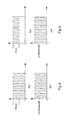
- Fig. 4 Two diagrams are shown with respect to the current pulses and the light pulses.
- the light pulses and the current pulses are the same length. Between the current pulses or the light pulses pauses are provided, which are the same length as the pulses.
- the light and current pulses are completely synchronous, with the light intensity being zero in the pulse pauses. This can be achieved by switching off the light source or by shading the light source.
- a further embodiment is shown in which in the current pulse pauses a direct current is applied, which has the current intensity I 1 .
- the current I 1 is 50% of the current I 2 .
- the light pulses correspond to those from the Fig. 4 ,
Landscapes
- Chemical & Material Sciences (AREA)
- Engineering & Computer Science (AREA)
- Chemical Kinetics & Catalysis (AREA)
- Electrochemistry (AREA)
- Materials Engineering (AREA)
- Metallurgy (AREA)
- Organic Chemistry (AREA)
- Life Sciences & Earth Sciences (AREA)
- Sustainable Development (AREA)
- Physics & Mathematics (AREA)
- Electromagnetism (AREA)
- Automation & Control Theory (AREA)
- Electroplating Methods And Accessories (AREA)
- Photovoltaic Devices (AREA)
Applications Claiming Priority (2)
| Application Number | Priority Date | Filing Date | Title |
|---|---|---|---|
| DE102009029551A DE102009029551B4 (de) | 2009-09-17 | 2009-09-17 | Verfahren und Vorrichtung zur galvanischen Beschichtung von Substraten |
| EP10176929.7A EP2298965B1 (fr) | 2009-09-17 | 2010-09-15 | Procédé et dispositif destinés au revêtement galvanisé de cellules photovoltaïques |
Related Parent Applications (2)
| Application Number | Title | Priority Date | Filing Date |
|---|---|---|---|
| EP10176929.7A Division-Into EP2298965B1 (fr) | 2009-09-17 | 2010-09-15 | Procédé et dispositif destinés au revêtement galvanisé de cellules photovoltaïques |
| EP10176929.7 Division | 2010-09-15 |
Publications (2)
| Publication Number | Publication Date |
|---|---|
| EP2574687A2 true EP2574687A2 (fr) | 2013-04-03 |
| EP2574687A3 EP2574687A3 (fr) | 2013-05-01 |
Family
ID=43413437
Family Applications (2)
| Application Number | Title | Priority Date | Filing Date |
|---|---|---|---|
| EP12199607.8A Withdrawn EP2574687A3 (fr) | 2009-09-17 | 2010-09-15 | Procédé et dispositif destinés au revêtement galvanisé de substrats |
| EP10176929.7A Not-in-force EP2298965B1 (fr) | 2009-09-17 | 2010-09-15 | Procédé et dispositif destinés au revêtement galvanisé de cellules photovoltaïques |
Family Applications After (1)
| Application Number | Title | Priority Date | Filing Date |
|---|---|---|---|
| EP10176929.7A Not-in-force EP2298965B1 (fr) | 2009-09-17 | 2010-09-15 | Procédé et dispositif destinés au revêtement galvanisé de cellules photovoltaïques |
Country Status (7)
| Country | Link |
|---|---|
| US (1) | US20110062028A1 (fr) |
| EP (2) | EP2574687A3 (fr) |
| JP (1) | JP2011066425A (fr) |
| KR (1) | KR20110030408A (fr) |
| CN (1) | CN102021636A (fr) |
| DE (1) | DE102009029551B4 (fr) |
| TW (1) | TW201132808A (fr) |
Families Citing this family (16)
| Publication number | Priority date | Publication date | Assignee | Title |
|---|---|---|---|---|
| US8352155B2 (en) * | 2009-05-21 | 2013-01-08 | Deere & Company | Engine for an agricultural harvester having isochronous torque curve with power bulge |
| DE102009051688A1 (de) * | 2009-10-23 | 2011-04-28 | Fraunhofer-Gesellschaft zur Förderung der angewandten Forschung e.V. | Verfahren zur lichtinduzierten galvanischen Pulsabscheidung zur Ausbildung einer Saatschicht für einen Metallkontakt einer Solarzelle und zur nachfolgenden Verstärkung dieser Saatschicht bzw. dieses Metallkontakts sowie Anordnung zur Durchführung des Verfahrens |
| CN103160908A (zh) * | 2011-12-09 | 2013-06-19 | 财团法人金属工业研究发展中心 | 电沉积装置及其加工机 |
| KR101449942B1 (ko) * | 2012-01-17 | 2014-10-17 | 주식회사 호진플라텍 | 전기도금 및 광 유도 도금을 병행하는 태양전지 기판용 도금장치 및 도금 방법 |
| CN103374737A (zh) * | 2012-04-27 | 2013-10-30 | 库特勒自动化系统(苏州)有限公司 | 太阳能电池电镀装置 |
| CN104178787A (zh) * | 2013-05-26 | 2014-12-03 | 无锡尚德太阳能电力有限公司 | 一种太阳电池镀膜设备以及镀膜方法 |
| US11932960B2 (en) * | 2013-11-26 | 2024-03-19 | Arizona Board Of Regents On Behalf Of Arizona State University | Light-induced aluminum plating on silicon for solar cell metallization |
| WO2015081077A1 (fr) | 2013-11-26 | 2015-06-04 | Arizona Board Of Regents On Behalf Of Arizona State University | Piles solaires formées au moyen d'un placage électrolytique d'aluminium |
| CN105590987B (zh) * | 2014-10-20 | 2022-06-14 | 苏州易益新能源科技有限公司 | 一种水平电化学沉积金属的方法 |
| CN106531817A (zh) * | 2015-09-08 | 2017-03-22 | 英属开曼群岛商精曜有限公司 | 半导体元件及其制作方法 |
| EP3485068B1 (fr) | 2016-07-13 | 2026-04-08 | Iontra Inc | Procédés, dispositifs et compositions électrochimiques |
| KR102010674B1 (ko) | 2017-12-29 | 2019-08-13 | 문석현 | 자동화 부품 선별장치 |
| BE1027567B1 (fr) * | 2019-09-11 | 2021-04-06 | Diarotech Sa | Procédé et dispositif de synthèse de diamant et toutes autres formes allotropiques de carbone par synthèse en phase liquide |
| CN110923761B (zh) * | 2019-12-26 | 2022-01-11 | 重庆切普电子技术有限公司 | 一种喷淋电镀系统 |
| DE102021123280B4 (de) * | 2021-09-08 | 2023-04-13 | Hanwha Q Cells Gmbh | Anlage zur elektrischen Kontaktierung von Wafersolarzellen, Inline-Produktionsvorrichtung und Herstellungsverfahren für eine Wafersolarzelle |
| CN117265609B (zh) * | 2023-11-20 | 2024-04-09 | 圆周率半导体(南通)有限公司 | 一种提升pcb板填孔电镀镀铜均匀性的电镀设备及方法 |
Citations (2)
| Publication number | Priority date | Publication date | Assignee | Title |
|---|---|---|---|---|
| DE4225961A1 (de) | 1992-08-06 | 1994-02-10 | Hoellmueller Maschbau H | Vorrichtung zur Galvanisierung, insbesondere Verkupferung, flacher platten- oder bogenförmiger Gegenstände |
| DE102007038120A1 (de) | 2007-07-31 | 2009-02-05 | Gebr. Schmid Gmbh & Co. | Verfahren zur Beschichtung von Solarzellen sowie Vorrichtung hierfür |
Family Cites Families (15)
| Publication number | Priority date | Publication date | Assignee | Title |
|---|---|---|---|---|
| DE1918354B2 (de) * | 1969-04-11 | 1970-11-26 | Licentia Gmbh | Anordnung zur gleichmaessigen galvanischen Beschichtung langgestreckter stromdurchflossener Kathoden |
| US3975242A (en) * | 1972-11-28 | 1976-08-17 | Nippon Steel Corporation | Horizontal rectilinear type metal-electroplating method |
| JPS5817274B2 (ja) * | 1977-09-01 | 1983-04-06 | 株式会社井上ジャパックス研究所 | 電着加工方法 |
| US4217183A (en) * | 1979-05-08 | 1980-08-12 | International Business Machines Corporation | Method for locally enhancing electroplating rates |
| US4251327A (en) * | 1980-01-14 | 1981-02-17 | Motorola, Inc. | Electroplating method |
| US4608138A (en) * | 1984-02-16 | 1986-08-26 | Mitsubishi Denki Kabushiki Kaisha | Electrolytic method and apparatus |
| JPH06228791A (ja) * | 1992-12-07 | 1994-08-16 | Ebara Yuujiraito Kk | 電気めっき装置 |
| US5599437A (en) * | 1995-06-20 | 1997-02-04 | Faraday Technology, Inc. | Electrolysis of electroactive species using pulsed current |
| US6265020B1 (en) * | 1999-09-01 | 2001-07-24 | Shipley Company, L.L.C. | Fluid delivery systems for electronic device manufacture |
| CN1566406A (zh) * | 2003-06-24 | 2005-01-19 | 天津市磁强技术发展有限公司 | 钕铁硼永磁体的焦磷酸盐脉冲电镀铜方法 |
| DE102005005095A1 (de) * | 2005-02-04 | 2006-08-10 | Höllmüller Maschinenbau GmbH | Verfahren und Vorrichtung zur elektrochemischen Behandlung von Bauteilen in Durchlaufanlagen |
| DE102005038450A1 (de) * | 2005-08-03 | 2007-02-08 | Gebr. Schmid Gmbh & Co. | Einrichtung zur Behandlung von Substraten, insbesondere zur Galvanisierung von Substraten |
| KR20090057449A (ko) * | 2006-09-24 | 2009-06-05 | 쇼킹 테크놀로지스 인코포레이티드 | 전압 절환형 유전 물질 및 광-보조를 이용한 기판 장치 도금 기술 |
| US20080092947A1 (en) * | 2006-10-24 | 2008-04-24 | Applied Materials, Inc. | Pulse plating of a low stress film on a solar cell substrate |
| DE102008053621B4 (de) * | 2008-10-29 | 2010-09-16 | Albert-Ludwigs-Universität Freiburg | Verfahren zur lichtinduzierten galvanischen Pulsabscheidung zur Verstärkung von Metallkontakten von Solarzellen, Anordnung zur Durchführung des Verfahrens und Verwendung |
-
2009
- 2009-09-17 DE DE102009029551A patent/DE102009029551B4/de not_active Expired - Fee Related
-
2010
- 2010-09-15 TW TW099131151A patent/TW201132808A/zh unknown
- 2010-09-15 EP EP12199607.8A patent/EP2574687A3/fr not_active Withdrawn
- 2010-09-15 EP EP10176929.7A patent/EP2298965B1/fr not_active Not-in-force
- 2010-09-16 US US12/883,551 patent/US20110062028A1/en not_active Abandoned
- 2010-09-17 JP JP2010209121A patent/JP2011066425A/ja active Pending
- 2010-09-17 CN CN2010102874401A patent/CN102021636A/zh active Pending
- 2010-09-17 KR KR1020100091668A patent/KR20110030408A/ko not_active Withdrawn
Patent Citations (2)
| Publication number | Priority date | Publication date | Assignee | Title |
|---|---|---|---|---|
| DE4225961A1 (de) | 1992-08-06 | 1994-02-10 | Hoellmueller Maschbau H | Vorrichtung zur Galvanisierung, insbesondere Verkupferung, flacher platten- oder bogenförmiger Gegenstände |
| DE102007038120A1 (de) | 2007-07-31 | 2009-02-05 | Gebr. Schmid Gmbh & Co. | Verfahren zur Beschichtung von Solarzellen sowie Vorrichtung hierfür |
Also Published As
| Publication number | Publication date |
|---|---|
| CN102021636A (zh) | 2011-04-20 |
| EP2298965A2 (fr) | 2011-03-23 |
| EP2298965B1 (fr) | 2014-11-26 |
| TW201132808A (en) | 2011-10-01 |
| JP2011066425A (ja) | 2011-03-31 |
| EP2574687A3 (fr) | 2013-05-01 |
| DE102009029551B4 (de) | 2013-12-24 |
| EP2298965A3 (fr) | 2012-07-04 |
| KR20110030408A (ko) | 2011-03-23 |
| US20110062028A1 (en) | 2011-03-17 |
| DE102009029551A1 (de) | 2011-03-24 |
Similar Documents
| Publication | Publication Date | Title |
|---|---|---|
| EP2298965B1 (fr) | Procédé et dispositif destinés au revêtement galvanisé de cellules photovoltaïques | |
| EP1688518B1 (fr) | Procédé et appareil pour l'électroplacage en continu de pieces | |
| DE102007026633B4 (de) | Vorrichtung und Verfahren zum elektrolytischen Behandeln von plattenförmiger Ware | |
| EP0254962B1 (fr) | Dispositif pour l'électroplacage des articles en forme de plaques, en particulier des plaques de circuits imprimés | |
| DE3228292C2 (fr) | ||
| EP1051886A2 (fr) | Dispositif de traitement electrolytique de carte de circuits et de feuilles conductrices | |
| EP0039453B1 (fr) | Dispositif d'électrodéposition | |
| DE3423033C2 (de) | Maschine zum Vergolden der Lamellenkontakte gedruckter Schaltungen | |
| WO2010130786A2 (fr) | Procédé et dispositif de traitement d'une plaquette | |
| AT392090B (de) | Vorrichtung zum elektroplattieren | |
| EP0030334A1 (fr) | Appareil d'électrolyse pour le renforcement galvanique de feuilles en matière synthétique sous forme de bandes préalablement revêtues d'une couche conductrice | |
| DE19633797B4 (de) | Vorrichtung zum Galvanisieren von elektronischen Leiterplatten oder dergleichen | |
| EP0699781B1 (fr) | Procédé électrolytique de traitement en particulier de revêtement en continu d'un substrat | |
| EP0100400B1 (fr) | Procédé pour le dépôt électrolytique de métaux à partir de solutions aqueuses de sels métalliques sur un ruban d'acier et appareil pour la mise en oeuvre du procédé | |
| DE60302560T2 (de) | Durchlaufmetallisierungsanlage und verfahren zum elektrolytischen metallisieren von werkstücken | |
| DE3011005A1 (de) | Vorrichtung und verfahren zum aufbringen eines galvanischen ueberzugs auf eine oder auf beide seiten eines metallischen streifens | |
| DE10358147C5 (de) | Verfahren und Vorrichtung zum Behandeln von ebenem Gut in Durchlaufanlagen | |
| DE10044209A1 (de) | Verfahren und Vorrichtung zur Behandlung von Gegenständen, besonders Leiterplatten | |
| DE19901058C2 (de) | Vorrichtung und Verfahren zum Abbau und/oder Umwandeln chemischer und/oder biologischer Verunreinigungen in einem Fluid | |
| EP0344160A1 (fr) | Procede et dispositif pour le revetement electrolytique au trempe de plaques, en particulier de plaquettes de circuits electriques imprimes | |
| DE69118925T2 (de) | Anordnung zur herstellung eines films auf die loecherwaende in gedruckten schaltungen | |
| DE2038325A1 (de) | Elektrotauchverfahren | |
| DE2017527A1 (en) | Spray application of electrolyte during plating | |
| CH616178A5 (en) | Plating appliance for thin plates, foils or similar sheet-like material. | |
| CH673249A5 (en) | Swamp soldering - for surface mounted device on PCB by turbulent and laminar wave nozzles on different heights |
Legal Events
| Date | Code | Title | Description |
|---|---|---|---|
| PUAL | Search report despatched |
Free format text: ORIGINAL CODE: 0009013 |
|
| PUAI | Public reference made under article 153(3) epc to a published international application that has entered the european phase |
Free format text: ORIGINAL CODE: 0009012 |
|
| 17P | Request for examination filed |
Effective date: 20121228 |
|
| AC | Divisional application: reference to earlier application |
Ref document number: 2298965 Country of ref document: EP Kind code of ref document: P |
|
| AK | Designated contracting states |
Kind code of ref document: A2 Designated state(s): AL AT BE BG CH CY CZ DE DK EE ES FI FR GB GR HR HU IE IS IT LI LT LU LV MC MK MT NL NO PL PT RO SE SI SK SM TR |
|
| AX | Request for extension of the european patent |
Extension state: BA ME RS |
|
| AK | Designated contracting states |
Kind code of ref document: A3 Designated state(s): AL AT BE BG CH CY CZ DE DK EE ES FI FR GB GR HR HU IE IS IT LI LT LU LV MC MK MT NL NO PL PT RO SE SI SK SM TR |
|
| AX | Request for extension of the european patent |
Extension state: BA ME RS |
|
| RIC1 | Information provided on ipc code assigned before grant |
Ipc: C25D 5/02 20060101AFI20130325BHEP Ipc: C25D 7/12 20060101ALI20130325BHEP Ipc: C25D 5/18 20060101ALI20130325BHEP Ipc: H01L 31/0224 20060101ALI20130325BHEP Ipc: C25D 5/00 20060101ALI20130325BHEP Ipc: H01L 21/288 20060101ALI20130325BHEP Ipc: C25D 17/00 20060101ALI20130325BHEP |
|
| RAP1 | Party data changed (applicant data changed or rights of an application transferred) |
Owner name: FRAUNHOFER GESELLSCHAFT ZUR FOERDERUNG DER ANGEWAN |
|
| RIC1 | Information provided on ipc code assigned before grant |
Ipc: C25D 7/12 20060101ALI20151022BHEP Ipc: C25D 21/12 20060101ALI20151022BHEP Ipc: C25D 5/18 20060101ALI20151022BHEP Ipc: C25D 17/00 20060101ALI20151022BHEP Ipc: C25D 5/00 20060101ALI20151022BHEP Ipc: C25D 5/08 20060101AFI20151022BHEP Ipc: H01L 31/0224 20060101ALI20151022BHEP Ipc: H01L 21/288 20060101ALI20151022BHEP |
|
| STAA | Information on the status of an ep patent application or granted ep patent |
Free format text: STATUS: THE APPLICATION IS DEEMED TO BE WITHDRAWN |
|
| 18D | Application deemed to be withdrawn |
Effective date: 20160401 |