EP2613352A2 - Boîtier de transistor de puissance discret à fixer à un cadre de montage dbc sans soudure - Google Patents
Boîtier de transistor de puissance discret à fixer à un cadre de montage dbc sans soudure Download PDFInfo
- Publication number
- EP2613352A2 EP2613352A2 EP13150118.1A EP13150118A EP2613352A2 EP 2613352 A2 EP2613352 A2 EP 2613352A2 EP 13150118 A EP13150118 A EP 13150118A EP 2613352 A2 EP2613352 A2 EP 2613352A2
- Authority
- EP
- European Patent Office
- Prior art keywords
- integrated circuit
- metal layer
- die
- circuit device
- lead
- Prior art date
- Legal status (The legal status is an assumption and is not a legal conclusion. Google has not performed a legal analysis and makes no representation as to the accuracy of the status listed.)
- Withdrawn
Links
Images


Classifications
-
- H—ELECTRICITY
- H10—SEMICONDUCTOR DEVICES; ELECTRIC SOLID-STATE DEVICES NOT OTHERWISE PROVIDED FOR
- H10W—GENERIC PACKAGES, INTERCONNECTIONS, CONNECTORS OR OTHER CONSTRUCTIONAL DETAILS OF DEVICES COVERED BY CLASS H10
- H10W40/00—Arrangements for thermal protection or thermal control
- H10W40/20—Arrangements for cooling
- H10W40/25—Arrangements for cooling characterised by their materials
- H10W40/255—Arrangements for cooling characterised by their materials having a laminate or multilayered structure, e.g. direct bond copper [DBC] ceramic substrates
-
- H—ELECTRICITY
- H10—SEMICONDUCTOR DEVICES; ELECTRIC SOLID-STATE DEVICES NOT OTHERWISE PROVIDED FOR
- H10W—GENERIC PACKAGES, INTERCONNECTIONS, CONNECTORS OR OTHER CONSTRUCTIONAL DETAILS OF DEVICES COVERED BY CLASS H10
- H10W40/00—Arrangements for thermal protection or thermal control
- H10W40/70—Fillings or auxiliary members in containers or in encapsulations for thermal protection or control
- H10W40/77—Auxiliary members characterised by their shape
- H10W40/778—Auxiliary members characterised by their shape in encapsulations
-
- H—ELECTRICITY
- H10—SEMICONDUCTOR DEVICES; ELECTRIC SOLID-STATE DEVICES NOT OTHERWISE PROVIDED FOR
- H10W—GENERIC PACKAGES, INTERCONNECTIONS, CONNECTORS OR OTHER CONSTRUCTIONAL DETAILS OF DEVICES COVERED BY CLASS H10
- H10W70/00—Package substrates; Interposers; Redistribution layers [RDL]
- H10W70/40—Leadframes
- H10W70/481—Leadframes for devices being provided for in groups H10D8/00 - H10D48/00
-
- H—ELECTRICITY
- H10—SEMICONDUCTOR DEVICES; ELECTRIC SOLID-STATE DEVICES NOT OTHERWISE PROVIDED FOR
- H10W—GENERIC PACKAGES, INTERCONNECTIONS, CONNECTORS OR OTHER CONSTRUCTIONAL DETAILS OF DEVICES COVERED BY CLASS H10
- H10W74/00—Encapsulations, e.g. protective coatings
- H10W74/01—Manufacture or treatment
-
- H—ELECTRICITY
- H10—SEMICONDUCTOR DEVICES; ELECTRIC SOLID-STATE DEVICES NOT OTHERWISE PROVIDED FOR
- H10W—GENERIC PACKAGES, INTERCONNECTIONS, CONNECTORS OR OTHER CONSTRUCTIONAL DETAILS OF DEVICES COVERED BY CLASS H10
- H10W70/00—Package substrates; Interposers; Redistribution layers [RDL]
- H10W70/20—Conductive package substrates serving as an interconnection, e.g. metal plates
- H10W70/24—Conductive package substrates serving as an interconnection, e.g. metal plates characterised by materials
-
- H—ELECTRICITY
- H10—SEMICONDUCTOR DEVICES; ELECTRIC SOLID-STATE DEVICES NOT OTHERWISE PROVIDED FOR
- H10W—GENERIC PACKAGES, INTERCONNECTIONS, CONNECTORS OR OTHER CONSTRUCTIONAL DETAILS OF DEVICES COVERED BY CLASS H10
- H10W72/00—Interconnections or connectors in packages
- H10W72/071—Connecting or disconnecting
- H10W72/073—Connecting or disconnecting of die-attach connectors
-
- H—ELECTRICITY
- H10—SEMICONDUCTOR DEVICES; ELECTRIC SOLID-STATE DEVICES NOT OTHERWISE PROVIDED FOR
- H10W—GENERIC PACKAGES, INTERCONNECTIONS, CONNECTORS OR OTHER CONSTRUCTIONAL DETAILS OF DEVICES COVERED BY CLASS H10
- H10W72/00—Interconnections or connectors in packages
- H10W72/30—Die-attach connectors
-
- H—ELECTRICITY
- H10—SEMICONDUCTOR DEVICES; ELECTRIC SOLID-STATE DEVICES NOT OTHERWISE PROVIDED FOR
- H10W—GENERIC PACKAGES, INTERCONNECTIONS, CONNECTORS OR OTHER CONSTRUCTIONAL DETAILS OF DEVICES COVERED BY CLASS H10
- H10W72/00—Interconnections or connectors in packages
- H10W72/50—Bond wires
-
- H—ELECTRICITY
- H10—SEMICONDUCTOR DEVICES; ELECTRIC SOLID-STATE DEVICES NOT OTHERWISE PROVIDED FOR
- H10W—GENERIC PACKAGES, INTERCONNECTIONS, CONNECTORS OR OTHER CONSTRUCTIONAL DETAILS OF DEVICES COVERED BY CLASS H10
- H10W72/00—Interconnections or connectors in packages
- H10W72/50—Bond wires
- H10W72/531—Shapes of wire connectors
- H10W72/5363—Shapes of wire connectors the connected ends being wedge-shaped
-
- H—ELECTRICITY
- H10—SEMICONDUCTOR DEVICES; ELECTRIC SOLID-STATE DEVICES NOT OTHERWISE PROVIDED FOR
- H10W—GENERIC PACKAGES, INTERCONNECTIONS, CONNECTORS OR OTHER CONSTRUCTIONAL DETAILS OF DEVICES COVERED BY CLASS H10
- H10W72/00—Interconnections or connectors in packages
- H10W72/50—Bond wires
- H10W72/541—Dispositions of bond wires
- H10W72/547—Dispositions of multiple bond wires
- H10W72/5475—Dispositions of multiple bond wires multiple bond wires connected to common bond pads at both ends of the wires
-
- H—ELECTRICITY
- H10—SEMICONDUCTOR DEVICES; ELECTRIC SOLID-STATE DEVICES NOT OTHERWISE PROVIDED FOR
- H10W—GENERIC PACKAGES, INTERCONNECTIONS, CONNECTORS OR OTHER CONSTRUCTIONAL DETAILS OF DEVICES COVERED BY CLASS H10
- H10W72/00—Interconnections or connectors in packages
- H10W72/851—Dispositions of multiple connectors or interconnections
- H10W72/874—On different surfaces
- H10W72/884—Die-attach connectors and bond wires
-
- H—ELECTRICITY
- H10—SEMICONDUCTOR DEVICES; ELECTRIC SOLID-STATE DEVICES NOT OTHERWISE PROVIDED FOR
- H10W—GENERIC PACKAGES, INTERCONNECTIONS, CONNECTORS OR OTHER CONSTRUCTIONAL DETAILS OF DEVICES COVERED BY CLASS H10
- H10W72/00—Interconnections or connectors in packages
- H10W72/90—Bond pads, in general
- H10W72/921—Structures or relative sizes of bond pads
- H10W72/926—Multiple bond pads having different sizes
-
- H—ELECTRICITY
- H10—SEMICONDUCTOR DEVICES; ELECTRIC SOLID-STATE DEVICES NOT OTHERWISE PROVIDED FOR
- H10W—GENERIC PACKAGES, INTERCONNECTIONS, CONNECTORS OR OTHER CONSTRUCTIONAL DETAILS OF DEVICES COVERED BY CLASS H10
- H10W74/00—Encapsulations, e.g. protective coatings
-
- H—ELECTRICITY
- H10—SEMICONDUCTOR DEVICES; ELECTRIC SOLID-STATE DEVICES NOT OTHERWISE PROVIDED FOR
- H10W—GENERIC PACKAGES, INTERCONNECTIONS, CONNECTORS OR OTHER CONSTRUCTIONAL DETAILS OF DEVICES COVERED BY CLASS H10
- H10W74/00—Encapsulations, e.g. protective coatings
- H10W74/10—Encapsulations, e.g. protective coatings characterised by their shape or disposition
- H10W74/111—Encapsulations, e.g. protective coatings characterised by their shape or disposition the semiconductor body being completely enclosed
-
- H—ELECTRICITY
- H10—SEMICONDUCTOR DEVICES; ELECTRIC SOLID-STATE DEVICES NOT OTHERWISE PROVIDED FOR
- H10W—GENERIC PACKAGES, INTERCONNECTIONS, CONNECTORS OR OTHER CONSTRUCTIONAL DETAILS OF DEVICES COVERED BY CLASS H10
- H10W76/00—Containers; Fillings or auxiliary members therefor; Seals
- H10W76/10—Containers or parts thereof
- H10W76/12—Containers or parts thereof characterised by their shape
- H10W76/13—Containers comprising a conductive base serving as an interconnection
- H10W76/132—Containers comprising a conductive base serving as an interconnection having other interconnections through an insulated passage in the conductive base
-
- H—ELECTRICITY
- H10—SEMICONDUCTOR DEVICES; ELECTRIC SOLID-STATE DEVICES NOT OTHERWISE PROVIDED FOR
- H10W—GENERIC PACKAGES, INTERCONNECTIONS, CONNECTORS OR OTHER CONSTRUCTIONAL DETAILS OF DEVICES COVERED BY CLASS H10
- H10W90/00—Package configurations
- H10W90/701—Package configurations characterised by the relative positions of pads or connectors relative to package parts
- H10W90/731—Package configurations characterised by the relative positions of pads or connectors relative to package parts of die-attach connectors
- H10W90/736—Package configurations characterised by the relative positions of pads or connectors relative to package parts of die-attach connectors between a chip and a stacked lead frame, conducting package substrate or heat sink
-
- H—ELECTRICITY
- H10—SEMICONDUCTOR DEVICES; ELECTRIC SOLID-STATE DEVICES NOT OTHERWISE PROVIDED FOR
- H10W—GENERIC PACKAGES, INTERCONNECTIONS, CONNECTORS OR OTHER CONSTRUCTIONAL DETAILS OF DEVICES COVERED BY CLASS H10
- H10W90/00—Package configurations
- H10W90/701—Package configurations characterised by the relative positions of pads or connectors relative to package parts
- H10W90/751—Package configurations characterised by the relative positions of pads or connectors relative to package parts of bond wires
- H10W90/756—Package configurations characterised by the relative positions of pads or connectors relative to package parts of bond wires between a chip and a stacked lead frame, conducting package substrate or heat sink
Definitions
- the described embodiments relate to packaged discrete power transistor devices.
- a package known as the TO-247 package is often used to package a power transistor die.
- a conventional TO-247 package includes three parallel extending metal leads, where the center lead extends from a center metal tab. The leads and the center tab are stamped from the same thick copper sheet.
- the power transistor die is mounted to a top side of the center tab.
- the center tab and the die are then overmolded with a plastic encapsulant such that the three leads extend parallel to one another from the amount of plastic encapsulant.
- a backside surface of the metal tab is, however, left exposed and is not covered with encapsulant. This backside surface of metal forms the backside of the packaged device.
- the backside of the tab is often electrically coupled to the bottom side of the integrated circuit die.
- a high voltage may be present on the bottom side of the die and the backside of the package may be fixed to a metal heatsink.
- insulating pads or washers are sometimes provided between the backside of the package and the heatsink to which the package is attached. These insulating pads or washers are thermally conductive, but prevent the high voltage from the backside of the package from being coupled to the heatsink.
- a thin insulating member can be provided inside the package between the bottom side of the die and top side of the metal tab.
- This thin insulating member is thermally conductive, but prevents the high voltage from the bottom side of the die from being coupled to the metal tab that forms the backside of the package.
- the package can then be connected to the heatsink without an intervening insulating pads or washers.
- U.S. Patent No. 6,404,065 discloses a TO-247 outline package whose backside is electrically insulated from the bottom side of the die within the package. Rather than having a metal tab that extends from the center lead of the leadframe, the package involves a Direct-Bonded Copper (“DBC”) substrate. DBC substrates are also sometimes referred to as Direct Copper Bonded (“DCB”) substrates.
- the DBC substrate involves a substrate layer of ceramic insulator. This ceramic layer is sandwiched between a first (die-side) layer of copper and a second (back-side) layer of copper. The first die-side layer of copper is soldered to the center lead of the leadframe. The die is also die-attached to this first die-side layer of copper.
- the second back-side layer of copper forms the backside of the package. Due to the insulating ceramic layer of the DBC substrate, the first and second layers of copper are thermally coupled to one another but the back-side copper layer is insulated from the die-side copper layer and the integrated circuit.
- This DBC substrate package has been in use for about ten years, and has been quite successful.
- a packaged power integrated circuit device includes a Direct-Bonded Copper ("DBC") substrate.
- DBC Direct-Bonded Copper
- integrated circuit does not have to involve multiple transistors or multiple electrical components integrated together onto a semiconductor die, but rather the term integrated circuit encompasses a single discrete power transistor realized by itself (without other transistors) on a single semiconductor die using semiconductor processing manufacturing technologies.
- the DBC substrate of the packaged power integrated circuit device includes an insulative substrate layer and at least one metal layer. Contact pads of a first lead are attached with solderless welds to the metal layer of the DBC substrate. One and only one power semiconductor integrated circuit die is attached to the DBC substrate.
- a first bond pad on an upper surface of the die is wire bonded to a second lead, and a second bond pad on the upper surface of the die is wire bonded to a third lead.
- the integrated circuit die, the wire bonds, and the metal layer of the DBC substrate are then covered with an amount of a plastic encapsulant.
- Lead trimming is then performed to separate the first, second and third leads from the remainder of a leadframe.
- the result is the packaged power integrated circuit device.
- the packaged power integrated circuit device may have an outline that conforms to the TO-247 package outline.
- the DBC substrate further includes a second metal layer.
- the second metal layer is disposed on the opposite side of the insulative substrate layer from the first metal layer of the DBC substrate. After encapsulation, the second metal layer is exposed and is not covered by the plastic encapsulant. At least a part of the second metal layer forms a part of the backside of the packaged power integrated circuit device. In the final packaged power semiconductor integrated circuit package, the second metal layer is electrically insulated from the first metal layer, and from each of the three leads of the package.
- the solderless weld between the first metal layer of the DBC substrate and the contact pads of the first lead is an ultrasonic weld.
- Each contact pad of the first lead is ultrasonically welded to the metal layer of the DBC substrate by clamping the DBC substrate and the contact pad together with not more than about 0.05 Mpa.
- Each weld is carried out by applying ultrasonic energy with a vibration amplitude of less than or equal to 20 micrometers at an oscillating frequency of approximately 20 kHz for approximately 0.3 seconds.
- the contact pads of the first lead are nickel plated copper and are at least 0.25 mm thick (for example, 0.30 mm thick).
- the upper surfaces of the contact pads of the first lead bear a pattern of indentations.
- Each indentation may have a V-shape such that the indentations together form a waffle-like structure. The operation is repeatable and is carried out without metal layer lift off and without cracking of the insulative substrate layer of the DBC.
- the solderless weld between the first metal layer of the DBC substrate and the contact pads of the first lead is a laser weld.
- the welding is carried out by clamping the DBC substrate and the contact pads together with not more than about 0.05 Mpa.
- Each contact pad is welded to the DBC substrate in numerous places. At each place, the contact pad is heated to its molten state using a pulse of 1064 nm laser energy at approximately 4.5 kW average power.
- the upper surface of each contact pad of the first lead bears a row of mound-shaped protrusions and associated pits.
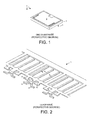
- FIG. 1 is a perspective diagram of a Direct-Bonded Copper (“DBC”) substrate.
- DBC Direct-Bonded Copper
- FIG. 2 is a perspective diagram of a leadframe.
- FIG. 3 is a cross-sectional showing the leadframe of FIG. 2 and the DBC substrate of FIG. 1 at the beginning of a package assembly process.
- FIG. 4 is a cross-sectional diagram showing the leadframe and the DBC substrate at a subsequent time in the package assembly process.
- FIG. 5 is a cross-sectional diagram that shows a contact pad and the DBC substrate both immediately before ultrasonic welding and immediately after ultrasonic welding.
- FIG. 6 is a cross-sectional diagram that shows a copper lift off problem associated with a previous nonpublic and non-commercial attempt to ultrasonically weld a DBC substrate to a leadframe.
- FIG. 7 is a cross-sectional diagram that shows an alumina cracking problem associated with the previous nonpublic and non-commercial attempt to ultrasonically weld a DBC substrate to a leadframe.
- FIG. 8 is a table that sets forth parameters of a ultrasonic welding process used to attach DBC substrates to leadframe contact pads in accordance with one novel aspect.
- FIG. 9 is a perspective view of a finished TO-247 packaged discrete power integrated circuit device, where the DBC substrate within the package is ultrasonically welded to contact pads of the center lead (the plastic encapsulant overmolding is not shown).
- FIG. 10 is a diagram of the bottom of the device of FIG. 9 showing the DBC substrate and the bent down extension portion of the center lead (the encapsulant, the emitter and base leads, and the associated bond wires are not shown).
- FIG. 11 is a simplified perspective diagram of a finished TO-247 device, where the DBC substrate is attached to the contact pads of the center lead with a solderless weld in accordance with one novel aspect.
- the first, second and third leads extend parallel to one another from the amount of encapsulant 34.
- FIG. 12 is a flowchart of a method in accordance with one novel aspect.
- FIG. 13 is a cross-sectional diagram of a second way that a DBC substrate can be connected to contact pads with a solderless weld.
- FIG. 14 is a perspective view of a finished TO-247 packaged power integrated circuit device, where the DBC substrate is laser welded to the contact pads of the center lead (the plastic encapsulant overmolding is not shown).
- FIG. 15 is a table that sets forth parameters of the laser welding process used to laser weld the DBC substrate to the contact pads in the structure of FIG. 14 .
- first object when a first object is referred to as being disposed “over” or “on” a second object, it is to be understood that the first object can be directly on the second object, or an intervening object may be present between the first and second objects.
- terms such as “front”, “back”, “upper”, “lower”, “top”, “bottom”, “underneath”, “underlying” and “down” are used herein to describe relative orientations between different parts of the structure being described, and it is to be understood that the overall structure being described can actually be oriented in any way in three-dimensional space.
- FIG. 1 is a perspective diagram of a Direct-Bonded Copper ("DBC") substrate 1.
- DBC substrate 1 involves a substrate layer 2 of an insulative material. Substrate layer 2 is sandwiched between a first (die-side) layer 3 of metal and a second (back-side) layer 4 of metal. The second back-side metal layer 4 is not seen in the perspective view of FIG. 1 because it is located underneath the structure pictured. Arrow 4 indicates that this second back-side metal layer 4 is disposed on the bottom side of the substrate layer 2 in the perspective shown.
- DBC substrate 1 involves a substrate layer 2 of an insulative material. Substrate layer 2 is sandwiched between a first (die-side) layer 3 of metal and a second (back-side) layer 4 of metal. The second back-side metal layer 4 is not seen in the perspective view of FIG. 1 because it is located underneath the structure pictured. Arrow 4 indicates that this second back-side metal layer 4 is disposed on the bottom side of the substrate layer 2 in the perspective shown.
- substrate layer 2 is a layer of an insulative material such as an insulative ceramic.
- the insulative ceramic is alumina (Al 2 O 3 ) that is 0.630 mm thick.
- first die-side metal layer 3 is a layer of copper plated and a plating of a thin upper layer of nickel.
- Metal layer 3 is at least 0.25 mm thick (for example, 0.30 mm thick).
- the nickel plating (optional) is 10 micrometers thick.
- Metal layer 3 may be referred to as a die-attach pad.
- second back-side metal layer 4 is a layer of copper and a plating of a thin upper layer of nickel. Layer 4 is at least 0.25 mm thick (for example, 0.30 mm thick).
- the nickel plating (optional) is 10 micrometers thick.
- DBC substrate 1 is made by placing a first sheet of metal on top of the sheet of alumina, and placing a second sheet of metal under the sheet of alumina. The three sheets are then pressed together in a high temperature furnace such that the metal sheets are mechanically pressed and melted down and fixed to the top and bottom surfaces of the alumina. The outer surfaces of the metal layers take on the somewhat irregular non-planar surfaces of the alumina layer. Irregularities of the alumina transfer through the metal layer sheets. After pressing, the metal sheets are patterned and etched using standard lithographic and etching processes. The resulting etched structure is then sectioned into smaller rectangular pieces. FIG. 1 shows one of these rectangular pieces.
- the outer edges of the first die-side metal layer are set back from the outer edges of substrate layer 2 so that a later-applied encapsulant will better cover the side edges of the die-side metal layer.
- the width of substrate layer 2 is about 14.2 mm and the length of layer substrate 2 is about 17.0 mm.
- FIG. 2 is a perspective diagram of a leadframe 5.
- Leadframe 5 is stamped from a single sheet of thick copper. The copper of the sheet is nickel plated. In another example, bare copper is used.
- a center portion of leadframe 5 involves a first lead portion 6, a second lead portion 7, and a third lead portion 8. Extending from the first lead portion 6 is a bent down extension portion 10 that terminates in two opposing finger-like contact pads 11 and 12. Extending from second lead portion 7 is a bonding extension portion 9. Extending from third lead portion 8 is a bonding extension portion 13.
- FIG. 3 is a cross-sectional diagram showing leadframe 5 and DBC substrate 1 at the beginning of a package assembly process.
- FIG. 4 is a cross-sectional diagram showing leadframe 5 and DBC substrate 1 at a subsequent time in the package assembly process.
- the leadframe and the DBC substrate are brought together as illustrated so that each pair of leadframe contact pads makes contact with a corresponding DBC substrate.
- Each leadframe contact pad is then attached with a solderless weld to a corresponding portion of the first die-side layer of the associated DBC substrate.
- the solderless weld is an ultrasonic weld.
- Sinusoidal waveform 44 is a representation of the relative ultrasonic movement that causes the welding to occur.
- FIG. 5 is a cross-sectional diagram that shows contact pad 12 and the edge of first die-side metal layer 3 in further detail both immediately before ultrasonic welding and immediately after ultrasonic welding.
- contact pad 12 is pressed down into and past the upper surface 45 of first die-side layer 3 by approximately 0.05 millimeters.
- an amount of metal 14 may pile up at the side edge 15 of contact pad 12 as pictured in the right portion of FIG. 5 .
- the weld is a solderless weld.
- FIG. 8 is a table that sets forth parameters of the ultrasonic welding process used to attach DBC substrates to leadframe contact pads in accordance with one novel aspect.
- each ultrasonic weld is carried out using 20kHz ultrasonic vibrations, having a peak-to-peak vibration amplitude of less than or equal to approximately 20 micrometers, for 0.25 seconds, under a welding pressure of not more than 0.05 Mpa.
- the parameters of FIG. 8 are used in the ultrasonic welding process, little or none of the lift off and cracking illustrated in FIG. 6 and FIG. 7 are seen to occur.
- a single power integrated circuit die is attached to the die-side metal layer of each DBC substrate.
- the single power integrated circuit die may, for example, be a power rectifier die, a power regulator die, a silicon controlled rectifier die, a power bipolar transistor integrated circuit die, a power insulated gate bipolar transistor circuit die, or a power field effect transistor integrated circuit die.
- bond pads on the top surfaces of the integrated circuit dice are wire bonded in conventional fashion to the corresponding wire bond portions of the corresponding leads of the leadframe.
- each die is overmolded with an amount of plastic encapsulant in conventional fashion.
- the back-side metal layer of each DBC substrate is, however, left at least partially exposed and is not entirely overmolded.
- conventional lead trimming is performed to cut individual TO-247 packaged devices from the leadframe. The wirebonding, the overmolding with encapsulant, and the trimming of interconnection portions of the leadframe to make the individual packaged devices are processes known in the art.
- FIG. 9 is a perspective view of one such finished TO-247 packaged device 22 with its plastic encapsulant overmolding not shown.
- the upper surfaces of contact pads 11 and 12 have nonplanar waffle-like indentations and contours 23.
- the indentations may be of the shape of intersecting rows and columns of V-shaped trenches.
- These indentations and contours 23 are a result of the force applied by an ultrasonic welding head.
- teeth or ridges on the bottom of the ultrasonic head cut down into the upper surface of the contact pads, thereby leaving the waffle-like indentations that correspond to the shape of the teeth or ridges.
- the type of marks left need not be waffle-like indentations rather may be nonplanar structures of another shape depending on the structure of the gripping bottom surface of the ultrasonic head.
- One and only one power semiconductor integrated circuit die 24 is die-attached to the first die-side metal layer 3 of DBC substrate 1.
- integrated circuit 24 is a discrete power bipolar transistor integrated circuit die.
- the bottom side of die 24 is the collector electrode 25.
- Collector electrode 25 is electrically and mechanically connected to the upper surface of the first die-side metal layer 3, and through this layer of metal and through contact pads 11 and 12, and bent down extension portion 10, to the center lead 6 of the TO-247 packaged device 22.
- An emitter contact pad 26 on the upper surface of die 24 is electrically coupled via multiple aluminum bond wires 27-29 to the lead extension portion 9 of packaged device 22.
- a base contact pad 30 on the upper surface of die 24 is electrically coupled via bond wire 31 to lead extension portion 13 of packaged device 22.
- the emitter and base leads 7 and 8 are held in place in the positions illustrated in FIG. 9 by the plastic encapsulant.
- the locations of the ultrasonic welds at the interfaces between the bottom of contact pads 11 and 12 and the top surface of die-side metal layer 3 are roughly identified by arrows 32 and 33.
- FIG. 10 is a diagram of the bottom of the device of FIG. 9 , showing the DBC substrate 1 and bent down extension portion 10 of the center lead.
- the encapsulant, the emitter and base leads, and the associated bond wires, are not shown in the simplified diagram of FIG. 10 .
- FIG. 11 is a simplified perspective diagram of the finished TO-247 device 22.
- the amount of plastic encapsulant 34 is shown.
- This encapsulant 34 covers the die 24, the bond wires 27-29 and 31, and the upper die-side metal layer 3 of the DBC substrate 1.
- the back-side metal layer 4 of DBC substrate 1 is not covered with encapsulant, but rather is exposed and forms the backside of the packaged device 22.
- This back-side metal layer 4 is not shown in FIG. 11 because it is the bottom side of the device pictured in the FIG. 11 .
- FIG. 12 is a flowchart of a method 100 in accordance with one novel aspect.
- a first metal layer of a DBC substrate is attached to at least one lead with a solderless weld, thereby forming an assembly (step 101).
- the solderless weld may be an ultrasonic weld.
- the solderless weld may be a laser weld.
- a first of the leads is a lead involving contact pads 11 and 12, bent portion 10, and lead portion 7; a second of the leads is a lead involving portion 9 and lead portion 6; and a third of the leads is a lead involving portion 13 and lead portion 8.
- one and only one power semiconductor integrated circuit is attached to the first metal layer of the assembly.
- the resulting DBC substrate and lead assembly is then incorporated (step 103) into a packaged power integrated circuit device.
- this incorporation involves wire bonding the die to the second and third leads, involves encapsulating the die and DBC/lead assembly, and involves lead trimming to form the resulting packaged power integrated circuit device.
- the resulting packaged power integrated circuit device conforms to the TO-247 outline and is the package 22 of FIG. 11 .
- FIG. 13 is a diagram of a second way that DBC substrate 1 can be connected to contact pads 11 and 12 with a solderless weld.
- laser light source device 35 and laser light 36 are used to laser weld contact pads 11 and 12 to the die-side metal layer 3 of DBC substrate 1.
- Laser light 36 provides localized heating to carry out the weld.
- the term "laser” is used here loosely. Energy from a high energy light source (whether laser light or another type of light) is used to heat small localized portions of contact pads 11 and 12 and thereby to weld the contact pads to the underlying metal layer 3. In one example, there is no intervening solder disposed between the contact pads 11 and 12 and the underlying metal layer 3.
- the weld is a solderless weld.
- FIG. 14 is a perspective view of a finished packed integrated circuit device 37 without its amount of encapsulant overmolding.
- the structure 37 of FIG. 14 is similar to the structure of FIG. 9 , except that in the case of the structure 37 of FIG. 14 the contact pads 11 and 12 have been laser welded to DBC substrate 1.
- the upper surface of each of contact pads 11 and 12 is has a row of five mound-shaped protrusions and corresponding pits.
- Reference numeral 38 identifies the right most such mound-shaped protrusion and pit structure on the top surface of contact pad 12.
- Each mound and pit structure is formed as a result of application of pulses of laser energy.
- the pulses of laser energy locally heat part of a contact pad to a molten state and cause it to fuse to a part of the upper surface of die-side metal layer 3 of the DBC substrate.
- the locations of the laser welds at the interfaces between the bottom of contact pads 11 and 12 and the top surface of die-side metal layer 3 are roughly identified by arrows 39 and 40.
- FIG. 15 is a table that sets forth parameters of the laser welding process used to weld the DBC substrate 1 of FIG. 14 to the contact pads 11 and 12 of FIG. 14 to make the packaged device of FIG. 14 .
- the packaged semiconductor device, the DBC substrate of the packaged semiconductor device, and the leads of the packaged semiconductor device are as described in U.S. Patent No. 6,404,065 .
- the packaged semiconductor device may conform to a package outline, such as the TO-220 outline, the TO-264 outline, or the SOT-227B outline.
- a package outline such as the TO-220 outline, the TO-264 outline, or the SOT-227B outline.
Landscapes
- Lead Frames For Integrated Circuits (AREA)
- Chemical & Material Sciences (AREA)
- Engineering & Computer Science (AREA)
- Ceramic Engineering (AREA)
Priority Applications (2)
| Application Number | Priority Date | Filing Date | Title |
|---|---|---|---|
| EP21195812.9A EP3940770B1 (fr) | 2012-01-05 | 2013-01-03 | Boîtier de transistor de puissance discret à fixer à un cadre de montage dbc sans soudure |
| EP19173863.2A EP3544053B1 (fr) | 2012-01-05 | 2013-01-03 | Boîtier de transistor de puissance discret à fixer à un cadre de montage dbc sans soudure |
Applications Claiming Priority (1)
| Application Number | Priority Date | Filing Date | Title |
|---|---|---|---|
| US13/344,567 US20130175704A1 (en) | 2012-01-05 | 2012-01-05 | Discrete power transistor package having solderless dbc to leadframe attach |
Related Child Applications (2)
| Application Number | Title | Priority Date | Filing Date |
|---|---|---|---|
| EP19173863.2A Division EP3544053B1 (fr) | 2012-01-05 | 2013-01-03 | Boîtier de transistor de puissance discret à fixer à un cadre de montage dbc sans soudure |
| EP21195812.9A Division EP3940770B1 (fr) | 2012-01-05 | 2013-01-03 | Boîtier de transistor de puissance discret à fixer à un cadre de montage dbc sans soudure |
Publications (2)
| Publication Number | Publication Date |
|---|---|
| EP2613352A2 true EP2613352A2 (fr) | 2013-07-10 |
| EP2613352A3 EP2613352A3 (fr) | 2015-12-23 |
Family
ID=47471635
Family Applications (3)
| Application Number | Title | Priority Date | Filing Date |
|---|---|---|---|
| EP13150118.1A Withdrawn EP2613352A3 (fr) | 2012-01-05 | 2013-01-03 | Boîtier de transistor de puissance discret à fixer à un cadre de montage dbc sans soudure |
| EP21195812.9A Active EP3940770B1 (fr) | 2012-01-05 | 2013-01-03 | Boîtier de transistor de puissance discret à fixer à un cadre de montage dbc sans soudure |
| EP19173863.2A Active EP3544053B1 (fr) | 2012-01-05 | 2013-01-03 | Boîtier de transistor de puissance discret à fixer à un cadre de montage dbc sans soudure |
Family Applications After (2)
| Application Number | Title | Priority Date | Filing Date |
|---|---|---|---|
| EP21195812.9A Active EP3940770B1 (fr) | 2012-01-05 | 2013-01-03 | Boîtier de transistor de puissance discret à fixer à un cadre de montage dbc sans soudure |
| EP19173863.2A Active EP3544053B1 (fr) | 2012-01-05 | 2013-01-03 | Boîtier de transistor de puissance discret à fixer à un cadre de montage dbc sans soudure |
Country Status (2)
| Country | Link |
|---|---|
| US (4) | US20130175704A1 (fr) |
| EP (3) | EP2613352A3 (fr) |
Cited By (3)
| Publication number | Priority date | Publication date | Assignee | Title |
|---|---|---|---|---|
| DE102013220591A1 (de) | 2013-10-11 | 2015-04-16 | Robert Bosch Gmbh | Leistungsmodul mit Kühlkörper |
| EP4372813A1 (fr) * | 2022-11-17 | 2024-05-22 | Infineon Technologies AG | Connecteur électrique à méandres et ouverture |
| US12218029B2 (en) | 2021-05-26 | 2025-02-04 | Infineon Technologies Austria Ag | Semiconductor device with improved performance in operation and improved flexibility in the arrangement of power chips |
Families Citing this family (30)
| Publication number | Priority date | Publication date | Assignee | Title |
|---|---|---|---|---|
| US20130175704A1 (en) * | 2012-01-05 | 2013-07-11 | Ixys Corporation | Discrete power transistor package having solderless dbc to leadframe attach |
| US9099391B2 (en) * | 2013-03-14 | 2015-08-04 | Infineon Technologies Austria Ag | Semiconductor package with top-side insulation layer |
| US10128174B2 (en) | 2015-07-24 | 2018-11-13 | Semiconductor Components Industries, Llc | Semiconductor component and method of manufacture |
| US9818674B2 (en) | 2015-07-24 | 2017-11-14 | Semiconductor Components Industries, Llc | Semiconductor component and method of manufacture |
| US9620443B2 (en) | 2015-07-24 | 2017-04-11 | Semiconductor Components Industries, Llc | Semiconductor component and method of manufacture |
| US9905500B2 (en) | 2015-07-24 | 2018-02-27 | Semiconductor Components Industries, Llc | Semiconductor component and method of manufacture |
| US9818677B2 (en) | 2015-07-24 | 2017-11-14 | Semiconductor Components Industries, Llc | Semiconductor component having group III nitride semiconductor device mounted on substrate and interconnected to lead frame |
| US9780019B2 (en) | 2015-07-24 | 2017-10-03 | Semiconductor Components Industries, Llc | Semiconductor component and method of manufacture |
| US9735095B2 (en) | 2015-07-24 | 2017-08-15 | Semiconductor Components Industries, Llc | Semiconductor component and method of manufacture |
| US10388539B2 (en) | 2015-07-24 | 2019-08-20 | Semiconductor Components Industries, Llc | Semiconductor component and method of manufacture |
| US9653387B2 (en) | 2015-07-24 | 2017-05-16 | Semiconductor Components Industries, Llc | Semiconductor component and method of manufacture |
| US9595950B1 (en) | 2016-05-31 | 2017-03-14 | Ixys Corporation | High-voltage stacked transistor circuit |
| JP6948855B2 (ja) * | 2017-06-30 | 2021-10-13 | 日立Astemo株式会社 | パワー半導体装置及びそれを用いた電力変換装置 |
| JP6819540B2 (ja) * | 2017-10-23 | 2021-01-27 | 三菱電機株式会社 | 半導体装置 |
| US10607931B2 (en) | 2018-07-03 | 2020-03-31 | Texas Instruments Incorporated | Semiconductor device with electroplated die attach |
| US10957635B2 (en) | 2019-03-20 | 2021-03-23 | Texas Instruments Incorporated | Multi-chip package with high thermal conductivity die attach |
| US10892209B2 (en) | 2019-03-25 | 2021-01-12 | Texas Instruments Incorporated | Semiconductor device with metal die attach to substrate with multi-size cavity |
| US10832991B1 (en) | 2019-05-07 | 2020-11-10 | Texas Instruments Incorporated | Leadless packaged device with metal die attach |
| US10832993B1 (en) | 2019-05-09 | 2020-11-10 | Texas Instruments Incorporated | Packaged multichip device with stacked die having a metal die attach |
| TWI752398B (zh) * | 2020-01-02 | 2022-01-11 | 財團法人工業技術研究院 | 功率模組 |
| IT202000023641A1 (it) * | 2020-10-07 | 2022-04-07 | St Microelectronics Srl | Elemento di bloccaggio dei piedini di connessione di piastrine semiconduttrici, in particolare per moduli di potenza per applicazioni automobilistiche, e metodo di assemblaggio |
| US11756882B2 (en) * | 2020-12-31 | 2023-09-12 | Texas Instruments Incorporated | Semiconductor die with blast shielding |
| US20220223488A1 (en) * | 2021-01-12 | 2022-07-14 | Texas Instruments Incorporated | Semiconductor packages including interface members for welding |
| KR102499825B1 (ko) * | 2021-02-05 | 2023-02-14 | 파워마스터반도체 주식회사 | 패키지형 전력 반도체 장치 |
| US20220310409A1 (en) | 2021-03-24 | 2022-09-29 | Littelfuse, Inc. | Method to connect power terminal to substrate within semiconductor package |
| CN114649217A (zh) * | 2022-03-17 | 2022-06-21 | 西安西奈电子科技股份有限公司 | 一种To-247低热阻高速绝缘封装方法 |
| CN115148723A (zh) * | 2022-07-06 | 2022-10-04 | 西安西奈电子科技有限公司 | 一种To-247外形的PFC(功率因数校正)模块封装方法 |
| DE102023206625A1 (de) * | 2022-08-01 | 2024-02-01 | Zf Friedrichshafen Ag | Leistungselektronikmodul |
| US12543611B2 (en) | 2023-04-19 | 2026-02-03 | Littelfuse, Inc. | Method to connect power terminal to substrate within semiconductor package |
| US20250132233A1 (en) * | 2023-10-18 | 2025-04-24 | Icp Technology Co., Ltd. | Heat-Electricity Discrete Power Module Including Two-Way Heat-Dissipation Ceramic Substrates and Manufacturing method of the Same |
Citations (3)
| Publication number | Priority date | Publication date | Assignee | Title |
|---|---|---|---|---|
| US4483810A (en) | 1982-02-06 | 1984-11-20 | Brown, Boveri And Cie Ag | Method for directly joining metal pieces to oxide-ceramic substrates |
| US6404065B1 (en) | 1998-07-31 | 2002-06-11 | I-Xys Corporation | Electrically isolated power semiconductor package |
| US6727585B2 (en) | 2001-05-04 | 2004-04-27 | Ixys Corporation | Power device with a plastic molded package and direct bonded substrate |
Family Cites Families (52)
| Publication number | Priority date | Publication date | Assignee | Title |
|---|---|---|---|---|
| US3051027A (en) * | 1959-11-16 | 1962-08-28 | Cavitron Ultrasonics Inc | Ultrasonic welding |
| US4546374A (en) * | 1981-03-23 | 1985-10-08 | Motorola Inc. | Semiconductor device including plateless package |
| US4631805A (en) * | 1981-03-23 | 1986-12-30 | Motorola Inc. | Semiconductor device including plateless package fabrication method |
| US5209390A (en) * | 1989-07-03 | 1993-05-11 | General Electric Company | Hermetic package and packaged semiconductor chip having closely spaced leads extending through the package lid |
| US5018002A (en) * | 1989-07-03 | 1991-05-21 | General Electric Company | High current hermetic package including an internal foil and having a lead extending through the package lid and a packaged semiconductor chip |
| JP3053298B2 (ja) * | 1992-08-19 | 2000-06-19 | 株式会社東芝 | 半導体装置 |
| US5971251A (en) * | 1997-10-27 | 1999-10-26 | Lear Automotive Dearborn, Inc. | Method of welding a terminal to a flat flexible cable |
| US6040626A (en) * | 1998-09-25 | 2000-03-21 | International Rectifier Corp. | Semiconductor package |
| JP2001127246A (ja) * | 1999-10-29 | 2001-05-11 | Fujitsu Ltd | 半導体装置 |
| DE10026743C1 (de) * | 2000-05-30 | 2002-01-03 | Eupec Gmbh & Co Kg | Substrat zur Aufnahme einer Schaltungsanordnung |
| JP2002009190A (ja) * | 2000-06-16 | 2002-01-11 | Ngk Spark Plug Co Ltd | セラミック基板及びその製造方法 |
| JP4422391B2 (ja) * | 2002-08-07 | 2010-02-24 | 矢崎総業株式会社 | 電線と端子の接続方法 |
| US6909589B2 (en) * | 2002-11-20 | 2005-06-21 | Corporation For National Research Initiatives | MEMS-based variable capacitor |
| US20060208033A1 (en) * | 2005-03-21 | 2006-09-21 | Welter Curtis L | Apparatus and method for connecting coated wires |
| JP2006278913A (ja) * | 2005-03-30 | 2006-10-12 | Toyota Motor Corp | 回路装置とその製造方法 |
| US7745930B2 (en) * | 2005-04-25 | 2010-06-29 | International Rectifier Corporation | Semiconductor device packages with substrates for redistributing semiconductor device electrodes |
| US20070130759A1 (en) * | 2005-06-15 | 2007-06-14 | Gem Services, Inc. | Semiconductor device package leadframe formed from multiple metal layers |
| US7511371B2 (en) * | 2005-11-01 | 2009-03-31 | Sandisk Corporation | Multiple die integrated circuit package |
| JP2007335632A (ja) * | 2006-06-15 | 2007-12-27 | Toyota Industries Corp | 半導体装置 |
| DE102006050653A1 (de) * | 2006-10-24 | 2008-04-30 | Carl Zeiss Smt Ag | Verfahren und Vorrichtung zum stoffschlüssigen Verbinden eines optischen Elementes mit einer Fassung |
| DE102006056363B4 (de) * | 2006-11-29 | 2010-12-09 | Infineon Technologies Ag | Halbleitermodul mit mindestens zwei Substraten und Verfahren zur Herstellung eines Halbleitermoduls mit zwei Substraten |
| DE102007041136A1 (de) * | 2007-08-30 | 2009-03-05 | Osram Opto Semiconductors Gmbh | LED-Gehäuse |
| KR101505552B1 (ko) * | 2008-03-31 | 2015-03-24 | 페어차일드코리아반도체 주식회사 | 복합 반도체 패키지 및 그 제조방법 |
| US7847375B2 (en) * | 2008-08-05 | 2010-12-07 | Infineon Technologies Ag | Electronic device and method of manufacturing same |
| US8455987B1 (en) * | 2009-06-16 | 2013-06-04 | Ixys Corporation | Electrically isolated power semiconductor package with optimized layout |
| WO2011036307A1 (fr) * | 2009-09-28 | 2011-03-31 | Abb Technology Ag | Agencement de circuit et son procédé de fabrication |
| DE102009045181B4 (de) * | 2009-09-30 | 2020-07-09 | Infineon Technologies Ag | Leistungshalbleitermodul |
| US20110121326A1 (en) * | 2009-11-26 | 2011-05-26 | Dsem Holdings Sdn. Bhd. | Submount Having Reflective Cu-Ni-Ag Pads Formed Using Electroless Deposition |
| US8313622B2 (en) * | 2010-07-09 | 2012-11-20 | Rsr Technologies, Inc. | Electrochemical anodes having friction stir welded joints and methods of manufacturing such anodes |
| IT1404382B1 (it) * | 2011-02-24 | 2013-11-22 | St Microelectronics Srl | Dispositivo elettronico per applicazioni ad elevata potenza. |
| US9041183B2 (en) * | 2011-07-19 | 2015-05-26 | Ut-Battelle, Llc | Power module packaging with double sided planar interconnection and heat exchangers |
| US8563364B2 (en) * | 2011-09-29 | 2013-10-22 | Infineon Technologies Ag | Method for producing a power semiconductor arrangement |
| US20130175704A1 (en) * | 2012-01-05 | 2013-07-11 | Ixys Corporation | Discrete power transistor package having solderless dbc to leadframe attach |
| US8866274B2 (en) * | 2012-03-27 | 2014-10-21 | Infineon Technologies Ag | Semiconductor packages and methods of formation thereof |
| JP5387715B2 (ja) * | 2012-04-06 | 2014-01-15 | 住友電気工業株式会社 | 半導体デバイス |
| US8716864B2 (en) * | 2012-06-07 | 2014-05-06 | Ixys Corporation | Solderless die attach to a direct bonded aluminum substrate |
| JP5991045B2 (ja) * | 2012-06-28 | 2016-09-14 | 住友電気工業株式会社 | 半導体装置 |
| US8586480B1 (en) * | 2012-07-31 | 2013-11-19 | Ixys Corporation | Power MOSFET having selectively silvered pads for clip and bond wire attach |
| US8575767B1 (en) * | 2012-10-06 | 2013-11-05 | Ixys Corporation | Reflow of thermoplastic sheet for passivation of power integrated circuits |
| US9640460B2 (en) * | 2013-02-05 | 2017-05-02 | Panasonic Intellectual Property Management Co., Ltd. | Semiconductor device with a heat-dissipating plate |
| US9967977B1 (en) * | 2013-06-18 | 2018-05-08 | Cree Fayetteville, Inc. | Step etched metal electrical contacts |
| JP6413709B2 (ja) * | 2014-12-02 | 2018-10-31 | 富士電機株式会社 | 半導体装置およびその製造方法 |
| KR20170086828A (ko) * | 2016-01-19 | 2017-07-27 | 제엠제코(주) | 메탈범프를 이용한 클립 본딩 반도체 칩 패키지 |
| JP6665926B2 (ja) * | 2016-03-22 | 2020-03-13 | 富士電機株式会社 | 半導体装置および半導体装置の製造方法 |
| DE102016112289B4 (de) * | 2016-07-05 | 2020-07-30 | Danfoss Silicon Power Gmbh | Leiterrahmen und Verfahren zur Herstellung desselben |
| AT519175B1 (de) * | 2016-08-03 | 2019-01-15 | Gebauer & Griller Kabelwerke Ges M B H | Ultraschallverschweissen eines litzenleiters mit einem kontaktteil |
| KR101694657B1 (ko) * | 2016-08-04 | 2017-01-09 | 제엠제코(주) | 방열 구조를 갖는 반도체 패키지 |
| US9716057B1 (en) * | 2016-08-24 | 2017-07-25 | United Silicon Carbide, Inc. | Offset leadframe cascode package |
| CN109983574B (zh) * | 2016-11-23 | 2023-05-12 | 日立能源瑞士股份公司 | 功率半导体模块的制造 |
| DE102017108114B4 (de) * | 2017-04-13 | 2025-10-23 | Infineon Technologies Ag | Chipmodul mit räumlich eingeschränktem thermisch leitfähigen Montagekörper |
| US10629520B2 (en) * | 2017-05-29 | 2020-04-21 | Rohm Co., Ltd. | Semiconductor device and method for manufacturing the same |
| DE102018206482B4 (de) * | 2018-04-26 | 2024-01-25 | Infineon Technologies Ag | Halbleiterbauelement mit einem Verbundwerkstoffclip aus Verbundmaterial |
-
2012
- 2012-01-05 US US13/344,567 patent/US20130175704A1/en not_active Abandoned
-
2013
- 2013-01-03 EP EP13150118.1A patent/EP2613352A3/fr not_active Withdrawn
- 2013-01-03 EP EP21195812.9A patent/EP3940770B1/fr active Active
- 2013-01-03 EP EP19173863.2A patent/EP3544053B1/fr active Active
-
2017
- 2017-03-07 US US15/452,699 patent/US20170178998A1/en not_active Abandoned
-
2018
- 2018-11-02 US US16/179,432 patent/US10720376B2/en active Active
-
2020
- 2020-06-09 US US16/896,594 patent/US11387162B2/en active Active
Patent Citations (3)
| Publication number | Priority date | Publication date | Assignee | Title |
|---|---|---|---|---|
| US4483810A (en) | 1982-02-06 | 1984-11-20 | Brown, Boveri And Cie Ag | Method for directly joining metal pieces to oxide-ceramic substrates |
| US6404065B1 (en) | 1998-07-31 | 2002-06-11 | I-Xys Corporation | Electrically isolated power semiconductor package |
| US6727585B2 (en) | 2001-05-04 | 2004-04-27 | Ixys Corporation | Power device with a plastic molded package and direct bonded substrate |
Cited By (4)
| Publication number | Priority date | Publication date | Assignee | Title |
|---|---|---|---|---|
| DE102013220591A1 (de) | 2013-10-11 | 2015-04-16 | Robert Bosch Gmbh | Leistungsmodul mit Kühlkörper |
| US12218029B2 (en) | 2021-05-26 | 2025-02-04 | Infineon Technologies Austria Ag | Semiconductor device with improved performance in operation and improved flexibility in the arrangement of power chips |
| EP4372813A1 (fr) * | 2022-11-17 | 2024-05-22 | Infineon Technologies AG | Connecteur électrique à méandres et ouverture |
| US12519256B2 (en) | 2022-11-17 | 2026-01-06 | Infineon Technologies Ag | Electrical connector with meander and opening |
Also Published As
| Publication number | Publication date |
|---|---|
| US20130175704A1 (en) | 2013-07-11 |
| EP3544053A1 (fr) | 2019-09-25 |
| EP3940770A1 (fr) | 2022-01-19 |
| EP2613352A3 (fr) | 2015-12-23 |
| US20170178998A1 (en) | 2017-06-22 |
| EP3544053B1 (fr) | 2021-09-15 |
| US11387162B2 (en) | 2022-07-12 |
| US10720376B2 (en) | 2020-07-21 |
| EP3940770B1 (fr) | 2024-10-09 |
| US20190088571A1 (en) | 2019-03-21 |
| US20200303281A1 (en) | 2020-09-24 |
Similar Documents
| Publication | Publication Date | Title |
|---|---|---|
| US11387162B2 (en) | Discrete power transistor package having solderless DBC to leadframe attach | |
| JP4294405B2 (ja) | 半導体装置 | |
| JP5634033B2 (ja) | 樹脂封止型半導体装置とその製造方法 | |
| CN1331224C (zh) | 树脂封装型半导体装置 | |
| CN107615464B (zh) | 电力用半导体装置的制造方法以及电力用半导体装置 | |
| US8133759B2 (en) | Leadframe | |
| CN113097173B (zh) | 半导体封装及其制造方法 | |
| JP2013539919A (ja) | 半導体モジュールおよび半導体モジュールを製造する方法 | |
| US20120074516A1 (en) | Semiconductor device | |
| CN108242435B (zh) | 半导体器件的制造方法 | |
| JP2014513870A (ja) | ウォータフォール・ワイヤボンディング | |
| KR102173436B1 (ko) | 대면 장착 다이들을 구비하고 내부 본드와이어들을 구비하지 않는 얇은 프로파일 전력 반도체 장치 패키지 | |
| JP2008153432A (ja) | 半導体装置およびその製造方法 | |
| JP6091443B2 (ja) | 半導体モジュール | |
| JP5553766B2 (ja) | 半導体装置とその製造方法 | |
| CN114078716B (zh) | 半导体器件及其制造方法 | |
| JP2009123873A (ja) | 発光ダイオード封止構造およびその製造方法 | |
| CN102054658B (zh) | 封装打线工艺的加热治具及其方法 | |
| US20110163392A1 (en) | Semiconductor device and method of manufacturing the same | |
| JPH10178128A (ja) | 半導体装置、およびその製造方法 | |
| JPH0637221A (ja) | 樹脂封止型半導体装置 | |
| TW201810470A (zh) | 引線接合方法 | |
| JP2025147545A (ja) | 半導体装置および半導体装置の製造方法 | |
| JP2014011396A (ja) | 半導体装置の実装構造および半導体装置の実装方法 | |
| JP2000200867A (ja) | 半導体パッケ―ジ及びその組立方法 |
Legal Events
| Date | Code | Title | Description |
|---|---|---|---|
| PUAI | Public reference made under article 153(3) epc to a published international application that has entered the european phase |
Free format text: ORIGINAL CODE: 0009012 |
|
| AK | Designated contracting states |
Kind code of ref document: A2 Designated state(s): AL AT BE BG CH CY CZ DE DK EE ES FI FR GB GR HR HU IE IS IT LI LT LU LV MC MK MT NL NO PL PT RO RS SE SI SK SM TR |
|
| AX | Request for extension of the european patent |
Extension state: BA ME |
|
| PUAL | Search report despatched |
Free format text: ORIGINAL CODE: 0009013 |
|
| AK | Designated contracting states |
Kind code of ref document: A3 Designated state(s): AL AT BE BG CH CY CZ DE DK EE ES FI FR GB GR HR HU IE IS IT LI LT LU LV MC MK MT NL NO PL PT RO RS SE SI SK SM TR |
|
| AX | Request for extension of the european patent |
Extension state: BA ME |
|
| RIC1 | Information provided on ipc code assigned before grant |
Ipc: H01L 23/373 20060101AFI20151118BHEP Ipc: H01L 23/495 20060101ALI20151118BHEP Ipc: H01L 23/433 20060101ALI20151118BHEP |
|
| 17P | Request for examination filed |
Effective date: 20160616 |
|
| RBV | Designated contracting states (corrected) |
Designated state(s): AL AT BE BG CH CY CZ DE DK EE ES FI FR GB GR HR HU IE IS IT LI LT LU LV MC MK MT NL NO PL PT RO RS SE SI SK SM TR |
|
| STAA | Information on the status of an ep patent application or granted ep patent |
Free format text: STATUS: EXAMINATION IS IN PROGRESS |
|
| 17Q | First examination report despatched |
Effective date: 20161109 |
|
| GRAP | Despatch of communication of intention to grant a patent |
Free format text: ORIGINAL CODE: EPIDOSNIGR1 |
|
| STAA | Information on the status of an ep patent application or granted ep patent |
Free format text: STATUS: GRANT OF PATENT IS INTENDED |
|
| INTG | Intention to grant announced |
Effective date: 20190110 |
|
| STAA | Information on the status of an ep patent application or granted ep patent |
Free format text: STATUS: THE APPLICATION IS DEEMED TO BE WITHDRAWN |
|
| 18D | Application deemed to be withdrawn |
Effective date: 20190521 |