EP2621085A2 - Einstellbarer Leistungsteiler und entsprechende Verfahren und Vorrichtungen - Google Patents
Einstellbarer Leistungsteiler und entsprechende Verfahren und Vorrichtungen Download PDFInfo
- Publication number
- EP2621085A2 EP2621085A2 EP13151802.9A EP13151802A EP2621085A2 EP 2621085 A2 EP2621085 A2 EP 2621085A2 EP 13151802 A EP13151802 A EP 13151802A EP 2621085 A2 EP2621085 A2 EP 2621085A2
- Authority
- EP
- European Patent Office
- Prior art keywords
- adjustable
- power
- signal
- output
- phase
- Prior art date
- Legal status (The legal status is an assumption and is not a legal conclusion. Google has not performed a legal analysis and makes no representation as to the accuracy of the status listed.)
- Granted
Links
Images



Classifications
-
- H—ELECTRICITY
- H03—ELECTRONIC CIRCUITRY
- H03F—AMPLIFIERS
- H03F1/00—Details of amplifiers with only discharge tubes, only semiconductor devices or only unspecified devices as amplifying elements
- H03F1/02—Modifications of amplifiers to raise the efficiency, e.g. gliding Class A stages, use of an auxiliary oscillation
- H03F1/0205—Modifications of amplifiers to raise the efficiency, e.g. gliding Class A stages, use of an auxiliary oscillation in transistor amplifiers
- H03F1/0288—Modifications of amplifiers to raise the efficiency, e.g. gliding Class A stages, use of an auxiliary oscillation in transistor amplifiers using a main and one or several auxiliary peaking amplifiers whereby the load is connected to the main amplifier using an impedance inverter, e.g. Doherty amplifiers
-
- G—PHYSICS
- G06—COMPUTING OR CALCULATING; COUNTING
- G06F—ELECTRIC DIGITAL DATA PROCESSING
- G06F13/00—Interconnection of, or transfer of information or other signals between, memories, input/output devices or central processing units
- G06F13/38—Information transfer, e.g. on bus
- G06F13/42—Bus transfer protocol, e.g. handshake; Synchronisation
- G06F13/4282—Bus transfer protocol, e.g. handshake; Synchronisation on a serial bus, e.g. I2C bus, SPI bus
-
- G—PHYSICS
- G06—COMPUTING OR CALCULATING; COUNTING
- G06G—ANALOGUE COMPUTERS
- G06G7/00—Devices in which the computing operation is performed by varying electric or magnetic quantities
- G06G7/10—Power supply arrangements
-
- H—ELECTRICITY
- H03—ELECTRONIC CIRCUITRY
- H03F—AMPLIFIERS
- H03F1/00—Details of amplifiers with only discharge tubes, only semiconductor devices or only unspecified devices as amplifying elements
- H03F1/32—Modifications of amplifiers to reduce non-linear distortion
- H03F1/3241—Modifications of amplifiers to reduce non-linear distortion using predistortion circuits
- H03F1/3282—Acting on the phase and the amplitude of the input signal
-
- H—ELECTRICITY
- H03—ELECTRONIC CIRCUITRY
- H03F—AMPLIFIERS
- H03F3/00—Amplifiers with only discharge tubes or only semiconductor devices as amplifying elements
- H03F3/189—High-frequency amplifiers, e.g. radio frequency amplifiers
-
- H—ELECTRICITY
- H03—ELECTRONIC CIRCUITRY
- H03F—AMPLIFIERS
- H03F3/00—Amplifiers with only discharge tubes or only semiconductor devices as amplifying elements
- H03F3/189—High-frequency amplifiers, e.g. radio frequency amplifiers
- H03F3/19—High-frequency amplifiers, e.g. radio frequency amplifiers with semiconductor devices only
-
- H—ELECTRICITY
- H03—ELECTRONIC CIRCUITRY
- H03F—AMPLIFIERS
- H03F3/00—Amplifiers with only discharge tubes or only semiconductor devices as amplifying elements
- H03F3/20—Power amplifiers, e.g. Class B amplifiers, Class C amplifiers
- H03F3/21—Power amplifiers, e.g. Class B amplifiers, Class C amplifiers with semiconductor devices only
- H03F3/211—Power amplifiers, e.g. Class B amplifiers, Class C amplifiers with semiconductor devices only using a combination of several amplifiers
-
- H—ELECTRICITY
- H03—ELECTRONIC CIRCUITRY
- H03F—AMPLIFIERS
- H03F3/00—Amplifiers with only discharge tubes or only semiconductor devices as amplifying elements
- H03F3/60—Amplifiers in which coupling networks have distributed constants, e.g. with waveguide resonators
- H03F3/602—Combinations of several amplifiers
-
- H—ELECTRICITY
- H03—ELECTRONIC CIRCUITRY
- H03F—AMPLIFIERS
- H03F3/00—Amplifiers with only discharge tubes or only semiconductor devices as amplifying elements
- H03F3/68—Combinations of amplifiers, e.g. multi-channel amplifiers for stereophonics
-
- H—ELECTRICITY
- H03—ELECTRONIC CIRCUITRY
- H03G—CONTROL OF AMPLIFICATION
- H03G1/00—Details of arrangements for controlling amplification
- H03G1/0005—Circuits characterised by the type of controlling devices operated by a controlling current or voltage signal
- H03G1/0088—Circuits characterised by the type of controlling devices operated by a controlling current or voltage signal using discontinuously variable devices, e.g. switch-operated
-
- H—ELECTRICITY
- H04—ELECTRIC COMMUNICATION TECHNIQUE
- H04L—TRANSMISSION OF DIGITAL INFORMATION, e.g. TELEGRAPHIC COMMUNICATION
- H04L27/00—Modulated-carrier systems
- H04L27/18—Phase-modulated carrier systems, i.e. using phase-shift keying
- H04L27/22—Demodulator circuits; Receiver circuits
-
- H—ELECTRICITY
- H04—ELECTRIC COMMUNICATION TECHNIQUE
- H04L—TRANSMISSION OF DIGITAL INFORMATION, e.g. TELEGRAPHIC COMMUNICATION
- H04L7/00—Arrangements for synchronising receiver with transmitter
- H04L7/0079—Receiver details
-
- H—ELECTRICITY
- H03—ELECTRONIC CIRCUITRY
- H03F—AMPLIFIERS
- H03F2200/00—Indexing scheme relating to amplifiers
- H03F2200/387—A circuit being added at the output of an amplifier to adapt the output impedance of the amplifier
-
- H—ELECTRICITY
- H03—ELECTRONIC CIRCUITRY
- H03F—AMPLIFIERS
- H03F2200/00—Indexing scheme relating to amplifiers
- H03F2200/438—Separate feedback of amplitude and phase signals being present
-
- H—ELECTRICITY
- H03—ELECTRONIC CIRCUITRY
- H03F—AMPLIFIERS
- H03F2200/00—Indexing scheme relating to amplifiers
- H03F2200/451—Indexing scheme relating to amplifiers the amplifier being a radio frequency amplifier
-
- H—ELECTRICITY
- H03—ELECTRONIC CIRCUITRY
- H03F—AMPLIFIERS
- H03F2203/00—Indexing scheme relating to amplifiers with only discharge tubes or only semiconductor devices as amplifying elements covered by H03F3/00
- H03F2203/20—Indexing scheme relating to power amplifiers, e.g. Class B amplifiers, Class C amplifiers
- H03F2203/21—Indexing scheme relating to power amplifiers, e.g. Class B amplifiers, Class C amplifiers with semiconductor devices only
- H03F2203/211—Indexing scheme relating to power amplifiers, e.g. Class B amplifiers, Class C amplifiers with semiconductor devices only using a combination of several amplifiers
- H03F2203/21106—An input signal being distributed in parallel over the inputs of a plurality of power amplifiers
-
- H—ELECTRICITY
- H03—ELECTRONIC CIRCUITRY
- H03F—AMPLIFIERS
- H03F2203/00—Indexing scheme relating to amplifiers with only discharge tubes or only semiconductor devices as amplifying elements covered by H03F3/00
- H03F2203/20—Indexing scheme relating to power amplifiers, e.g. Class B amplifiers, Class C amplifiers
- H03F2203/21—Indexing scheme relating to power amplifiers, e.g. Class B amplifiers, Class C amplifiers with semiconductor devices only
- H03F2203/211—Indexing scheme relating to power amplifiers, e.g. Class B amplifiers, Class C amplifiers with semiconductor devices only using a combination of several amplifiers
- H03F2203/21193—Indexing scheme relating to power amplifiers, e.g. Class B amplifiers, Class C amplifiers with semiconductor devices only using a combination of several amplifiers the supply voltage of a power amplifier being continuously controlled, e.g. by an active potentiometer
-
- H—ELECTRICITY
- H03—ELECTRONIC CIRCUITRY
- H03G—CONTROL OF AMPLIFICATION
- H03G2201/00—Indexing scheme relating to subclass H03G
- H03G2201/10—Gain control characterised by the type of controlled element
- H03G2201/106—Gain control characterised by the type of controlled element being attenuating element
Definitions
- This invention relates to power or signal splitters in general and more specifically to techniques and apparatus for adjustable power or signal splitting or dividing.
- Power splitters or signal splitters or dividers are known. They are used, as the name suggests, to divide or split a signal into two or more identical signals. Identical or nearly identical signals can be used in various systems where the same signal is processed in varying manners or the same manner with more than one resultant signal being used in some combination for some purpose. For example, if signals are subject to the same interferences or distortions a practitioner can start with identical signals and use differential processing and subtract the resultant signals to basically eliminate the common interferences. As another example, some amplifiers use or start with identical signals and process these signals in distinctly different manners and then combine the resultant signals in some fashion to provide the final amplified signal.
- FIG. 1 depicts in a simplified and representative form an adjustable power splitter being used in a Doherty power amplifier system in accordance with one or more embodiments;
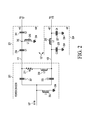
- FIG. 2 in a representative form, shows a diagram of a power divider and fixed phase shifter in accordance with one or more embodiments, which is suitable for use in the FIG. 1 adjustable power splitter;
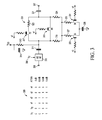
- FIG. 3 depicts a representative diagram of an adjustable attenuator in accordance with one or more embodiments
- FIG. 4 depicts a representative diagram of an adjustable phase shifter in accordance with one or more embodiments
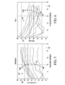
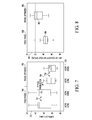
- FIG. 5 - 8 show various performance data of one or more embodiments.
- FIG. 9 shows a flow chart of a method of adjusting a power split signal that may be used in conjunction with the FIG. 1 system in accordance with one or more embodiments.
- Embodiments of the present disclosure concern adjustable power splitters and methods therein and uses thereof, e.g., adjustable radio frequency power splitters, and more specifically techniques and apparatus for independently adjusting the signals at each output of the adjustable power splitter so the adjustable power splitter is or can be arranged and constructed for use with a Doherty power amplifier. More particularly various inventive concepts and principles embodied in methods and apparatus corresponding to adjustable power splitters suitable for use in amplifiers or Doherty amplifiers for improved efficiency, etc. will be discussed and disclosed.
- an adjustable power splitter 101 or radio frequency power splitter is coupled to or being utilized with or driving an amplifier, specifically a Doherty amplifier or Doherty power amplifier 103.
- the adjustable power splitter 101 includes a power divider 105 with an input 107 and a first and second divider output 109, 111.
- the power divider 105 operates to divide or split a signal at the input 107 into two (or more in other embodiments - not specifically shown) signals, which are identical or very nearly identical signals with in some embodiments equal power.
- This equal power form of power divider is often referred to as a 3 dB divider since the resultant signals are each 3 dB less than the signal at the input. While the 3 dB divider is typical, other dividers with multiple outputs or outputs with unequal signals could be fashioned and used in some applications.
- One or more embodiments of the power divider can be a lumped element circuit including an inductive and a capacitive reactance as will be further discussed below with reference to FIG. 2
- adjustable power splitter 101 which in some embodiments is an adjustable radio frequency power splitter as shown in FIG. 1 , is a first adjustable phase shifter 113 and in some embodiments a first adjustable attenuator 115, which are series coupled to the first divider output 109 and configured for providing a first power output 117.
- the adjustable phase shifter and adjustable attenuator can be series coupled to each other in any order, i.e., attenuator followed by phase shifter as shown or vice versa.
- second adjustable phase shifter 119 and in some embodiments a second adjustable attenuator 121 which are series coupled to the second divider output 111 and configured for providing a second power output 123. As noted above, the order in which these are series coupled to each other can be changed.
- the first and typically the second adjustable phase shifter 113, 119 are each digitally controlled, e.g., by controller 125 and have a plurality of states.
- the first adjustable phase shifter 113 and often the second adjustable phase shifter 119 each have eight phase shifted states with each state providing a different amount of phase shift. It will be appreciated that the first and second phase shifter may have different phase shifted states, cover different ranges, and have different steps sizes, although typically they will be essentially the same.
- the adjustable phase shifters in many embodiments are analog phase shifters.
- the analog phase shifters while analog are controlled to provide a number of discrete phase shifts, i.e., digitally controlled,
- One or more embodiments of the adjustable phase shifters 113, 119 will be discussed below with reference to FIG. 4 .
- the first and typically the second adjustable attenuator 115, 121 are each digitally controlled (one or more control signals change between discrete steps or states and thus change between certain values of attenuation), e.g., by controller 125 and have a plurality of states.
- the first adjustable attenuator 115 and often the second adjustable attenuator 121 each have eight attenuation states or attenuation levels. It will be appreciated that the first and second attenuation may have different attenuation states, cover different attenuation ranges, and have different attenuation steps sizes, although typically they will be essentially the same.
- the adjustable attenuators in many embodiments are analog attenuators. One or more embodiments of the adjustable attenuators 115, 121 will be discussed below with reference to FIG. 3 .
- the adjustable power splitter 101 further include a fixed phase shifter 127 that is configured for adding a fixed phase shift between first and second signals at the, respective, first and second power outputs 117, 123.
- this can be a fixed and predetermined phase shift, e.g., 90 degrees, added to one signal path, i.e., path between output 109 and power output 117 or path between output 111 and power output 123.
- a ninety degree phase shift is added to one path in the amplifier and the fixed phase shift can be used to offset this amplifier phase shift.
- the fixed phase shift in some embodiments is a phase shift in a direction (negative or positive), e.g., a negative shift ⁇ /8 129, such as a negative forty five degree shift, for the first signal at the first power output 117 and a phase shift in the opposite direction, e.g., a positive shift ⁇ /8 131 such as a positive forty five degree phase shift for the second signal at the second power output 123.
- a phase shifter 127 or negative shift 129 and positive shift 131 can be lumped element circuits having an inductive and a capacitive reactance as will be further discussed below with reference to FIG. 2 .
- the adjustable power splitter 101 typically further comprises the controller 125, which is configured and arranged to control or for controlling the adjustable phase shifters and adjustable attenuators.
- the controller 125 in varying embodiments can be a processor or control circuitry or simply a one time programmable latch.
- the controller 125 can be provided data via an interface 133, such as a serial interface and in some embodiments this a serial peripheral interface (SPI), which as is known typically includes a data in and out, clock signal, and chip select lines.
- SPI serial peripheral interface
- control of the attenuators or phase shifters amounts to controlling switches, typically solid state or integrated switches such as some form of field effect transistor switch.
- the controller can be provided state information for all switches in all attenuators and phase shifters and essentially act as one or more latching buffers with outputs arranged and coupled to insure that all switches are in the appropriate ON or OFF state. In some embodiments this can be as simple as fuses at each gate, which are set to insure that all gates stay in a specified or desired state. Alternatively, the controller can be provided in essence an address or two or more addresses, which address(es) uniquely specify a state for each attenuator and phase shifter.
- phase shifters and attenuators are 8 state devices a 3 bit address for each would uniquely specify the proper state and 4 such addresses could be provided to the controller, which would convert each address to the appropriate control signals for each attenuator and phase shifter and latch in these values, etc.
- the amount of phase shift and attenuation for each of the four devices could be sent to the controller and it could determine the proper state to realize the desired shifts and attenuations. The practitioner is free to choose from among these or other approaches or combinations to make and retain the appropriate adjustments to the adjustable attenuators and adjustable phase shifters.
- the radio frequency Doherty power amplifier 103 is shown where this amplifier includes a main amplifier 135 coupled via a matching network or circuit 137 to the first power output 117 and a peaking amplifier 139 coupled by its matching circuit 141 to the second power output 123.
- the main and peaking amplifiers are comprised of one or more stages of low level amplification and higher power level amplification.
- the main and peaking amplifiers are coupled via, respective, output matching circuits 143, 145 to a Doherty combiner 147, which as is known is configured such that the main amplifier provides the amplification for lower level signals and both amplifiers combine to provide the amplification for high level signals.
- Adjustments to the adjustable attenuators and adjustable phase shifters can be made in an experimental manner by monitoring power drawn by the peaking stage or main stage or both as a function of signal levels and the like. At certain signal levels the peaking amplifier should begin to operate and amplitude and phase adjustments can be made with this in mind.
- FIG. 1 illustrates additional features for the adjustable power splitter with a Doherty amplifier where these features have been discussed above or will be discussed below in further detail.
- the first and second adjustable phase shifters and the first and second adjustable attenuators are digitally controlled with each having multiple states, e.g., 8 or more or less states.
- the power divider can be a lumped element circuit including one or more inductive reactance and capacitive reactance and other elements.
- the lumped element circuit can further include a first lumped element phase shifter configured to provide a negative forty five degree phase shift for a first signal at the first power output and a second lumped element phase shifter configured to provide a positive forty five degree phase shift for a second signal at the second power output.
- the adjustable power splitter with Doherty amplifier can also include or comprise a controller for controlling the adjustable phase shifters and adjustable attenuators.
- FIG. 2 a representative diagram of a power divider and fixed phase shifter(s) in accordance with one or more embodiments, which embodiments are suitable for use in the FIG. 1 adjustable power splitter, will be briefly discussed and described.
- like reference numbers will designate like features from other FIGs.
- FIG. 2 illustrates an input or RF input 107 to a power divider 201 which has a first output or divider output 109 and a second output or divider output 111 (I/O numbered same as FIG.1 ).
- the power divider as illustrated is implemented with one or more inductive reactances 203, 209, e.g., lumped element or discrete element inductances, and one or more capacitive reactances 205, 207, e.g., lumped element or discrete element capacitances, as well as a resistive loss or resistor 211.
- Lumped or discrete element is used herein to distinguish, for example, between structures whose purpose, structure, and properties are for providing a reactance as opposed to structures with a distributed structure, such as strip line or micro strip line based transmission lines, which can under some circumstances display properties that include or are similar to an inductive or capacitive reactance.
- a shunt inductance 203 or inductor is coupled from the input to a reference node (ground) 204.
- This inductance will operate to reduce power in any low frequency signals at the input.
- Two series capacitances 205, 207 or capacitors 205, 207 are coupled from the input to, respectively, the first divider output 109 and the second divider output 111. These capacitances will typically be equal valued for a 3 dB splitter.
- a series coupled inductance 209 and resistance 211 is coupled between the first and second divider outputs and operates to balance the signal at these outputs. The actual values for the inductors and capacitors and resistor will vary in accordance with operating frequencies and operating impedances.
- the shunt inductor 203 in combination with capacitor 207 forms a high pass structure which exhibits an impedance transformation between 107 (100 ohms for example) to 111 (50 ohms for example).
- inductor 203 in combination with capacitor 205 forms a high pass structure which exhibits an impedance transformation between 107 (100 ohms for example) to 109 (50 ohms for example).
- Resistor 211 in combination with inductor 209 creates a 50 ohm (nominal) odd-mode impedance at nodes 111 and 109.
- the combination of the elements is such that nodes 107, 109, and 111 each exhibit an impedance of 50 ohms (for example) and the combination of elements can be further chosen such that an equal or unequal power is split from 107 to 111 and 107 to 109, respectively.
- An alternative embodiment for the power splitter could use transmission lines although it is noted that these embodiments may not be as useful (e.g., much larger in physical size) over as broad of a bandwidth as the lumped element embodiments.
- FIG. 2 also illustrates an embodiment of the fixed phase shifter in accordance with fixed phase shifter 127 and more specifically two fixed, but opposite direction phase shifters.
- One is a negative shift 229 such as a negative forty five degree shift that is coupled to divider output 109 and provides an output that goes to adjustable attenuator 115 (see FIG. 1 ).
- This negative shift 229 corresponds to negative shift 129 of FIG. 1 .
- the negative shift 229 is a lumped element circuit having or implemented with an inductive reactance 233 coupled from divider output 109 to adjustable attenuator 115 and further having an input capacitive reactance 235 coupled from divider output 109 to a reference node (ground) 204 and an output capacitive reactance 237 or capacitor coupled from adjustable attenuator 115 input to the reference node 204.
- the specific values for the inductors and capacitors will depend on operating impedances and signal frequencies but can be experimentally determined by practitioners without undue experimentation.
- the other fixed shift is a positive shift 231, such as a positive forty five degree shift that is coupled to divider output 111 and provides an output that goes to adjustable attenuator 121 (see FIG. 1 ).
- the positive shift 231 corresponds to the positive shift 131 of FIG. 1 .
- the positive shift 231 is a lumped element circuit having an input capacitive reactance 239 coupled from divider output 111 to a common node 240 and an output capacitive reactance 241 or capacitor coupled from the common node 240 to adjustable attenuator 121 input. Further included is an inductive reactance 233 coupled from the common node 240 to the reference node (ground) 204.
- the specific values for the inductors and capacitors will depend on operating impedances and signal frequencies but can be experimentally determined by practitioners without undue experimentation.
- FIG. 3 shows a representative embodiment of an adjustable attenuator suitable for use in the FIG. 1 adjustable power splitter.
- FIG. 3 illustrates an input 301 (analogous to input to adjustable attenuator 115 or 121 in FIG. 1 ) to a first variable attenuator 303, which provides either 0 db or 2 db of attenuation, where 2 dB is provided when b2 304 is high or equal to 1.
- the first variable attenuator is a resistive divider with a switch around the divider (not specifically shown). The control line b2 opens this switch.
- the first variable attenuator 303 is coupled to a second variable attenuator 305 which provides an attenuated signal at output 307 (analogous to input to 113, 119 in FIG. 1 ).
- the second variable attenuator is shown in more detail and is arranged and configured to provide 0 dB to 1.5 dB of attenuation in 0.5 dB steps, i.e., 0 dB, 0.5 dB, 1.0 dB, or 1.5 dB of attenuation where these steps or attenuations can be referred to as negative gains (e.g., -0.5 dB gain).
- adjustable attenuator 303 and 307 can provide from 0 dB up to 3.5 dB of attenuation depending on control signal states, i.e., step through 0-1.5 dB with attenuator 305 and then bring in 2 dB with attenuator 303 and go through or repeat the steps, 0 - 3.5 dB, with attenuator 305.
- FIG. 3 Further shown in FIG. 3 is a table 309 of input signals b0, b1, and switch control signals s1 - s4 which result from the input signals b0, b1 together with expected attenuation as a function of a particular combination of s1 - s4.
- s1 is the logical OR inverted (NOR) of b0, b1, i.e., high only when both inputs are low and low otherwise.
- s2 is the OR of b0, b1, i.e., high if either input is high.
- s3 is equal to b0 and s4 is the logical AND of b0, b1, i.e., high only if both inputs are high.
- the first adjustable attenuator 303 is coupled to a capacitance 311 which will have a near zero impedance for signals of interest and this capacitance is coupled to a resistor 313 which is a relatively high value and is used for biasing purposes.
- Supply noise is coupled to ground by capacitor 314.
- Capacitor 311 is further coupled to switch S1 315, switch S2 317, and resistor 319.
- FIG. 4 a representative diagram of an adjustable phase shifter in accordance with one or more embodiments will be discussed and described.
- FIG.4 illustrates a high level diagram of a phase shifter or delay line phase shifter with selectable phase shift in accordance with one or more embodiments.
- an adjustable phase shifter 400 with selectable or variable phase shift is shown in a representative manner.
- the phase shifter 400 has an input coming from adjustable attenuator 115 or 121 in FIG. 1 or a signal input for input signals, e.g., radio frequency (RF) signals and an output coupled to divider or divider power outputs 117, 123 or a signal output for phase shifted versions of the input signal, e.g., phase shifted versions of the RF signals.
- RF radio frequency
- the switches shown are provided with a pair of single throw switches a, b for each phase shifting element 401, 411, 421.
- Each of the phase shifting elements can be designed, arranged and configured to provide some predetermined amount of phase shift. If a practitioner needs to cover a certain range of phase shift and needs a certain resolution for the phase shift it can be advantageous to design the first or one of the phase shifting elements to provide a choice between nominally zero or a minimal phase shift and the smallest phase shift step one needs (i.e., the resolution) with the next or another phase shifting element configured to provide minimal or 2x the smallest step needed.
- phase shifting elements you can provide a near zero, 1x, 2x, and 3x small step in phase shift by activating different combinations of the a, b switches.
- Adding another phase shifting element with a 4x shift allows 8 states with corresponding 0 to 7x the small step and so on.
- the number of phase shifting elements will be determined by the required resolution (step size) and the phase range needed to be covered (number of steps). For example if you want to cover 49 degrees with a resolution of 7 degrees then 8 states, including 0 will be required and this can be accomplished with 3 phase shifting elements etc. etc.
- switchable phase shifting element or circuit 401 (and the other similar phase shifting elements) further comprises a first signal path coupled between the input through a switch 403 or alternatively with switch 405 closed through phase shifting circuit 407 to an output 410.
- the first signal path when activated by closing or activating switch 403 or integrated circuit switch, will be providing a near zero phase shift for a signal coupled through the first signal path.
- a second signal path coupled between the input and the output 410 via the phase shifting circuit 407 (switch 405 closed).
- the second path is configured for providing a second phase shift for a signal coupled through the second signal path.
- switch 403 selects between the first path and the second path or between zero and some phase shift.
- Insertion loss is equalized between the first path and the second path by switching in (opening switch 405) a loss circuit, resistor 409, when the first signal path is selected.
- the switches 403, 405, 413, 415, 423, and 425, etc. are controlled by a control circuit, e.g., controller 125 or another controller or latch, which can alternatively be viewed as a portion of the phase shifter with selectable phase shift.
- the resistive loss circuit or resistor 409 when the switch or integrated circuit switch 403 is activated (closed or ON) thus selecting the first signal path, the resistive loss circuit or resistor 409 is switched in (switch 405 open or OFF) and is configured or value chosen to equalize the first insertion loss for the first path and the second insertion loss expected when the second signal path is selected (i.e., switch 403 is open and 405 is closed).
- phase shifting circuit 407 as illustrated in FIG. 4 can further comprise a first reactance or inductor series coupled at a common node to a second reactance or inductor and a shunt circuit coupled from the common node to a reference node, e.g., a ground potential.
- the shunt circuit in varying embodiments further comprises a third reactance or capacitor in series with the resistive loss or resistor 409 where the switch or integrated circuit switch 405 is in parallel with the resistor 409.
- One embodiment uses lumped element inductors and a metal insulator metal capacitor as well as pseudo morphic high electron mobility transistors (pHEMT) for switches.
- pHEMT pseudo morphic high electron mobility transistors
- the first switch or first integrated circuit switch 403 When the first switch or first integrated circuit switch 403 is closed, ON, or activated it selects the first signal path (provides a short circuit around the second signal path) and when the first switch 403 is open, OFF, or inactivated it deselects (opens) the first signal path and signal is routed via the second signal path and reactive phase shifting or changing circuit 407.
- the second switch 405 When the first switch is closed 403 the second switch 405 will be open thereby adding the resistive loss circuit 409 to the reactive circuit 407.
- This additional loss when the first signal path is chosen can be selected, i.e., resistor value chosen, by experimental processes to equalize the insertion loss when the first signal path is selected with the insertion loss when the second signal path is selected, thereby removing any relationship between phase shift and insertion loss.
- the resistive loss circuit or resistor will be several orders of magnitude larger than the ON resistance of an integrated circuit switch.
- the first switch 403 or integrated circuit switch in series with the first signal path and the second switch 405 or integrated circuit switch for switching in the resistive loss circuit 409 are alternatively activated (when 403 is ON or CLOSED, 405 is OFF or OPEN and vice-a-versa).
- the phase shifting element or circuit 411 which can comprise a third switch S2a 413 or integrated circuit switch in series with the third signal path and a fourth switch S2b 415 or integrated circuit switch for the switching in a second resistive loss circuit 419, wherein the third and fourth switch or integrated circuit switch are alternatively activated (when one closed other open).
- the first (and second) resistive loss circuit is a resistor in parallel with the second (and fourth) integrated circuit switch and the first (and second) resistive loss circuit is switched in by opening the second (and fourth) integrated circuit switch, thereby equalizing the first and second (and third and forth) insertion loss.
- the control circuit is arranged to control first, second, third and fourth switches.
- the control circuit is configured to select at least one state from available states of minimal phase shift, a first phase shift, a second phase shift, and a first plus second phase shift by activating one or more of the first, thus second, and third, thus fourth, integrated circuit switches.
- switches 403, 413 are ON for near zero
- switches 405, 413 are ON for a first shift
- switches 403, 415 are ON for a second phase shift
- switches 413, 415 are ON for a first plus second phase shift.
- each time another switchable phase shifting element or circuit is added e.g., 421 with switches 423, 425) the number of possible states can double and the range of phase shift for a given step size can therefore double or alternatively for a given range the resolution can double, i.e., step size can be cut in half.
- the controller 125 or control circuit in addition to possibly selecting timing for activating switches and decoding inputs can, for many embodiments, by viewed as a register or buffer for storing switch state (ON or OFF) information with one output coupled to each of the switches.
- the control circuit can be programmed or loaded via inputs 133. These inputs may simply specify a state for the phase shifter which is then decoded by the control circuit into switch states or the inputs can be the state for each switch or specify how much phase shift is desired with the control circuit then determining an appropriate state.
- the inputs can be sent to the control circuit via the serial peripheral interface (SPI). This is a generally known serial interface as indicated above.
- SPI serial peripheral interface
- FIG. 5-6 show efficiency and linearity as a function of phase for various attenuator settings where the data was gathered at a power output of 47 dBm from one amplifier and one set of amplifier transistors using an adjustable power splitter.
- FIG. 5 specifically shows phase adjustment from zero degrees to approximately 45 degrees on the horizontal axis 501 and plots efficiency percentage on the vertical axis 503 as a function of the phase variation for 8 different attenuator settings 505.
- These 8 settings are represented by 8 line graphs 507 which is one graph for each 0.5 dB increment in attenuator setting.
- FIG. 6 shows linearity as a function of phase adjustment or shift.
- the phase shift is shown on the horizontal axis 601 with linearity (adjacent channel power ratio -upper side in dB relative to the carrier) on the vertical graph 603 for 8 different attenuator settings 605. These 8 settings are represented by 8 line graphs 607 which is one graph for each 0.5 dB increment in attenuator setting.
- the second line from the top i.e., with 3 dB of attenuation, shows approximately 55 dBc linearity.
- the way to use this data is select the attenuation and phase shift that provides acceptable linearity (55 dBc) and the best efficiency -in this instance approximately 55%
- FIG 7 - 8 show amplifier performance for 20 random combinations of transistors, where these transistors were selected from non average lots.
- the random combinations are each inserted into an amplifier fixture and measurements are taken with output power at 47 dBm.
- FIG. 7 specifically shows adjacent channel power ratio on the low and high side of the carrier 701 with the measured results shown on the vertical axis 703. Measurements are taken for fixed or nominal phase setting 704 and for an optimized phase setting 705. A typical production specification or limit 706 is shown. All of the measurements for all of the combinations under each condition are shown in boxes with fixed phase conditions for lower and higher side shown in boxes 707 and optimized phase conditions for lower and higher side shown in boxes 709.
- FIG. 8 shows measured % efficiencies on the vertical axis 801 for the random combinations in a Doherty amplifier using digital pre distortion (DPD) for fixed or nominal phase setting 803 and optimized phase settings 805 with measured efficiencies shown in, respective, boxes 806, 807.
- DPD digital pre distortion
- FIG. 9 a flow chart of exemplary processes included in a method of adjusting or providing a power split signal or adjusting a power splitter that can be used in conjunction with the FIG. 1 system in accordance with one or more embodiments will be discussed and described. It will be appreciated that this method uses many of the inventive concepts and principles discussed in detail above and thus this description will be somewhat in the nature of a summary with various details generally available in the earlier descriptions. This method can be implemented in one or more of the structures or apparatus described earlier or other similarly configured and arranged structures. It will be appreciated that the method can be performed as many times as desired or continually performed as needed.
- the method of providing a power split signal or adjusting a power splitter illustrated in FIG. 9 includes splitting 901 an input signal into first and second signals at first and second divider outputs. This can include using a lumped element circuit including an inductive reactance and a capacitive reactance. This may also necessitate providing a power divider or splitter with an input and a first and second divider output where the power divider is configured to split an input signal into first and second signals at the first and second divider outputs.
- the providing can include providing a lumped element circuit including an inductive reactance and a capacitive reactance.
- adjusting 903 a phase shift and attenuation of the first signal to provide a first resultant signal at a first power output can include, e.g., using a first adjustable phase shifter and first adjustable attenuator that are each digitally controlled with each having multiple states.
- this may include disposing a first adjustable phase shifter and first adjustable attenuator series coupled to the first divider output and arranged and configured to phase shift and attenuate the first signal and provide a first resultant signal at a first power output.
- These can each be digitally controlled with each having multiple states, e.g., 8 states.
- the adjustable attenuators can have multiple attenuation states with each state having a different amount or value for attenuation and the adjustable phase shifters can have multiple phase shift or shifting states with each such state having a different amount of or value for the corresponding phase shift.
- adjusting 905 a phase shift and attenuation of the second signal to provide a second resultant signal at a second power output; which can include, e.g., using a second adjustable phase shifter and second adjustable attenuator that are each digitally controlled with each having multiple states.
- a second adjustable phase shifter and second adjustable attenuator series coupled to the second divider output and arranged and configured to phase shift and attenuate the second signal and provide a second resultant signal at a second power output. Again, these can each be digitally controlled with each having multiple states.
- the adjusting a phase shift and attenuation of the first signal further comprises using a first adjustable phase shifter having a multiplicity of phase shifted states, e.g., 8 states, with each such state providing a different phase shift and first adjustable attenuator having a multiplicity of attenuation states, e.g., 8 states, with each attenuation state providing a different attenuation value, wherein the adjusting a phase shift includes shifting a phase of the first signal in accordance with the phase shift for a selected one of the multiplicity of phase shifted states and the adjusting the attenuation includes changing a level of the first signal in accordance with the attenuation value for a selected one of the multiplicity of attenuation states
- the method includes providing 907 a fixed phase shift between the first and second resultant signals, which can further comprise, e.g., providing a negative forty five degree shift for the first resultant signal at the first power output and a positive forty five degree phase shift for the second resultant signal at the second power output.
- a fixed phase shifter arranged and configured to provide a fixed phase shift between signals at the first and second power output, e.g., to provide a negative forty five degree shift for the first resultant signal at the first power output and a positive forty five degree phase shift for the second resultant signal at the second power output.
- the method includes controlling 909 the adjustable phase shifters and adjustable attenuators.
- Controlling can includes providing digital phase control signals to the adjustable phase shifters to control the phase shift of a signal coupled through the, respective, adjustable phase shifters and providing digital attenuator control signals to the adjustable attenuators to control the attenuation of any signal coupled through the, respective, adjustable attenuator.
- adjustable signal or power splitters may be implemented with one or more integrated circuits or hybrid structures including lumped or discrete components or elements or transmission lines or combinations or the like.
- the processes, apparatus, and systems, discussed above, and the inventive principles thereof are intended to and can alleviate yield and performance issues caused by prior art techniques. Using these principles of independent adjustment of phase or signal level or signal attenuation within a power splitter can quickly resolve performance and production yield problems in, e.g., Doherty amplifiers with relatively minor costs and the like.
Landscapes
- Engineering & Computer Science (AREA)
- Power Engineering (AREA)
- Theoretical Computer Science (AREA)
- Physics & Mathematics (AREA)
- General Physics & Mathematics (AREA)
- Computer Networks & Wireless Communication (AREA)
- Signal Processing (AREA)
- General Engineering & Computer Science (AREA)
- Computer Hardware Design (AREA)
- Mathematical Physics (AREA)
- Nonlinear Science (AREA)
- Amplifiers (AREA)
- Transmitters (AREA)
Applications Claiming Priority (1)
| Application Number | Priority Date | Filing Date | Title |
|---|---|---|---|
| US13/360,473 US8514007B1 (en) | 2012-01-27 | 2012-01-27 | Adjustable power splitter and corresponding methods and apparatus |
Related Parent Applications (2)
| Application Number | Title | Priority Date | Filing Date |
|---|---|---|---|
| US13/360,473 Previously-Filed-Application US8514007B1 (en) | 2012-01-27 | 2012-01-27 | Adjustable power splitter and corresponding methods and apparatus |
| US201213360473 Previously-Filed-Application | 2012-01-27 |
Publications (3)
| Publication Number | Publication Date |
|---|---|
| EP2621085A2 true EP2621085A2 (de) | 2013-07-31 |
| EP2621085A3 EP2621085A3 (de) | 2015-02-11 |
| EP2621085B1 EP2621085B1 (de) | 2018-06-20 |
Family
ID=47754298
Family Applications (1)
| Application Number | Title | Priority Date | Filing Date |
|---|---|---|---|
| EP13151802.9A Active EP2621085B1 (de) | 2012-01-27 | 2013-01-18 | Einstellbarer Leistungsteiler und entsprechende Verfahren und Vorrichtungen |
Country Status (3)
| Country | Link |
|---|---|
| US (9) | US8514007B1 (de) |
| EP (1) | EP2621085B1 (de) |
| CN (1) | CN103227613B (de) |
Cited By (11)
| Publication number | Priority date | Publication date | Assignee | Title |
|---|---|---|---|---|
| EP2858236A1 (de) * | 2013-10-03 | 2015-04-08 | Freescale Semiconductor, Inc. | Leistungsverstärker mit Signalaufbereitung |
| JP2015089130A (ja) * | 2013-10-29 | 2015-05-07 | フリースケール セミコンダクター インコーポレイテッド | 電力分配器の適応的調整 |
| EP2881579A1 (de) * | 2013-12-04 | 2015-06-10 | Freescale Semiconductor, Inc. | HF-Leistungsverstärkungs- und -verteilungssysteme, Plasmazündungssysteme und Verfahren zum Betrieb dafür |
| EP2621087A3 (de) * | 2012-01-27 | 2016-12-14 | NXP USA, Inc. | Verzögerungsleitungs-Phasenwechsler mit auswählbarem Phasenwechsel |
| US9647611B1 (en) | 2015-10-28 | 2017-05-09 | Nxp Usa, Inc. | Reconfigurable power splitters and amplifiers, and corresponding methods |
| EP3264597A1 (de) * | 2016-06-30 | 2018-01-03 | Nxp B.V. | Doherty-verstärkerschaltungen |
| EP3242010A4 (de) * | 2014-12-29 | 2018-01-17 | Imagineering, Inc. | Zündsystem und brennkraftmaschine |
| US9876475B2 (en) | 2012-01-27 | 2018-01-23 | Nxp Usa, Inc. | Phase shift and attenuation circuits for use with multiple-path amplifiers |
| US10027284B2 (en) | 2014-09-29 | 2018-07-17 | Nxp Usa, Inc. | Modifiable signal adjustment devices for power amplifiers and corresponding methods and apparatus |
| WO2025157990A1 (de) * | 2024-01-24 | 2025-07-31 | TRUMPF Hüttinger GmbH + Co. KG | Leistungsversorgungssystem zur versorgung eines plasma- oder gaslaserprozesses und verfahren zur anregung eines plasmas |
| WO2025238245A1 (de) * | 2024-05-17 | 2025-11-20 | TRUMPF Hüttinger GmbH + Co. KG | Leistungsversorgungssystem zur versorgung eines plasma- oder gaslaserprozesses und verfahren zum betrieb eines solchen leistungsversorgungssystems |
Families Citing this family (46)
| Publication number | Priority date | Publication date | Assignee | Title |
|---|---|---|---|---|
| US9203348B2 (en) | 2012-01-27 | 2015-12-01 | Freescale Semiconductor, Inc. | Adjustable power splitters and corresponding methods and apparatus |
| US8873339B2 (en) * | 2012-08-10 | 2014-10-28 | Tensorcom, Inc. | Method and apparatus for a clock and signal distribution network for a 60 GHz transmitter system |
| US8742842B2 (en) * | 2012-08-21 | 2014-06-03 | Nokia Siemens Networks Oy | High efficiency power amplifier architecture for off-peak traffic hours |
| US20140070883A1 (en) * | 2012-09-11 | 2014-03-13 | Mark Gurvich | High Efficiency Amplifier |
| US9136804B2 (en) * | 2013-07-29 | 2015-09-15 | Freescale Semiconductor, Inc. | Switch-mode amplifier |
| DE102013226635B4 (de) * | 2013-12-19 | 2023-07-06 | Rohde & Schwarz GmbH & Co. Kommanditgesellschaft | Doherty-Verstärker mit zusätzlichem Verzögerungsglied |
| JP2015162753A (ja) * | 2014-02-26 | 2015-09-07 | ソニー株式会社 | 回路、送受信機および通信システム |
| US9438191B2 (en) * | 2014-05-15 | 2016-09-06 | Freescale Semiconductor, Inc. | Radio frequency power amplifier circuit |
| US9712119B2 (en) * | 2014-10-25 | 2017-07-18 | Skyworks Solutions, Inc. | Doherty power amplifier with tunable input network |
| US9444432B2 (en) | 2014-11-11 | 2016-09-13 | Peregrine Semiconductor Corporation | Digital step attenuator with reduced relative phase error |
| US9515613B2 (en) * | 2014-12-17 | 2016-12-06 | Freescale Semiconductor, Inc. | Dual-band doherty amplifier and method therefor |
| JP2016167781A (ja) * | 2015-03-10 | 2016-09-15 | 富士通株式会社 | 無線通信装置及び無線通信装置の制御方法 |
| US9831857B2 (en) * | 2015-03-11 | 2017-11-28 | Peregrine Semiconductor Corporation | Power splitter with programmable output phase shift |
| US9748902B2 (en) * | 2015-05-15 | 2017-08-29 | Nxp Usa, Inc. | Phase correction in a Doherty power amplifier |
| US9634650B2 (en) | 2015-06-26 | 2017-04-25 | Peregrine Semiconductor Corporation | State change stabilization in a phase shifter/attenuator circuit |
| US9531359B1 (en) | 2015-10-08 | 2016-12-27 | Peregrine Semiconductor Corporation | Multi-state attenuator |
| US10082488B2 (en) * | 2015-12-02 | 2018-09-25 | Butterfly Network, Inc. | Time gain compensation circuit and related apparatus and methods |
| US9831835B2 (en) * | 2016-02-26 | 2017-11-28 | Nxp Usa, Inc. | Multiple path amplifier with pre-cancellation |
| JP6271101B1 (ja) * | 2016-03-02 | 2018-01-31 | 三菱電機株式会社 | 移相精度校正回路、ベクトル合成型移相器及び無線通信機 |
| US9634615B1 (en) | 2016-03-08 | 2017-04-25 | Nxp Usa, Inc. | Multi-band Doherty amplifier device and method therefor |
| US10530320B2 (en) * | 2016-07-15 | 2020-01-07 | Psemi Corporation | Attenuator de-Qing loss improvement and phase balance |
| US9837966B1 (en) | 2016-08-26 | 2017-12-05 | Nxp Usa, Inc. | Series-type Doherty amplifier |
| US10476460B2 (en) * | 2016-08-30 | 2019-11-12 | Skyworks Solutions, Inc. | Low-noise amplifier having programmable-phase gain stage |
| US10231713B2 (en) | 2016-09-13 | 2019-03-19 | Butterfly Network, Inc. | Analog-to-digital drive circuitry having built-in time gain compensation functionality for ultrasound applications |
| JP2018085635A (ja) * | 2016-11-24 | 2018-05-31 | 株式会社村田製作所 | 電力増幅器 |
| US11108403B2 (en) * | 2017-04-13 | 2021-08-31 | Rohde & Schwarz Gmbh & Co. Kg | Device and method for efficient digital-analog conversion |
| US10211791B2 (en) | 2017-06-02 | 2019-02-19 | Gear Radio Electronics Corp. | Hybrid RF transceiver circuit |
| CN107733381B (zh) * | 2017-09-30 | 2023-10-27 | 成都嘉纳海威科技有限责任公司 | 一种高效率高增益Doherty堆叠功率放大器 |
| CN108206321A (zh) * | 2018-01-15 | 2018-06-26 | 南京福客通信设备有限公司 | 一种超宽带同轴功分器 |
| CN108400774B (zh) * | 2018-03-22 | 2020-06-02 | 上海唯捷创芯电子技术有限公司 | 一种平衡式射频功率放大器、芯片及通信终端 |
| US11221644B2 (en) | 2018-05-21 | 2022-01-11 | Samsung Electronics Co., Ltd. | System for transceiving data based on clock transition time |
| US10291208B1 (en) | 2018-07-09 | 2019-05-14 | Psemi Corporation | Method and apparatus for adjusting the slope of insertion loss as a function of frequency of RF digital step attenuators |
| JP2020043518A (ja) * | 2018-09-12 | 2020-03-19 | 株式会社村田製作所 | 電力増幅回路 |
| CN109286422B (zh) * | 2018-11-15 | 2022-05-20 | 锐捷网络股份有限公司 | 一种智分装置及调整射频链路的噪声系数的方法 |
| CN109672411B (zh) * | 2018-12-19 | 2023-02-28 | 重庆邮电大学 | 一种适用于5G低频段全频段的非对称宽带Doherty功率放大器 |
| WO2021021934A1 (en) * | 2019-07-30 | 2021-02-04 | The Regents Of The University Of California | Method for enhancing power amplifier efficiency and linearity and power amplifier |
| KR102756602B1 (ko) * | 2019-09-17 | 2025-01-21 | 한국전자통신연구원 | 초고주파 증폭 회로 |
| US10943767B1 (en) * | 2020-01-09 | 2021-03-09 | Applied Materials, Inc. | Digital sampling to control resonator frequency and phase in a LINAC |
| KR102887576B1 (ko) * | 2020-01-23 | 2025-11-26 | 삼성전자 주식회사 | 무선 신호를 처리하기 위한 전자 장치 및 그의 동작 방법 |
| EP4214833A1 (de) | 2020-09-21 | 2023-07-26 | Telefonaktiebolaget LM Ericsson (publ) | Basisbandfrequenzselektive und symbolbasierte leistungsadaptive grössen- und phasenanpassung für breitbandige doherty-leistungsverstärker |
| CN116762275A (zh) * | 2021-02-12 | 2023-09-15 | 株式会社村田制作所 | 分配器以及通信装置 |
| CN113161708A (zh) * | 2021-03-18 | 2021-07-23 | 深圳市时代速信科技有限公司 | 一种三路功分器 |
| US20220345190A1 (en) * | 2021-04-22 | 2022-10-27 | Honeywell International Inc. | Vehicle communication system with dual transmit antennas |
| US20230198470A1 (en) * | 2021-12-20 | 2023-06-22 | Stefano Pellerano | Power amplifier with linearization |
| US20250317107A1 (en) * | 2024-04-08 | 2025-10-09 | Nxp Usa, Inc. | Dual purpose power splitter for doherty power amplifier |
| US20260066517A1 (en) * | 2024-09-03 | 2026-03-05 | Nxp Usa, Inc. | Configurable unequal power divider/combiner circuits and methods |
Family Cites Families (149)
| Publication number | Priority date | Publication date | Assignee | Title |
|---|---|---|---|---|
| US2210028A (en) | 1936-04-01 | 1940-08-06 | Bell Telephone Labor Inc | Amplifier |
| JPS4426805Y1 (de) | 1966-10-31 | 1969-11-10 | ||
| US3613028A (en) * | 1969-10-21 | 1971-10-12 | Bell Telephone Labor Inc | Mode-locked laser |
| CA899475A (en) * | 1970-10-20 | 1972-05-02 | Lindsay Specialty Products Limited | Signal routing device |
| US3982244A (en) * | 1975-06-30 | 1976-09-21 | The United States Of America As Represented By The Secretary Of The Army | Radar antenna, monopulse comparator network and mixer simulator |
| US4002971A (en) * | 1976-01-26 | 1977-01-11 | The United States Of America As Represented By The Secretary Of The Army | Wide operating frequency range transmission line discriminator |
| US4048568A (en) * | 1976-08-30 | 1977-09-13 | The United States Of America As Represented By The Secretary Of The Army | Wide operating frequency range superheterodyne fm noise analyzer |
| US4477781A (en) | 1983-02-17 | 1984-10-16 | The United States Of America As Represented By The Secretary Of The Navy | Combined microwave parallel amplifier- RF attenuator/modulator |
| JPS59165509A (ja) | 1983-03-10 | 1984-09-18 | Seiko Epson Corp | 抵抗値調整回路 |
| US4792805A (en) * | 1987-04-28 | 1988-12-20 | Hughes Aircraft Company | Multifunction active array |
| US4975604A (en) | 1987-05-29 | 1990-12-04 | Triquint Semiconductor, Inc. | Automatic return-loss optimization of a variable fet attenuator |
| JPH01318307A (ja) | 1988-06-20 | 1989-12-22 | Toshiba Corp | 電子アッテネータ |
| US4967169A (en) | 1989-07-31 | 1990-10-30 | Teledyne Mec | FET monolithic microwave integrated circuit variable slope gain-equalizer |
| SU1737577A1 (ru) * | 1989-11-13 | 1992-05-30 | Киевское Высшее Военное Инженерное Дважды Краснознаменное Училище Связи Им.М.И.Калинина | СВЧ-аттенюатор |
| US5015965A (en) * | 1989-11-22 | 1991-05-14 | General Electric Company | Predistortion equalizer with resistive combiners and dividers |
| US4987378A (en) * | 1989-11-28 | 1991-01-22 | General Electric Company | Feedforward predistortion linearizer |
| US5148062A (en) | 1991-12-19 | 1992-09-15 | Raytheon Company | Simplified phase shifter circuit |
| JP2804195B2 (ja) | 1992-02-27 | 1998-09-24 | 日本無線株式会社 | 自動制御フィードフォワード非線形歪補償増幅器 |
| US5349364A (en) * | 1992-06-26 | 1994-09-20 | Acvo Corporation | Electromagnetic power distribution system comprising distinct type couplers |
| US5317288A (en) * | 1992-12-15 | 1994-05-31 | Space Systems/Loral, Inc. | Continuously variable electronically controlled phase shift circuit |
| JP3362931B2 (ja) | 1993-09-30 | 2003-01-07 | ソニー株式会社 | アツテネータ回路 |
| JPH07321587A (ja) | 1994-03-28 | 1995-12-08 | Toshiba Corp | 減衰装置 |
| FR2719954B1 (fr) * | 1994-05-11 | 1996-06-21 | Alcatel Espace | Linéarisateur à prédistorsion large bande et auto compensé en température pour amplificateur hyperfréquence. |
| US5485120A (en) | 1994-07-28 | 1996-01-16 | Aval Communications Inc. | Feed-forward power amplifier system with adaptive control and control method |
| US5444418A (en) | 1994-07-29 | 1995-08-22 | Motorola, Inc. | Method and apparatus for feedforward power amplifying |
| US5469129A (en) * | 1994-08-29 | 1995-11-21 | Motorola, Inc. | Impedance transforming three-port power divider/combiner using lumped elements |
| US5666089A (en) | 1996-04-12 | 1997-09-09 | Hewlett-Packard Company | Monolithic step attenuator having internal frequency compensation |
| FR2750258B1 (fr) * | 1996-06-24 | 1998-08-21 | Europ Agence Spatiale | Systeme de conformation de faisceau zonal reconfigurable pour une antenne embarquee sur un satellite en orbite et procede d'optimisation de la reconfiguration |
| CN1068459C (zh) | 1996-10-14 | 2001-07-11 | 联华电子股份有限公司 | 静态随机存取存储器及其制作方法 |
| EP0948838B1 (de) * | 1996-12-30 | 2003-08-13 | Samsung Electronics Co., Ltd. | Kombinierte lineare leistungsverstärkungsvorrichtung und verfahren |
| KR100266817B1 (ko) * | 1997-01-31 | 2000-09-15 | 윤종용 | 피드포워드방식의선형증폭장치및방법 |
| US5884143A (en) | 1997-02-21 | 1999-03-16 | Lockheed Martin Corporation | Spacecraft with paralleled amplifiers and redundancy |
| US5937006A (en) | 1997-05-28 | 1999-08-10 | The Aerospace Corporation | Frequency translating device transmission response method |
| US6112062A (en) | 1997-09-26 | 2000-08-29 | The Whitaker Corporation | Predistortion for high power amplifiers |
| US6006111A (en) | 1997-10-08 | 1999-12-21 | Nortel Networks Corporation | Self-balancing matrix amplifier |
| US5912599A (en) | 1997-10-21 | 1999-06-15 | Trw Inc. | Bandwidth compensated bridged-tee attenuator |
| US6070090A (en) | 1997-11-13 | 2000-05-30 | Metawave Communications Corporation | Input specific independent sector mapping |
| JP2000004124A (ja) | 1998-06-17 | 2000-01-07 | Nec Corp | フィードフォワード増幅器 |
| US6111462A (en) | 1998-11-18 | 2000-08-29 | Mucenieks; Lance T. | RF power amplifier linearization using parallel RF power amplifiers having intermod-complementing predistortion paths |
| US6275685B1 (en) | 1998-12-10 | 2001-08-14 | Nortel Networks Limited | Linear amplifier arrangement |
| EP1014564B1 (de) * | 1998-12-14 | 2008-10-22 | Ntt Mobile Communications Network Inc. | Vorwärtskopplungsverstärker |
| US6320464B1 (en) * | 1999-03-13 | 2001-11-20 | Ntt Mobile Communications Network, Inc. | Feedforward amplifier |
| US6236286B1 (en) * | 1999-06-08 | 2001-05-22 | Lucent Technologies, Inc. | Integrated on-board automated alignment for a low distortion amplifier |
| US6799020B1 (en) | 1999-07-20 | 2004-09-28 | Qualcomm Incorporated | Parallel amplifier architecture using digital phase control techniques |
| JP2001053552A (ja) | 1999-08-10 | 2001-02-23 | Nec Corp | フィードフォワード増幅回路、及びフィードフォワード増幅回路における非線形歪の補償方法。 |
| US6255908B1 (en) | 1999-09-03 | 2001-07-03 | Amplix | Temperature compensated and digitally controlled amplitude and phase channel amplifier linearizer for multi-carrier amplification systems |
| EP1152523B1 (de) * | 1999-09-17 | 2013-03-27 | NTT DoCoMo, Inc. | Vorwärtsgekoppelter leistungssyntheseverstärker mit einer vielzahl von anschlüssen |
| JP2001185967A (ja) | 1999-12-27 | 2001-07-06 | Matsushita Electric Ind Co Ltd | 高周波電力増幅器 |
| US6356149B1 (en) | 2000-04-10 | 2002-03-12 | Motorola, Inc. | Tunable inductor circuit, phase tuning circuit and applications thereof |
| US6950532B1 (en) * | 2000-04-24 | 2005-09-27 | Cinea Inc. | Visual copyright protection |
| JP3590571B2 (ja) | 2000-08-30 | 2004-11-17 | 株式会社日立国際電気 | 歪補償装置 |
| DE10063999B4 (de) | 2000-12-21 | 2010-06-24 | Rohde & Schwarz Gmbh & Co. Kg | Mikrowellen-Dämpfungsglied |
| US6452446B1 (en) | 2000-12-29 | 2002-09-17 | Spectrian Corporation | Closed loop active cancellation technique (ACT)-based RF power amplifier linearization architecture |
| JP2002252536A (ja) | 2001-02-26 | 2002-09-06 | Mitsubishi Electric Corp | 電子ボリューム回路 |
| US20020146996A1 (en) | 2001-03-06 | 2002-10-10 | Bachman Thomas A. | Scanning receiver for use in power amplifier linearization |
| JP4709446B2 (ja) | 2001-09-20 | 2011-06-22 | 株式会社日立国際電気 | フィードフォワード非線型歪補償増幅器 |
| JP2003133869A (ja) | 2001-10-26 | 2003-05-09 | Mitsubishi Electric Corp | 合成形電力増幅器 |
| JP2003209447A (ja) * | 2002-01-16 | 2003-07-25 | Shimada Phys & Chem Ind Co Ltd | 合成型高周波増幅器 |
| JP2003347854A (ja) * | 2002-05-29 | 2003-12-05 | Matsushita Electric Ind Co Ltd | 電力増幅器 |
| CN100477494C (zh) * | 2002-08-19 | 2009-04-08 | Nxp股份有限公司 | 大功率多赫蒂放大器 |
| JP2004120451A (ja) | 2002-09-27 | 2004-04-15 | Hitachi Kokusai Electric Inc | 増幅装置 |
| US7129778B2 (en) | 2003-07-23 | 2006-10-31 | Northrop Grumman Corporation | Digital cross cancellation system |
| US6946990B2 (en) | 2003-07-23 | 2005-09-20 | The Boeing Company | Apparatus and methods for radome depolarization compensation |
| DE112004001695T5 (de) * | 2003-09-11 | 2006-07-06 | Advantest Corp. | Vorrichtung zur Erzeugung eines Fehlerkorrektursignals und ein Quadraturmodulator, der mit der Vorrichtung zur Erzeugung eines Fehlerkorrektursignals ausgerüstet ist |
| JP4394409B2 (ja) | 2003-09-25 | 2010-01-06 | 株式会社日立国際電気 | プリディストーション方式歪補償機能付き増幅器 |
| JP2005117599A (ja) | 2003-10-08 | 2005-04-28 | Hiroshi Suzuki | 高周波増幅器 |
| WO2005043677A1 (ja) * | 2003-10-30 | 2005-05-12 | Mitsubishi Denki Kabushiki Kaisha | アンテナ装置 |
| JP4467319B2 (ja) | 2004-01-29 | 2010-05-26 | 株式会社日立国際電気 | プリディストータ |
| US7205817B1 (en) | 2004-03-30 | 2007-04-17 | Maxim Integrated Products, Inc. | Analog control integrated FET based variable attenuators |
| US7071775B2 (en) | 2004-06-21 | 2006-07-04 | Motorola, Inc. | Method and apparatus for an enhanced efficiency power amplifier |
| JP4343043B2 (ja) | 2004-06-30 | 2009-10-14 | Necエレクトロニクス株式会社 | 移相器 |
| JP4715994B2 (ja) * | 2004-08-26 | 2011-07-06 | 日本電気株式会社 | ドハティ増幅器並列運転回路 |
| JPWO2006051776A1 (ja) | 2004-11-11 | 2008-05-29 | 松下電器産業株式会社 | 増幅回路、無線通信回路、無線基地局装置、および無線端末装置 |
| US7106620B2 (en) | 2004-12-30 | 2006-09-12 | International Business Machines Corporation | Memory cell having improved read stability |
| JP4896424B2 (ja) | 2005-04-22 | 2012-03-14 | 株式会社日立国際電気 | 歪補償増幅器 |
| JP4683995B2 (ja) | 2005-04-28 | 2011-05-18 | ルネサスエレクトロニクス株式会社 | 不揮発性半導体記憶装置 |
| JP4792273B2 (ja) * | 2005-10-18 | 2011-10-12 | 株式会社日立国際電気 | 増幅器 |
| JP2007129426A (ja) | 2005-11-02 | 2007-05-24 | Hitachi Kokusai Denki Engineering:Kk | 高周波電力増幅器 |
| US7402821B2 (en) * | 2006-01-18 | 2008-07-22 | Axcelis Technologies, Inc. | Application of digital frequency and phase synthesis for control of electrode voltage phase in a high-energy ion implantation machine, and a means for accurate calibration of electrode voltage phase |
| CN100546176C (zh) * | 2006-03-08 | 2009-09-30 | 华为技术有限公司 | 功放装置 |
| US7683828B2 (en) * | 2006-07-12 | 2010-03-23 | Enterprise Electronics Corporation | System and method for measuring phase and power variance |
| US7813161B2 (en) | 2006-08-30 | 2010-10-12 | Stmicroelectronics Pvt. Ltd | Dual port SRAM with dedicated read and write ports for high speed read operation and low leakage |
| US7518448B1 (en) | 2006-09-27 | 2009-04-14 | Nortel Networks Limited | Amplifier mode switch |
| US7541866B2 (en) * | 2006-09-29 | 2009-06-02 | Nortel Networks Limited | Enhanced doherty amplifier with asymmetrical semiconductors |
| US20080111622A1 (en) * | 2006-11-14 | 2008-05-15 | Roland Sperlich | Hybrid Doherty Amplifier System and Method |
| WO2008062371A2 (en) * | 2006-11-23 | 2008-05-29 | Nxp B.V. | Integrated doherty type amplifier arrangement with high power efficiency |
| JP4425262B2 (ja) * | 2006-12-07 | 2010-03-03 | 株式会社日立国際電気 | フィードフォワード増幅器 |
| US7813766B1 (en) * | 2007-01-09 | 2010-10-12 | Lockheed Martin Corporation | Adaptive shared aperture and cluster beamforming |
| KR100814415B1 (ko) | 2007-02-14 | 2008-03-18 | 포항공과대학교 산학협력단 | 하모닉 제어 회로를 이용한 고효율 도허티 전력 증폭기 |
| US7961045B2 (en) * | 2007-03-30 | 2011-06-14 | Nortel Networks Limited | Amplifier pre-distortion systems and methods |
| US8274332B2 (en) | 2007-04-23 | 2012-09-25 | Dali Systems Co. Ltd. | N-way Doherty distributed power amplifier with power tracking |
| JP2008271289A (ja) | 2007-04-23 | 2008-11-06 | Hitachi Kokusai Electric Inc | 歪補償装置 |
| RU2470456C2 (ru) | 2007-05-04 | 2012-12-20 | Астриум Лимитед | Многопортовые усилители в спутниках связи |
| EP2017956A1 (de) | 2007-07-18 | 2009-01-21 | Nokia Siemens Networks Oy | Funksignalverstärkungsvorrichtung und Verfahren zur Erzeugung und Verstärkung eines Radiofrequenzsignals |
| KR100862451B1 (ko) | 2007-07-19 | 2008-10-08 | 삼성전기주식회사 | 스텝 감쇠기 |
| JP5010394B2 (ja) | 2007-08-22 | 2012-08-29 | ルネサスエレクトロニクス株式会社 | 移相器 |
| US7894280B2 (en) | 2007-10-31 | 2011-02-22 | Texas Instruments Incorporated | Asymmetrical SRAM cell with separate word lines |
| US7629844B2 (en) * | 2008-01-01 | 2009-12-08 | Intel Corporation | Device, system, and method of semi-Doherty outphasing amplification |
| US7598805B2 (en) | 2008-01-11 | 2009-10-06 | Freescale Semiconductor, Inc. | Load insensitive balanced power amplifier and related operating method |
| JP5052366B2 (ja) | 2008-02-20 | 2012-10-17 | 株式会社エヌ・ティ・ティ・ドコモ | 高効率フィードフォワード増幅器の制御方法 |
| US7786822B2 (en) | 2008-05-27 | 2010-08-31 | Avago Technologies Wireless Ip (Singapore) Pte. Ltd. | Four-state digital attenuator having two-bit control interface |
| WO2009151973A2 (en) * | 2008-05-28 | 2009-12-17 | Rayspan Corporation | Power amplifier architectures |
| WO2009147891A1 (ja) * | 2008-06-02 | 2009-12-10 | 株式会社 東芝 | カーテシアンループを用いた無線送信装置 |
| US7957177B2 (en) | 2008-06-05 | 2011-06-07 | Altera Corporation | Static random-access memory with boosted voltages |
| US8354882B2 (en) | 2008-07-09 | 2013-01-15 | St-Ericsson Sa | Doherty amplifier with input network optimized for MMIC |
| US8195118B2 (en) * | 2008-07-15 | 2012-06-05 | Linear Signal, Inc. | Apparatus, system, and method for integrated phase shifting and amplitude control of phased array signals |
| DE102008046689B4 (de) | 2008-09-10 | 2014-01-02 | Tesat-Spacecom Gmbh & Co.Kg | Vorverzerrungslinearisierer |
| US7619468B1 (en) | 2008-09-30 | 2009-11-17 | Nortel Networks Limited | Doherty amplifier with drain bias supply modulation |
| JP5243192B2 (ja) | 2008-11-12 | 2013-07-24 | 株式会社日立国際電気 | 増幅器 |
| GB0822659D0 (en) | 2008-12-12 | 2009-01-21 | Astrium Ltd | Multiport amplifier adjustment |
| US8965454B2 (en) * | 2009-03-04 | 2015-02-24 | Andrew Llc | Amplifier system for cell sites and other suitable applications |
| US8208885B1 (en) | 2009-03-18 | 2012-06-26 | Lockheed Martin Corporation | Variable time, phase, and amplitude control device |
| US8837629B2 (en) | 2011-05-11 | 2014-09-16 | Fadhel M Ghannouchi | Extended bandwidth digital Doherty transmitter |
| JP5311038B2 (ja) | 2009-05-22 | 2013-10-09 | 住友電気工業株式会社 | 増幅装置及び無線基地局 |
| CN101582682B (zh) | 2009-06-12 | 2011-12-28 | 华为技术有限公司 | 一种功率放大器和发射机 |
| US8045402B2 (en) | 2009-06-29 | 2011-10-25 | Arm Limited | Assisting write operations to data storage cells |
| WO2011060058A1 (en) * | 2009-11-10 | 2011-05-19 | Montana State University | Compact smart antenna for mobile wireless communications |
| US9484613B1 (en) | 2010-01-29 | 2016-11-01 | United States Of America As Represented By The Administrator Of National Aeronautics And Space Administration | Ka-band waveguide 2-way hybrid combiner for MMIC amplifiers with unequal and arbitrary power output ratio |
| US8760261B2 (en) * | 2010-06-11 | 2014-06-24 | Intelleflex Corporation | Devices employing fast carrier cancellation and methods thereof |
| US8576010B2 (en) | 2010-10-19 | 2013-11-05 | Samsung Electronics Co., Ltd. | Apparatus and method for a switched capacitor architecture for multi-band doherty power amplifiers |
| US8736365B2 (en) | 2010-11-01 | 2014-05-27 | Empower RF Systems, Inc. | Broadband linearization module and method |
| FR2970817B1 (fr) | 2011-01-24 | 2013-11-15 | St Microelectronics Sa | Separateur radiofrequence |
| JP5605271B2 (ja) | 2011-03-01 | 2014-10-15 | 富士通株式会社 | 合成型増幅器、送信機、及び合成型増幅器制御方法 |
| JP6025820B2 (ja) * | 2011-04-20 | 2016-11-16 | フリースケール セミコンダクター インコーポレイテッド | 増幅器及び関連する集積回路 |
| EP2521257B1 (de) | 2011-05-06 | 2014-11-12 | Nxp B.V. | Schaltung für Doherty-Verstärker |
| EP2715867A4 (de) * | 2011-06-02 | 2014-12-17 | Parkervision Inc | Antennensteuerung |
| EP2732549A4 (de) | 2011-07-11 | 2015-03-18 | Rockstar Consortium Us Ip | Verstärkerlinearisierung mit nicht-standard-rückkopplung |
| EP2582043A1 (de) | 2011-10-10 | 2013-04-17 | Astrium Limited | Steuerungssystem für einen Leistungsverstärker |
| US8514007B1 (en) * | 2012-01-27 | 2013-08-20 | Freescale Semiconductor, Inc. | Adjustable power splitter and corresponding methods and apparatus |
| US8988165B2 (en) | 2012-01-27 | 2015-03-24 | Freescale Semiconductor, Inc | Delay line phase shifter with selectable phase shift |
| US9203348B2 (en) * | 2012-01-27 | 2015-12-01 | Freescale Semiconductor, Inc. | Adjustable power splitters and corresponding methods and apparatus |
| US8970297B2 (en) | 2012-03-19 | 2015-03-03 | Qualcomm Incorporated | Reconfigurable input power distribution doherty amplifier with improved efficiency |
| US9030255B2 (en) | 2012-03-19 | 2015-05-12 | Auriga Measurement Systems, LLC | Linearization circuit and related techniques |
| US8674746B1 (en) | 2012-10-16 | 2014-03-18 | Freescale Semiconductor, Inc. | Electronic circuits with variable attenuators and methods of their operation |
| US8653890B1 (en) | 2012-10-19 | 2014-02-18 | Freescale Semiconductor, Inc. | Amplifier calibration |
| US9484865B2 (en) | 2013-09-30 | 2016-11-01 | Qorvo Us, Inc. | Reconfigurable load modulation amplifier |
| US9118279B2 (en) * | 2013-10-03 | 2015-08-25 | Freescale Semiconductor, Inc. | Power amplifiers with signal conditioning |
| US9225291B2 (en) | 2013-10-29 | 2015-12-29 | Freescale Semiconductor, Inc. | Adaptive adjustment of power splitter |
| WO2015069516A1 (en) * | 2013-10-29 | 2015-05-14 | Massachusetts Institute Of Technology | Switched-capacitor split drive transformer power conversion circuit |
| US9912298B2 (en) * | 2014-05-13 | 2018-03-06 | Skyworks Solutions, Inc. | Systems and methods related to linear load modulated power amplifiers |
| US9774299B2 (en) * | 2014-09-29 | 2017-09-26 | Nxp Usa, Inc. | Modifiable signal adjustment devices for power amplifiers and corresponding methods and apparatus |
| US9407477B2 (en) | 2014-11-12 | 2016-08-02 | Motorola Solutions, Inc. | Method and apparatus for correlation canceller for interference mitigation with adaptive DC offset cancellation |
| US9479232B1 (en) * | 2015-08-13 | 2016-10-25 | Sandia Corporation | Method of achieving ultra-wideband true-time-delay beam steering for active electronically scanned arrays |
| US9912326B2 (en) * | 2015-09-08 | 2018-03-06 | Abtum Inc. | Method for tuning feed-forward canceller |
| US9621387B1 (en) * | 2015-10-09 | 2017-04-11 | National Instruments Corporation | I/Q modulator and demodulator with wide instantaneous bandwidth and high local-oscillator-port-to-radio-frequency-port isolation |
| US9647611B1 (en) * | 2015-10-28 | 2017-05-09 | Nxp Usa, Inc. | Reconfigurable power splitters and amplifiers, and corresponding methods |
| US9837966B1 (en) * | 2016-08-26 | 2017-12-05 | Nxp Usa, Inc. | Series-type Doherty amplifier |
| US10211785B2 (en) * | 2016-12-29 | 2019-02-19 | Nxp Usa, Inc. | Doherty amplifiers with passive phase compensation circuits |
| US9966903B1 (en) * | 2016-12-30 | 2018-05-08 | Nxp Usa, Inc. | Doherty architecture for wideband power amplifier design |
-
2012
- 2012-01-27 US US13/360,473 patent/US8514007B1/en active Active
-
2013
- 2013-01-18 EP EP13151802.9A patent/EP2621085B1/de active Active
- 2013-01-25 CN CN201310028470.4A patent/CN103227613B/zh active Active
- 2013-08-05 US US13/959,254 patent/US8736347B2/en active Active
-
2014
- 2014-05-26 US US14/287,139 patent/US9219453B2/en active Active
-
2015
- 2015-06-02 US US14/728,196 patent/US9374051B2/en active Active
-
2016
- 2016-06-16 US US15/184,910 patent/US9490755B2/en active Active
- 2016-11-04 US US15/344,304 patent/US9876475B2/en active Active
-
2018
- 2018-01-18 US US15/874,740 patent/US10069463B2/en active Active
- 2018-08-31 US US16/119,832 patent/US10211787B2/en active Active
-
2019
- 2019-02-12 US US16/274,016 patent/US10432148B2/en active Active
Non-Patent Citations (1)
| Title |
|---|
| None |
Cited By (17)
| Publication number | Priority date | Publication date | Assignee | Title |
|---|---|---|---|---|
| EP2621087A3 (de) * | 2012-01-27 | 2016-12-14 | NXP USA, Inc. | Verzögerungsleitungs-Phasenwechsler mit auswählbarem Phasenwechsel |
| US9876475B2 (en) | 2012-01-27 | 2018-01-23 | Nxp Usa, Inc. | Phase shift and attenuation circuits for use with multiple-path amplifiers |
| US9748903B2 (en) | 2013-10-03 | 2017-08-29 | Nxp Usa, Inc. | Power amplifiers with signal conditioning |
| US9118279B2 (en) | 2013-10-03 | 2015-08-25 | Freescale Semiconductor, Inc. | Power amplifiers with signal conditioning |
| EP2858236A1 (de) * | 2013-10-03 | 2015-04-08 | Freescale Semiconductor, Inc. | Leistungsverstärker mit Signalaufbereitung |
| EP2869464A3 (de) * | 2013-10-29 | 2015-10-14 | Freescale Semiconductor, Inc. | Adaptive Anpassung eines Leistungsteilers |
| US9225291B2 (en) | 2013-10-29 | 2015-12-29 | Freescale Semiconductor, Inc. | Adaptive adjustment of power splitter |
| JP2015089130A (ja) * | 2013-10-29 | 2015-05-07 | フリースケール セミコンダクター インコーポレイテッド | 電力分配器の適応的調整 |
| US9518554B2 (en) | 2013-12-04 | 2016-12-13 | Freescale Semiconductor, Inc. | RF power amplification and distribution systems, plasma ignition systems, and methods of operation therefor |
| EP2881579A1 (de) * | 2013-12-04 | 2015-06-10 | Freescale Semiconductor, Inc. | HF-Leistungsverstärkungs- und -verteilungssysteme, Plasmazündungssysteme und Verfahren zum Betrieb dafür |
| US10027284B2 (en) | 2014-09-29 | 2018-07-17 | Nxp Usa, Inc. | Modifiable signal adjustment devices for power amplifiers and corresponding methods and apparatus |
| EP3242010A4 (de) * | 2014-12-29 | 2018-01-17 | Imagineering, Inc. | Zündsystem und brennkraftmaschine |
| US9647611B1 (en) | 2015-10-28 | 2017-05-09 | Nxp Usa, Inc. | Reconfigurable power splitters and amplifiers, and corresponding methods |
| EP3264597A1 (de) * | 2016-06-30 | 2018-01-03 | Nxp B.V. | Doherty-verstärkerschaltungen |
| US10050588B2 (en) | 2016-06-30 | 2018-08-14 | Nxp B.V. | Doherty amplifier circuits |
| WO2025157990A1 (de) * | 2024-01-24 | 2025-07-31 | TRUMPF Hüttinger GmbH + Co. KG | Leistungsversorgungssystem zur versorgung eines plasma- oder gaslaserprozesses und verfahren zur anregung eines plasmas |
| WO2025238245A1 (de) * | 2024-05-17 | 2025-11-20 | TRUMPF Hüttinger GmbH + Co. KG | Leistungsversorgungssystem zur versorgung eines plasma- oder gaslaserprozesses und verfahren zum betrieb eines solchen leistungsversorgungssystems |
Also Published As
| Publication number | Publication date |
|---|---|
| US20180375477A1 (en) | 2018-12-27 |
| US9374051B2 (en) | 2016-06-21 |
| US20160294330A1 (en) | 2016-10-06 |
| US9876475B2 (en) | 2018-01-23 |
| US20140253248A1 (en) | 2014-09-11 |
| US20130314143A1 (en) | 2013-11-28 |
| US8514007B1 (en) | 2013-08-20 |
| US9219453B2 (en) | 2015-12-22 |
| EP2621085B1 (de) | 2018-06-20 |
| CN103227613B (zh) | 2018-11-13 |
| EP2621085A3 (de) | 2015-02-11 |
| US20170077874A1 (en) | 2017-03-16 |
| US20150280665A1 (en) | 2015-10-01 |
| US20130194023A1 (en) | 2013-08-01 |
| US10069463B2 (en) | 2018-09-04 |
| US20180159480A1 (en) | 2018-06-07 |
| US10432148B2 (en) | 2019-10-01 |
| US20190181805A1 (en) | 2019-06-13 |
| US8736347B2 (en) | 2014-05-27 |
| CN103227613A (zh) | 2013-07-31 |
| US10211787B2 (en) | 2019-02-19 |
| US9490755B2 (en) | 2016-11-08 |
Similar Documents
| Publication | Publication Date | Title |
|---|---|---|
| US10432148B2 (en) | Phase shift and attenuation circuits for use with multiple-path amplifiers | |
| US9203348B2 (en) | Adjustable power splitters and corresponding methods and apparatus | |
| US8988165B2 (en) | Delay line phase shifter with selectable phase shift | |
| US8138830B2 (en) | Variable gain instrumentation amplifier | |
| US10069481B2 (en) | State change stabilization in a phase shifter/attenuator circuit | |
| US9154084B2 (en) | Low-noise receiver with complex RF attenuator | |
| US20240030874A1 (en) | Amplifier assembly and phase shifting method | |
| TW201731229A (zh) | 射頻接收器 | |
| CN102549922B (zh) | 移相器以及负载装置 | |
| US10312885B2 (en) | Self-matching phase shifter/attenuator | |
| US11277119B2 (en) | Digital step attenuator and method for operating a digital step attenuator | |
| US9755596B2 (en) | Method and apparatus for changing the gain of a radio frequency signal | |
| US6831506B1 (en) | Reconfigurable filter architecture | |
| KR101840566B1 (ko) | 스위칭 경로 회로를 이용하여 광대역 특성을 구현한 갈륨비소 단일칩 고주파 집적 회로 장치 | |
| US20220321153A1 (en) | Transformer-based amplifier, operating method thereof, and devices including the same | |
| US8963629B2 (en) | Variable admittance circuit | |
| EP3373455B1 (de) | Hochfrequenzschalter |
Legal Events
| Date | Code | Title | Description |
|---|---|---|---|
| PUAI | Public reference made under article 153(3) epc to a published international application that has entered the european phase |
Free format text: ORIGINAL CODE: 0009012 |
|
| AK | Designated contracting states |
Kind code of ref document: A2 Designated state(s): AL AT BE BG CH CY CZ DE DK EE ES FI FR GB GR HR HU IE IS IT LI LT LU LV MC MK MT NL NO PL PT RO RS SE SI SK SM TR |
|
| AX | Request for extension of the european patent |
Extension state: BA ME |
|
| RIC1 | Information provided on ipc code assigned before grant |
Ipc: G06G 7/10 20060101ALI20140922BHEP Ipc: H03F 3/21 20060101ALI20140922BHEP Ipc: H03F 1/02 20060101AFI20140922BHEP Ipc: H03F 3/60 20060101ALI20140922BHEP Ipc: H03F 3/68 20060101ALI20140922BHEP |
|
| PUAL | Search report despatched |
Free format text: ORIGINAL CODE: 0009013 |
|
| AK | Designated contracting states |
Kind code of ref document: A3 Designated state(s): AL AT BE BG CH CY CZ DE DK EE ES FI FR GB GR HR HU IE IS IT LI LT LU LV MC MK MT NL NO PL PT RO RS SE SI SK SM TR |
|
| AX | Request for extension of the european patent |
Extension state: BA ME |
|
| RIC1 | Information provided on ipc code assigned before grant |
Ipc: H03F 3/21 20060101ALI20150107BHEP Ipc: G06G 7/10 20060101ALI20150107BHEP Ipc: H03F 3/60 20060101ALI20150107BHEP Ipc: H03F 3/68 20060101ALI20150107BHEP Ipc: H03F 1/02 20060101AFI20150107BHEP |
|
| 17P | Request for examination filed |
Effective date: 20150811 |
|
| RBV | Designated contracting states (corrected) |
Designated state(s): AL AT BE BG CH CY CZ DE DK EE ES FI FR GB GR HR HU IE IS IT LI LT LU LV MC MK MT NL NO PL PT RO RS SE SI SK SM TR |
|
| RIN1 | Information on inventor provided before grant (corrected) |
Inventor name: BOKATIUS, MARIO M. Inventor name: SWEENEY, RICHARD E. Inventor name: AHMED, ABDULRHMAN Inventor name: HART, PAUL R. Inventor name: STAUDINGER, JOSEPH |
|
| 17Q | First examination report despatched |
Effective date: 20160211 |
|
| STAA | Information on the status of an ep patent application or granted ep patent |
Free format text: STATUS: EXAMINATION IS IN PROGRESS |
|
| RAP1 | Party data changed (applicant data changed or rights of an application transferred) |
Owner name: NXP USA, INC. |
|
| RIC1 | Information provided on ipc code assigned before grant |
Ipc: H03G 1/00 20060101ALI20180122BHEP Ipc: H03F 1/02 20060101AFI20180122BHEP Ipc: H04L 7/00 20060101ALI20180122BHEP Ipc: H03F 3/189 20060101ALI20180122BHEP Ipc: G06G 7/10 20060101ALI20180122BHEP Ipc: H03F 3/21 20060101ALI20180122BHEP Ipc: G06F 13/42 20060101ALI20180122BHEP Ipc: H03F 3/19 20060101ALI20180122BHEP Ipc: H03F 3/68 20060101ALI20180122BHEP Ipc: H04L 27/22 20060101ALI20180122BHEP Ipc: H03F 3/60 20060101ALI20180122BHEP |
|
| GRAP | Despatch of communication of intention to grant a patent |
Free format text: ORIGINAL CODE: EPIDOSNIGR1 |
|
| STAA | Information on the status of an ep patent application or granted ep patent |
Free format text: STATUS: GRANT OF PATENT IS INTENDED |
|
| INTG | Intention to grant announced |
Effective date: 20180316 |
|
| GRAS | Grant fee paid |
Free format text: ORIGINAL CODE: EPIDOSNIGR3 |
|
| GRAA | (expected) grant |
Free format text: ORIGINAL CODE: 0009210 |
|
| STAA | Information on the status of an ep patent application or granted ep patent |
Free format text: STATUS: THE PATENT HAS BEEN GRANTED |
|
| AK | Designated contracting states |
Kind code of ref document: B1 Designated state(s): AL AT BE BG CH CY CZ DE DK EE ES FI FR GB GR HR HU IE IS IT LI LT LU LV MC MK MT NL NO PL PT RO RS SE SI SK SM TR |
|
| REG | Reference to a national code |
Ref country code: GB Ref legal event code: FG4D |
|
| REG | Reference to a national code |
Ref country code: IE Ref legal event code: FG4D |
|
| REG | Reference to a national code |
Ref country code: AT Ref legal event code: REF Ref document number: 1011275 Country of ref document: AT Kind code of ref document: T Effective date: 20180715 |
|
| REG | Reference to a national code |
Ref country code: DE Ref legal event code: R096 Ref document number: 602013039093 Country of ref document: DE |
|
| REG | Reference to a national code |
Ref country code: NL Ref legal event code: MP Effective date: 20180620 |
|
| PG25 | Lapsed in a contracting state [announced via postgrant information from national office to epo] |
Ref country code: SE Free format text: LAPSE BECAUSE OF FAILURE TO SUBMIT A TRANSLATION OF THE DESCRIPTION OR TO PAY THE FEE WITHIN THE PRESCRIBED TIME-LIMIT Effective date: 20180620 Ref country code: LT Free format text: LAPSE BECAUSE OF FAILURE TO SUBMIT A TRANSLATION OF THE DESCRIPTION OR TO PAY THE FEE WITHIN THE PRESCRIBED TIME-LIMIT Effective date: 20180620 Ref country code: NO Free format text: LAPSE BECAUSE OF FAILURE TO SUBMIT A TRANSLATION OF THE DESCRIPTION OR TO PAY THE FEE WITHIN THE PRESCRIBED TIME-LIMIT Effective date: 20180920 Ref country code: FI Free format text: LAPSE BECAUSE OF FAILURE TO SUBMIT A TRANSLATION OF THE DESCRIPTION OR TO PAY THE FEE WITHIN THE PRESCRIBED TIME-LIMIT Effective date: 20180620 Ref country code: BG Free format text: LAPSE BECAUSE OF FAILURE TO SUBMIT A TRANSLATION OF THE DESCRIPTION OR TO PAY THE FEE WITHIN THE PRESCRIBED TIME-LIMIT Effective date: 20180920 |
|
| REG | Reference to a national code |
Ref country code: LT Ref legal event code: MG4D |
|
| PG25 | Lapsed in a contracting state [announced via postgrant information from national office to epo] |
Ref country code: RS Free format text: LAPSE BECAUSE OF FAILURE TO SUBMIT A TRANSLATION OF THE DESCRIPTION OR TO PAY THE FEE WITHIN THE PRESCRIBED TIME-LIMIT Effective date: 20180620 Ref country code: HR Free format text: LAPSE BECAUSE OF FAILURE TO SUBMIT A TRANSLATION OF THE DESCRIPTION OR TO PAY THE FEE WITHIN THE PRESCRIBED TIME-LIMIT Effective date: 20180620 Ref country code: LV Free format text: LAPSE BECAUSE OF FAILURE TO SUBMIT A TRANSLATION OF THE DESCRIPTION OR TO PAY THE FEE WITHIN THE PRESCRIBED TIME-LIMIT Effective date: 20180620 Ref country code: GR Free format text: LAPSE BECAUSE OF FAILURE TO SUBMIT A TRANSLATION OF THE DESCRIPTION OR TO PAY THE FEE WITHIN THE PRESCRIBED TIME-LIMIT Effective date: 20180921 |
|
| REG | Reference to a national code |
Ref country code: AT Ref legal event code: MK05 Ref document number: 1011275 Country of ref document: AT Kind code of ref document: T Effective date: 20180620 |
|
| PG25 | Lapsed in a contracting state [announced via postgrant information from national office to epo] |
Ref country code: NL Free format text: LAPSE BECAUSE OF FAILURE TO SUBMIT A TRANSLATION OF THE DESCRIPTION OR TO PAY THE FEE WITHIN THE PRESCRIBED TIME-LIMIT Effective date: 20180620 |
|
| PG25 | Lapsed in a contracting state [announced via postgrant information from national office to epo] |
Ref country code: SK Free format text: LAPSE BECAUSE OF FAILURE TO SUBMIT A TRANSLATION OF THE DESCRIPTION OR TO PAY THE FEE WITHIN THE PRESCRIBED TIME-LIMIT Effective date: 20180620 Ref country code: EE Free format text: LAPSE BECAUSE OF FAILURE TO SUBMIT A TRANSLATION OF THE DESCRIPTION OR TO PAY THE FEE WITHIN THE PRESCRIBED TIME-LIMIT Effective date: 20180620 Ref country code: PL Free format text: LAPSE BECAUSE OF FAILURE TO SUBMIT A TRANSLATION OF THE DESCRIPTION OR TO PAY THE FEE WITHIN THE PRESCRIBED TIME-LIMIT Effective date: 20180620 Ref country code: IS Free format text: LAPSE BECAUSE OF FAILURE TO SUBMIT A TRANSLATION OF THE DESCRIPTION OR TO PAY THE FEE WITHIN THE PRESCRIBED TIME-LIMIT Effective date: 20181020 Ref country code: CZ Free format text: LAPSE BECAUSE OF FAILURE TO SUBMIT A TRANSLATION OF THE DESCRIPTION OR TO PAY THE FEE WITHIN THE PRESCRIBED TIME-LIMIT Effective date: 20180620 Ref country code: AT Free format text: LAPSE BECAUSE OF FAILURE TO SUBMIT A TRANSLATION OF THE DESCRIPTION OR TO PAY THE FEE WITHIN THE PRESCRIBED TIME-LIMIT Effective date: 20180620 Ref country code: RO Free format text: LAPSE BECAUSE OF FAILURE TO SUBMIT A TRANSLATION OF THE DESCRIPTION OR TO PAY THE FEE WITHIN THE PRESCRIBED TIME-LIMIT Effective date: 20180620 |
|
| PG25 | Lapsed in a contracting state [announced via postgrant information from national office to epo] |
Ref country code: ES Free format text: LAPSE BECAUSE OF FAILURE TO SUBMIT A TRANSLATION OF THE DESCRIPTION OR TO PAY THE FEE WITHIN THE PRESCRIBED TIME-LIMIT Effective date: 20180620 Ref country code: IT Free format text: LAPSE BECAUSE OF FAILURE TO SUBMIT A TRANSLATION OF THE DESCRIPTION OR TO PAY THE FEE WITHIN THE PRESCRIBED TIME-LIMIT Effective date: 20180620 Ref country code: SM Free format text: LAPSE BECAUSE OF FAILURE TO SUBMIT A TRANSLATION OF THE DESCRIPTION OR TO PAY THE FEE WITHIN THE PRESCRIBED TIME-LIMIT Effective date: 20180620 |
|
| REG | Reference to a national code |
Ref country code: DE Ref legal event code: R097 Ref document number: 602013039093 Country of ref document: DE |
|
| PLBE | No opposition filed within time limit |
Free format text: ORIGINAL CODE: 0009261 |
|
| STAA | Information on the status of an ep patent application or granted ep patent |
Free format text: STATUS: NO OPPOSITION FILED WITHIN TIME LIMIT |
|
| 26N | No opposition filed |
Effective date: 20190321 |
|
| PG25 | Lapsed in a contracting state [announced via postgrant information from national office to epo] |
Ref country code: DK Free format text: LAPSE BECAUSE OF FAILURE TO SUBMIT A TRANSLATION OF THE DESCRIPTION OR TO PAY THE FEE WITHIN THE PRESCRIBED TIME-LIMIT Effective date: 20180620 |
|
| PG25 | Lapsed in a contracting state [announced via postgrant information from national office to epo] |
Ref country code: MC Free format text: LAPSE BECAUSE OF FAILURE TO SUBMIT A TRANSLATION OF THE DESCRIPTION OR TO PAY THE FEE WITHIN THE PRESCRIBED TIME-LIMIT Effective date: 20180620 Ref country code: SI Free format text: LAPSE BECAUSE OF FAILURE TO SUBMIT A TRANSLATION OF THE DESCRIPTION OR TO PAY THE FEE WITHIN THE PRESCRIBED TIME-LIMIT Effective date: 20180620 |
|
| REG | Reference to a national code |
Ref country code: CH Ref legal event code: PL |
|
| GBPC | Gb: european patent ceased through non-payment of renewal fee |
Effective date: 20190118 |
|
| PG25 | Lapsed in a contracting state [announced via postgrant information from national office to epo] |
Ref country code: LU Free format text: LAPSE BECAUSE OF NON-PAYMENT OF DUE FEES Effective date: 20190118 |
|
| REG | Reference to a national code |
Ref country code: BE Ref legal event code: MM Effective date: 20190131 |
|
| REG | Reference to a national code |
Ref country code: IE Ref legal event code: MM4A |
|
| PG25 | Lapsed in a contracting state [announced via postgrant information from national office to epo] |
Ref country code: BE Free format text: LAPSE BECAUSE OF NON-PAYMENT OF DUE FEES Effective date: 20190131 Ref country code: AL Free format text: LAPSE BECAUSE OF FAILURE TO SUBMIT A TRANSLATION OF THE DESCRIPTION OR TO PAY THE FEE WITHIN THE PRESCRIBED TIME-LIMIT Effective date: 20180620 |
|
| PG25 | Lapsed in a contracting state [announced via postgrant information from national office to epo] |
Ref country code: GB Free format text: LAPSE BECAUSE OF NON-PAYMENT OF DUE FEES Effective date: 20190118 Ref country code: LI Free format text: LAPSE BECAUSE OF NON-PAYMENT OF DUE FEES Effective date: 20190131 Ref country code: CH Free format text: LAPSE BECAUSE OF NON-PAYMENT OF DUE FEES Effective date: 20190131 |
|
| PG25 | Lapsed in a contracting state [announced via postgrant information from national office to epo] |
Ref country code: IE Free format text: LAPSE BECAUSE OF NON-PAYMENT OF DUE FEES Effective date: 20190118 |
|
| PG25 | Lapsed in a contracting state [announced via postgrant information from national office to epo] |
Ref country code: TR Free format text: LAPSE BECAUSE OF FAILURE TO SUBMIT A TRANSLATION OF THE DESCRIPTION OR TO PAY THE FEE WITHIN THE PRESCRIBED TIME-LIMIT Effective date: 20180620 |
|
| PG25 | Lapsed in a contracting state [announced via postgrant information from national office to epo] |
Ref country code: MT Free format text: LAPSE BECAUSE OF NON-PAYMENT OF DUE FEES Effective date: 20190118 Ref country code: PT Free format text: LAPSE BECAUSE OF FAILURE TO SUBMIT A TRANSLATION OF THE DESCRIPTION OR TO PAY THE FEE WITHIN THE PRESCRIBED TIME-LIMIT Effective date: 20181022 |
|
| PG25 | Lapsed in a contracting state [announced via postgrant information from national office to epo] |
Ref country code: CY Free format text: LAPSE BECAUSE OF FAILURE TO SUBMIT A TRANSLATION OF THE DESCRIPTION OR TO PAY THE FEE WITHIN THE PRESCRIBED TIME-LIMIT Effective date: 20180620 |
|
| PG25 | Lapsed in a contracting state [announced via postgrant information from national office to epo] |
Ref country code: HU Free format text: LAPSE BECAUSE OF FAILURE TO SUBMIT A TRANSLATION OF THE DESCRIPTION OR TO PAY THE FEE WITHIN THE PRESCRIBED TIME-LIMIT; INVALID AB INITIO Effective date: 20130118 |
|
| PG25 | Lapsed in a contracting state [announced via postgrant information from national office to epo] |
Ref country code: MK Free format text: LAPSE BECAUSE OF FAILURE TO SUBMIT A TRANSLATION OF THE DESCRIPTION OR TO PAY THE FEE WITHIN THE PRESCRIBED TIME-LIMIT Effective date: 20180620 |
|
| P01 | Opt-out of the competence of the unified patent court (upc) registered |
Effective date: 20230516 |
|
| PGFP | Annual fee paid to national office [announced via postgrant information from national office to epo] |
Ref country code: FR Payment date: 20251217 Year of fee payment: 14 |
|
| PGFP | Annual fee paid to national office [announced via postgrant information from national office to epo] |
Ref country code: DE Payment date: 20251217 Year of fee payment: 14 |