EP2654392A2 - Module semi-conducteur de puissance refroidi par liquide pouvant être joint et agencement à cet effet - Google Patents
Module semi-conducteur de puissance refroidi par liquide pouvant être joint et agencement à cet effet Download PDFInfo
- Publication number
- EP2654392A2 EP2654392A2 EP13154311.8A EP13154311A EP2654392A2 EP 2654392 A2 EP2654392 A2 EP 2654392A2 EP 13154311 A EP13154311 A EP 13154311A EP 2654392 A2 EP2654392 A2 EP 2654392A2
- Authority
- EP
- European Patent Office
- Prior art keywords
- power semiconductor
- flow
- semiconductor module
- cooling
- return
- Prior art date
- Legal status (The legal status is an assumption and is not a legal conclusion. Google has not performed a legal analysis and makes no representation as to the accuracy of the status listed.)
- Granted
Links
Images

Classifications
-
- H—ELECTRICITY
- H05—ELECTRIC TECHNIQUES NOT OTHERWISE PROVIDED FOR
- H05K—PRINTED CIRCUITS; CASINGS OR CONSTRUCTIONAL DETAILS OF ELECTRIC APPARATUS; MANUFACTURE OF ASSEMBLAGES OF ELECTRICAL COMPONENTS
- H05K7/00—Constructional details common to different types of electric apparatus
- H05K7/20—Modifications to facilitate cooling, ventilating, or heating
- H05K7/2089—Modifications to facilitate cooling, ventilating, or heating for power electronics, e.g. for inverters for controlling motor
- H05K7/20927—Liquid coolant without phase change
-
- H—ELECTRICITY
- H01—ELECTRIC ELEMENTS
- H01H—ELECTRIC SWITCHES; RELAYS; SELECTORS; EMERGENCY PROTECTIVE DEVICES
- H01H9/00—Details of switching devices, not covered by groups H01H1/00 - H01H7/00
- H01H9/52—Cooling of switch parts
-
- H—ELECTRICITY
- H10—SEMICONDUCTOR DEVICES; ELECTRIC SOLID-STATE DEVICES NOT OTHERWISE PROVIDED FOR
- H10W—GENERIC PACKAGES, INTERCONNECTIONS, CONNECTORS OR OTHER CONSTRUCTIONAL DETAILS OF DEVICES COVERED BY CLASS H10
- H10W40/00—Arrangements for thermal protection or thermal control
-
- H—ELECTRICITY
- H10—SEMICONDUCTOR DEVICES; ELECTRIC SOLID-STATE DEVICES NOT OTHERWISE PROVIDED FOR
- H10W—GENERIC PACKAGES, INTERCONNECTIONS, CONNECTORS OR OTHER CONSTRUCTIONAL DETAILS OF DEVICES COVERED BY CLASS H10
- H10W40/00—Arrangements for thermal protection or thermal control
- H10W40/40—Arrangements for thermal protection or thermal control involving heat exchange by flowing fluids
- H10W40/47—Arrangements for thermal protection or thermal control involving heat exchange by flowing fluids by flowing liquids, e.g. forced water cooling
-
- H—ELECTRICITY
- H10—SEMICONDUCTOR DEVICES; ELECTRIC SOLID-STATE DEVICES NOT OTHERWISE PROVIDED FOR
- H10W—GENERIC PACKAGES, INTERCONNECTIONS, CONNECTORS OR OTHER CONSTRUCTIONAL DETAILS OF DEVICES COVERED BY CLASS H10
- H10W40/00—Arrangements for thermal protection or thermal control
- H10W40/60—Securing means for detachable heating or cooling arrangements, e.g. clamps
-
- H—ELECTRICITY
- H10—SEMICONDUCTOR DEVICES; ELECTRIC SOLID-STATE DEVICES NOT OTHERWISE PROVIDED FOR
- H10W—GENERIC PACKAGES, INTERCONNECTIONS, CONNECTORS OR OTHER CONSTRUCTIONAL DETAILS OF DEVICES COVERED BY CLASS H10
- H10W40/00—Arrangements for thermal protection or thermal control
- H10W40/60—Securing means for detachable heating or cooling arrangements, e.g. clamps
- H10W40/611—Bolts or screws
- H10W40/613—Bolts or screws for stacked arrangements of a plurality of semiconductor devices
-
- H—ELECTRICITY
- H10—SEMICONDUCTOR DEVICES; ELECTRIC SOLID-STATE DEVICES NOT OTHERWISE PROVIDED FOR
- H10W—GENERIC PACKAGES, INTERCONNECTIONS, CONNECTORS OR OTHER CONSTRUCTIONAL DETAILS OF DEVICES COVERED BY CLASS H10
- H10W90/00—Package configurations
Definitions
- the invention describes a power semiconductor module in particular suitable for use in decentralized power supply devices.
- this is provided with a liquid cooling device and designed such that a plurality of these power semiconductor modules can be connected to one another by means of their forward and reverse flows.
- This arrangement results in an arrangement that can be used by way of example as an inverter circuit in wind turbines.
- bayable power semiconductor modules are exemplified in DE 103 16 356 A1 known.
- the power semiconductor modules mentioned there have a housing, as well as load and auxiliary connection devices.
- the power semiconductor modules can be arranged side by side on a cooling device and connected by means of connecting devices to form an overall arrangement.
- the invention has for its object to present an attachable liquid-cooled power semiconductor module, which has no internal sealing surfaces, flexibly formed with various power electronic circuits and a simple and low inductance for the load connections external connection is accessible. It is also an object of this invention to present an arrangement with a plurality of these power semiconductor modules, which exploits their advantages.
- the power semiconductor module according to the invention has a cuboidal basic shape, whereby two main, two longitudinal and two narrow sides, which are opposite each other in pairs, are defined.
- the main pages are further defined by the fact that based on the cuboid basic shape their area is the largest, while correspondingly that area of the narrow sides is the smallest. While retaining the cuboid basic shape, these respective sides do not necessarily form completely flat surfaces; rather, the surfaces of the respective sides can have indentations and, alternatively or additionally, recesses, for example for connecting elements.
- the power semiconductor module further comprises a flow-through cooling device, a power electronic switching device and a housing.
- the cooling device has four connection devices for the cooling liquid and a cooling volume with at least one cooling surface.
- cooling volume is to be understood as meaning, in particular, a single through-flow chamber or a plurality of chambers which can be flowed through in parallel or in series. These chambers form cavities of the cooling device, wherein at least one of these cavities adjacent at least one cooling surface.
- the at least one cooling surface is preferably arranged parallel to the main sides.
- the cooling volume is sealed to the respective cooling surface.
- the interior of the power semiconductor module is free of internal sealing surfaces, which would require internal sealing devices.
- connection means of the cooling means for the cooling liquid are arranged in pairs on the main sides of the power semiconductor module.
- the connection means for the cooling liquid are formed as a respective one Advance and outflow as well as return and return outflow.
- flow is understood as meaning, in particular, that liquid flow which transports the cooling liquid to an object to be cooled, while the return is, in particular, that liquid flow which, after the heat transfer from the object to be cooled, carries the cooling liquid away.
- the flow inlet and the return flow, as well as the flow discharge and the return flow are each arranged on a main side of the power semiconductor module.
- the respective inlets and outlets have, of course, assigned connection devices defined by their function.
- the feed flow and the return flow, as well as the flow discharge and the return flow are each arranged on a main side.
- the cooling device of the power semiconductor module between the Vorlaufzu- and the flow outflow a first branch and between remindlaufzu- and return outflow on a second branch, whereby the cooling volume of the cooling device with coolant from the flow to the return flowed through.
- the power electronic switching device has a power electronic circuit, which is arranged on the at least one cooling surface and is thermally connected via this with the cooling liquid, whereby resulting heat can be delivered to the cooling liquid. It may be preferable to form the power electronic circuit by means of individual switching modules. Furthermore, it may be preferable to arrange these switching modules in pairs on two respective cooling surfaces opposite to the cooling volume.
- the electronic power switching device has load input and Lastausgangsan gleich announceden, which are each arranged on one or both longitudinal sides.
- This load input and Lastausgangsan gleich adopteden serve the external connection of the power electronic circuit. It may be advantageous to arrange the load input terminal devices on a first longitudinal side and the load output terminal devices on the opposite longitudinal side.
- the power electronic switching device on a control terminal device, which is arranged on a narrow side.
- This control connection device is used in particular for the external connection of control, error and sensor signals.
- the power electronic switching device may also have a module-internal control circuit in addition to the electronic power circuit, which has the secondary side or part thereof, for example, for controlling the power electronic circuit.
- the power semiconductor module has a housing which, in a first preferred embodiment, covers exclusively the power electronic circuit and recesses for their connection devices.
- the housing can also be designed as a dust-proof and moisture-proof encapsulation.
- the housing is formed as a dust and moisture-proof encapsulation of the entire power semiconductor module, which includes the power electronic circuit and the cooling device, with only the necessary connection devices extend through the housing.
- the first embodiment of the inventive arrangement of a plurality of above-mentioned power semiconductor modules is formed by the feed flow of a power semiconductor module with the flow inlet and the return flow to the return flow of the subsequent power semiconductor module are connected directly or indirectly.
- a direct connection means a connection in which the corresponding connection devices are connected directly under exclusive supplementation by necessary external sealing devices.
- An indirect connection here means a connection in which the corresponding connection devices are not connected directly but by means of suitable connecting elements and necessary external sealing devices.
- Under external sealing means are understood here sealing means which can be arranged on the outside of the power semiconductor module.
- the power semiconductor modules are strung together by the flow rate of a power semiconductor module with the flow inlet and the return drain are connected directly or indirectly to the return flow of the subsequent power semiconductor module.
- the load input and load output connection devices of all the power semiconductor modules are each arranged on the same longitudinal side. This is used in particular for the low-inductance external interconnection of the power semiconductor modules. In addition, the external Verschaltungsetzwand is kept extremely low.
- control connection device of all power semiconductor modules are each arranged on the same narrow side. This also serves the particularly simple external connection, in particular if at least two control terminal devices of associated adjacent power semiconductor modules are connected to a common external control board.
- control terminal devices are connected by means of a common external control board, associated with an electrical phase of the inverter of an AC system.
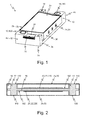
- FIG. 1 shows a three-dimensional view of an inventive power semiconductor module 1, in which the cuboid basic shape is clearly visible.
- the power semiconductor module 1 thus has two main sides 2 a / b, on each of which closely adjacent to the longitudinal 3 a / b and narrow sides 4 a / b in opposite corners, the connection means 110, 120, 130, 140 are arranged for the cooling liquid. These connection devices 110, 120, 130, 140 are part of the cooling device 10 of the power semiconductor module 1.
- a flow outlet 120 and a return flow 140 are shown here.
- the cooling device 10 between the main surfaces 2 a / b penetrating recesses 18 are provided, which serve in the juxtaposition of a plurality of power semiconductor modules 1 to the connection.
- the housing 30 of the power semiconductor module 1 which covers the recess of the U-shaped cooling device 10 and thereby forms essential parts of the first main side 2a. Covered by the housing 30 and not visible, the power electronic circuit 22 of the power electronic switching device 20 of the power semiconductor module 1 is arranged. Load connection devices 24, 26, here load output connection devices 26, are visible from the power electronic switching device 20. and control terminal devices 28. These penetrate the housing 30 at associated recesses 34, 36, 38, the load connection devices 24, 26 at longitudinal 3a / b, the control connection devices 28 at a narrow side 4a of the power semiconductor module 1.
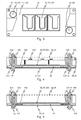
- FIG. 2 schematically shows a plan view from the direction of a longitudinal side 3a on a section through a power semiconductor module according to the invention 1. Shown here is a double-U-shaped cooling device 10 with a flow outlet 120 and a return drain 140 on a first main page 2a, while the respectively corresponding flow inlet 110 and the return inflow 130 are arranged on the second main side 2b. Between Vor- 12 and return 14, the flow-through cooling volume 16 is arranged.
- This cooling volume 16 here has only one chamber, which are assigned to two cooling surfaces 160, 162. On each of the two cooling surfaces 160, 162 switching modules 220 of the power electronic circuit 22 are arranged. In each case two opposite arranged switching modules 220 are associated with a phase of a three-phase inverter circuit.
- the housing 30 of this power semiconductor module 1 is formed as a dust-proof and moisture-proof encapsulation, which has only openings, not shown recesses 34, 36, 38, for carrying out the necessary external connection devices, and moreover both the power electronic circuit 22, as well the entire cooling device 10 surrounds.
- the necessary connection devices here are the four connection devices 110, 120, 130, 140 for the cooling liquid, and the load 24, 26 and control connection line 28 of the power electronic switching device 20, not shown.
- FIG. 3 shows a plan view from the direction of a main page 2a on an inventive power semiconductor module 1 without housing. Shown here is again a U-shaped cooling device 10 with a flow outlet 120 and a return drain 140 in opposite corners of the first main side 2a. In addition, in all corners of the cooling device 10 from the first 2a to second main side 2b hin manualde not connected to the cooling circuit recesses 18 are provided, which serve to connect to other power semiconductor modules, thereby screw connections for clamping the power semiconductor modules can be arranged to each other.
- a cooling surface 160 on the three switching modules 220 of the power electronic circuit 22 are arranged.
- the load connection devices 24, 26 extending from these submodules 220 to the longitudinal sides 3 a / b are, like the auxiliary connection device 28 extending from these submodules 220 to a narrow side 4 a / b, not shown.
- FIGS. 4 and 5 schematically show plan views from the direction of a longitudinal side 3a on a section through a further inventive power semiconductor module 1.
- a U-shaped cooling device 10 which completely forms a second main side 2b and the two narrow sides 4 a / b of the power semiconductor module 1.
- the cooling device 10 forms a part of the first main side 2a, as well as parts of the two longitudinal sides 3 a / b (see. Fig. 1 ).
- the remaining parts of the first main side 2 a, as well as the remaining parts of the two longitudinal sides 3 a / b are formed by the housing 30.
- three switching modules 220 of the power electronic circuit 22 are arranged on a cooling surface 160 of the cooling device 10 and are in thermal contact with the cooling liquid by means of this.
- the cooling liquid of the flow 12 arrives at the power semiconductor module 1 according to Fig. 4 by a feed flow 110 at the second main side 2b in the cooling device 10 and is divided there by means of a first branch 122 into two partial streams.
- the essential part of the cooling liquid leaves the cooling device 10 of the power semiconductor module 1 through the flow outlet 120 at the first main side 2a, while a small portion of the cooling liquid flows through the cooling volume 16 with adjacent cooling surface 160.
- the cooling fluid of the return 14 passes through this into the cooling device 10 and combines at a second branch 142 with the cooling liquid, which has flowed through the cooling volume 16.
- the return 14 then exits the cooler 10 through the return drain 140 on the first main side 2a.
- this power semiconductor module 1 also has an internal control board 240, which is connected in a customary manner to the switching modules 220 and provides driver functionality for the power electronic circuit 22.
- This internal control board 240 has as part of the power electronic switching device 20 on a narrow side 4a of the power semiconductor module 1, a control terminal device 28, which projects through a recess 38 of the housing 30.
- FIG. 5 shows basically the identical power semiconductor module 1, in which case the internal control board is not shown here, with identical connection devices. However, here the function of the connection means for cooling liquid is changed since the return inflow 130 is arranged on the first 2a and the return outflow 140 on the second main side 2b. However, this is only a functional, not a constructive change.
- the power semiconductor module is according to 4 and 5 thus suitable for different flow directions of the pre 12 and return 14. With increased demands on the efficiency of the first, second or both branches this suitability for any flow direction can also be abandoned.
- FIG. 6 shows a three-dimensional view of a first embodiment of the inventive arrangement 100. Shown is a plurality of arrangable power semiconductor modules 1, each with two connection means for cooling liquid on opposite main sides 2 a / b, with Lastan gleich wornen 24, 26 on the respective longitudinal sides 3 a / b and with Steueran gleich wornen 28 on the respective narrow sides 4a.
- the connection devices By means of the connection devices, the supply 12 and return 14 of the power semiconductor modules 1 is connected to a cooling circuit.
- the feed flow and the return flow of a power semiconductor module with the return flow of the subsequent power semiconductor module are connected directly exclusively with additional arrangement of external sealing means between the associated connection means to be connected.
- the power semiconductor modules 1 are screwed together, cf. Fig. 3 , or non-positively connected by means of a clamping device.
- the load input terminal devices 24, here the DC connection devices, are a first longitudinal side 3a and the load output terminal devices 26, here the AC voltage connection devices, are at the opposite longitudinal sides 3b arranged and penetrate the respective housing at associated recesses 34, 36.
- This embodiment provides enormous benefits for a trainee inverter circuit, since thus the DC voltage is separated from the AC voltage side.
- the connection to a DC voltage intermediate circuit can be provided in a compact and low-inductance manner on the DC voltage side.
- the AC-side connection can be provided according to requirements due to sufficient space.
- the auxiliary terminal devices 28 are provided on a narrow side 4a and therefore do not affect the design freedom for the load connections in any way.
- the auxiliary terminal devices 28 are connected to a multipart external control board 40, which may optionally have a suitable own housing as shown for dust and moisture-proof encapsulation.
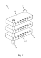
- FIG. 7 shows a three-dimensional view of a second embodiment of the inventive arrangement 100. Shown is a plurality of stackable power semiconductor modules 1, each with two connection means for cooling liquid on opposite main sides and with Lastan gleich Steinen 24, 26 on the respective longitudinal sides 3 a / b. The control terminal devices on the respective narrow sides are not shown.
- the connection devices By means of the connection devices, the supply 12 and return 14 of the power semiconductor modules 1 is connected to a cooling circuit.
- the feed flow and the return flow of a power semiconductor module with the return flow of the subsequent power semiconductor module are indirectly connected with additional arrangement of sealing means and flow-through spacers between the associated connection means to be connected.
- the assembly 100 preferably only the respective liquid-tight connections are made. This results in a composite that can be arranged in a holding device, not shown.
- the power semiconductor modules possibly with the addition of necessary spacers, be screwed together, cf. Fig. 3 ,
Landscapes
- Engineering & Computer Science (AREA)
- Microelectronics & Electronic Packaging (AREA)
- Physics & Mathematics (AREA)
- Thermal Sciences (AREA)
- Cooling Or The Like Of Semiconductors Or Solid State Devices (AREA)
- Inverter Devices (AREA)
- Cooling Or The Like Of Electrical Apparatus (AREA)
Applications Claiming Priority (1)
| Application Number | Priority Date | Filing Date | Title |
|---|---|---|---|
| DE102012206264A DE102012206264A1 (de) | 2012-04-17 | 2012-04-17 | Anreihbares flüssigkeitsgekühltes Leistungshalbleitermodul und Anordnung hiermit |
Publications (3)
| Publication Number | Publication Date |
|---|---|
| EP2654392A2 true EP2654392A2 (fr) | 2013-10-23 |
| EP2654392A3 EP2654392A3 (fr) | 2017-02-15 |
| EP2654392B1 EP2654392B1 (fr) | 2018-04-04 |
Family
ID=47664195
Family Applications (1)
| Application Number | Title | Priority Date | Filing Date |
|---|---|---|---|
| EP13154311.8A Active EP2654392B1 (fr) | 2012-04-17 | 2013-02-07 | Module semi-conducteur de puissance refroidi par liquide pouvant être joint et agencement à cet effet |
Country Status (6)
| Country | Link |
|---|---|
| US (1) | US9320182B2 (fr) |
| EP (1) | EP2654392B1 (fr) |
| JP (1) | JP6205164B2 (fr) |
| KR (1) | KR20130117670A (fr) |
| CN (2) | CN103379806B (fr) |
| DE (1) | DE102012206264A1 (fr) |
Cited By (1)
| Publication number | Priority date | Publication date | Assignee | Title |
|---|---|---|---|---|
| EP3206468A1 (fr) * | 2016-02-15 | 2017-08-16 | Siemens Aktiengesellschaft | Convertisseur dote d'un circuit intermediaire a tension continue |
Families Citing this family (15)
| Publication number | Priority date | Publication date | Assignee | Title |
|---|---|---|---|---|
| DE102012206264A1 (de) * | 2012-04-17 | 2013-10-17 | Semikron Elektronik Gmbh & Co. Kg | Anreihbares flüssigkeitsgekühltes Leistungshalbleitermodul und Anordnung hiermit |
| DE102013112110A1 (de) * | 2013-11-04 | 2015-05-07 | Phoenix Contact Gmbh & Co. Kg | Funktionskomponentenoberteil für ein Komponentenaufbausystem |
| CN104617064B (zh) * | 2013-11-04 | 2017-05-10 | 江苏宏微科技股份有限公司 | 叠加型功率模块 |
| US20180235110A1 (en) * | 2017-02-16 | 2018-08-16 | Lam Research Corporation | Cooling system for rf power electronics |
| DE102017104123B3 (de) * | 2017-02-28 | 2018-04-26 | Harting Electric Gmbh & Co. Kg | Schutztrennvorrichtung für eine Rechtecksteckverbindung |
| US10178800B2 (en) * | 2017-03-30 | 2019-01-08 | Honeywell International Inc. | Support structure for electronics having fluid passageway for convective heat transfer |
| CN107370385A (zh) * | 2017-08-01 | 2017-11-21 | 合肥华耀电子工业有限公司 | 一种新型液冷dc/dc电源 |
| JP6743782B2 (ja) * | 2017-08-11 | 2020-08-19 | 株式会社デンソー | 電力変換装置 |
| US10757809B1 (en) | 2017-11-13 | 2020-08-25 | Telephonics Corporation | Air-cooled heat exchanger and thermal arrangement for stacked electronics |
| DE102018131855A1 (de) | 2018-12-12 | 2020-06-18 | Semikron Elektronik Gmbh & Co. Kg | Leistungshalbleitermodul mit einem Druckkörper und mit einem Druckeinleitkörper, Leistungshalbleiteranordnung hiermit sowie Leistungshalbleitersystem hiermit |
| CN111365893B (zh) * | 2019-12-10 | 2021-12-10 | 中国船舶重工集团公司第七一六研究所 | 一种液冷服务器的半导体除湿装置控制方法 |
| DE102020208053A1 (de) * | 2020-04-03 | 2021-10-07 | Volkswagen Aktiengesellschaft | Fahrzeug, zentrale recheneinheit, module, herstellungsverfahren und fahrzeug, kühllamelle, taschenmodul, hauptrahmen |
| US12363874B2 (en) | 2020-04-03 | 2025-07-15 | Volkswagen Aktiengesellschaft | Vehicle and main frame for mounting and connecting vehicular components |
| CN115299186A (zh) | 2020-04-03 | 2022-11-04 | 大众汽车股份公司 | 载具、主框架、模块凹处、电子模块和印刷电路板 |
| US11502349B2 (en) | 2020-08-31 | 2022-11-15 | Borgwarner, Inc. | Cooling manifold assembly |
Citations (2)
| Publication number | Priority date | Publication date | Assignee | Title |
|---|---|---|---|---|
| DE10316356A1 (de) | 2003-04-10 | 2004-11-11 | Semikron Elektronik Gmbh | Modular aufgebautes Leistungshalbleitermodul |
| EP1815514B1 (fr) | 2004-11-24 | 2008-04-23 | Danfoss Silicon Power GmbH | Module de distribution de flux et pile de modules de distribution de flux |
Family Cites Families (16)
| Publication number | Priority date | Publication date | Assignee | Title |
|---|---|---|---|---|
| US4841355A (en) * | 1988-02-10 | 1989-06-20 | Amdahl Corporation | Three-dimensional microelectronic package for semiconductor chips |
| EP0669653A1 (fr) * | 1994-02-21 | 1995-08-30 | ABB Management AG | Module semi-conducteur de puissance et circuit avec au moins deux modules semi-conducteurs |
| CN2439735Y (zh) * | 2000-09-18 | 2001-07-18 | 中国科学院安徽光学精密机械研究所 | 大功率固体激光器循环水冷热交换装置 |
| JP2005191082A (ja) * | 2003-12-24 | 2005-07-14 | Toyota Motor Corp | 電気機器の冷却装置 |
| JP4046703B2 (ja) * | 2004-03-04 | 2008-02-13 | 三菱電機株式会社 | ヒートシンク |
| JP2005332863A (ja) * | 2004-05-18 | 2005-12-02 | Denso Corp | パワースタック |
| US8149579B2 (en) * | 2008-03-28 | 2012-04-03 | Johnson Controls Technology Company | Cooling member |
| JP2008198751A (ja) * | 2007-02-12 | 2008-08-28 | Denso Corp | 冷却器及びこれを用いた電力変換装置 |
| US7608924B2 (en) * | 2007-05-03 | 2009-10-27 | Delphi Technologies, Inc. | Liquid cooled power electronic circuit comprising stacked direct die cooled packages |
| JP5241344B2 (ja) * | 2008-06-30 | 2013-07-17 | 日立オートモティブシステムズ株式会社 | パワーモジュール及び電力変換装置 |
| JP5343616B2 (ja) * | 2009-02-25 | 2013-11-13 | 株式会社デンソー | 電力変換装置 |
| US7952875B2 (en) * | 2009-05-29 | 2011-05-31 | GM Global Technology Operations LLC | Stacked busbar assembly with integrated cooling |
| US20130032230A1 (en) * | 2010-04-13 | 2013-02-07 | Danfoss Silicon Power Gmbh | Flow distributor |
| JP5115632B2 (ja) * | 2010-06-30 | 2013-01-09 | 株式会社デンソー | 半導体装置 |
| DE102012206264A1 (de) * | 2012-04-17 | 2013-10-17 | Semikron Elektronik Gmbh & Co. Kg | Anreihbares flüssigkeitsgekühltes Leistungshalbleitermodul und Anordnung hiermit |
| DE102013103116B3 (de) * | 2013-03-27 | 2014-09-18 | Semikron Elektronik Gmbh & Co. Kg | Leistungshalbleitermodul und Verfahren zur Herstellung eines Leistungshalbleitermoduls |
-
2012
- 2012-04-17 DE DE102012206264A patent/DE102012206264A1/de not_active Withdrawn
-
2013
- 2013-02-07 EP EP13154311.8A patent/EP2654392B1/fr active Active
- 2013-04-05 KR KR1020130037367A patent/KR20130117670A/ko not_active Abandoned
- 2013-04-16 JP JP2013085612A patent/JP6205164B2/ja not_active Expired - Fee Related
- 2013-04-17 US US13/865,177 patent/US9320182B2/en not_active Expired - Fee Related
- 2013-04-17 CN CN201310133968.7A patent/CN103379806B/zh active Active
- 2013-04-17 CN CN201320194852XU patent/CN203219678U/zh not_active Expired - Lifetime
Patent Citations (2)
| Publication number | Priority date | Publication date | Assignee | Title |
|---|---|---|---|---|
| DE10316356A1 (de) | 2003-04-10 | 2004-11-11 | Semikron Elektronik Gmbh | Modular aufgebautes Leistungshalbleitermodul |
| EP1815514B1 (fr) | 2004-11-24 | 2008-04-23 | Danfoss Silicon Power GmbH | Module de distribution de flux et pile de modules de distribution de flux |
Cited By (3)
| Publication number | Priority date | Publication date | Assignee | Title |
|---|---|---|---|---|
| EP3206468A1 (fr) * | 2016-02-15 | 2017-08-16 | Siemens Aktiengesellschaft | Convertisseur dote d'un circuit intermediaire a tension continue |
| RU2659092C1 (ru) * | 2016-02-15 | 2018-06-28 | Сименс Акциенгезелльшафт | Преобразователь, имеющий промежуточный контур постоянного напряжения |
| US10141860B2 (en) | 2016-02-15 | 2018-11-27 | Siemens Aktiengesellschaft | Converter with DC link |
Also Published As
| Publication number | Publication date |
|---|---|
| US9320182B2 (en) | 2016-04-19 |
| CN103379806B (zh) | 2018-01-16 |
| JP6205164B2 (ja) | 2017-09-27 |
| EP2654392B1 (fr) | 2018-04-04 |
| US20130271916A1 (en) | 2013-10-17 |
| CN103379806A (zh) | 2013-10-30 |
| EP2654392A3 (fr) | 2017-02-15 |
| JP2013222973A (ja) | 2013-10-28 |
| KR20130117670A (ko) | 2013-10-28 |
| DE102012206264A1 (de) | 2013-10-17 |
| CN203219678U (zh) | 2013-09-25 |
Similar Documents
| Publication | Publication Date | Title |
|---|---|---|
| EP2654392B1 (fr) | Module semi-conducteur de puissance refroidi par liquide pouvant être joint et agencement à cet effet | |
| EP2654391B1 (fr) | Agencement refroidi par liquide avec modules semi-conducteurs de puissance pouvant être joints et au moins un dispositif de condensateur et module semi-conducteur de puissance à cet effet | |
| EP2364581B1 (fr) | Module redresseur de courant à système de barres refroidi | |
| EP2356894B1 (fr) | Module redresseur de courant avec rails refroidis | |
| EP2364580B1 (fr) | Module redresseur de courant à système de barres refroidi | |
| EP1848260B1 (fr) | Onduleur | |
| DE112013005692T5 (de) | Invertervorrichtung | |
| DE102012210677A1 (de) | Leistungsmodul-Kühlsystem | |
| DE102013222496A1 (de) | Elektrischer Leistungswandler | |
| DE102016207701A1 (de) | Leistungsumsetzer und Schienenfahrzeug | |
| WO2012152551A1 (fr) | Système électronique de puissance muni d'un dispositif de refroidissement par liquide | |
| DE102012215787A1 (de) | Leistungselektronisches System mit Flüssigkeitskühleinrichtung | |
| DE102017117708A1 (de) | Halbleitereinrichtung mit einem Schaltelement, das eine Potentialschwankung unterdrückt | |
| EP2528091A2 (fr) | Système électronique de puissance avec sous-systèmes et dispositif de refroidissement | |
| DE102017005315A1 (de) | Batteriekasten | |
| DE102012222011A1 (de) | Leistungshalbleitermodulsystem | |
| EP4410063A1 (fr) | Module de puissance, en particulier pour l'électronique de puissance d'un véhicule | |
| EP2521432A2 (fr) | Agencement de puissance électronique doté d'un refroidissement de liquide | |
| DE112014005253T5 (de) | Gussgehäuse für einen konfigurierbaren Leistungswandler | |
| DE202009012751U1 (de) | Stromrichteranordnung | |
| DE112021007331T5 (de) | Vorrichtung zum Umsetzen elektrischer Leistung | |
| DE102019133952A1 (de) | Leistungselektronisches System mit einem Gehäuse, einer Kühleinrichtung, einem Leistungshalbleitermodul und einer Kondensatoreinrichtung | |
| DE102017106515B4 (de) | 3-Pegel-Leistungsmodul | |
| EP1739804A1 (fr) | Rail de support conducteur de courant d'un ou de plusieurs appareils électriques | |
| EP2803252A2 (fr) | Système de module d'électronique de puissance avec système de refroidissement incorporé |
Legal Events
| Date | Code | Title | Description |
|---|---|---|---|
| PUAI | Public reference made under article 153(3) epc to a published international application that has entered the european phase |
Free format text: ORIGINAL CODE: 0009012 |
|
| AK | Designated contracting states |
Kind code of ref document: A2 Designated state(s): AL AT BE BG CH CY CZ DE DK EE ES FI FR GB GR HR HU IE IS IT LI LT LU LV MC MK MT NL NO PL PT RO RS SE SI SK SM TR |
|
| AX | Request for extension of the european patent |
Extension state: BA ME |
|
| 17P | Request for examination filed |
Effective date: 20160711 |
|
| PUAL | Search report despatched |
Free format text: ORIGINAL CODE: 0009013 |
|
| AK | Designated contracting states |
Kind code of ref document: A3 Designated state(s): AL AT BE BG CH CY CZ DE DK EE ES FI FR GB GR HR HU IE IS IT LI LT LU LV MC MK MT NL NO PL PT RO RS SE SI SK SM TR |
|
| AX | Request for extension of the european patent |
Extension state: BA ME |
|
| RIC1 | Information provided on ipc code assigned before grant |
Ipc: H05K 7/20 20060101AFI20170112BHEP Ipc: H01L 23/473 20060101ALI20170112BHEP Ipc: H01L 25/07 20060101ALI20170112BHEP Ipc: H01L 25/11 20060101ALI20170112BHEP |
|
| RBV | Designated contracting states (corrected) |
Designated state(s): AL AT BE BG CH CY CZ DE DK EE ES FI FR GB GR HR HU IE IS IT LI LT LU LV MC MK MT NL NO PL PT RO RS SE SI SK SM TR |
|
| GRAP | Despatch of communication of intention to grant a patent |
Free format text: ORIGINAL CODE: EPIDOSNIGR1 |
|
| STAA | Information on the status of an ep patent application or granted ep patent |
Free format text: STATUS: GRANT OF PATENT IS INTENDED |
|
| INTG | Intention to grant announced |
Effective date: 20180105 |
|
| GRAS | Grant fee paid |
Free format text: ORIGINAL CODE: EPIDOSNIGR3 |
|
| GRAA | (expected) grant |
Free format text: ORIGINAL CODE: 0009210 |
|
| STAA | Information on the status of an ep patent application or granted ep patent |
Free format text: STATUS: THE PATENT HAS BEEN GRANTED |
|
| AK | Designated contracting states |
Kind code of ref document: B1 Designated state(s): AL AT BE BG CH CY CZ DE DK EE ES FI FR GB GR HR HU IE IS IT LI LT LU LV MC MK MT NL NO PL PT RO RS SE SI SK SM TR |
|
| REG | Reference to a national code |
Ref country code: GB Ref legal event code: FG4D Free format text: NOT ENGLISH |
|
| REG | Reference to a national code |
Ref country code: CH Ref legal event code: EP |
|
| REG | Reference to a national code |
Ref country code: AT Ref legal event code: REF Ref document number: 986954 Country of ref document: AT Kind code of ref document: T Effective date: 20180415 |
|
| REG | Reference to a national code |
Ref country code: IE Ref legal event code: FG4D Free format text: LANGUAGE OF EP DOCUMENT: GERMAN |
|
| REG | Reference to a national code |
Ref country code: DE Ref legal event code: R096 Ref document number: 502013009814 Country of ref document: DE |
|
| REG | Reference to a national code |
Ref country code: NL Ref legal event code: MP Effective date: 20180404 |
|
| REG | Reference to a national code |
Ref country code: LT Ref legal event code: MG4D |
|
| PG25 | Lapsed in a contracting state [announced via postgrant information from national office to epo] |
Ref country code: NL Free format text: LAPSE BECAUSE OF FAILURE TO SUBMIT A TRANSLATION OF THE DESCRIPTION OR TO PAY THE FEE WITHIN THE PRESCRIBED TIME-LIMIT Effective date: 20180404 |
|
| PG25 | Lapsed in a contracting state [announced via postgrant information from national office to epo] |
Ref country code: ES Free format text: LAPSE BECAUSE OF FAILURE TO SUBMIT A TRANSLATION OF THE DESCRIPTION OR TO PAY THE FEE WITHIN THE PRESCRIBED TIME-LIMIT Effective date: 20180404 Ref country code: AL Free format text: LAPSE BECAUSE OF FAILURE TO SUBMIT A TRANSLATION OF THE DESCRIPTION OR TO PAY THE FEE WITHIN THE PRESCRIBED TIME-LIMIT Effective date: 20180404 Ref country code: PL Free format text: LAPSE BECAUSE OF FAILURE TO SUBMIT A TRANSLATION OF THE DESCRIPTION OR TO PAY THE FEE WITHIN THE PRESCRIBED TIME-LIMIT Effective date: 20180404 Ref country code: SE Free format text: LAPSE BECAUSE OF FAILURE TO SUBMIT A TRANSLATION OF THE DESCRIPTION OR TO PAY THE FEE WITHIN THE PRESCRIBED TIME-LIMIT Effective date: 20180404 Ref country code: NO Free format text: LAPSE BECAUSE OF FAILURE TO SUBMIT A TRANSLATION OF THE DESCRIPTION OR TO PAY THE FEE WITHIN THE PRESCRIBED TIME-LIMIT Effective date: 20180704 Ref country code: FI Free format text: LAPSE BECAUSE OF FAILURE TO SUBMIT A TRANSLATION OF THE DESCRIPTION OR TO PAY THE FEE WITHIN THE PRESCRIBED TIME-LIMIT Effective date: 20180404 Ref country code: BG Free format text: LAPSE BECAUSE OF FAILURE TO SUBMIT A TRANSLATION OF THE DESCRIPTION OR TO PAY THE FEE WITHIN THE PRESCRIBED TIME-LIMIT Effective date: 20180704 Ref country code: LT Free format text: LAPSE BECAUSE OF FAILURE TO SUBMIT A TRANSLATION OF THE DESCRIPTION OR TO PAY THE FEE WITHIN THE PRESCRIBED TIME-LIMIT Effective date: 20180404 |
|
| PG25 | Lapsed in a contracting state [announced via postgrant information from national office to epo] |
Ref country code: GR Free format text: LAPSE BECAUSE OF FAILURE TO SUBMIT A TRANSLATION OF THE DESCRIPTION OR TO PAY THE FEE WITHIN THE PRESCRIBED TIME-LIMIT Effective date: 20180705 Ref country code: RS Free format text: LAPSE BECAUSE OF FAILURE TO SUBMIT A TRANSLATION OF THE DESCRIPTION OR TO PAY THE FEE WITHIN THE PRESCRIBED TIME-LIMIT Effective date: 20180404 Ref country code: HR Free format text: LAPSE BECAUSE OF FAILURE TO SUBMIT A TRANSLATION OF THE DESCRIPTION OR TO PAY THE FEE WITHIN THE PRESCRIBED TIME-LIMIT Effective date: 20180404 Ref country code: LV Free format text: LAPSE BECAUSE OF FAILURE TO SUBMIT A TRANSLATION OF THE DESCRIPTION OR TO PAY THE FEE WITHIN THE PRESCRIBED TIME-LIMIT Effective date: 20180404 |
|
| PG25 | Lapsed in a contracting state [announced via postgrant information from national office to epo] |
Ref country code: PT Free format text: LAPSE BECAUSE OF FAILURE TO SUBMIT A TRANSLATION OF THE DESCRIPTION OR TO PAY THE FEE WITHIN THE PRESCRIBED TIME-LIMIT Effective date: 20180806 |
|
| REG | Reference to a national code |
Ref country code: DE Ref legal event code: R097 Ref document number: 502013009814 Country of ref document: DE |
|
| PG25 | Lapsed in a contracting state [announced via postgrant information from national office to epo] |
Ref country code: CZ Free format text: LAPSE BECAUSE OF FAILURE TO SUBMIT A TRANSLATION OF THE DESCRIPTION OR TO PAY THE FEE WITHIN THE PRESCRIBED TIME-LIMIT Effective date: 20180404 Ref country code: RO Free format text: LAPSE BECAUSE OF FAILURE TO SUBMIT A TRANSLATION OF THE DESCRIPTION OR TO PAY THE FEE WITHIN THE PRESCRIBED TIME-LIMIT Effective date: 20180404 Ref country code: DK Free format text: LAPSE BECAUSE OF FAILURE TO SUBMIT A TRANSLATION OF THE DESCRIPTION OR TO PAY THE FEE WITHIN THE PRESCRIBED TIME-LIMIT Effective date: 20180404 Ref country code: EE Free format text: LAPSE BECAUSE OF FAILURE TO SUBMIT A TRANSLATION OF THE DESCRIPTION OR TO PAY THE FEE WITHIN THE PRESCRIBED TIME-LIMIT Effective date: 20180404 Ref country code: SK Free format text: LAPSE BECAUSE OF FAILURE TO SUBMIT A TRANSLATION OF THE DESCRIPTION OR TO PAY THE FEE WITHIN THE PRESCRIBED TIME-LIMIT Effective date: 20180404 |
|
| PLBE | No opposition filed within time limit |
Free format text: ORIGINAL CODE: 0009261 |
|
| STAA | Information on the status of an ep patent application or granted ep patent |
Free format text: STATUS: NO OPPOSITION FILED WITHIN TIME LIMIT |
|
| PG25 | Lapsed in a contracting state [announced via postgrant information from national office to epo] |
Ref country code: IT Free format text: LAPSE BECAUSE OF FAILURE TO SUBMIT A TRANSLATION OF THE DESCRIPTION OR TO PAY THE FEE WITHIN THE PRESCRIBED TIME-LIMIT Effective date: 20180404 Ref country code: SM Free format text: LAPSE BECAUSE OF FAILURE TO SUBMIT A TRANSLATION OF THE DESCRIPTION OR TO PAY THE FEE WITHIN THE PRESCRIBED TIME-LIMIT Effective date: 20180404 |
|
| 26N | No opposition filed |
Effective date: 20190107 |
|
| PG25 | Lapsed in a contracting state [announced via postgrant information from national office to epo] |
Ref country code: SI Free format text: LAPSE BECAUSE OF FAILURE TO SUBMIT A TRANSLATION OF THE DESCRIPTION OR TO PAY THE FEE WITHIN THE PRESCRIBED TIME-LIMIT Effective date: 20180404 |
|
| REG | Reference to a national code |
Ref country code: CH Ref legal event code: PL |
|
| PG25 | Lapsed in a contracting state [announced via postgrant information from national office to epo] |
Ref country code: MC Free format text: LAPSE BECAUSE OF FAILURE TO SUBMIT A TRANSLATION OF THE DESCRIPTION OR TO PAY THE FEE WITHIN THE PRESCRIBED TIME-LIMIT Effective date: 20180404 Ref country code: LU Free format text: LAPSE BECAUSE OF NON-PAYMENT OF DUE FEES Effective date: 20190207 |
|
| REG | Reference to a national code |
Ref country code: BE Ref legal event code: MM Effective date: 20190228 |
|
| REG | Reference to a national code |
Ref country code: IE Ref legal event code: MM4A |
|
| PG25 | Lapsed in a contracting state [announced via postgrant information from national office to epo] |
Ref country code: LI Free format text: LAPSE BECAUSE OF NON-PAYMENT OF DUE FEES Effective date: 20190228 Ref country code: CH Free format text: LAPSE BECAUSE OF NON-PAYMENT OF DUE FEES Effective date: 20190228 |
|
| PG25 | Lapsed in a contracting state [announced via postgrant information from national office to epo] |
Ref country code: IE Free format text: LAPSE BECAUSE OF NON-PAYMENT OF DUE FEES Effective date: 20190207 |
|
| PG25 | Lapsed in a contracting state [announced via postgrant information from national office to epo] |
Ref country code: BE Free format text: LAPSE BECAUSE OF NON-PAYMENT OF DUE FEES Effective date: 20190228 |
|
| PG25 | Lapsed in a contracting state [announced via postgrant information from national office to epo] |
Ref country code: TR Free format text: LAPSE BECAUSE OF FAILURE TO SUBMIT A TRANSLATION OF THE DESCRIPTION OR TO PAY THE FEE WITHIN THE PRESCRIBED TIME-LIMIT Effective date: 20180404 |
|
| REG | Reference to a national code |
Ref country code: AT Ref legal event code: MM01 Ref document number: 986954 Country of ref document: AT Kind code of ref document: T Effective date: 20190207 |
|
| PG25 | Lapsed in a contracting state [announced via postgrant information from national office to epo] |
Ref country code: AT Free format text: LAPSE BECAUSE OF NON-PAYMENT OF DUE FEES Effective date: 20190207 |
|
| PG25 | Lapsed in a contracting state [announced via postgrant information from national office to epo] |
Ref country code: MT Free format text: LAPSE BECAUSE OF FAILURE TO SUBMIT A TRANSLATION OF THE DESCRIPTION OR TO PAY THE FEE WITHIN THE PRESCRIBED TIME-LIMIT Effective date: 20180404 |
|
| PG25 | Lapsed in a contracting state [announced via postgrant information from national office to epo] |
Ref country code: CY Free format text: LAPSE BECAUSE OF FAILURE TO SUBMIT A TRANSLATION OF THE DESCRIPTION OR TO PAY THE FEE WITHIN THE PRESCRIBED TIME-LIMIT Effective date: 20180404 |
|
| PG25 | Lapsed in a contracting state [announced via postgrant information from national office to epo] |
Ref country code: IS Free format text: LAPSE BECAUSE OF FAILURE TO SUBMIT A TRANSLATION OF THE DESCRIPTION OR TO PAY THE FEE WITHIN THE PRESCRIBED TIME-LIMIT Effective date: 20180804 |
|
| PG25 | Lapsed in a contracting state [announced via postgrant information from national office to epo] |
Ref country code: HU Free format text: LAPSE BECAUSE OF FAILURE TO SUBMIT A TRANSLATION OF THE DESCRIPTION OR TO PAY THE FEE WITHIN THE PRESCRIBED TIME-LIMIT; INVALID AB INITIO Effective date: 20130207 |
|
| PG25 | Lapsed in a contracting state [announced via postgrant information from national office to epo] |
Ref country code: MK Free format text: LAPSE BECAUSE OF FAILURE TO SUBMIT A TRANSLATION OF THE DESCRIPTION OR TO PAY THE FEE WITHIN THE PRESCRIBED TIME-LIMIT Effective date: 20180404 |
|
| PGFP | Annual fee paid to national office [announced via postgrant information from national office to epo] |
Ref country code: FR Payment date: 20241231 Year of fee payment: 13 |
|
| PGFP | Annual fee paid to national office [announced via postgrant information from national office to epo] |
Ref country code: GB Payment date: 20250102 Year of fee payment: 13 |
|
| REG | Reference to a national code |
Ref country code: DE Ref legal event code: R081 Ref document number: 502013009814 Country of ref document: DE Owner name: SEMIKRON DANFOSS ELEKTRONIK GMBH & CO. KG, DE Free format text: FORMER OWNER: SEMIKRON ELEKTRONIK GMBH & CO. KG, 90431 NUERNBERG, DE |
|
| PGFP | Annual fee paid to national office [announced via postgrant information from national office to epo] |
Ref country code: DE Payment date: 20260102 Year of fee payment: 14 |