EP2666745B1 - Gehäuse für eine elektronische Komponente und Verfahren zu dessen Herstellung - Google Patents
Gehäuse für eine elektronische Komponente und Verfahren zu dessen Herstellung Download PDFInfo
- Publication number
- EP2666745B1 EP2666745B1 EP13181356.0A EP13181356A EP2666745B1 EP 2666745 B1 EP2666745 B1 EP 2666745B1 EP 13181356 A EP13181356 A EP 13181356A EP 2666745 B1 EP2666745 B1 EP 2666745B1
- Authority
- EP
- European Patent Office
- Prior art keywords
- package
- electronic component
- silicon substrate
- electrodes
- insulating layer
- Prior art date
- Legal status (The legal status is an assumption and is not a legal conclusion. Google has not performed a legal analysis and makes no representation as to the accuracy of the status listed.)
- Active
Links
Images




Classifications
-
- H—ELECTRICITY
- H10—SEMICONDUCTOR DEVICES; ELECTRIC SOLID-STATE DEVICES NOT OTHERWISE PROVIDED FOR
- H10W—GENERIC PACKAGES, INTERCONNECTIONS, CONNECTORS OR OTHER CONSTRUCTIONAL DETAILS OF DEVICES COVERED BY CLASS H10
- H10W76/00—Containers; Fillings or auxiliary members therefor; Seals
- H10W76/10—Containers or parts thereof
- H10W76/12—Containers or parts thereof characterised by their shape
- H10W76/13—Containers comprising a conductive base serving as an interconnection
- H10W76/132—Containers comprising a conductive base serving as an interconnection having other interconnections through an insulated passage in the conductive base
-
- B—PERFORMING OPERATIONS; TRANSPORTING
- B81—MICROSTRUCTURAL TECHNOLOGY
- B81C—PROCESSES OR APPARATUS SPECIALLY ADAPTED FOR THE MANUFACTURE OR TREATMENT OF MICROSTRUCTURAL DEVICES OR SYSTEMS
- B81C1/00—Manufacture or treatment of devices or systems in or on a substrate
- B81C1/00015—Manufacture or treatment of devices or systems in or on a substrate for manufacturing microsystems
- B81C1/00261—Processes for packaging MEMS devices
- B81C1/00301—Connecting electric signal lines from the MEMS device with external electrical signal lines, e.g. through vias
-
- H—ELECTRICITY
- H10—SEMICONDUCTOR DEVICES; ELECTRIC SOLID-STATE DEVICES NOT OTHERWISE PROVIDED FOR
- H10H—INORGANIC LIGHT-EMITTING SEMICONDUCTOR DEVICES HAVING POTENTIAL BARRIERS
- H10H20/00—Individual inorganic light-emitting semiconductor devices having potential barriers, e.g. light-emitting diodes [LED]
- H10H20/80—Constructional details
- H10H20/85—Packages
- H10H20/8506—Containers
-
- B—PERFORMING OPERATIONS; TRANSPORTING
- B81—MICROSTRUCTURAL TECHNOLOGY
- B81B—MICROSTRUCTURAL DEVICES OR SYSTEMS, e.g. MICROMECHANICAL DEVICES
- B81B2207/00—Microstructural systems or auxiliary parts thereof
- B81B2207/09—Packages
- B81B2207/091—Arrangements for connecting external electrical signals to mechanical structures inside the package
- B81B2207/094—Feed-through, via
- B81B2207/096—Feed-through, via through the substrate
-
- B—PERFORMING OPERATIONS; TRANSPORTING
- B81—MICROSTRUCTURAL TECHNOLOGY
- B81C—PROCESSES OR APPARATUS SPECIALLY ADAPTED FOR THE MANUFACTURE OR TREATMENT OF MICROSTRUCTURAL DEVICES OR SYSTEMS
- B81C2203/00—Forming microstructural systems
- B81C2203/01—Packaging MEMS
- B81C2203/0118—Bonding a wafer on the substrate, i.e. where the cap consists of another wafer
-
- H—ELECTRICITY
- H10—SEMICONDUCTOR DEVICES; ELECTRIC SOLID-STATE DEVICES NOT OTHERWISE PROVIDED FOR
- H10H—INORGANIC LIGHT-EMITTING SEMICONDUCTOR DEVICES HAVING POTENTIAL BARRIERS
- H10H20/00—Individual inorganic light-emitting semiconductor devices having potential barriers, e.g. light-emitting diodes [LED]
- H10H20/80—Constructional details
- H10H20/85—Packages
- H10H20/857—Interconnections, e.g. lead-frames, bond wires or solder balls
-
- H—ELECTRICITY
- H10—SEMICONDUCTOR DEVICES; ELECTRIC SOLID-STATE DEVICES NOT OTHERWISE PROVIDED FOR
- H10H—INORGANIC LIGHT-EMITTING SEMICONDUCTOR DEVICES HAVING POTENTIAL BARRIERS
- H10H20/00—Individual inorganic light-emitting semiconductor devices having potential barriers, e.g. light-emitting diodes [LED]
- H10H20/80—Constructional details
- H10H20/85—Packages
- H10H20/858—Means for heat extraction or cooling
- H10H20/8585—Means for heat extraction or cooling being an interconnection
-
- H—ELECTRICITY
- H10—SEMICONDUCTOR DEVICES; ELECTRIC SOLID-STATE DEVICES NOT OTHERWISE PROVIDED FOR
- H10W—GENERIC PACKAGES, INTERCONNECTIONS, CONNECTORS OR OTHER CONSTRUCTIONAL DETAILS OF DEVICES COVERED BY CLASS H10
- H10W70/00—Package substrates; Interposers; Redistribution layers [RDL]
- H10W70/60—Insulating or insulated package substrates; Interposers; Redistribution layers
- H10W70/67—Insulating or insulated package substrates; Interposers; Redistribution layers characterised by their insulating layers or insulating parts
- H10W70/68—Shapes or dispositions thereof
- H10W70/682—Shapes or dispositions thereof comprising holes having chips therein
-
- H—ELECTRICITY
- H10—SEMICONDUCTOR DEVICES; ELECTRIC SOLID-STATE DEVICES NOT OTHERWISE PROVIDED FOR
- H10W—GENERIC PACKAGES, INTERCONNECTIONS, CONNECTORS OR OTHER CONSTRUCTIONAL DETAILS OF DEVICES COVERED BY CLASS H10
- H10W70/00—Package substrates; Interposers; Redistribution layers [RDL]
- H10W70/60—Insulating or insulated package substrates; Interposers; Redistribution layers
- H10W70/67—Insulating or insulated package substrates; Interposers; Redistribution layers characterised by their insulating layers or insulating parts
- H10W70/68—Shapes or dispositions thereof
- H10W70/685—Shapes or dispositions thereof comprising multiple insulating layers
-
- H—ELECTRICITY
- H10—SEMICONDUCTOR DEVICES; ELECTRIC SOLID-STATE DEVICES NOT OTHERWISE PROVIDED FOR
- H10W—GENERIC PACKAGES, INTERCONNECTIONS, CONNECTORS OR OTHER CONSTRUCTIONAL DETAILS OF DEVICES COVERED BY CLASS H10
- H10W72/00—Interconnections or connectors in packages
- H10W72/01—Manufacture or treatment
- H10W72/0198—Manufacture or treatment batch processes
-
- H—ELECTRICITY
- H10—SEMICONDUCTOR DEVICES; ELECTRIC SOLID-STATE DEVICES NOT OTHERWISE PROVIDED FOR
- H10W—GENERIC PACKAGES, INTERCONNECTIONS, CONNECTORS OR OTHER CONSTRUCTIONAL DETAILS OF DEVICES COVERED BY CLASS H10
- H10W72/00—Interconnections or connectors in packages
- H10W72/071—Connecting or disconnecting
- H10W72/072—Connecting or disconnecting of bump connectors
- H10W72/07231—Techniques
- H10W72/07236—Soldering or alloying
-
- H—ELECTRICITY
- H10—SEMICONDUCTOR DEVICES; ELECTRIC SOLID-STATE DEVICES NOT OTHERWISE PROVIDED FOR
- H10W—GENERIC PACKAGES, INTERCONNECTIONS, CONNECTORS OR OTHER CONSTRUCTIONAL DETAILS OF DEVICES COVERED BY CLASS H10
- H10W72/00—Interconnections or connectors in packages
- H10W72/071—Connecting or disconnecting
- H10W72/072—Connecting or disconnecting of bump connectors
- H10W72/07251—Connecting or disconnecting of bump connectors characterised by changes in properties of the bump connectors during connecting
-
- H—ELECTRICITY
- H10—SEMICONDUCTOR DEVICES; ELECTRIC SOLID-STATE DEVICES NOT OTHERWISE PROVIDED FOR
- H10W—GENERIC PACKAGES, INTERCONNECTIONS, CONNECTORS OR OTHER CONSTRUCTIONAL DETAILS OF DEVICES COVERED BY CLASS H10
- H10W72/00—Interconnections or connectors in packages
- H10W72/20—Bump connectors, e.g. solder bumps or copper pillars; Dummy bumps; Thermal bumps
-
- H—ELECTRICITY
- H10—SEMICONDUCTOR DEVICES; ELECTRIC SOLID-STATE DEVICES NOT OTHERWISE PROVIDED FOR
- H10W—GENERIC PACKAGES, INTERCONNECTIONS, CONNECTORS OR OTHER CONSTRUCTIONAL DETAILS OF DEVICES COVERED BY CLASS H10
- H10W74/00—Encapsulations, e.g. protective coatings
-
- H—ELECTRICITY
- H10—SEMICONDUCTOR DEVICES; ELECTRIC SOLID-STATE DEVICES NOT OTHERWISE PROVIDED FOR
- H10W—GENERIC PACKAGES, INTERCONNECTIONS, CONNECTORS OR OTHER CONSTRUCTIONAL DETAILS OF DEVICES COVERED BY CLASS H10
- H10W90/00—Package configurations
- H10W90/701—Package configurations characterised by the relative positions of pads or connectors relative to package parts
- H10W90/721—Package configurations characterised by the relative positions of pads or connectors relative to package parts of bump connectors
- H10W90/724—Package configurations characterised by the relative positions of pads or connectors relative to package parts of bump connectors between a chip and a stacked insulating package substrate, interposer or RDL
Definitions
- the present invention relates to an electronic component package and a method of manufacturing the same and an electronic component device and, more particularly, an electronic component package on which an electronic component such as an MEMS element, an optical semiconductor element, or the like is mounted and a method of manufacturing the same and an electronic component device.
- the electronic component package on which the electronic component such as the MEMS element, the optical semiconductor element, or the like is mounted.
- some packages have such a structure that a cavity in which the electronic component is mounted is provided in the center portion of a silicon substrate, and through electrodes are provided in a silicon substrate under the cavity.
- a first mask layer 200 in which opening portions 200x used to form through holes are provided is formed on a silicon wafer 100.
- the silicon wafer 100 is etched to pass through from its upper surface to its lower surface by using the first mask layer 200 as a mask, and thus through holes TH are formed.
- the first mask layer 200 is removed.
- a second mask layer 300 in which an opening portion 300x used to form a cavity is provided is formed on the silicon wafer 100.
- the silicon wafer 100 is etched up to the middle of a thickness by using the second mask layer 300 as a mask, and thus a cavity C is formed.
- the second mask layer 300 is removed.
- a plurality of package areas are defined on the silicon wafer 100, and the through holes TH and the cavity C are provided in each area.
- an insulating layer 400 made of a silicon oxide layer is formed on the whole surface of the silicon wafer 100 by thermally oxidizing the silicon wafer 100.
- through electrodes 500 are formed in the through holes TH in the silicon wafer 100 by the plating. At this time, the through electrodes 500 are formed in a state that they protrude from an upper surface and a lower surface of the silicon wafer 100 respectively.
- individual electronic component packages are obtained by cutting the silicon wafer 100.
- Patent Literature 1 Patent Application Publication (KOKAI) 2004-22990 )
- a metal is filled in through holes in a silicon substrate, then both surface sides of the silicon substrate are planarized by the polishing, and then the silicon substrate is processed by high-pressure annealing, thereby a density and adhesion of the plug metal are improved.
- Patent Literature 2 Patent Application Publication (KOKAI) Hei 6-169031
- an insulating layer made of a relatively soft polymer such as polyimide, and the like is formed on both surfaces of a silicon substrate, then wiring layers are formed thereon, and then an IC chip made of the same material as the silicon substrate is CCB-connected to the wiring layers, thereby a stress applied to connection portions is reduced.
- the through electrodes 500 filled in the through holes TH are formed to protrude from a bottom portion of the cavity C, and also their heights are varied on account of the essential characteristic of the plating. Therefore, a coplanarity of the through electrodes 500 on which the electronic component is mounted is not enough. As a result, in some cases a faulty connection is caused in mounting the high-performance electronic component, and such faulty connection becomes a factor of a reduction of yield.
- the method of improving the coplanarity by planarizing the through electrodes 500 may be considered.
- the through electrodes 500 are formed after the cavity C is formed, unevenness due to the cavity C exists on the silicon wafer 100. Therefore, it is difficult to planarize the through electrodes 500 in the cavity C by the CMP, or the like. For the same reason, it is extremely difficult to form fine wiring layers connected to the through electrodes 500 on a bottom surface of the cavity C.
- EP1749794A2 discloses a packaging structure in which electronic parts are mounted on a silicon circuit substrate having a structure in which wiring layers on both sides thereof are connected to each other through a through electrode, and a ring-shaped glass seal cap defining a cavity is anodically bonded to a portion of the silicon circuit substrate to hermetically seal the electronic parts.
- US2006/022036A1 discloses an LED package in which upper and lower surfaces of a silicon substrate are formed with an insulating layer. A cavity is defined by a reflecting structure provided on the insulating layer and an electrode on top of the insulating layer which connects to a through electrode formed beneath the reflecting structure.
- an electronic component package capable of obtaining a sufficient coplanarity of through electrodes even when a cavity is provided and also capable of responding easily to the case where various elements are built, in the electronic component package having such a structure that through electrodes are provided in a silicon substrate, and a method of manufacturing the same and an electronic component device.
- an electronic component package comprising: a package substrate portion constructed by a first silicon substrate in which at least two through holes are provided, a first insulating layer formed on upper and lower surface sides of the first silicon substrate and inner surface of the through holes, and first and second through electrodes filled respectively in the at least two through holes; and a frame portion formed from a second silicon substrate, the frame portion defining an opening extending from an upper surface to a lower surface of the frame portion and being stacked on top of a peripheral portion of the package substrate portion to constitute a cavity on the first silicon substrate, the first electrode being located in the cavity; wherein respective upper surfaces of the first and second through electrodes are coplanar with an upper surface of the first insulating layer formed on the upper surface side of the first silicon substrate, and respective lower surfaces of the first and second through electrodes are coplanar with a lower surface of the first insulating layer formed on the lower surface side of the first silicon substrate; and the first insulating layer formed on the upper surface of the first silicon substrate
- a method of manufacturing an electronic component package comprising the steps of: forming a package member by a method that includes a step of forming at least two through holes in a package region of a first silicon substrate, a step of forming a first insulating layer on upper and lower surfaces of the first silicon substrate and inner surface of the through holes, a step of filling first and second through electrodes respectively in the at least two through holes, and a step of planarizing the first and second through electrodes such that respective upper surfaces of the first and second through electrodes are coplanar with an upper surface of the first insulating layer formed on the upper surface side of the first silicon substrate and respective lower surfaces of the first and second through electrodes are coplanar with a lower surface of the first insulating layer formed on the lower surface side of the first silicon substrate, by polishing the first and second through electrodes; preparing a frame member formed from a second silicon substrate, and corresponding to a peripheral portion of the package region of the first silicon substrate, before or
- the through electrodes are formed in the silicon substrate, and then the package substrate portion is obtained by planarizing the through electrodes. Then, the cavity is constructed by providing the frame portion (silicon) on the peripheral portion of the package substrate portion.
- the through electrodes are formed in the flat silicon substrate in which the cavity is not provided, and then the frame portion is provided. Therefore, upper and lower surfaces of the through electrodes can be planarized unlike the prior art. As a result, the planarized through electrodes are arranged in the silicon substrate in the cavity. Also, when the plasma process is utilized, the frame portion can be joined to the package substrate portion by the low-temperature joining that does not damage the through electrodes.
- the electronic component package having such a structure that the cavity is provided on the package substrate portion by the frame portion and the through electrodes whose coplanarity is good are provided in the package substrate portion in the cavity can be obtained.
- the through electrodes are formed in the flat first silicon substrate. Therefore, the through electrodes can be easily planarized. Then, the through electrodes in the first silicon substrate are joined to the connection electrodes in the second silicon substrate into which the element is formed.
- the element is formed in the member different from the first silicon substrate in which the through electrodes are provided. Then, the through electrodes in the upper package portion are joined to the connection electrodes of the element in the lower package portion by the low-temperature joining using the plasma process.
- the characteristic of the element deviates on account of the heat treatment as the later step (particularly when the insulating layer is formed by the thermal oxidation), or it is necessary to protect the element. As a result, the design or the process becomes complicated.
- the element is not formed in the upper package portion in which the through electrodes are provided, but the element is provided in the lower package portion and then the through electrodes are joined to the connection electrodes of the element by the low-temperature joining using the plasma process.
- an electronic component package embodying the present invention a sufficient coplanarity of through electrodes can be obtained even when a cavity is provided, and also this package can respond easily to the case where various elements are built in.
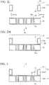
- FIGS.2A to 2M are sectional views showing a method of manufacturing an electronic component package of a first example of the present invention
- FIG.3 and FIG.4 are sectional views showing the electronic component package of the same respectively
- FIG.5 to FIG.7 are sectional views showing an electronic component device of the same respectively.
- a first silicon wafer 10 of a 600 to 800 ⁇ m thickness is prepared as a silicon substrate.
- One or plural package regions are defined on the first silicon wafer 10 to obtain individual packages.
- a mask layer 12 in which opening portions 12x to form the through holes are provided is formed on the first silicon wafer 10.
- the resist may be patterned in a single layer.
- the mask layer 12 may be formed by patterning a resist on a hard mask layer such as a silicon oxide layer, or the like, and then etching the hard mask layer using the resist as a mask.
- through holes TH are formed by etching the first silicon wafer 10 through the opening portions 12x while using the mask layer 12 as a mask, to pass through from an upper surface to a lower surface.
- the through holes TH are formed in the package regions of the first silicon wafer 10 respectively. Then, the mask layer 12 is removed.
- an insulating layer 14 made of a silicon oxide layer and having a film thickness of about 500 nm is formed on both surfaces of the first silicon wafer 10 and inner surfaces of the through holes TH, by thermally oxidizing the first silicon wafer 10.
- a silicon oxide layer formed on the all surfaces of the first silicon wafer 10 by the CVD method may be used as the insulating layer 14.
- the first silicon wafer 10 is arranged on a plating power feeding member 16 such as a copper foil, or the like via an adhesive layer 15. Openings are provided in portions, which correspond to the through holes TH in the first silicon wafer 10, of the adhesive layer 15. Also, a metal (a copper, or the like) is filled from a lower portion to an upper portion of the through hole TH by the electroplating utilizing the plating power feeding member 16 as a plating power feeding path, and thus through electrodes 18 are formed. Then, the plating power feeding member 16 and the adhesive layer 15 are removed from the first silicon wafer 10.
- a plating power feeding member 16 such as a copper foil, or the like via an adhesive layer 15. Openings are provided in portions, which correspond to the through holes TH in the first silicon wafer 10, of the adhesive layer 15.
- a metal a copper, or the like
- the through electrodes 18 are formed in a state that projection portions P protrude upward from the upper surface of the insulating layer 14 on the first silicon wafer 10.
- heights of the projection portions P of the through electrodes 18 are varied due to an in-plane variation of the electroplating.
- the through electrodes 18 are formed in a state that the projection portions P protrude downward.
- the projection portions P of the through electrodes 18 on both surface sides of the first silicon wafer 10 are polished by the CMP (Chemical Mechanical Polishing), or the like respectively.
- the upper surfaces of the through electrodes 18 are made equal in height to the insulating layer 14 on both surface sides of the first silicon wafer 10, so that the whole surface is planarized. That is, the upper surfaces and the lower surfaces of the through electrodes 18 and the surfaces of the insulating layer 14 on both surface sides constitute an identical surface respectively and they are planarized.
- An upper surface of through electrode 10 constitutes a connection portion 18a.
- the through electrodes 18 are formed in the first silicon wafer 10 to which no cavity is provided and which is flat over the whole area. Therefore, unlike the prior art, the through electrodes 18 can be easily planarized. As a result, the coplanarity of connection portions 18a of the through electrodes 18 can be improved, and the electronic component can be mounted with good reliability.
- FIG.2H a second silicon wafer 20 similar to the first silicon wafer 10 is prepared.
- the insulating layer 14 made of a silicon oxide layer is formed on both surfaces of the second silicon wafer 20 and inner surfaces of the through portions TP by thermally oxidizing the second silicon wafer 20.
- the grid-like frame portion 22 is constructed from the silicon portion 20a and the insulating layer 14 for coating the silicon portion 20a.
- the grid-like frame portion 22 may be formed only of the silicon portion 20a by omitting the insulating layer 14.
- the grid-like frame portion 22 provided to the second silicon wafer 20 is formed to correspond to the boundary portion of the package regions R of the first silicon wafer 10 (a plan view of FIG.2G ) respectively. In this manner, the second silicon wafer 20 is processed and becomes the frame member.
- the second silicon wafer 20 in which the grid-like frame portion 22 is provided is adhered onto the foregoing first silicon wafer 10 in which the through electrodes 18 are provided in the package regions R in FIG.2G .
- an ultrasonic wave is applied to the first and second silicon wafers 10, 20 for 5 minute in a state that these wafers are dipped in ozone water (ozone concentration: 8 ppm).
- the ultrasonic wave is applied to the first and second silicon wafers 10, 20 for 5 minute in a state that these wafers are dipped in water. Then, the first and second silicon wafers 10, 20 are dried by a spin driver. Accordingly, an organic substance, etc. adhered to surfaces of the first and second silicon wafers 10, 20 are removed and rinsed out.
- a first plasma process is applied to respective joining surfaces of the first and second silicon wafers 10, 20 by using an oxygen (O 2 ) gas.
- an oxygen (O 2 ) gas As an example of the conditions of the first plasma process, a pressure: 55 Pa, a high-frequency power (13.56 MHz): 70 W, and a processing time: 30 second are employed.
- a second plasma process is applied to respective joining surfaces of the first and second silicon wafers 10, 20 by using a nitrogen (N 2 ) gas.
- N 2 nitrogen
- a processing time: 15 second are employed.
- respective joining surfaces of the first and second silicon wafers 10, 20 are hydrophilized, and surface conditions suitable for the joining can be obtained.
- the second silicon wafer 20 is aligned with the first silicon wafer 10 and arranged such that the grid-like frame portion 22 of the second silicon wafer 20 corresponds to the boundary portion of respective package regions R of the first silicon wafer 10 (see plan views of FIG.2G and FIG.2K ).
- the first and second silicon wafers 10, 20 being stacked are press-bonded by applying a pressure of 100 N/wafer to both wafers for 5 second. Then, the heat treatment is applied to the first and second silicon wafers 10, 20 at a temperature of 150 °C for 8 hour. Thus, as shown in FIG.2M , the grid-like frame portion 22 of the second silicon wafer 20 is joined onto the first silicon wafer 10.
- a temperature of the heat treatment can be set freely between 100 to 400 °C. That is, by performing the plasma process to the first and second silicon wafers 10, 20, both wafers can be joined at a low temperature at a heatproof temperature or less of the through electrode 18.
- the grid-like frame portion 22 of the second silicon wafer 20 is arranged on the boundary portion of respective package regions R of the first silicon wafer 10, thereby the cavity C is provided in the center portions of the package regions R respectively.
- a wafer-like package member 3 having such a structure that the grid-like frame portion 22 is provided upright on the peripheral portions of the package regions R of the first silicon wafer 10 respectively can be obtained.
- the grid-like frame portion 22 is made of silicon.
- any material may be employed if such material can be joined to the first silicon wafer 10 by the above-mentioned bonding method.
- the electronic component may be mounted on the package regions R of the wafer-like package member 3 respectively, and then the electronic component device may be constructed by cutting the first and second silicon wafers 10, 20. Alternately, individual electronic component packages may be obtained by cutting the first and second silicon wafers 20, and then the electronic component device may be constructed by mounting the electronic component.
- FIG.3 an electronic component package 1 of the present example obtained when the package member 3 in FIG.2M is cut is shown.
- the first and second silicon wafers 10, 20 are cut, the first silicon wafer 10 becomes individual silicon substrates 10a, and the grid-like frame portion 22 of the second silicon wafer 20 becomes individual frame portions 23.
- the electronic component package 1 of the first example is constructed basically by a package substrate portion 11 and the frame portion 23 joined to the peripheral portion thereof to stand upright.
- the through holes TH are provided in the silicon substrate 10a, and the insulating layer 14 is formed on both surface sides of the silicon substrate 10a and the inner surfaces of the through holes TH.
- the through electrodes 18 are provided in the through holes TH, and upper surfaces and lower surfaces of the through electrodes 18 are planarized at the same height as the surfaces of the insulating layer 14 on both surface sides of the silicon substrate 10a respectively.
- the frame portion 23 is constructed by coating the upper surface and the lower surface and the inner surface sides of the silicon portion 20a with the insulating layer 14. Then, the insulating layer 14 on the lower surface side of the frame portion 23 is joined to the insulating layer 14 on the upper surface side of the package substrate portion 11. Thus, the cavity C is provided in the center major portion on the package substrate portion 11.
- the through electrodes 18 are formed on the first silicon wafer 10, in which the cavity C is not provided and which is made flat, via the insulating layer 14, and then the projection portions P of the through electrodes 18 are planarized by the polishing. Then, the second silicon wafer 20 in which the grid-like frame portion 22 is provided is joined onto the first silicon wafer 10. Thus, the cavity C is provided in the package regions R of the first silicon wafer 10 respectively.
- the joining of the first silicon wafer 10 and the second silicon wafer 20 is carried out by rinsing out respective joining surfaces, applying the plasma process them, aligning them with each other and press-bonding them, and applying the heat treatment to them at the low temperature side (150 °C).
- the method of joining the silicon wafers of the present example has been made in view of such problem.
- the second silicon wafer 20 can be joined onto the first silicon wafer 10 by the low temperature process (e.g., 150 °C), which does not damage the through electrodes 18, even in a situation that the through electrodes 18 are provided in the first silicon wafer 10.
- the electronic component package 1 having such a structure that the cavity C is provided on the package substrate portion 11 by the frame portion 23 and also the through electrodes 18 whose coplanarity is good are provided on the package substrate portion 11 in the cavity C can be manufactured easily.
- the insulating layer 14 is omitted from the frame portion 23 of the electronic component package 1 in FIG. 3 may be omitted, and then the cavity C may be constructed by joining the frame portion 23 consisting only of the silicon portion 20a onto the package substrate portion 11.
- the second silicon wafer 20 on which the frame portion 23 consisting only of the silicon portion 20a is provided is joined onto the first silicon wafer 10 by the similar joining method.
- an electronic component device constructed by utilizing the electronic component package 1 of the present example will be explained hereunder.
- bumps 30a of an LED (Light Emitting Diode) 30 are flip-chip connected to the connection portions 18a of the through electrodes 18 in the cavity C of the electronic component package 1 in FIG.3 .
- the LED 30 is housed in the cavity C.
- a fluorescent substance 32 is filled in the cavity C, and the LED 30 is embedded in the fluorescent substance 32.
- external connection terminals 26 are provided by mounting solder balls, or the like under the through electrodes 18.
- the fluorescent substance 32 having a uniform film thickness can be formed easily on the upper surface (light emitting surface) side of the LED 30.
- the LED 30 emits a blue or purple light, for example, and a white light is emitted to the outside by the action of the fluorescent substance 32.
- a transparent cap member may also be provided on the fluorescent substance 32.
- a second electronic component device 2a of the first example is shown.
- bumps 40a of an electronic component 40 are flip-chip connected to the connection portions 18a of the through electrodes 18 in the cavity C of the electronic component package 1a ( FIG.4 ) according to the above variation.
- the electronic component 40 the optical semiconductor element such as LED, or the like, or the MEMS element such as an accelerator sensor, or the like is used.
- a cap member 24 is joined onto the frame portion 23 of the electronic component package 1a.
- a housing portion S is constructed by the package substrate portion 11 and the frame portion 23, and the electronic component 40 is housed in this housing portion S in a hermetically sealed manner.
- the external connection terminals 26 are provided by mounting the solder ball, or the like under the through electrodes 18.
- the electronic component 40 is formed of the optical semiconductor element.
- the cap member 24 is formed of a transparent glass cap, and the glass cap is joined to the frame portion 23 (the silicon portion 20a) of the electronic component package 1a by the anode connecting.
- the optical semiconductor element emits a light to the outside via the glass cap or receives a light from the outside.
- the glass cap can be anode-connected to the frame portion 23.
- the cap member 24 is formed of an opaque material such as a silicon cap in addition to the glass cap.
- the silicon cap is joined to the frame portion 23 of the electronic component package 1a by the joining method utilizing the above-mentioned plasma process.
- the electronic component package 1 having the frame portion 23 whose surface is coated with the insulating layer 14, as shown in FIG.3 may be employed.
- FIG.7 a third electronic component device 2b of the first example is shown.
- the frame portion 23 in the electronic component package 1 in FIG.3 is omitted.
- the bumps 40a of the electronic component 40 are flip-chip connected to the connection portions 18a of the through electrodes 18 of the package substrate portion 11.
- the cap member 24 having such a structure that the cavity C (the recess portion) is provided in the center portion and a projection-like bonding portion 24a is provided in the peripheral portion, is arranged on the package substrate portion 11 such that the cavity C is directed downward. A top end surface of the projection-like bonding portion 24a of the cap member 24 is adhered onto the package substrate portion 11.
- the housing portion S is constructed by the cavity C of the cap member 24, and the electronic component 40 is housed in the housing portion S in a hermetically sealed condition.
- FIG.7 a mode in which the electronic component 40 is formed of the optical semiconductor element is illustrated.
- the cap member 24 is formed of the transparent glass cap, the insulating layer 14 on the peripheral portion of the package substrate portion 11 is partially removed, and the glass cap is anode-connected to the exposed silicon substrate 10.
- the cap member 24 may be formed of the opaque material such as a silicon cap, or the like in addition to the glass cap. In such case, the joining portion of the package substrate portion 11 may be coated with the insulating layer 14.
- the package substrate portion 11 is formed by processing the first silicon wafer 10 that can be processed with high precision. Therefore, the through electrodes 18 can be easily formed at a narrow pitch. Also, the cavity is not formed into the first silicon wafer 10, but the cavity C (housing portion) is constructed by the frame portion 23 and the cap member 24.
- the first silicon wafer 10 is made flat over the whole surface. Therefore, the through electrodes 18 can be easily planarized, and the coplanarity of the connection portion 18a can be set in a good condition. As a result, the high-performance electronic component having a large number of terminals at a narrow pitch can be mounted with good reliability.
- fine wiring pattern layers connected to the through electrodes 18 can be formed after the through electrodes 18 are planarized (after the step in FIG.2G ).
- the electronic component package of the present example can respond to the mounting of various electronic components, and a margin of design can be widened.
- FIGS.8A to 8F are sectional views showing a method of manufacturing an electronic component package of a second example of the present invention
- FIG.9 is a sectional view showing an electronic component device of the same.
- a feature of the second example resides in that elements (diodes, and the like) connected to the electronic component are formed into the silicon substrate constituting the electronic component package.
- elements diodes, and the like
- detailed explanation about the same elements and the same steps as those in the first example will be omitted.
- the identical structure to the first silicon wafer 10 in FIG.2G is formed by the similar method to the first example, the structure constitutes an upper package member 3a. More particularly, the through holes TH are formed in the first silicon wafer 10, then the insulating layer 14 is formed on the whole surface, then the through electrodes 18 are formed in the through holes TH, and then both surface sides of the first silicon wafer 10 are planarized.
- the second silicon wafer 20 into the upper surface side of which Zener diodes ZD are formed is prepared.
- the Zener diode ZD is formed by ion-implanting a p-type conductive impurity (a boron, or the like) into the n-type second silicon wafer 20.
- a first insulating layer 50 in which opening portions are provided on the Zener diodes ZD is formed on the second silicon wafer 20.
- electrode pads 52 each connected to the Zener diode ZD are formed on the first insulating layer 50.
- the electrode pad 52 is constructed by forming a Ti(titanium) layer/a TiN (titanium nitride) layer/an Al (aluminum) layer in order from the bottom.
- a second insulating layer 54 in which opening portions 54x are provided on the electrode pads 52 is formed on the first insulating layer 50. Also, an insulating layer 51 is formed on the lower surface of the second silicon wafer 20.
- a metal layer 56a is obtained by forming a Ti layer/a Cu (copper) layer sequentially from the bottom on the second insulating layer 54 and the electrode pads 52 by the sputter method. Then, the metal layer 56a is polished by the CMP, or the like until the second insulating layer 54 is exposed. Accordingly, as shown in FIG.8D , the metal layer 56a is embedded in the opening portions 54x in the second insulating layer 54, and thus connection electrodes 56 connected to the electrode pads 52 are obtained. In this manner, the connection electrodes 56 connected electrically to the Zener diode ZD respectively are provided on the upper surface side of the second silicon wafer 20 in their exposed state. Then, the second silicon wafer 20 in FIG.8D constitutes a lower package member 3b.
- connection portion 18a (the copper layer) of the through electrode 18 in the upper package member 3a in FIG.8A above mentioned are joined to the connection electrodes 56 (the copper layer) of the lower package member 3b in FIG.8D .
- this joining method the similar method to the step in FIG.2L in the first example is employed. In other words, respective joining surfaces of the upper package member 3a and the lower package member 3b are rinsed out, then the plasma process is applied to the upper and lower package member 3a, 3b, then the upper and lower package member 3a, 3b are aligned with each other and then press-bonded, and then the heat treatment is applied to the upper and lower package member 3a, 3b at a temperature of 150 °C.
- the method of joining with the lower temperature side by utilizing the plasma process can be applied not only to join the silicon and the silicon, the silicon and the silicon oxide layer (the insulating layer), or the silicon oxide layer and the silicon oxide layer (the insulating layer) but also to join various metal materials such as the copper and the copper, and the like.
- connection electrodes 56 of the lower package member 3b and the connection portions 18a of the through electrodes 18 of the upper package member 3a are joined and connected electrically mutually.
- Zener diodes ZD provided to the lower package member 3b are connected electrically to the through electrodes 18 of the upper package member 3a via the electrode pads 52 and the connection electrodes 56.
- the package member 3 of the second example that is constructed by stacking the upper package member 3a on the lower package member 3b is obtained.
- the electronic component may be mounted on the package regions of the wafer-like package member 3 respectively, and then individual electronic component devices may be constructed by cutting the package member 3. Alternately, individual electronic component packages may be obtained by cutting the package member 3, and then the electronic component device may be constructed by mounting the electronic component.
- FIG.9 the electronic component device constructed by using the electronic component package of the second example is shown.
- an electronic component package 1b of an electronic component device 2c of the second example is obtained by cutting the package member 3 in FIG.8F , and is basically constructed by stacking an upper package portion 4a on a lower package portion 4b.
- the Zener diodes ZD are formed on the upper surface side of the silicon substrate 20a, and the Zener diodes ZD are connected to the connection electrodes 56 via the electrode pads 52.
- the insulating layer 14 is formed on both surface sides of the silicon substrate 10a and the inner surfaces of the through holes TH provided in this substrate, and the through electrodes 18 both surface sides of which are planarized are filled in the through holes TH.
- connection portions 18a of the through electrodes 18 in the upper package portion 4a are joined to the connection electrodes 56 on the upper surface side of the lower package portion 4b.
- the bumps 30a of the LED 30 are flip-chip connected to the upper connection portions 18a of the through electrodes 18 in the upper package portion 4a. Also, the LED 30 is embedded in the fluorescent substance 32, and the upper surface (the light emitting surface) of the LED 30 is covered with the fluorescent substance 32. Like the electronic component package 1 in FIG.5 in the first example, the LED 30 emits a blue or purple light, for example, and a white light is emitted to the outside by the action of the fluorescent substance 32.
- the LED 30 is connected to the Zener diodes ZD, which are provided in the silicon substrate 20a of the lower package portion 4b, via the through electrodes 18 of the upper package portion 4a and the connection electrodes 56 and the electrode pads 52 of the lower package portion 4b.
- the Zener diode ZD is connected electrically in parallel with the LED 30 in a power supply line and functions as a power supply regulator.
- the cap member 24 made of a transparent glass and having such a structure that the cavity C is provided in the center portion and the projection-like bonding portion 24a is provided on the peripheral portion, is arranged and joined onto the electronic component package 1b of the second example.
- the insulating layer 14 on the peripheral portion of the upper package portion 4a is partially removed, and the cap member 24 is anode-connected to the silicon substrate 10a of the upper package portion 4a.
- the LED 30 mounted on the upper package portion 4a is housed in the housing portion S constructed by the cap member 24 in a hermetically sealed condition.
- the LED 30 may be embedded in the fluorescent substance 32, and then the transparent cap member may be provided thereon.
- the Zener diodes ZD connected to the LED 30 are built in the silicon substrate 20a of the lower package portion 4b.
- the MEMS element such as an acceleration sensor, or the like may be mounted instead of the LED 30 on the upper package portion 4a, and the semiconductor element for driving the MEMS element, or the like may be built in the silicon substrate 20a of the lower package portion 4b. That is, each of various electronic components can be mounted on the upper package portion 4a, and various elements (semiconductor element, diode, capacitor, resistor, inductor, and the like) connected to the electronic component can be built in the silicon substrate 20a of the lower package portion 4b.
- the electronic component device 2d having the cap member 24 in FIG.10 is employed, and then the MEMS element is hermetically sealed in the housing portion S.
- the opaque material such as the silicon cap, or the like in addition to the transparent glass can be employed as the cap member 24.
- the through electrodes 18 provided to the upper package portion 4a can be formed at a narrow pitch and the upper and lower connection portions 18a are planarized. Therefore, the electronic component package of the present example is applicable to the package in which the high-performance electronic component is mounted.
- the Zener diode ZD must be covered with a protection layer to prevent an adhesion of the foreign substance after these diodes are formed, or a degree of clean of the process environment must be set highly. As a result, such a problem existed that the process management becomes complicated.
- the Zener diodes ZD are not formed in the upper package portion 4a in which the through electrodes 18 are provided, but the Zener diodes ZD are provided to the lower package portion 4b and then the Zener diodes ZD are connected to the through electrodes 18 in the upper package portion 4a by the joining method on the low-temperature side using the plasma process.
- FIGS.11A to 11D are sectional views showing a method of manufacturing an electronic component package of an embodiment of the present invention
- FIG.12 is a sectional view showing the electronic component package of the same
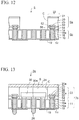
- FIG.13 is a sectional view showing the electronic component device of the same.
- a feature of the embodiment resides in that, in the second example, the grid-like frame portion is formed in the second silicon wafer in which the Zener diodes are formed and then this second silicon wafer is joined onto the first silicon wafer in which the through electrodes are provided, whereby the electronic component package in which the cavity is provided is manufactured.
- the grid-like frame portion is formed in the second silicon wafer in which the Zener diodes are formed and then this second silicon wafer is joined onto the first silicon wafer in which the through electrodes are provided, whereby the electronic component package in which the cavity is provided is manufactured.
- the same structure as the lower package member 3b shown in FIG.8D in the second example is formed, and the structure constitutes an upper package member 5a.
- the mask layer 12 in which an opening portion 12z is provided in a major center portion of each package region of the upper package member 5a is formed.
- the upper package member 5a that is turned upside down from FIG.11C is arranged on the lower package member 5b, and the connection electrodes 56 of the grid-like frame portion 22 in the upper package member 5a are joined to the connection portions 18a of respective through electrodes 18 in the lower package member 5b.
- the joining method the method of utilizing the plasma process as in the first and second examples may be employed.
- connection electrodes 56 of the upper package member 5a are joined and connected electrically to the upper connection portions 18a of respective through electrodes 18 in lower package member 5b.
- the cavity C constructed by the grid-like frame portion 22 is provided in each package region of the lower package member 5b. Accordingly, a package member 5 of the embodiment is obtained.
- the electronic component may be mounted on the wafer-like package member 5, and then individual electronic component devices may be constructed by cutting the grid-like frame portion 22 and the lower package member 5b. Alternately, individual packages may be obtained by cutting the grid-like frame portion 22 and the lower package member 5b, and then the electronic component devices may be constructed by mounting the electronic component respectively.
- FIG.13 an electronic component device constructed by using the electronic component package of the embodiment is shown.
- an electronic component package 1c of an electronic component device 2e of the embodiment is obtained by cutting the above package member 5 in FIG.12 , and is basically constructed by the package substrate portion 11 and the frame portion 23 provided upright on the peripheral portion.
- the through holes TH are provided in the silicon substrate 10a, and the insulating layer 14 is formed on both surface sides of the silicon substrate 10a and the inner surfaces of the through holes TH.
- the through electrodes 18 are provided in the through holes TH, and the upper surfaces and the lower surface of the through electrodes 18 are planarized at the same height as the upper surface and the lower surface of the insulating layer 14 on the silicon substrate 10a respectively.
- the frame portion 23 is joined to the peripheral portion on the package substrate portion 11, and thus the cavity C is provided in the center major portion on the silicon substrate 10a.
- the Zener diodes are formed in the lower surface side of the silicon portion 20a of the frame portion 23, and the connection electrodes 56 connected to the Zener diodes are joined to the upper connection portions 18a of respective through electrodes 18 of the package substrate portion 11.
- wiring pattern layers 19 for connecting the through electrodes 18 mutually are provided on the lower surface side of the silicon substrate 10a of the package substrate portion 11.
- the bumps 30a of the LED 30 are flip-chip connected to the upper connection portions 18a of the through electrodes 18 of the package substrate portion 11.
- the cap member 24 is joined to the frame portion 23, and the LED 30 is housed in the housing portion S in a hermetically sealed condition.
- the external connection terminal 26 connected to the through electrodes 18 are provided on the lower surface of the package substrate portion 11.
- the cap member 24 is formed of a transparent glass cap, the insulating layer 51 on the upper surface of the frame portion 23 is removed at a predetermined stage, and the cap member 24 (the glass cap) is anode-connected to the silicon portion 20a. Otherwise, like the first electronic component device 2 ( FIG.5 ) in the first example, the cap member 24 may be omitted and then the LED 30 may be embedded in the fluorescent substance. Alternately, the LED 30 may be embedded in the fluorescent substance and then the transparent cap member may be further provided thereon.
- the LED 30 is connected to the Zener diodes ZD in the frame portion 23 via the through electrodes 18 to which the bumps 30a are connected, the wiring pattern layers 19 formed on the lower surface and connected to the electrodes, other through electrodes 18 connected to the layers, and others.
- the wiring pattern layers 19 for connecting the through electrodes 18 mutually may be formed on the upper surface side of the package substrate portion 11.
- the embodiment can achieve the similar advantages to those of the second example.
- the frame portion 23 in which the Zener diodes ZD are provided is joined onto the package substrate portion 11 in which the through electrodes 18 having the good coplanarity are provided. Therefore, the electronic component package 1c to which the cavity C is provided and in which the Zener diodes ZD are built can be manufactured easily.
- the LED 30 can be hermetically sealed in the housing portion S by the cap member 24 in a condition that such LED 30 is connected to the through electrodes 18 in the cavity C and the Zener diodes ZD in the frame portion 23 with good reliability.
- the MEMS element, another optical semiconductor element, or the like may be mounted in place of the LED 30.
- the cap member 24 may be formed of the opaque material such as the silicon cap, or the like.
Landscapes
- Engineering & Computer Science (AREA)
- Microelectronics & Electronic Packaging (AREA)
- Manufacturing & Machinery (AREA)
- Led Device Packages (AREA)
- Micromachines (AREA)
- Wire Bonding (AREA)
- Piezo-Electric Or Mechanical Vibrators, Or Delay Or Filter Circuits (AREA)
Claims (5)
- Elektronisches Bauteilpaket, umfassend:einen Paketsubstratabschnitt (11), der durch ein erstes Siliziumsubstrat (10a) erstellt ist, in dem mindestens zwei Durchgangslöcher (TH) vorgesehen sind, eine erste Isolierschicht (14), die auf oberen und unteren Flächenseiten des ersten Siliziumsubstrats (10a) und einer Innenfläche der Durchgangslöcher (TH) gebildet ist, und
erste und zweite Durchgangselektroden (18), die entsprechend in die mindestens zwei Durchgangslöcher (TH) gefüllt sind; undeinen Rahmenabschnitt (23), der aus einem zweiten Siliziumsubstrat (20a) gebildet ist, wobei der Rahmenabschnitt (23) eine Öffnung definiert, die sich von einer oberen Fläche zu einer unteren Fläche des Rahmenabschnitts (23) erstreckt und oben auf einen peripheren Abschnitt des Paketsubstratabschnitts (11) gestapelt ist, um einen Hohlraum (C) auf dem ersten Siliziumsubstrat (10a) zu bilden, wobei sich die erste Elektrode (18) in dem Hohlraum (C) befindet;wobei entsprechende obere Flächen der ersten und zweiten Durchgangselektroden (18) mit einer oberen Fläche der ersten Isolierschicht (14) koplanar sind, die auf der oberen Flächenseite des ersten Siliziumsubstrats (10a) gebildet ist, und entsprechende untere Flächen der ersten und zweiten Durchgangselektroden (18) mit einer unteren Fläche der ersten Isolierschicht (14) koplanar sind, die auf der unteren Flächenseite des ersten Siliziumsubstrats (10a) gebildet ist; und
wobei die erste Isolierschicht (14), die auf der oberen Fläche des ersten Siliziumsubstrats (10a) gebildet ist, direkt in Kontakt mit der oberen Fläche des ersten Siliziumsubstrats (10a) ist und direkt unter dem gesamten Rahmenabschnitt (23) angeordnet ist;
wobei zusätzlich zu dem zweiten Siliziumsubstrat (20a) der Rahmenabschnitt (23) ein Element (ZD) umfasst, das auf einer unteren Flächenseite des zweiten Siliziumsubstrats (20a) gebildet ist, eine Verbindungselektrode (56) unter dem Element (ZD) gebildet und elektrisch mit dem Element (ZD) verbunden ist und eine zweite Isolierschicht (54) auf einem Umfang der Verbindungselektrode (56) gebildet ist;
wobei das Element (ZD) eines von einer Diode, einem Halbleiterelement, einem Kondensator, einem Widerstand und einem Induktor ist und die Verbindungselektrode (56) des Rahmenabschnitts (23) direkt mit der zweiten Durchgangselektrode (18) des Paketsubstratabschnitts (11) verbunden ist und die erste Isolierschicht (14) des Paketsubstratabschnitts (11) direkt die zweite Isolierschicht (54) des Rahmenabschnitts (23) kontaktiert. - Elektronische Bauteilvorrichtung, umfassend:ein elektronisches Bauteilpaket (1c) nach Anspruch 1; undein elektronisches Bauteil (30), das mit einem oberen Verbindungsabschnitt (18a) von Durchgangselektroden (18) verbunden ist, die im ersten Siliziumsubstrat (10a) vorgesehen und innerhalb des Hohlraums (C) positioniert sind.
- Elektronische Bauteilvorrichtung nach Anspruch 2, wobei ein Kappenelement (24), das verwendet wird, um das elektronische Bauteil (30a) hermetisch abzudichten, auf dem elektronischen Bauteilpaket vorgesehen ist.
- Elektronische Bauteilvorrichtung nach Anspruch 3, wobei das elektronische Bauteil (30) eine LED ist und die LED mit einem Leuchtstoff (32) beschichtet ist.
- Verfahren zur Herstellung eines elektronischen Bauteilpakets, das die Schritte umfasst:Bilden eines Paketelements (11) durch ein Verfahren, das einen Schritt des Bildens von mindestens zwei Durchgangslöchern (TH) in einer Paketregion (R) eines ersten Siliziumsubstrats (10a), einen Schritt des Bildens einer ersten Isolierschicht (14) auf oberen und unteren Flächen des ersten Siliziumsubstrats (10a) und einer Innenfläche der Durchgangslöcher (TH), einen Schritt des Füllens erster und zweiter Durchgangselektroden (18) entsprechend in die mindestens zwei Durchgangslöcher (TH) und einen Schritt des Planarisierens der ersten und zweiten Durchgangselektroden (18), sodass entsprechende obere Flächen der ersten und zweiten Durchgangselektroden (18) mit einer oberen Fläche der ersten Isolierschicht (14) koplanar sind, die auf der oberen Flächenseite des ersten Siliziumsubstrats (10a) gebildet ist, und entsprechende untere Flächen der ersten und zweiten Durchgangselektroden (18) mit einer unteren Fläche der ersten Isolierschicht (14) koplanar sind, die auf der unteren Flächenseite des ersten Siliziumsubstrats (10a) durch Polieren der ersten und zweiten Durchgangselektroden (18) gebildet ist, umfasst;Vorbereiten eines Rahmenelements (22), das aus einem zweiten Siliziumsubstrat (20a) gebildet ist und einem peripheren Abschnitt des Paketbereichs (R) des ersten Siliziumsubstrats (10) entspricht, vor oder nach dem Schritt des Bildens des Paketelements (11), wobei das Rahmenelement (22) eine Öffnung definiert, die sich von einer oberen Fläche zu einer unteren Fläche des Rahmenelements (22) erstreckt; und Vorsehen eines Hohlraums (C) auf dem Paketelement (11) durch Verbinden des Rahmenelements (22) mit dem peripheren Abschnitt der Paketregion (R) des Paketelements (11), sodass sich die erste Durchgangselektrode (18) innerhalb des Hohlraums (C) befindet;wobei
die erste Isolierschicht (14), die auf der oberen Fläche des ersten Siliziumsubstrats (10a) gebildet ist, direkt in Kontakt mit der oberen Fläche des ersten Siliziumsubstrats (10a) ist und direkt unter dem gesamten Rahmenelement (22) angeordnet ist,
wobei zusätzlich zu dem zweiten Siliziumsubstrat (20a) das Rahmenelement (22) ein Element (ZD) umfasst, das auf einer unteren Flächenseite des zweiten Siliziumsubstrats (20a) gebildet ist, eine Verbindungselektrode (56), die unter dem Element (ZD) gebildet und elektrisch mit dem Element (ZD) verbunden ist, und eine zweite Isolierschicht (54), die auf einem Umfang der Verbindungselektrode (56) gebildet ist;
wobei das Element (ZD) eines von einer Diode, einem Halbleiterelement, einem Kondensator, einem Widerstand und einem Induktor ist und
im Schritt des Verbindens des Rahmenelements (22) die Verbindungselektrode (56) des Rahmenelements (22) direkt mit der zweiten Durchgangselektrode (18) des Paketelements (11) verbunden ist und die erste Isolierschicht (14) des Paketelements (11) direkt die zweite Isolierschicht (54) des Rahmenelements (22) kontaktiert.
Applications Claiming Priority (2)
| Application Number | Priority Date | Filing Date | Title |
|---|---|---|---|
| JP2007163006A JP5137059B2 (ja) | 2007-06-20 | 2007-06-20 | 電子部品用パッケージ及びその製造方法と電子部品装置 |
| EP08155189.7A EP2017888B1 (de) | 2007-06-20 | 2008-04-25 | Gehäuse für eine elektronische Komponente und Verfahren zu dessen Herstellung sowie elektronisches Bauelement |
Related Parent Applications (3)
| Application Number | Title | Priority Date | Filing Date |
|---|---|---|---|
| EP08155189.7 Division | 2008-04-25 | ||
| EP08155189.7A Division-Into EP2017888B1 (de) | 2007-06-20 | 2008-04-25 | Gehäuse für eine elektronische Komponente und Verfahren zu dessen Herstellung sowie elektronisches Bauelement |
| EP08155189.7A Division EP2017888B1 (de) | 2007-06-20 | 2008-04-25 | Gehäuse für eine elektronische Komponente und Verfahren zu dessen Herstellung sowie elektronisches Bauelement |
Publications (2)
| Publication Number | Publication Date |
|---|---|
| EP2666745A1 EP2666745A1 (de) | 2013-11-27 |
| EP2666745B1 true EP2666745B1 (de) | 2016-12-14 |
Family
ID=40091274
Family Applications (3)
| Application Number | Title | Priority Date | Filing Date |
|---|---|---|---|
| EP08155189.7A Active EP2017888B1 (de) | 2007-06-20 | 2008-04-25 | Gehäuse für eine elektronische Komponente und Verfahren zu dessen Herstellung sowie elektronisches Bauelement |
| EP13152256.7A Active EP2586742B1 (de) | 2007-06-20 | 2008-04-25 | Gehäuse für eine elektronische Komponente und Verfahren zu dessen Herstellung |
| EP13181356.0A Active EP2666745B1 (de) | 2007-06-20 | 2008-04-25 | Gehäuse für eine elektronische Komponente und Verfahren zu dessen Herstellung |
Family Applications Before (2)
| Application Number | Title | Priority Date | Filing Date |
|---|---|---|---|
| EP08155189.7A Active EP2017888B1 (de) | 2007-06-20 | 2008-04-25 | Gehäuse für eine elektronische Komponente und Verfahren zu dessen Herstellung sowie elektronisches Bauelement |
| EP13152256.7A Active EP2586742B1 (de) | 2007-06-20 | 2008-04-25 | Gehäuse für eine elektronische Komponente und Verfahren zu dessen Herstellung |
Country Status (3)
| Country | Link |
|---|---|
| US (1) | US8129830B2 (de) |
| EP (3) | EP2017888B1 (de) |
| JP (1) | JP5137059B2 (de) |
Families Citing this family (27)
| Publication number | Priority date | Publication date | Assignee | Title |
|---|---|---|---|---|
| DE102008005345A1 (de) * | 2007-09-28 | 2009-04-02 | Osram Opto Semiconductors Gmbh | Halbleiterbasiertes Bauelement, Aufnahme für ein halbleiterbasiertes Bauelement und Verfahren zur Herstellung eines halbleiterbasierten Bauelements |
| EP2377826B2 (de) | 2009-01-13 | 2020-05-27 | AGC Inc. | OPTISCHES ELEMENT MIT TiO2-HALTIGEM QUARZGLAS |
| JP5210912B2 (ja) * | 2009-02-04 | 2013-06-12 | 新光電気工業株式会社 | 配線基板、電子装置及び電子装置実装構造 |
| KR101064026B1 (ko) * | 2009-02-17 | 2011-09-08 | 엘지이노텍 주식회사 | 발광 디바이스 패키지 및 그 제조방법 |
| JP5372579B2 (ja) * | 2009-04-10 | 2013-12-18 | 新光電気工業株式会社 | 半導体装置及びその製造方法、並びに電子装置 |
| US9214456B2 (en) | 2009-08-13 | 2015-12-15 | SemiLEDs Optoelectronics Co., Ltd. | Light emitting diode (LED) system having lighting device and wireless control system |
| US8933467B2 (en) * | 2009-08-13 | 2015-01-13 | SemiLEDs Optoelectronics Co., Ltd. | Smart integrated semiconductor light emitting system including nitride based light emitting diodes (LED) and application specific integrated circuits (ASIC) |
| US8368187B2 (en) * | 2010-02-03 | 2013-02-05 | Stats Chippac, Ltd. | Semiconductor device and method of forming air gap adjacent to stress sensitive region of the die |
| US8564114B1 (en) * | 2010-03-23 | 2013-10-22 | Amkor Technology, Inc. | Semiconductor package thermal tape window frame for heat sink attachment |
| US8174108B2 (en) * | 2010-03-24 | 2012-05-08 | Avago Technologies Enterprise IP (Singapore) Pte. Ltd. | Method for facilitating the stacking of integrated circuits having different areas and an integrated circuit package constructed by the method |
| US8552458B2 (en) * | 2010-06-26 | 2013-10-08 | SemiLEDs Optoelectronics Co., Ltd. | Side by side light emitting diode (LED) having separate electrical and heat transfer paths |
| EP2481703B1 (de) * | 2011-01-27 | 2020-07-01 | Sensirion AG | Sensorschutz |
| DE102011004577B4 (de) * | 2011-02-23 | 2023-07-27 | Robert Bosch Gmbh | Bauelementträger, Verfahren zur Herstellung eines solchen Bauelementträgers sowie Bauteil mit einem MEMS-Bauelement auf einem solchen Bauelementträger |
| DE102011012924A1 (de) | 2011-03-03 | 2012-09-06 | Osram Opto Semiconductors Gmbh | Träger für eine optoelektronische Struktur und optoelektronischer Halbleiterchip mit solch einem Träger |
| US8338294B2 (en) * | 2011-03-31 | 2012-12-25 | Soitec | Methods of forming bonded semiconductor structures including two or more processed semiconductor structures carried by a common substrate, and semiconductor structures formed by such methods |
| US20120248621A1 (en) * | 2011-03-31 | 2012-10-04 | S.O.I.Tec Silicon On Insulator Technologies | Methods of forming bonded semiconductor structures, and semiconductor structures formed by such methods |
| US9278849B2 (en) * | 2012-06-15 | 2016-03-08 | The Boeing Company | Micro-sensor package and associated method of assembling the same |
| JP6041731B2 (ja) | 2013-03-27 | 2016-12-14 | 新光電気工業株式会社 | インターポーザ、及び電子部品パッケージ |
| EP2871152B1 (de) | 2013-11-06 | 2017-05-24 | Sensirion AG | Sensorvorrichtung |
| EP3001186B1 (de) | 2014-09-26 | 2018-06-06 | Sensirion AG | Sensorchip |
| EP3032227B1 (de) | 2014-12-08 | 2020-10-21 | Sensirion AG | Flusssensorpaket |
| FR3041148A1 (fr) * | 2015-09-14 | 2017-03-17 | Valeo Vision | Source lumineuse led comprenant un circuit electronique |
| US10497846B2 (en) * | 2017-07-11 | 2019-12-03 | Lg Innotek Co., Ltd. | Light emitting device package |
| TWI778103B (zh) * | 2017-07-21 | 2022-09-21 | 大陸商蘇州樂琻半導體有限公司 | 發光裝置封裝 |
| JP6635605B2 (ja) * | 2017-10-11 | 2020-01-29 | 国立研究開発法人理化学研究所 | 電流導入端子並びにそれを備えた圧力保持装置及びx線撮像装置 |
| DE102019107760A1 (de) | 2019-03-26 | 2020-10-01 | OSRAM Opto Semiconductors Gesellschaft mit beschränkter Haftung | Verfahren zur herstellung einer verbindungsstruktur und halbleiterbauelement |
| KR102796767B1 (ko) * | 2019-07-10 | 2025-04-16 | 삼성전자주식회사 | 인터포저를 포함하는 전자 장치 |
Family Cites Families (20)
| Publication number | Priority date | Publication date | Assignee | Title |
|---|---|---|---|---|
| JPH0810738B2 (ja) * | 1993-08-30 | 1996-01-31 | 株式会社日立製作所 | 半導体装置及びその製造方法 |
| JP3920399B2 (ja) * | 1997-04-25 | 2007-05-30 | 株式会社東芝 | マルチチップ半導体装置用チップの位置合わせ方法、およびマルチチップ半導体装置の製造方法・製造装置 |
| GB9710843D0 (en) * | 1997-05-28 | 1997-07-23 | Secr Defence | A thermal detector array |
| JP2001210872A (ja) * | 2000-01-26 | 2001-08-03 | Sanyo Electric Co Ltd | 半導体発光装置及びその製造方法 |
| US6710461B2 (en) * | 2002-06-06 | 2004-03-23 | Lightuning Tech. Inc. | Wafer level packaging of micro electromechanical device |
| JP3904484B2 (ja) * | 2002-06-19 | 2007-04-11 | 新光電気工業株式会社 | シリコン基板のスルーホールプラギング方法 |
| JP2004063756A (ja) * | 2002-07-29 | 2004-02-26 | Fuji Photo Film Co Ltd | 固体撮像装置およびその製造方法 |
| WO2005043314A2 (en) | 2003-10-22 | 2005-05-12 | Peterson Stanley K | Method of selecting and storing airline ticket data |
| US7645681B2 (en) * | 2003-12-02 | 2010-01-12 | Bondtech, Inc. | Bonding method, device produced by this method, and bonding device |
| JP4408713B2 (ja) * | 2004-02-03 | 2010-02-03 | Necエレクトロニクス株式会社 | 半導体装置の製造方法 |
| JP3751625B2 (ja) * | 2004-06-29 | 2006-03-01 | 新光電気工業株式会社 | 貫通電極の製造方法 |
| JP5094118B2 (ja) * | 2004-08-03 | 2012-12-12 | 株式会社トクヤマ | 発光素子収納用パッケージおよび発光素子収納用パッケージの製造方法 |
| JP2006054307A (ja) * | 2004-08-11 | 2006-02-23 | Shinko Electric Ind Co Ltd | 基板の製造方法 |
| TW200637033A (en) * | 2004-11-22 | 2006-10-16 | Matsushita Electric Industrial Co Ltd | Light-emitting device, light-emitting module, display unit, lighting unit and method for manufacturing light-emitting device |
| KR100593937B1 (ko) * | 2005-03-30 | 2006-06-30 | 삼성전기주식회사 | Si기판을 이용한 LED 패키지 및 그 제조방법 |
| JP4837328B2 (ja) * | 2005-08-01 | 2011-12-14 | 新光電気工業株式会社 | 半導体装置及び半導体装置の製造方法 |
| JP4889974B2 (ja) * | 2005-08-01 | 2012-03-07 | 新光電気工業株式会社 | 電子部品実装構造体及びその製造方法 |
| JP2007067326A (ja) * | 2005-09-02 | 2007-03-15 | Shinko Electric Ind Co Ltd | 発光ダイオード及びその製造方法 |
| JP2007188976A (ja) * | 2006-01-11 | 2007-07-26 | Shinko Electric Ind Co Ltd | 発光装置の製造方法 |
| JP4749870B2 (ja) * | 2006-01-24 | 2011-08-17 | 新光電気工業株式会社 | 発光装置の製造方法 |
-
2007
- 2007-06-20 JP JP2007163006A patent/JP5137059B2/ja active Active
-
2008
- 2008-04-25 EP EP08155189.7A patent/EP2017888B1/de active Active
- 2008-04-25 EP EP13152256.7A patent/EP2586742B1/de active Active
- 2008-04-25 EP EP13181356.0A patent/EP2666745B1/de active Active
- 2008-05-01 US US12/113,393 patent/US8129830B2/en active Active
Non-Patent Citations (1)
| Title |
|---|
| None * |
Also Published As
| Publication number | Publication date |
|---|---|
| JP5137059B2 (ja) | 2013-02-06 |
| EP2017888B1 (de) | 2014-03-05 |
| EP2017888A3 (de) | 2012-07-18 |
| EP2017888A2 (de) | 2009-01-21 |
| JP2009004507A (ja) | 2009-01-08 |
| EP2666745A1 (de) | 2013-11-27 |
| US8129830B2 (en) | 2012-03-06 |
| EP2586742B1 (de) | 2016-05-18 |
| EP2586742A1 (de) | 2013-05-01 |
| US20080315230A1 (en) | 2008-12-25 |
Similar Documents
| Publication | Publication Date | Title |
|---|---|---|
| EP2666745B1 (de) | Gehäuse für eine elektronische Komponente und Verfahren zu dessen Herstellung | |
| US8129833B2 (en) | Stacked integrated circuit packages that include monolithic conductive vias | |
| EP1662564B1 (de) | Halbleiterpaket und herstellungsverfahren dafür | |
| TWI593055B (zh) | 封裝結構及封裝方法 | |
| US8759154B2 (en) | TCE compensation for package substrates for reduced die warpage assembly | |
| US6822324B2 (en) | Wafer-level package with a cavity and fabricating method thereof | |
| JP3186941B2 (ja) | 半導体チップおよびマルチチップ半導体モジュール | |
| US20180145236A1 (en) | Package structure for light emitting device | |
| US20100001305A1 (en) | Semiconductor devices and fabrication methods thereof | |
| JP2009181981A (ja) | 半導体装置の製造方法および半導体装置 | |
| KR20090100895A (ko) | 반도체 패키지 제조 방법 | |
| JP2004153130A (ja) | 半導体装置及びその製造方法 | |
| TW202008043A (zh) | 陣列基板及其製造方法,及應用此陣列基板的顯示裝置及其製造方法 | |
| US20090242923A1 (en) | Hermetically Sealed Device with Transparent Window and Method of Manufacturing Same | |
| US20080079134A1 (en) | Chip package, chip structure and manufacturing process thereof | |
| US8614488B2 (en) | Chip package and method for forming the same | |
| JP2008270362A (ja) | 積層配線基板及びその製造方法 | |
| JP5238182B2 (ja) | 積層配線基板の製造方法 | |
| TW202034410A (zh) | 封裝結構及其製造方法、與電子裝置 | |
| WO2011021364A1 (ja) | 半導体装置およびその製造方法 | |
| JP2012216868A (ja) | 電子部品用パッケージ及び電子部品装置 | |
| JP2004363319A (ja) | 実装基板及び半導体装置 | |
| JP2001102516A (ja) | 半導体装置およびその製造方法 | |
| KR100744700B1 (ko) | 반도체장치 | |
| US20240145255A1 (en) | Electronic device |
Legal Events
| Date | Code | Title | Description |
|---|---|---|---|
| PUAI | Public reference made under article 153(3) epc to a published international application that has entered the european phase |
Free format text: ORIGINAL CODE: 0009012 |
|
| AC | Divisional application: reference to earlier application |
Ref document number: 2017888 Country of ref document: EP Kind code of ref document: P |
|
| AK | Designated contracting states |
Kind code of ref document: A1 Designated state(s): DE |
|
| 17P | Request for examination filed |
Effective date: 20140115 |
|
| RBV | Designated contracting states (corrected) |
Designated state(s): DE |
|
| 17Q | First examination report despatched |
Effective date: 20140224 |
|
| GRAP | Despatch of communication of intention to grant a patent |
Free format text: ORIGINAL CODE: EPIDOSNIGR1 |
|
| RIC1 | Information provided on ipc code assigned before grant |
Ipc: H01L 23/48 20060101ALI20160614BHEP Ipc: H01L 33/62 20100101ALI20160614BHEP Ipc: H01L 33/48 20100101ALI20160614BHEP Ipc: B81C 1/00 20060101AFI20160614BHEP Ipc: H01L 23/045 20060101ALI20160614BHEP |
|
| INTG | Intention to grant announced |
Effective date: 20160708 |
|
| RIN1 | Information on inventor provided before grant (corrected) |
Inventor name: MURAYAMA, KEI |
|
| GRAS | Grant fee paid |
Free format text: ORIGINAL CODE: EPIDOSNIGR3 |
|
| GRAA | (expected) grant |
Free format text: ORIGINAL CODE: 0009210 |
|
| AC | Divisional application: reference to earlier application |
Ref document number: 2017888 Country of ref document: EP Kind code of ref document: P |
|
| AK | Designated contracting states |
Kind code of ref document: B1 Designated state(s): DE |
|
| REG | Reference to a national code |
Ref country code: DE Ref legal event code: R096 Ref document number: 602008047941 Country of ref document: DE |
|
| REG | Reference to a national code |
Ref country code: DE Ref legal event code: R097 Ref document number: 602008047941 Country of ref document: DE |
|
| PLBE | No opposition filed within time limit |
Free format text: ORIGINAL CODE: 0009261 |
|
| STAA | Information on the status of an ep patent application or granted ep patent |
Free format text: STATUS: NO OPPOSITION FILED WITHIN TIME LIMIT |
|
| 26N | No opposition filed |
Effective date: 20170915 |
|
| REG | Reference to a national code |
Ref country code: DE Ref legal event code: R082 Ref document number: 602008047941 Country of ref document: DE Representative=s name: HL KEMPNER PATENTANWAELTE, SOLICITORS (ENGLAND, DE Ref country code: DE Ref legal event code: R082 Ref document number: 602008047941 Country of ref document: DE Representative=s name: HL KEMPNER PATENTANWALT, RECHTSANWALT, SOLICIT, DE Ref country code: DE Ref legal event code: R082 Ref document number: 602008047941 Country of ref document: DE Representative=s name: HL KEMPNER PARTG MBB, DE |
|
| PGFP | Annual fee paid to national office [announced via postgrant information from national office to epo] |
Ref country code: DE Payment date: 20250305 Year of fee payment: 18 |