EP2685154A1 - Lichtquellenmodul - Google Patents
Lichtquellenmodul Download PDFInfo
- Publication number
- EP2685154A1 EP2685154A1 EP12754713.1A EP12754713A EP2685154A1 EP 2685154 A1 EP2685154 A1 EP 2685154A1 EP 12754713 A EP12754713 A EP 12754713A EP 2685154 A1 EP2685154 A1 EP 2685154A1
- Authority
- EP
- European Patent Office
- Prior art keywords
- light source
- electrically
- source module
- conductive
- circuit board
- Prior art date
- Legal status (The legal status is an assumption and is not a legal conclusion. Google has not performed a legal analysis and makes no representation as to the accuracy of the status listed.)
- Withdrawn
Links
- 239000004065 semiconductor Substances 0.000 claims abstract description 40
- 239000012777 electrically insulating material Substances 0.000 claims abstract description 11
- 230000002093 peripheral effect Effects 0.000 claims description 6
- 239000004020 conductor Substances 0.000 claims description 5
- 229920005989 resin Polymers 0.000 description 32
- 239000011347 resin Substances 0.000 description 32
- 239000000463 material Substances 0.000 description 10
- 230000003287 optical effect Effects 0.000 description 6
- 238000012986 modification Methods 0.000 description 5
- 230000004048 modification Effects 0.000 description 5
- 238000003780 insertion Methods 0.000 description 3
- 230000037431 insertion Effects 0.000 description 3
- 238000000465 moulding Methods 0.000 description 2
- 230000000149 penetrating effect Effects 0.000 description 2
- 229920001296 polysiloxane Polymers 0.000 description 2
- RYGMFSIKBFXOCR-UHFFFAOYSA-N Copper Chemical compound [Cu] RYGMFSIKBFXOCR-UHFFFAOYSA-N 0.000 description 1
- 239000004677 Nylon Substances 0.000 description 1
- 229910052782 aluminium Inorganic materials 0.000 description 1
- XAGFODPZIPBFFR-UHFFFAOYSA-N aluminium Chemical compound [Al] XAGFODPZIPBFFR-UHFFFAOYSA-N 0.000 description 1
- 230000000903 blocking effect Effects 0.000 description 1
- 229910052802 copper Inorganic materials 0.000 description 1
- 239000010949 copper Substances 0.000 description 1
- 230000000694 effects Effects 0.000 description 1
- 239000003822 epoxy resin Substances 0.000 description 1
- 230000017525 heat dissipation Effects 0.000 description 1
- 238000005286 illumination Methods 0.000 description 1
- 230000001678 irradiating effect Effects 0.000 description 1
- 229910052751 metal Inorganic materials 0.000 description 1
- 239000002184 metal Substances 0.000 description 1
- 229920001778 nylon Polymers 0.000 description 1
- 238000007747 plating Methods 0.000 description 1
- 229920000647 polyepoxide Polymers 0.000 description 1
Images




Classifications
-
- F—MECHANICAL ENGINEERING; LIGHTING; HEATING; WEAPONS; BLASTING
- F21—LIGHTING
- F21S—NON-PORTABLE LIGHTING DEVICES; SYSTEMS THEREOF; VEHICLE LIGHTING DEVICES SPECIALLY ADAPTED FOR VEHICLE EXTERIORS
- F21S45/00—Arrangements within vehicle lighting devices specially adapted for vehicle exteriors, for purposes other than emission or distribution of light
- F21S45/40—Cooling of lighting devices
- F21S45/47—Passive cooling, e.g. using fins, thermal conductive elements or openings
-
- F—MECHANICAL ENGINEERING; LIGHTING; HEATING; WEAPONS; BLASTING
- F21—LIGHTING
- F21S—NON-PORTABLE LIGHTING DEVICES; SYSTEMS THEREOF; VEHICLE LIGHTING DEVICES SPECIALLY ADAPTED FOR VEHICLE EXTERIORS
- F21S41/00—Illuminating devices specially adapted for vehicle exteriors, e.g. headlamps
- F21S41/10—Illuminating devices specially adapted for vehicle exteriors, e.g. headlamps characterised by the light source
- F21S41/14—Illuminating devices specially adapted for vehicle exteriors, e.g. headlamps characterised by the light source characterised by the type of light source
- F21S41/141—Light emitting diodes [LED]
- F21S41/147—Light emitting diodes [LED] the main emission direction of the LED being angled to the optical axis of the illuminating device
- F21S41/148—Light emitting diodes [LED] the main emission direction of the LED being angled to the optical axis of the illuminating device the main emission direction of the LED being perpendicular to the optical axis
-
- F—MECHANICAL ENGINEERING; LIGHTING; HEATING; WEAPONS; BLASTING
- F21—LIGHTING
- F21S—NON-PORTABLE LIGHTING DEVICES; SYSTEMS THEREOF; VEHICLE LIGHTING DEVICES SPECIALLY ADAPTED FOR VEHICLE EXTERIORS
- F21S41/00—Illuminating devices specially adapted for vehicle exteriors, e.g. headlamps
- F21S41/10—Illuminating devices specially adapted for vehicle exteriors, e.g. headlamps characterised by the light source
- F21S41/19—Attachment of light sources or lamp holders
- F21S41/192—Details of lamp holders, terminals or connectors
-
- F—MECHANICAL ENGINEERING; LIGHTING; HEATING; WEAPONS; BLASTING
- F21—LIGHTING
- F21V—FUNCTIONAL FEATURES OR DETAILS OF LIGHTING DEVICES OR SYSTEMS THEREOF; STRUCTURAL COMBINATIONS OF LIGHTING DEVICES WITH OTHER ARTICLES, NOT OTHERWISE PROVIDED FOR
- F21V19/00—Fastening of light sources or lamp holders
- F21V19/001—Fastening of light sources or lamp holders the light sources being semiconductors devices, e.g. LEDs
- F21V19/003—Fastening of light source holders, e.g. of circuit boards or substrates holding light sources
- F21V19/0055—Fastening of light source holders, e.g. of circuit boards or substrates holding light sources by screwing
-
- F—MECHANICAL ENGINEERING; LIGHTING; HEATING; WEAPONS; BLASTING
- F21—LIGHTING
- F21V—FUNCTIONAL FEATURES OR DETAILS OF LIGHTING DEVICES OR SYSTEMS THEREOF; STRUCTURAL COMBINATIONS OF LIGHTING DEVICES WITH OTHER ARTICLES, NOT OTHERWISE PROVIDED FOR
- F21V29/00—Protecting lighting devices from thermal damage; Cooling or heating arrangements specially adapted for lighting devices or systems
- F21V29/50—Cooling arrangements
- F21V29/70—Cooling arrangements characterised by passive heat-dissipating elements, e.g. heat-sinks
- F21V29/74—Cooling arrangements characterised by passive heat-dissipating elements, e.g. heat-sinks with fins or blades
- F21V29/76—Cooling arrangements characterised by passive heat-dissipating elements, e.g. heat-sinks with fins or blades with essentially identical parallel planar fins or blades, e.g. with comb-like cross-section
- F21V29/763—Cooling arrangements characterised by passive heat-dissipating elements, e.g. heat-sinks with fins or blades with essentially identical parallel planar fins or blades, e.g. with comb-like cross-section the planes containing the fins or blades having the direction of the light emitting axis
-
- H—ELECTRICITY
- H10—SEMICONDUCTOR DEVICES; ELECTRIC SOLID-STATE DEVICES NOT OTHERWISE PROVIDED FOR
- H10H—INORGANIC LIGHT-EMITTING SEMICONDUCTOR DEVICES HAVING POTENTIAL BARRIERS
- H10H20/00—Individual inorganic light-emitting semiconductor devices having potential barriers, e.g. light-emitting diodes [LED]
- H10H20/80—Constructional details
- H10H20/85—Packages
- H10H20/858—Means for heat extraction or cooling
- H10H20/8583—Means for heat extraction or cooling not being in contact with the bodies
-
- F—MECHANICAL ENGINEERING; LIGHTING; HEATING; WEAPONS; BLASTING
- F21—LIGHTING
- F21Y—INDEXING SCHEME ASSOCIATED WITH SUBCLASSES F21K, F21L, F21S and F21V, RELATING TO THE FORM OR THE KIND OF THE LIGHT SOURCES OR OF THE COLOUR OF THE LIGHT EMITTED
- F21Y2115/00—Light-generating elements of semiconductor light sources
- F21Y2115/10—Light-emitting diodes [LED]
Definitions
- the present invention relates to a light source module and, in particular, to a light source module using a semiconductor light emitting device such as an LED as a light source.
- a light source module includes a circuit board placed on a mounting base of a light source holding member and having a surface on which a semiconductor light emitting device is mounted, and a power feeding attachment coupled to a power supply circuit to feeding power to the semiconductor light emitting device.
- a pair of connecting terminals provided in the power feeding attachment is connected to a pair of power feeding pieces formed on the circuit board respectively (see, e.g., Patent Document 1).
- the semiconductor light emitting device For the semiconductor light emitting device to effectively emit light as a light source of a vehicle lamp, it is necessary to prevent luminance from lowering due to heat. Accordingly, a back surface of the circuit board is brought into firm contact with the mounting base of the light source holding member, so that the heat emitted from the semiconductor light emitting device is released to the light source holding member.
- Patent Document 1 JP 2010-192139 A
- an object of the present invention has to do with solving the problem described above, and is to provide a light source module with improved heat release performance while reducing the size of the light source module.
- a light source module including a circuit board having a surface on which a semiconductor light emitting device is mounted, wherein the circuit board is adapted to be placed on a mounting base of a light source holding member, and a power feeding attachment to supply power to the semiconductor light emitting device.
- the circuit board includes a board part on which the semiconductor light emitting device is mounted, and a conductive circuit formed on a surface of the board part, the conductive circuit including a pair of terminal parts and a light source connecting part to connect the pair of terminal parts and the semiconductor light emitting device.
- the power feeding attachment includes an electrically-insulating portion formed of an electrically-insulating material having a higher thermal conductivity than the board part, and a conductive portion formed of a conductive material and embedded in the electrically-insulating portion except a portion thereof.
- the power feeding attachment is adapted to be attached to the light source holding member such that the electrically-insulating portion presses at least a portion of the circuit board against the mounting base.
- the conductive portion may include a pressing tab part protruding from the electrically-insulating portion to press an outer peripheral portion of the circuit board such that the circuit board is pressed against the mounting base.
- a concave portion may be provided in the electrically-insulating portion in a region corresponding to the embedded conductive portion.
- a portion of the conductive portion embedded in the electrically-insulating portion may be exposed to the outside through the concave portion.
- the conductive portion may include a pair of power feeding pieces protruding from the electrically-insulating portion to contact the pair of terminal parts, respectively.
- a light source module including a circuit board having a surface on which a semiconductor light emitting device is mounted, wherein the circuit board is adapted to be placed on a mounting base of a light source holding member, and a power feeding attachment to supply power to the semiconductor light emitting device.
- the circuit board includes a board part on which the semiconductor light emitting device is mounted, and a conductive circuit formed on the surface of the board part, the conductive circuit including a pair of terminal parts and a light source connecting part to connect the pair of terminal parts and the semiconductor light emitting device.
- the power feeding attachment includes an electrically-insulating portion formed of an electrically-insulating material, and a conductive portion formed of a conductive material and embedded in the electrically-insulating portion except a portion thereof.
- the conductive portion includes a pair of power feeding pieces protruding from the electrically-insulating portion to contact the pair of terminal parts, respectively.
- a concave portion is provided in the electrically-insulating portion in a region corresponding to the embedded conductive portion.
- a portion of the conductive portion embedded in the electrically-insulating portion may be exposed to the outside through the concave portion.
- the conductive portion may include a pressing tab part protruding from the electrically-insulating portion to press an outer peripheral portion of the circuit board such that the circuit board is pressed against the mounting base.
- the concave portion may be provided at a position to expose a portion of the conductive portion near the pressing tab part to the outside.
- the electrically-insulating portion may be formed of an electrically-insulating material having a higher thermal conductivity than the board part, and is adapted to be attached to the mounting base such that at least a portion thereof is pressed against the mounting base.
- the conductive portion may include a pair of power feeding pieces protruding from the electrically-insulating portion to contact the pair of terminal parts, respectively.
- a portion (e.g., a back surface) of the circuit board is brought into firm contact with the mounting base of the light source holding member by the electrically-insulating portion of the power feeding attachment, heat generated by the semiconductor light emitting device can be effectively released to the light source holding member.
- a portion of the electrically-insulating portion formed of an electrically-insulating material having a high thermal conductivity is brought into firm contact with the mounting base, so that the heat generated by the semiconductor light emitting device can be released also from the conductive portion contacting the terminal parts of the circuit board at the power feeding pieces and from the electrically-insulating portion pressing the circuit board against the mounting base.
- the light source module can be further downsized without impairing a heat release performance with regard to the heat generated by the semiconductor light emitting device.
- the back surface of the circuit board is brought into firm contact with the mounting base of the light source holding member, so that the heat generated from the semiconductor light emitting device is partially transmitted to the conductive portion of the power feeding attachment from the power feeding parts contacting the terminal parts of the circuit board.
- the concave portion is formed in the electrically-insulating portion in a region corresponding to the conductive portion, so that the thickness is small in the region corresponding to the conductive portion, whereby the heat is effectively dissipated in the air.
- front and rear represents a lamp front-rear direction of the vehicle lamp 1, that is, a direction almost the same as a front-rear direction of a vehicle on which the vehicle lamp 1 is mounted.
- left and right represents a lamp lateral direction of the vehicle lamp 1, that is, a width direction of a vehicle.
- Fig. 1 is a schematic longitudinal sectional view showing the vehicle lamp 1 including the light source module 100 according to the first embodiment of the present invention.
- the vehicle lamp 1 is a vehicle headlamp attached to, for example, a front end portion of a vehicle.
- the vehicle lamp 1 is configured by including a lamp body 12, a transparent cover 14 attached to cover an opening provided at a front end of the lamp body 12, and a lamp unit 20 having a configuration to form a low beam light distribution pattern.
- the lamp unit 20 is a so-called projector-type lamp unit.
- the lamp unit 20 includes a projection lens 21, a reflector 24, a shade 25, the light source module 100, a light source holding member 60, and a support member 70, and is fixed inside a lamp chamber 16 formed by the lamp body 12 and the translucent cover 14.
- An extension 18 is disposed between the lamp unit 20 and the lamp body 12 so as to cover the gap between the lamp body 12 and the lamp unit 20, when viewed from the front of the lamp.
- the projection lens 21 is a plano-convex lens having a spherical convex front surface and a flat rear surface, and is disposed such that a lens optical axis thereof substantially matches a lamp optical axis Ax extending in the front-rear direction of a vehicle.
- the light source module 100 is arranged on a rear side of the projection lens 21, and is positioned and fixed to the light source holding member 60 that is attached to the support member 70.
- the light source module 100 includes a light emitting diode 150, which is a light source of the vehicle lamp 1, and upwardly irradiates light from the light emitting diode 150.
- the reflector 24 is a substantially dome-shaped member disposed above the light source module 100, and a concave surface side thereof is configured as a reflecting surface 24a.
- the reflecting surface 24a is formed in a substantially elliptical spherical shape whose center axis is the lamp optical axis Ax.
- the reflecting surface 24a is designed such that a shape of a cross-section including the lamp optical axis Ax is substantially a portion of an ellipse, and such that eccentricity thereof is gradually increased from a vertical section toward a horizontal section.
- a first focal point of the reflecting surface 24a is substantially at a position where the light emitting diode 150 of the light source module 100 is provided, and a second focal point is substantially at a rear focal point (a position denoted by "F1" in Fig. 1 ) of the projection lens 21.
- light emitted from the light emitting diode 150 of the light source module 100 is forwardly reflected by the reflecting surface 24a of the reflector 24 to converge toward the lamp optical axis Ax" and is projected forward through the projection lens 21, as a light distribution pattern having an inverted image on a focal plane including a rear focal point (F1) of the projection lens 21 (an example of light ray trajectory is denoted by "L1" in Fig. 1 ).
- the shade 25 is configured to form a predetermined cutoff line of the light distribution pattern formed by the light reflected by the reflector 24 by blocking a part of the reflected light, and is disposed between the projection lens 21 and the light source module 100.
- Fig. 2 is an exploded perspective view of the light source holding member 60 and the light source module 100.
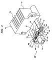
- Fig. 3 is a perspective view showing a state in which the light source module 100 is attached to the light source holding member 60.
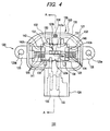
- Fig. 4 is a plan view of the light source module 100.
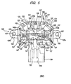
- Fig. 5 is a sectional view of the light source module 100 taken along the line A-A shown in Fig. 4 .
- the light source module 100 includes a power feeding attachment 120 and a circuit board 140.
- the power feeding attachment 120 supplies power to the light emitting diode 150 on the circuit board 140.
- the light source holding member 60 serves as a heat dissipating member that dissipates heat generated from the circuit board 140 of the light source module 100 and the light emitting diode 150 mounted on the circuit board 140.
- the light source holding member 60 includes a heat dissipating portion 61 having a plurality of rearwardly protruding heat dissipating fins 61 a, and a substantially flat-plate base part 62 protruding forward from the heat dissipating portion 61.
- the power feeding attachment 120 and the circuit board 140 are disposed on an upper surface of the base part 62.
- the base part 62 is provided as a single piece together with the heat dissipating portion 61 so as to protrude forward from the heat dissipating portion 61 of the light source holding member 60.
- the base part 62 is a substantially rectangular flat plate protruding from the front surface of the heat dissipating portion 61, and includes an attaching surface portion 64 provided on both left and right side portions and a front end portion of an upper surface thereof and a board mounting portion 63 provided by raising a portion of the upper surface other than the attaching surface portion 64 a step higher.
- the light source module 100 is attached to the front end side of the base part 62.
- the light source module 100 can be fixed to the base part 62 by placing the circuit board 140 on the board mounting portion 63 and then attaching the power feeding attachment 120 to the attaching surface portion 64 so as to press the circuit board 140 against the board mounting portion 63 from above.
- a plurality of positioning pins 63a for positioning the circuit board 140 on the board mounting portion 63 is provided so as to protrude upward when the circuit board 140 of the light source module 100 is placed on the board mounting portion 63.
- screw holes 64a are formed on both left and right sides of the attaching surface portion 64 and mounting screws 200 for fixing the power feeding attachment 120 of the light source module 100 are screwed to the screw holes 64a.
- ribs 64b are provided in front and back of the screw holes 64a of the attaching surface portion 64 to position attaching tab portions 125 of the power feeding attachment 120 on the attaching surface portion 64 when the power feeding attachment 120 is attached to the attaching surface portion 64.
- the circuit board 140 includes a non-conductive board part 141 and a conductive circuit 142 provided on the board part 141, and a plurality of light emitting diodes 150 (four in this example) are mounted on the central portion of the circuit board. These light emitting diodes 150 are examples of the semiconductor light emitting device in the present invention.
- the board part 141 is formed of, for example, an epoxy resin material.
- the conductive circuit 142 is formed of, for example, aluminum.
- the board part 141 may be a silicone board and, in this case, the conductive circuit 142 may be formed, for example, by copper plating on the silicone board.
- the conductive circuit 142 includes, for example, a light source connecting portion 142a and terminal portions 142b.
- the light source connecting portion 142a is electrically connected to the respective light emitting diodes 150 that are mounted on an upper surface thereof.
- the terminal portions 142b are circuit patterns and are continuous with the light source connecting portion 142a, and are provided in a pair at both left and right sides on the board part 141 with the light source connecting portion 142a interposed therebetween.
- the power feeding attachment 120 includes a resin molded portion (electrically-insulating portion) 121 formed of a non-conductive resin material and a conductive portion 131 formed of a conductive material such as metal (see Fig. 2 to Fig. 4 ).
- the conductive portion 131 is embedded in the resin molded portion 121 except a portion thereof.
- the resin material used for forming the resin molded portion 121 is a material having higher thermal conductivity, for example, thermal conductivity of 5.0 to 10.0 [W/m ⁇ K], than a resin material (thermal conductivity of 1.0 [W/m ⁇ K] or less) used in a conventional resin molded portion. More specifically, as the material forming the resin molded portion 121, for example, nylon resin is preferably used.
- the power feeding attachment 120 is formed by, for example, so-called insert molding in which the conductive portion 131 is placed at a given position inside the cavity of a molding die and molten resin filling the cavity is cured. In this way, the conductive portion 131 and the resin molded portion 121 are integrally molded.
- the resin molded portion 121 is an example of the electrically-insulating portion according to the present invention, and includes a frame portion 123, a connector case portion 124 protruding forward from the frame portion 123, and attaching tab portions 125 protruding respectively in left and right directions from the frame portion 123.
- An opening 126 for disposing the circuit board 140 therein is provided on an inner side of the frame portion 123.
- a positioning protrusion 123a protruding rearward is provided on the front inner surface of the opening 126 at the central portion in the left-right direction.
- a positioning protrusion 123b protruding forward is provided on the rear inner surface of the opening 126 at the central portion of a left-right direction.
- the circuit board 140 is positioned inside the opening 126 of the frame portion 123 by these positioning protrusions 123a, 123b when the power feeding attachment 120 and the circuit board 140 are attached to the base part 62.
- the connector case portion 124 has an outer form of a substantially rectangular tube-shape, and a concave space is formed inside an opening provided at a front side thereof.
- the connector terminal parts 133 of the conductive portion 131 to be described later protrude forward from a rear wall surface.
- Each of the attaching tab portions 125 is formed with, for example as shown in Fig. 2 and Fig. 3 , a screw insertion hole 125a penetrating in a vertical direction, and an upper surface thereof is lower than an upper surface of the frame portion 123.
- the power feeding attachment 120 can be attached to the base part 62 by placing the power feeding attachment 120 on the base part 62 and screwing the mounting screws 200 such that two screw insertion holes 125a provided in the attaching tab portions 125 corresponds to two screw holes 64a of the base part 62.
- the conductive portion 131 includes a substantially annular base body portion 132 entirely embedded in the resin molded portion 121, connector terminal parts 133 protruding forward from a front-side end portion (front end portion) of the base body portion 132, power feeding pieces 134 protruding inward from both left and right sides of the base body portion 132, a connecting portion 135 connecting rear-side end portions (rear end portions) of the base body portion 132, two pressing tab parts 137 protruding forward from a rear end portion of the base body part 132, and two pressing tab parts 138 protruding rearward from a front end portion of the base body part 132.
- the connecting portion is cut when the light source module 100 is attached to the base part 62 of the light source holding member 60 for use. In this way, the handling of the conductive portion 131 is improved.
- each connector terminal part 133 For each connector terminal part 133, a portion near the base body part 132 is embedded in the resin molded portion 121, and a portion (distal end portion) away from the base body part 132 is exposed from the resin molded portion 121 and protrudes forward from the rear wall surface of the interior of the connector case portion 124.
- the connector terminal parts 133 When a connector (not shown) is inserted into the connector case portion 124, the connector terminal parts 133 are electrically connected to terminals on the side of the connector.
- Each of the pressing tab parts 137, 138 is a plate-like member extending from the base body part 132, and contacts an outer peripheral portion of the circuit board 140 on which the conductive circuit 142 is not provided, thereby pressing the circuit board 140 toward the base part 62.
- the pressing tab parts 137, 138 may be formed of the same material as the conductive portion 131, however, it is preferable that the pressing tab parts 137, 138 are formed of a material having a high thermal conductivity.
- the light source module 100 is configured such that the circuit board 140 is pressed against the base part 62 of the light source holding member 60 by the resin molded portion 121 of the power feeding attachment 120 and the pressing tab parts 137, 138 when the power feeding attachment 120 is attached to the base part 62, so that the bottom surface of the circuit board 140 and the upper surface of the base part 62 are brought into firm contact with each other. Accordingly, heat generated from the light emitting diodes 150 and transmitted to the circuit board 140 can be released efficiently to the light source holding member 60.
- the resin molded portion 121 is formed of an electrically-insulating material having a higher thermal conductivity than the board part 141 of the circuit board 140, the heat that is generated from the light emitting diodes 150 and transmitted to the circuit board 140 can be released efficiently also through the portion of the resin molded portion 121 contacting the circuit board 140. Further, the heat generated by the light emitting diodes 150 can be released also through the power feeding pieces 134 contacting the terminal parts 142b of the circuit board 140.
- the pressing tab parts 137, 138 are formed of an electrically-insulating material, unlike the rest of the conductive portion 131, the pressing tab parts 137, 138 may be arranged to contact the conductive circuit 142 so as to more effectively transmit heat generated by the light emitting diodes 150 to the pressing tab parts 137, 138. While the pressing tab parts 137, 138 are provided two each in this example, the number and a position of the pressing tab parts are not limited to these configurations.
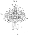
- the surface of the resin molded portion 121 may be provided with, for example as shown in Fig. 6 , a plurality of concave portions 127 in a region corresponding to the conductive portion 131 embedded therein.
- Fig. 6 is a plan view of a light source module 100A according to a modification of the first embodiment.
- a configuration of the light source module 100A of this example is different only partially from the foregoing light source module 100. Therefore, an exploded perspective view of the light source module 100A or a view showing a state in which the light source module 10A is attached to the light source holding member 60 is omitted, and the same configurations as in the light source modules 100 are denoted by the same reference numerals and a description thereof is omitted.
- the concave portions 127 are provided on the surface of the resin molded portion 121 in a region corresponding to the conductive portion 131, so that the thickness of the resin molded portion 121 near the conductive portion 131 is small, whereby the heat transmitted to the conductive portion 131 can be efficiently released to the air. Further, by providing the concave portion 127, the surface area of the resin molded portion 121 itself is increased as compared with a case in which there is no concave portion 127, whereby the efficiency of releasing the heat transmitted to the resin molded portion 121 to the air is improved.
- the concave portion 127 may be formed as a hole penetrating from the surface of the resin molded portion 121 to the conductive portion 131 such that a portion of the conductive portion 131 is exposed to the outside. By forming the concave portion 127 as a through hole, the heat transmitted to the conductive portion 131 can be further efficiently released to the air.
- a portion of the conductive portion 131 near the pressing tab parts 137, 138 may be exposed to the outside through the concave portion 127. In this way, the heat transmitted from the pressing tab parts 137, 138 pressing the outer peripheral portion of the circuit board 140 to the conductive portion 131 can be effectively released to the air.
- the concave portions 127 may be formed independently along the conductive portion 131 as shown in the drawing or a single concave portion 127 having a shape extending along the conductive portion 131 may be formed.
- Fig. 7 is a plan view of a light source module 101 according to a second embodiment of the present invention.
- a configuration of the light source module 101 of this example is different only partially from the light source modules 100. Therefore, an exploded perspective view of the light source module 101 or a view showing a state in which the light source module 101 is attached to the light source holding member 60 is omitted, and the same configurations as in the light source module 100 are denoted by the same reference numerals and a description thereof is omitted.
- the pressing tab part 137 is provided as a separate piece from the conductive portion 131, and extends to the rear of the resin molded portion 121 so as to detour an outer surface of the resin molded portion 121.
- the extended portion 139 of the pressing tab part 137 extending to the rear of the resin molded portion 121 contacts the surface of the board mounting portion 63 of the light source holding member 60 when the light source module 101 is attached to the light source holding member 60.
- the light source module 101 can more effectively release heat generated by the light emitting diodes 150 through the pressing tab part 137.
- the pressing tab part 137 is provided separately from the conductive portion 131, so that it is possible to use a material having a higher thermal conductivity than the conductive portion 131.
- the concave portions 127 may be formed in the surface of the resin molded portion 121 in a region of corresponding to the conductive portion 131, as shown in Fig. 8 . This makes it possible to efficiently release the heat transmitted to the conductive portion 131 to the air.
- Fig. 9 is a plan view of a light source module 102 according to a third embodiment of the present invention.
- a configuration of the light source module 102 of this example is different only partially from the light source modules 100, 101. Therefore, an exploded perspective view of the light source module 102 or a view showing a state in which the light source module 102 is attached to the light source holding member 60 is omitted, and the same configurations as in the light source modules 100, 101 are denoted by the same reference numerals and a description thereof is omitted.
- a portion of the base body part 132 of the conductive portion 131 extends outward (rearward) from the resin molded portion 121.
- This extended portion does not contact the light source holding member 60 when the light source module 102 is attached to the light source holding member 60.
- the extended portion may be brought into contact with the light source holding member 60 by forming the light source holding member 60 using a material having an electrically-insulating property.
- the light source module 102 can release heat generated by the light emitting diodes 150 into the air through a portion of the base body part 132 extending outward from the resin molded portion 121, and therefore, the heat dissipation efficiency is further improved.
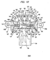
- the concave portions 127 may be formed in the surface of the resin molded portion 121 in a region of corresponding to the conductive portion 131, as shown in Fig. 10 . This makes it possible to effectively release the heat transmitted to the conductive portion 131 into the air.
- the light source module of the present invention because a portion (e.g., a back surface) of the circuit board is brought into firm contact with the mounting base of the light source holding member by the electrically-insulating portion of the power feeding attachment, heat generated by the semiconductor light emitting device can be effectively released to the light source holding member.
- the heat generated by the semiconductor light emitting device can be released also from the conductive portion contacting the terminal parts of the circuit board at the power feeding pieces and from the electrically-insulating portion that presses the circuit board against the mounting base.
- the light source module can be further downsized without impairing a heat release performance with regard to the heat generated by the semiconductor light emitting device.
- heat dissipating fin 62...mounting base, 63...board mounting portion, 63a...protrusion pin, 64...attaching surface portion, 64a...screw hole, 64b...positioning ridge, 70...support member, 100, 101, 102...light source module, 120...power feeding attachment, 121...resin molded portion (electrically-insulating portion), 123...frame portion, 123a, 123b...positioning protrusion, 123c...positioning portion, 124...connector case portion, 125...attaching piece portion, 125a...screw insertion hole, 126...opening, 127...concave portion, 131...conductive portion, 132...base body part, 133...connector terminal part, 134...power feeding piece, 135...connection part, 136...light source holding member, 137, 138...pressing tab part, 139...extended portion, 140...
- circuit board 141... board part, 142... conductive circuit, 142a... light source connecting portion, 142b... terminal portion, 150...light emitting diode (semiconductor light emitting device), 150a...light emitting surface, 200...mounting hole, ax...lamp optical axis
Landscapes
- Engineering & Computer Science (AREA)
- General Engineering & Computer Science (AREA)
- Physics & Mathematics (AREA)
- Microelectronics & Electronic Packaging (AREA)
- Optics & Photonics (AREA)
- Arrangement Of Elements, Cooling, Sealing, Or The Like Of Lighting Devices (AREA)
- Non-Portable Lighting Devices Or Systems Thereof (AREA)
- Led Device Packages (AREA)
Applications Claiming Priority (3)
| Application Number | Priority Date | Filing Date | Title |
|---|---|---|---|
| JP2011049102 | 2011-03-07 | ||
| JP2011074319 | 2011-03-30 | ||
| PCT/JP2012/053419 WO2012120979A1 (ja) | 2011-03-07 | 2012-02-14 | 光源モジュール |
Publications (1)
| Publication Number | Publication Date |
|---|---|
| EP2685154A1 true EP2685154A1 (de) | 2014-01-15 |
Family
ID=46797948
Family Applications (1)
| Application Number | Title | Priority Date | Filing Date |
|---|---|---|---|
| EP12754713.1A Withdrawn EP2685154A1 (de) | 2011-03-07 | 2012-02-14 | Lichtquellenmodul |
Country Status (5)
| Country | Link |
|---|---|
| US (1) | US9035346B2 (de) |
| EP (1) | EP2685154A1 (de) |
| JP (1) | JPWO2012120979A1 (de) |
| CN (1) | CN103415738B (de) |
| WO (1) | WO2012120979A1 (de) |
Families Citing this family (11)
| Publication number | Priority date | Publication date | Assignee | Title |
|---|---|---|---|---|
| JPWO2015041182A1 (ja) * | 2013-09-17 | 2017-03-02 | 株式会社小糸製作所 | アタッチメントおよび照明装置 |
| WO2016156463A1 (en) * | 2015-03-31 | 2016-10-06 | Koninklijke Philips N.V. | Led lighting module with heat sink and a method of replacing an led module |
| CN109073186B (zh) | 2016-04-18 | 2021-05-04 | 株式会社小糸制作所 | 供电配件及车辆用灯具 |
| US9945541B1 (en) | 2016-12-20 | 2018-04-17 | Keeper Technology Co., Ltd. | Light-emitting diode module holder |
| US10260696B2 (en) | 2016-12-22 | 2019-04-16 | Keeper Technology Co., Ltd. | Light-emitting diode module holder |
| US10066800B1 (en) | 2017-09-21 | 2018-09-04 | Keeper Technology Co., Ltd. | Light-emitting diode fixing apparatus |
| DE102019104792A1 (de) * | 2018-03-01 | 2019-09-05 | Nichia Corporation | Lichtemittierendes modul |
| JP2019220424A (ja) * | 2018-06-22 | 2019-12-26 | 東芝ライテック株式会社 | 車両用照明装置、および車両用灯具 |
| EP3620836B1 (de) * | 2018-09-05 | 2024-11-27 | ZKW Group GmbH | Dmd-modul |
| WO2021002336A1 (ja) * | 2019-07-04 | 2021-01-07 | 株式会社小糸製作所 | 光源ユニット、車両用灯具および光源ユニットの製造方法 |
| CN115199993B (zh) * | 2022-05-18 | 2024-04-12 | 深圳市力子光电科技有限公司 | 一种透镜式电器元件及发光设备 |
Family Cites Families (8)
| Publication number | Priority date | Publication date | Assignee | Title |
|---|---|---|---|---|
| ATE474443T1 (de) * | 2003-02-07 | 2010-07-15 | Panasonic Corp | Beleuchtungseinrichtung, einen sockel verwendend, um ein flaches led-modul auf einen kühlkörper zu montieren |
| JP4095463B2 (ja) * | 2003-02-13 | 2008-06-04 | 松下電器産業株式会社 | Led光源用ソケット |
| JP4535453B2 (ja) * | 2006-03-06 | 2010-09-01 | 株式会社小糸製作所 | 光源モジュール及び車輌用灯具 |
| JP4835605B2 (ja) * | 2008-02-19 | 2011-12-14 | 市光工業株式会社 | 車両用灯具 |
| JP5035995B2 (ja) * | 2008-03-21 | 2012-09-26 | 株式会社小糸製作所 | 光源モジュール及び車輌用灯具 |
| JP5479751B2 (ja) | 2009-02-16 | 2014-04-23 | 株式会社小糸製作所 | 光源モジュール及び車輌用灯具 |
| JP2011066133A (ja) * | 2009-09-16 | 2011-03-31 | Koito Mfg Co Ltd | 発光モジュール及び車輌用灯具 |
| US8342733B2 (en) * | 2009-12-14 | 2013-01-01 | Tyco Electronics Corporation | LED lighting assemblies |
-
2012
- 2012-02-14 US US14/003,158 patent/US9035346B2/en active Active
- 2012-02-14 JP JP2013503435A patent/JPWO2012120979A1/ja active Pending
- 2012-02-14 WO PCT/JP2012/053419 patent/WO2012120979A1/ja not_active Ceased
- 2012-02-14 CN CN201280012281.1A patent/CN103415738B/zh not_active Expired - Fee Related
- 2012-02-14 EP EP12754713.1A patent/EP2685154A1/de not_active Withdrawn
Also Published As
| Publication number | Publication date |
|---|---|
| CN103415738A (zh) | 2013-11-27 |
| WO2012120979A1 (ja) | 2012-09-13 |
| JPWO2012120979A1 (ja) | 2014-07-17 |
| US20130341670A1 (en) | 2013-12-26 |
| US9035346B2 (en) | 2015-05-19 |
| CN103415738B (zh) | 2016-04-27 |
Similar Documents
| Publication | Publication Date | Title |
|---|---|---|
| US9035346B2 (en) | Light source module | |
| US8950917B2 (en) | Vehicular lamp | |
| US8602619B2 (en) | Light source module and vehicle lamp | |
| JP5570331B2 (ja) | 車両用灯具 | |
| US8444308B2 (en) | Vehicular lamp | |
| EP2522898B1 (de) | Fahrzeugleuchte | |
| CN103486554B (zh) | 光源单元 | |
| JP4582087B2 (ja) | 発光ダイオードの固定構造 | |
| US10634329B2 (en) | Lamp unit and manufacturing method thereof | |
| JP5499005B2 (ja) | 半導体発光素子用ホルダ、半導体発光素子モジュール、及び、照明器具 | |
| JP6060677B2 (ja) | 車両用灯具 | |
| JP5479054B2 (ja) | 車両用灯具 | |
| JP2017191905A (ja) | 光源モジュール | |
| JP2016178009A (ja) | 車両用灯具 | |
| JP5749837B2 (ja) | 光源固定用アタッチメント | |
| JP6169455B2 (ja) | 光源モジュールを用いた車両用灯具 | |
| KR102148846B1 (ko) | 인쇄회로기판 조립체 및 이를 포함하는 발광장치 | |
| WO2023074674A1 (ja) | 車両用灯具 | |
| JP5702843B2 (ja) | 光源モジュール及び車輌用灯具 | |
| CN211232730U (zh) | 车辆用灯具 | |
| JP5406540B2 (ja) | 光源モジュール、車輌用灯具及び光源モジュールの製造方法 | |
| CN118829823A (zh) | 车辆用灯具用光源单元及车辆用灯具 | |
| JPWO2015041182A1 (ja) | アタッチメントおよび照明装置 | |
| JP2018206724A (ja) | 光源モジュール | |
| JP2013229184A (ja) | 照明装置 |
Legal Events
| Date | Code | Title | Description |
|---|---|---|---|
| PUAI | Public reference made under article 153(3) epc to a published international application that has entered the european phase |
Free format text: ORIGINAL CODE: 0009012 |
|
| 17P | Request for examination filed |
Effective date: 20130905 |
|
| AK | Designated contracting states |
Kind code of ref document: A1 Designated state(s): AL AT BE BG CH CY CZ DE DK EE ES FI FR GB GR HR HU IE IS IT LI LT LU LV MC MK MT NL NO PL PT RO RS SE SI SK SM TR |
|
| DAX | Request for extension of the european patent (deleted) | ||
| STAA | Information on the status of an ep patent application or granted ep patent |
Free format text: STATUS: THE APPLICATION HAS BEEN WITHDRAWN |
|
| RIC1 | Information provided on ipc code assigned before grant |
Ipc: F21S 8/10 20060101AFI20151209BHEP Ipc: F21Y 101/02 00000000ALI20151209BHEP |
|
| 18W | Application withdrawn |
Effective date: 20151229 |