EP2763177A1 - Herstellungsverfahren eines MOS-Transistors mit Luftabstandhaltern - Google Patents
Herstellungsverfahren eines MOS-Transistors mit Luftabstandhaltern Download PDFInfo
- Publication number
- EP2763177A1 EP2763177A1 EP14153839.7A EP14153839A EP2763177A1 EP 2763177 A1 EP2763177 A1 EP 2763177A1 EP 14153839 A EP14153839 A EP 14153839A EP 2763177 A1 EP2763177 A1 EP 2763177A1
- Authority
- EP
- European Patent Office
- Prior art keywords
- layer
- gate
- stack
- length
- spacers
- Prior art date
- Legal status (The legal status is an assumption and is not a legal conclusion. Google has not performed a legal analysis and makes no representation as to the accuracy of the status listed.)
- Withdrawn
Links
Images

Classifications
-
- H—ELECTRICITY
- H10—SEMICONDUCTOR DEVICES; ELECTRIC SOLID-STATE DEVICES NOT OTHERWISE PROVIDED FOR
- H10D—INORGANIC ELECTRIC SEMICONDUCTOR DEVICES
- H10D64/00—Electrodes of devices having potential barriers
- H10D64/60—Electrodes characterised by their materials
- H10D64/66—Electrodes having a conductor capacitively coupled to a semiconductor by an insulator, e.g. MIS electrodes
-
- H—ELECTRICITY
- H10—SEMICONDUCTOR DEVICES; ELECTRIC SOLID-STATE DEVICES NOT OTHERWISE PROVIDED FOR
- H10D—INORGANIC ELECTRIC SEMICONDUCTOR DEVICES
- H10D30/00—Field-effect transistors [FET]
- H10D30/01—Manufacture or treatment
- H10D30/021—Manufacture or treatment of FETs having insulated gates [IGFET]
- H10D30/027—Manufacture or treatment of FETs having insulated gates [IGFET] of lateral single-gate IGFETs
- H10D30/0275—Manufacture or treatment of FETs having insulated gates [IGFET] of lateral single-gate IGFETs forming single crystalline semiconductor source or drain regions resulting in recessed gates, e.g. forming raised source or drain regions
-
- H—ELECTRICITY
- H10—SEMICONDUCTOR DEVICES; ELECTRIC SOLID-STATE DEVICES NOT OTHERWISE PROVIDED FOR
- H10D—INORGANIC ELECTRIC SEMICONDUCTOR DEVICES
- H10D64/00—Electrodes of devices having potential barriers
- H10D64/01—Manufacture or treatment
- H10D64/013—Manufacture or treatment of electrodes having a conductor capacitively coupled to a semiconductor by an insulator
-
- H—ELECTRICITY
- H10—SEMICONDUCTOR DEVICES; ELECTRIC SOLID-STATE DEVICES NOT OTHERWISE PROVIDED FOR
- H10D—INORGANIC ELECTRIC SEMICONDUCTOR DEVICES
- H10D64/00—Electrodes of devices having potential barriers
- H10D64/01—Manufacture or treatment
- H10D64/013—Manufacture or treatment of electrodes having a conductor capacitively coupled to a semiconductor by an insulator
- H10D64/01302—Manufacture or treatment of electrodes having a conductor capacitively coupled to a semiconductor by an insulator the insulator being formed after the semiconductor body, the semiconductor being silicon
- H10D64/01304—Manufacture or treatment of electrodes having a conductor capacitively coupled to a semiconductor by an insulator the insulator being formed after the semiconductor body, the semiconductor being silicon characterised by the conductor
- H10D64/01324—Manufacture or treatment of electrodes having a conductor capacitively coupled to a semiconductor by an insulator the insulator being formed after the semiconductor body, the semiconductor being silicon characterised by the conductor characterised by the sectional shape, e.g. T or inverted-T
-
- H—ELECTRICITY
- H10—SEMICONDUCTOR DEVICES; ELECTRIC SOLID-STATE DEVICES NOT OTHERWISE PROVIDED FOR
- H10D—INORGANIC ELECTRIC SEMICONDUCTOR DEVICES
- H10D64/00—Electrodes of devices having potential barriers
- H10D64/01—Manufacture or treatment
- H10D64/015—Manufacture or treatment removing at least parts of gate spacers, e.g. disposable spacers
-
- H—ELECTRICITY
- H10—SEMICONDUCTOR DEVICES; ELECTRIC SOLID-STATE DEVICES NOT OTHERWISE PROVIDED FOR
- H10D—INORGANIC ELECTRIC SEMICONDUCTOR DEVICES
- H10D64/00—Electrodes of devices having potential barriers
- H10D64/01—Manufacture or treatment
- H10D64/017—Manufacture or treatment using dummy gates in processes wherein at least parts of the final gates are self-aligned to the dummy gates, i.e. replacement gate processes
-
- H—ELECTRICITY
- H10—SEMICONDUCTOR DEVICES; ELECTRIC SOLID-STATE DEVICES NOT OTHERWISE PROVIDED FOR
- H10D—INORGANIC ELECTRIC SEMICONDUCTOR DEVICES
- H10D64/00—Electrodes of devices having potential barriers
- H10D64/01—Manufacture or treatment
- H10D64/021—Manufacture or treatment using multiple gate spacer layers, e.g. bilayered sidewall spacers
-
- H—ELECTRICITY
- H10—SEMICONDUCTOR DEVICES; ELECTRIC SOLID-STATE DEVICES NOT OTHERWISE PROVIDED FOR
- H10D—INORGANIC ELECTRIC SEMICONDUCTOR DEVICES
- H10D64/00—Electrodes of devices having potential barriers
- H10D64/20—Electrodes characterised by their shapes, relative sizes or dispositions
- H10D64/27—Electrodes not carrying the current to be rectified, amplified, oscillated or switched, e.g. gates
- H10D64/311—Gate electrodes for field-effect devices
- H10D64/411—Gate electrodes for field-effect devices for FETs
- H10D64/511—Gate electrodes for field-effect devices for FETs for IGFETs
- H10D64/517—Gate electrodes for field-effect devices for FETs for IGFETs characterised by the conducting layers
- H10D64/518—Gate electrodes for field-effect devices for FETs for IGFETs characterised by the conducting layers characterised by their lengths or sectional shapes
-
- H—ELECTRICITY
- H10—SEMICONDUCTOR DEVICES; ELECTRIC SOLID-STATE DEVICES NOT OTHERWISE PROVIDED FOR
- H10D—INORGANIC ELECTRIC SEMICONDUCTOR DEVICES
- H10D64/00—Electrodes of devices having potential barriers
- H10D64/60—Electrodes characterised by their materials
- H10D64/66—Electrodes having a conductor capacitively coupled to a semiconductor by an insulator, e.g. MIS electrodes
- H10D64/661—Electrodes having a conductor capacitively coupled to a semiconductor by an insulator, e.g. MIS electrodes the conductor comprising a layer of silicon contacting the insulator, e.g. polysilicon having vertical doping variation
- H10D64/662—Electrodes having a conductor capacitively coupled to a semiconductor by an insulator, e.g. MIS electrodes the conductor comprising a layer of silicon contacting the insulator, e.g. polysilicon having vertical doping variation the conductor further comprising additional layers, e.g. multiple silicon layers having different crystal structures
-
- H—ELECTRICITY
- H10—SEMICONDUCTOR DEVICES; ELECTRIC SOLID-STATE DEVICES NOT OTHERWISE PROVIDED FOR
- H10D—INORGANIC ELECTRIC SEMICONDUCTOR DEVICES
- H10D64/00—Electrodes of devices having potential barriers
- H10D64/60—Electrodes characterised by their materials
- H10D64/66—Electrodes having a conductor capacitively coupled to a semiconductor by an insulator, e.g. MIS electrodes
- H10D64/675—Gate sidewall spacers
- H10D64/679—Gate sidewall spacers comprising air gaps
Definitions
- the present invention relates to MOS transistors and more particularly to MOS transistors with air spacers.
- MOS transistor In the realization of a MOS transistor, it is generally sought to reduce switching consumption and increase the switching speed. These parameters depend in particular on the gate-source, gate-drain, source-gate-contact and drain-gate-contact capacities.
- parasitic capacitances tend to become particularly important in the case of MOS transistors of very small dimensions, in which the gate lengths are less than one hundred nanometers and in particular less than 20 nm. Indeed, in this case the distances between the gate, on the one hand, and the source, the drain, the source contact and the drain contact, on the other hand, become extremely low.
- One solution to reduce these parasitic capacitances is to surround the sides of the grid on either side of the length thereof of air spacers (vacuum) and not conventionally spacers of a material solid dielectric. This is for example described in the article " Air Spacer MOSFET Technology for 20nm Node and Beyond "by Jemin Park and Chenming Hu 9th ICSICT - October 20-23, 2008 - IEEE 2008 .
- the figure 1 attached reproduces the Figure 3 (d) of this article. It shows a MOS transistor at an intermediate stage of manufacture.
- This transistor is formed on a substrate covered with a gate stack.
- S / D source and drain regions
- the upper face of the gate carries an oxide (Mask Oxide).
- the grid and oxide covering it are surrounded by air spacers (Air Spacer).
- SAC self-aligned contact regions
- ILD2 insulating layer
- the air spacers illustrated in figure 1 result from the etching elimination of dielectric spacers previously formed on either side of the grid.
- an embodiment of the present invention provides an MOS transistor comprising, over a gate insulator, a gate conductive stack having a height, a length and a width, said stack having a low portion adjacent to the gate. gate insulator and an upper part, wherein said stack has a first length in its lower part, and a second length less than the first length in its upper part.
- the second length is equal to 0.3 to 0.9 times the first length.
- the grid conductive stack is lined with air spacers extending in the direction of its width.
- the gate conductive stack is further lined with dielectric spacers, delimiting the air spacers.
- the lower part of the gate conductive stack comprises at least one layer of a first material, and the upper part comprises at least one second material.
- the lower part comprises a portion of a layer of a metal.
- the upper part comprises a portion of a layer of a doped semiconductor.
- the layer of a doped semiconductor is a polycrystalline silicon or silicon-germanium layer.
- the lower part of the gate conductive stack comprises a layer of a metal or a metal alloy and a doped polycrystalline silicon layer
- the upper part comprises a doped polycrystalline silicon-germanium layer.
- the lower portion of the gate conductive stack comprises a layer of a first metal or metal alloy
- the upper portion comprises a layer of a second metal or metal alloy.
- air spacers has the advantage over the use of solid dielectric spacers that the air (or vacuum) has a very low dielectric constant, close to 1, whereas the commonly used materials in the field of microelectronics for spacers, such as silicon oxide or silicon nitride have dielectric constants greater than 2.5 or even 4.
- these spacers are obtained by first making solid dielectric spacers and then etching off these spacers and by plugging the upper part of the cavity. thus formed.
- the general dimensions of the spacers are therefore imposed by the technology.
- the transistor that one seeks to manufacture is a transistor of minimum dimensions, that is to say that the gate length (the dimension considered in the direction from the source to the drain ) of the transistor corresponds to the smallest dimension that can be obtained in a given technology.
- the length of the gate at its contact with the gate insulator is imposed by the technology.
- the grid is made in the form of a stack of conductive materials, the height of the gate being chosen, in particular, to make it possible to ensure a contact upwards, substantially at the same level as the contacts towards the zones of source and drain.
- the figure 2 schematically represents a modification of the structure represented in figure 1 , incorporating the principles outlined above.
- a substrate 1 in which are formed source and drain regions 2 and 3 on either side of a conductive grid formed on a gate insulator 4.
- the gate comprises a lower part or lower part 6 of length L1 in at least one first conductive material surmounted by an upper part 7 in at least a second conductive material of length L2 less than L1.
- the upper grid portion or upper portion is surmounted by an insulator 9 of the same length L1 as the low grid portion 6.
- the grid structure comprising the conductive grid 6-7 and the upper insulation 9 is laterally surrounded by spacers 10. These spacers are, as in the case of figure 1 , Empty spacers or air spacers 10. On either side of the air spacers are conductive regions 11 and 12, respectively source contact and drain contact.
- the entire structure is coated with an insulating layer 13.
- the structure described above derives directly from the structure described in the article " Air Spacer MOSFET Technology for 20nm Node and Beyond "by Jemin Park and Chenming Hu 9th ICSICT - October 20-23, 2008 - IEEE 2008 .
- This structure is susceptible of many variants.
- the second conductive material of the high gate portion 7 may be a doped semiconductor material.
- This high grid portion 7 may be surmounted by a conductive material rather than an insulator 9.
- the zones designated by the references 11 and 12 may be insulating regions.
- the figure 3 represents another embodiment of a MOS transistor with low parasitic air spacers.
- the structure comprises source and drain regions 2 and 3 and a gate isolation layer 4.
- the source and drain regions 2 and 3 may be formed in a portion of the upper surface of a substrate solid semiconductor or in a thin monocrystalline silicon layer formed on an insulator, itself generally formed on a semiconductor substrate not shown to form a so-called silicon on insulator structure commonly designated by the acronym SOI.
- SOI silicon on insulator structure commonly designated by the acronym SOI.
- the reference 21 designates either a semiconductor substrate, or an insulating layer.
- the lower portion of the gate conductive stack comprises two conductive regions 23 and 24, the lower region 23 preferably being a metal or metal alloy, the optional upper region preferably being a doped semiconductor material.
- the upper part 27 of the gate conductive stack is made of a selectively etchable conductive material with respect to the conducting materials 23 and 24.
- This upper part 27 has a length L2 less than the length L1 of the lower part 23-24.
- the intermediate layer 24 is provided to improve the contact between the upper part 27 and the lower part 23 and ensure that the lower part of the gate is well equipotential.
- the structure is surmounted by a region 29, insulating or conductive, which, in the example shown, is of the same length L1 as the lower part 23-24 of this gate stack.
- the gate structure is surrounded by an air spacer 10, itself surrounded by a second spacer 30 of a solid dielectric material.
- Source and drain regions 31, 32 are also represented, above source and drain regions, semiconductor source and drain regions 31, 32, commonly provided in the case where the layer 2 is a very thin layer of silicon on insulator. Outside the spacers 30 are the source and drain contact regions 11 and 12 and the assembly is surmounted by an insulating layer 13.
- the structure can be obtained by a process substantially identical to that described in connection with the figure 2 .
- a first spacer which will be replaced by the air spacer
- epitaxial regions 31 and 32 of thickening of the source and drain regions are formed.
- the second spacer 30 is then formed and then the first intermediate spacer is etched off to form the air spacer 10.
- the two spacers can also be removed to form a larger air spacer.
- the second spacer 30 may be silicon oxide.
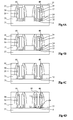
- FIGS 4A to 4D represent successive steps of manufacturing another embodiment of MOS transistor with low gate-source and gate-drain air spacers. These figures are sectional views showing two transistors side by side, the drain of one being connected to the source of the other.
- the Figure 4B represents the structure of the Figure 4A after removal by chemical mechanical etching (CMP) of the upper insulating layer 13.
- CMP chemical mechanical etching
- a new gate metal 50 is deposited by a conformal physical or chemical method, this metal may be selected from the group consisting of W, Ti and TiN. Deposition of the metal 50 may be preceded by a deposition step of a gate isolation layer. Note that in this embodiment, an air bubble 60 may appear at the location shown.
- MOS transistors have been described. Various variations and modifications will be apparent to those skilled in the art.
- the present description has been made by mentioning MOS transistors.
- MOS transistor must be interpreted in the broad sense and covers in particular the cases where the structure concerned constitutes a switching transistor or a memory point, and a single or double gate structure.
- MOS transistors have been described and shown here in which the source and drain contacts are self-aligned on the gate spacers, the present application is also directed to the case of non-self-aligned contacts.
Landscapes
- Insulated Gate Type Field-Effect Transistor (AREA)
- Chemical & Material Sciences (AREA)
- Crystallography & Structural Chemistry (AREA)
- Electrodes Of Semiconductors (AREA)
Applications Claiming Priority (1)
| Application Number | Priority Date | Filing Date | Title |
|---|---|---|---|
| FR1350941A FR3001831B1 (fr) | 2013-02-04 | 2013-02-04 | Transistor mos a espaceurs d'air |
Publications (1)
| Publication Number | Publication Date |
|---|---|
| EP2763177A1 true EP2763177A1 (de) | 2014-08-06 |
Family
ID=48140038
Family Applications (1)
| Application Number | Title | Priority Date | Filing Date |
|---|---|---|---|
| EP14153839.7A Withdrawn EP2763177A1 (de) | 2013-02-04 | 2014-02-04 | Herstellungsverfahren eines MOS-Transistors mit Luftabstandhaltern |
Country Status (3)
| Country | Link |
|---|---|
| US (1) | US9117805B2 (de) |
| EP (1) | EP2763177A1 (de) |
| FR (1) | FR3001831B1 (de) |
Families Citing this family (12)
| Publication number | Priority date | Publication date | Assignee | Title |
|---|---|---|---|---|
| US8866297B2 (en) * | 2012-11-30 | 2014-10-21 | Taiwan Semiconductor Manufacturing Company, Ltd. | Air-gap formation in interconnect structures |
| US9252233B2 (en) * | 2014-03-12 | 2016-02-02 | Taiwan Semiconductor Manufacturing Co., Ltd. | Air-gap offset spacer in FinFET structure |
| EP3696862A1 (de) * | 2015-07-17 | 2020-08-19 | INTEL Corporation | Transistor mit luftspalt-spacer |
| US9368572B1 (en) | 2015-11-21 | 2016-06-14 | International Business Machines Corporation | Vertical transistor with air-gap spacer |
| US9660050B1 (en) * | 2015-11-25 | 2017-05-23 | International Business Machines Corporation | Replacement low-k spacer |
| US10431661B2 (en) * | 2015-12-23 | 2019-10-01 | Intel Corporation | Transistor with inner-gate spacer |
| US10211092B1 (en) | 2018-01-28 | 2019-02-19 | International Business Machines Corporation | Transistor with robust air spacer |
| US10580692B1 (en) | 2018-09-12 | 2020-03-03 | International Business Machines Corporation | Integration of air spacer with self-aligned contact in transistor |
| US11532561B2 (en) | 2019-09-30 | 2022-12-20 | Taiwan Semiconductor Manufacturing Co., Ltd. | Different via configurations for different via interface requirements |
| KR102840198B1 (ko) | 2019-09-30 | 2025-08-01 | 삼성전자주식회사 | 반도체 장치 |
| US20230290855A1 (en) * | 2022-03-11 | 2023-09-14 | HeFeChip Corporation Limited | Transistor structure having an air spacer and method for making the same |
| US12176405B1 (en) * | 2024-05-15 | 2024-12-24 | Globalfoundries Singapore Pte. Ltd. | Field-effect transistors with airgap spacers |
Citations (5)
| Publication number | Priority date | Publication date | Assignee | Title |
|---|---|---|---|---|
| US5583067A (en) * | 1993-01-22 | 1996-12-10 | Intel Corporation | Inverse T-gate semiconductor device with self-aligned punchthrough stops and method of fabrication |
| US5869374A (en) * | 1998-04-22 | 1999-02-09 | Texas Instruments-Acer Incorporated | Method to form mosfet with an inverse T-shaped air-gap gate structure |
| US6001695A (en) | 1998-03-02 | 1999-12-14 | Texas Instruments - Acer Incorporated | Method to form ultra-short channel MOSFET with a gate-side airgap structure |
| US20020163036A1 (en) * | 2001-05-01 | 2002-11-07 | Mitsubishi Denki Kabushiki Kaisha | Semiconductor Device |
| US20080254579A1 (en) * | 2007-04-13 | 2008-10-16 | Taiwan Semiconductor Manufacturing Co., Ltd. | Semiconductor device and fabrication thereof |
Family Cites Families (20)
| Publication number | Priority date | Publication date | Assignee | Title |
|---|---|---|---|---|
| US6448140B1 (en) * | 1999-02-08 | 2002-09-10 | Taiwan Semiconductor Manufacturing Company | Laterally recessed tungsten silicide gate structure used with a self-aligned contact structure including a straight walled sidewall spacer while filling recess |
| KR100308619B1 (ko) * | 1999-08-24 | 2001-11-01 | 윤종용 | 반도체 장치용 자기 정렬 콘택 패드 형성 방법 |
| US6420218B1 (en) * | 2000-04-24 | 2002-07-16 | Advanced Micro Devices, Inc. | Ultra-thin-body SOI MOS transistors having recessed source and drain regions |
| KR100354438B1 (ko) * | 2000-12-12 | 2002-09-28 | 삼성전자 주식회사 | 모스 트랜지스터의 실리콘 게르마늄 게이트 폴리 형성방법 및 이를 이용한 씨모스 트랜지스터 형성 방법 |
| US6596599B1 (en) * | 2001-07-16 | 2003-07-22 | Taiwan Semiconductor Manufacturing Company | Gate stack for high performance sub-micron CMOS devices |
| US7078284B2 (en) * | 2002-06-20 | 2006-07-18 | Micron Technology, Inc. | Method for forming a notched gate |
| US7381610B2 (en) * | 2005-11-04 | 2008-06-03 | International Business Machines Corporation | Semiconductor transistors with contact holes close to gates |
| US7691712B2 (en) * | 2006-06-21 | 2010-04-06 | International Business Machines Corporation | Semiconductor device structures incorporating voids and methods of fabricating such structures |
| US7736981B2 (en) * | 2008-05-01 | 2010-06-15 | International Business Machines Corporation | Metal high dielectric constant transistor with reverse-T gate |
| US20090275182A1 (en) * | 2008-05-01 | 2009-11-05 | International Business Machines Corporation | Method for fabricating a metal high dielectric constant transistor with reverse-t gate |
| US8217470B2 (en) * | 2009-02-12 | 2012-07-10 | International Business Machines Corporation | Field effect device including recessed and aligned germanium containing channel |
| US8202776B2 (en) * | 2009-04-22 | 2012-06-19 | Taiwan Semiconductor Manufacturing Company, Ltd. | Method for protecting a gate structure during contact formation |
| US8536654B2 (en) * | 2010-01-13 | 2013-09-17 | Texas Instruments Incorporated | Structure and method for dual work function metal gate CMOS with selective capping |
| US8564066B2 (en) * | 2010-06-18 | 2013-10-22 | International Business Machines Corporation | Interface-free metal gate stack |
| US20120199886A1 (en) * | 2011-02-03 | 2012-08-09 | International Business Machines Corporation | Sealed air gap for semiconductor chip |
| KR101887414B1 (ko) * | 2012-03-20 | 2018-08-10 | 삼성전자 주식회사 | 반도체 장치 및 그 제조 방법 |
| US20130299920A1 (en) * | 2012-05-08 | 2013-11-14 | Haizhou Yin | Semiconductor device and method for manufacturing the same |
| KR101967614B1 (ko) * | 2012-07-20 | 2019-04-10 | 삼성전자 주식회사 | 반도체 소자 제조 방법 |
| US9190486B2 (en) * | 2012-11-20 | 2015-11-17 | Globalfoundries Inc. | Integrated circuits and methods for fabricating integrated circuits with reduced parasitic capacitance |
| KR20140108982A (ko) * | 2013-03-04 | 2014-09-15 | 삼성전자주식회사 | 메모리 장치 및 그 제조 방법 |
-
2013
- 2013-02-04 FR FR1350941A patent/FR3001831B1/fr active Active
-
2014
- 2014-01-31 US US14/169,913 patent/US9117805B2/en active Active
- 2014-02-04 EP EP14153839.7A patent/EP2763177A1/de not_active Withdrawn
Patent Citations (5)
| Publication number | Priority date | Publication date | Assignee | Title |
|---|---|---|---|---|
| US5583067A (en) * | 1993-01-22 | 1996-12-10 | Intel Corporation | Inverse T-gate semiconductor device with self-aligned punchthrough stops and method of fabrication |
| US6001695A (en) | 1998-03-02 | 1999-12-14 | Texas Instruments - Acer Incorporated | Method to form ultra-short channel MOSFET with a gate-side airgap structure |
| US5869374A (en) * | 1998-04-22 | 1999-02-09 | Texas Instruments-Acer Incorporated | Method to form mosfet with an inverse T-shaped air-gap gate structure |
| US20020163036A1 (en) * | 2001-05-01 | 2002-11-07 | Mitsubishi Denki Kabushiki Kaisha | Semiconductor Device |
| US20080254579A1 (en) * | 2007-04-13 | 2008-10-16 | Taiwan Semiconductor Manufacturing Co., Ltd. | Semiconductor device and fabrication thereof |
Non-Patent Citations (1)
| Title |
|---|
| JEMIN PARK; CHENMING HU: "Air Spacer MOSFET Technology for 20nm Node and Beyond", 9TH ICSICT - 20-23 OCTOBRE 2008 - IEEE, 2008 |
Also Published As
| Publication number | Publication date |
|---|---|
| US20140217520A1 (en) | 2014-08-07 |
| FR3001831A1 (fr) | 2014-08-08 |
| FR3001831B1 (fr) | 2016-11-04 |
| US9117805B2 (en) | 2015-08-25 |
Similar Documents
| Publication | Publication Date | Title |
|---|---|---|
| EP2763177A1 (de) | Herstellungsverfahren eines MOS-Transistors mit Luftabstandhaltern | |
| FR3011386A1 (fr) | Transistor mos a espaceurs d'air | |
| FR2838238A1 (fr) | Dispositif semiconducteur a grille enveloppante encapsule dans un milieu isolant | |
| FR2795555A1 (fr) | Procede de fabrication d'un dispositif semi-conducteur comprenant un empilement forme alternativement de couches de silicium et de couches de materiau dielectrique | |
| FR2823009A1 (fr) | Procede de fabrication d'un transistor vertical a grille isolee a faible recouvrement de la grille sur la source et sur le drain, et circuit integre comportant un tel transistor | |
| FR2853454A1 (fr) | Transistor mos haute densite | |
| FR2823010A1 (fr) | Procede de fabrication d'un transistor vertical a grille isolee a quadruple canal de conduction, et circuit integre comportant un tel transistor | |
| EP1869712B1 (de) | Struktur und verfahren zur realisierung einer mit einer anzahl von quantenleitungen ausgestatteten mikroelektronischen einrichtung mit der fähigkeit zur bildung eines oder mehrerer transistorkanäle | |
| FR2990295A1 (fr) | Procede de formation de contacts de grille, de source et de drain sur un transistor mos | |
| WO2001001477A1 (fr) | Procede de gravure laterale par trous pour fabriquer des dispositifs semi-conducteurs | |
| WO2007110507A2 (fr) | Procede de realisation d'un transistor a effet de champ a grilles auto-alignees | |
| EP3404723B1 (de) | Herstellung eines mos-transistors auf der basis eines 2d-halbleitermaterials | |
| EP1589572B1 (de) | Verfahren zur Herstellung einer integrierten Schaltung mit einem Isolationsgraben | |
| FR2928029A1 (fr) | Procede de fabrication d'un dispositif semi-conducteur a grille enterree et circuit integre correspondant. | |
| FR2799307A1 (fr) | Dispositif semi-conducteur combinant les avantages des architectures massives et soi, procede de fabrication | |
| FR3040538A1 (fr) | Transistor mos et son procede de fabrication | |
| FR3007198A1 (fr) | Composant, par exemple transistor nmos, a region active a contraintes en compression relachees, et procede de fabrication | |
| EP3188234B1 (de) | Integrierter schaltkreis und sein herstellungsverfahren | |
| FR3049110A1 (fr) | Procede de fabrication d'un transistor a effet de champ a capacite parasite reduite | |
| FR2976401A1 (fr) | Composant electronique comportant un ensemble de transistors mosfet et procede de fabrication | |
| EP2259304B1 (de) | Herstellungsverfahren einer Ebene eines dreidimensionalen Bauelements mithilfe einer dreidimensionalen sequenziellen Integration | |
| FR2871294A1 (fr) | Procede de realisation d'un transistor dmos de taille reduite, et transistor dmos en resultant | |
| WO2007017613A1 (fr) | Procede de fabrication d'un transistor a nanodoigts semiconducteurs paralleles | |
| FR3055469A1 (fr) | Transistor a effet de champ a grille entourante | |
| EP1746643B1 (de) | Herstellungsverfahren eines MOS-Transistors. |
Legal Events
| Date | Code | Title | Description |
|---|---|---|---|
| PUAI | Public reference made under article 153(3) epc to a published international application that has entered the european phase |
Free format text: ORIGINAL CODE: 0009012 |
|
| 17P | Request for examination filed |
Effective date: 20140204 |
|
| AK | Designated contracting states |
Kind code of ref document: A1 Designated state(s): AL AT BE BG CH CY CZ DE DK EE ES FI FR GB GR HR HU IE IS IT LI LT LU LV MC MK MT NL NO PL PT RO RS SE SI SK SM TR |
|
| AX | Request for extension of the european patent |
Extension state: BA ME |
|
| R17P | Request for examination filed (corrected) |
Effective date: 20141020 |
|
| RBV | Designated contracting states (corrected) |
Designated state(s): AL AT BE BG CH CY CZ DE DK EE ES FI FR GB GR HR HU IE IS IT LI LT LU LV MC MK MT NL NO PL PT RO RS SE SI SK SM TR |
|
| GRAP | Despatch of communication of intention to grant a patent |
Free format text: ORIGINAL CODE: EPIDOSNIGR1 |
|
| INTG | Intention to grant announced |
Effective date: 20150313 |
|
| STAA | Information on the status of an ep patent application or granted ep patent |
Free format text: STATUS: THE APPLICATION IS DEEMED TO BE WITHDRAWN |
|
| 18D | Application deemed to be withdrawn |
Effective date: 20150724 |