EP2793268B1 - Procédé de fabrication d'un dispositif à semi-conducteurs - Google Patents
Procédé de fabrication d'un dispositif à semi-conducteurs Download PDFInfo
- Publication number
- EP2793268B1 EP2793268B1 EP13769834.6A EP13769834A EP2793268B1 EP 2793268 B1 EP2793268 B1 EP 2793268B1 EP 13769834 A EP13769834 A EP 13769834A EP 2793268 B1 EP2793268 B1 EP 2793268B1
- Authority
- EP
- European Patent Office
- Prior art keywords
- layer
- semiconductor substrate
- semiconductor device
- rear surface
- semiconductor
- Prior art date
- Legal status (The legal status is an assumption and is not a legal conclusion. Google has not performed a legal analysis and makes no representation as to the accuracy of the status listed.)
- Active
Links
Images











Classifications
-
- H—ELECTRICITY
- H10—SEMICONDUCTOR DEVICES; ELECTRIC SOLID-STATE DEVICES NOT OTHERWISE PROVIDED FOR
- H10D—INORGANIC ELECTRIC SEMICONDUCTOR DEVICES
- H10D12/00—Bipolar devices controlled by the field effect, e.g. insulated-gate bipolar transistors [IGBT]
- H10D12/01—Manufacture or treatment
- H10D12/031—Manufacture or treatment of IGBTs
- H10D12/032—Manufacture or treatment of IGBTs of vertical IGBTs
-
- H—ELECTRICITY
- H10—SEMICONDUCTOR DEVICES; ELECTRIC SOLID-STATE DEVICES NOT OTHERWISE PROVIDED FOR
- H10D—INORGANIC ELECTRIC SEMICONDUCTOR DEVICES
- H10D12/00—Bipolar devices controlled by the field effect, e.g. insulated-gate bipolar transistors [IGBT]
- H10D12/01—Manufacture or treatment
- H10D12/031—Manufacture or treatment of IGBTs
- H10D12/032—Manufacture or treatment of IGBTs of vertical IGBTs
- H10D12/038—Manufacture or treatment of IGBTs of vertical IGBTs having a recessed gate, e.g. trench-gate IGBTs
-
- H—ELECTRICITY
- H10—SEMICONDUCTOR DEVICES; ELECTRIC SOLID-STATE DEVICES NOT OTHERWISE PROVIDED FOR
- H10D—INORGANIC ELECTRIC SEMICONDUCTOR DEVICES
- H10D12/00—Bipolar devices controlled by the field effect, e.g. insulated-gate bipolar transistors [IGBT]
- H10D12/411—Insulated-gate bipolar transistors [IGBT]
-
- H—ELECTRICITY
- H10—SEMICONDUCTOR DEVICES; ELECTRIC SOLID-STATE DEVICES NOT OTHERWISE PROVIDED FOR
- H10D—INORGANIC ELECTRIC SEMICONDUCTOR DEVICES
- H10D12/00—Bipolar devices controlled by the field effect, e.g. insulated-gate bipolar transistors [IGBT]
- H10D12/411—Insulated-gate bipolar transistors [IGBT]
- H10D12/441—Vertical IGBTs
- H10D12/461—Vertical IGBTs having non-planar surfaces, e.g. having trenches, recesses or pillars in the surfaces of the emitter, base or collector regions
- H10D12/481—Vertical IGBTs having non-planar surfaces, e.g. having trenches, recesses or pillars in the surfaces of the emitter, base or collector regions having gate structures on slanted surfaces, on vertical surfaces, or in grooves, e.g. trench gate IGBTs
-
- H—ELECTRICITY
- H10—SEMICONDUCTOR DEVICES; ELECTRIC SOLID-STATE DEVICES NOT OTHERWISE PROVIDED FOR
- H10D—INORGANIC ELECTRIC SEMICONDUCTOR DEVICES
- H10D62/00—Semiconductor bodies, or regions thereof, of devices having potential barriers
- H10D62/10—Shapes, relative sizes or dispositions of the regions of the semiconductor bodies; Shapes of the semiconductor bodies
- H10D62/129—Cathode regions of diodes
-
- H—ELECTRICITY
- H10—SEMICONDUCTOR DEVICES; ELECTRIC SOLID-STATE DEVICES NOT OTHERWISE PROVIDED FOR
- H10D—INORGANIC ELECTRIC SEMICONDUCTOR DEVICES
- H10D62/00—Semiconductor bodies, or regions thereof, of devices having potential barriers
- H10D62/10—Shapes, relative sizes or dispositions of the regions of the semiconductor bodies; Shapes of the semiconductor bodies
- H10D62/13—Semiconductor regions connected to electrodes carrying current to be rectified, amplified or switched, e.g. source or drain regions
- H10D62/141—Anode or cathode regions of thyristors; Collector or emitter regions of gated bipolar-mode devices, e.g. of IGBTs
- H10D62/142—Anode regions of thyristors or collector regions of gated bipolar-mode devices
-
- H—ELECTRICITY
- H10—SEMICONDUCTOR DEVICES; ELECTRIC SOLID-STATE DEVICES NOT OTHERWISE PROVIDED FOR
- H10D—INORGANIC ELECTRIC SEMICONDUCTOR DEVICES
- H10D62/00—Semiconductor bodies, or regions thereof, of devices having potential barriers
- H10D62/50—Physical imperfections
- H10D62/53—Physical imperfections the imperfections being within the semiconductor body
-
- H—ELECTRICITY
- H10—SEMICONDUCTOR DEVICES; ELECTRIC SOLID-STATE DEVICES NOT OTHERWISE PROVIDED FOR
- H10D—INORGANIC ELECTRIC SEMICONDUCTOR DEVICES
- H10D62/00—Semiconductor bodies, or regions thereof, of devices having potential barriers
- H10D62/60—Impurity distributions or concentrations
-
- H—ELECTRICITY
- H10—SEMICONDUCTOR DEVICES; ELECTRIC SOLID-STATE DEVICES NOT OTHERWISE PROVIDED FOR
- H10D—INORGANIC ELECTRIC SEMICONDUCTOR DEVICES
- H10D62/00—Semiconductor bodies, or regions thereof, of devices having potential barriers
- H10D62/80—Semiconductor bodies, or regions thereof, of devices having potential barriers characterised by the materials
- H10D62/81—Semiconductor bodies, or regions thereof, of devices having potential barriers characterised by the materials of structures exhibiting quantum-confinement effects, e.g. single quantum wells; of structures having periodic or quasi-periodic potential variation
- H10D62/815—Semiconductor bodies, or regions thereof, of devices having potential barriers characterised by the materials of structures exhibiting quantum-confinement effects, e.g. single quantum wells; of structures having periodic or quasi-periodic potential variation of structures having periodic or quasi-periodic potential variation, e.g. superlattices or multiple quantum wells [MQW]
- H10D62/8161—Semiconductor bodies, or regions thereof, of devices having potential barriers characterised by the materials of structures exhibiting quantum-confinement effects, e.g. single quantum wells; of structures having periodic or quasi-periodic potential variation of structures having periodic or quasi-periodic potential variation, e.g. superlattices or multiple quantum wells [MQW] potential variation due to variations in composition or crystallinity, e.g. heterojunction superlattices
- H10D62/8162—Semiconductor bodies, or regions thereof, of devices having potential barriers characterised by the materials of structures exhibiting quantum-confinement effects, e.g. single quantum wells; of structures having periodic or quasi-periodic potential variation of structures having periodic or quasi-periodic potential variation, e.g. superlattices or multiple quantum wells [MQW] potential variation due to variations in composition or crystallinity, e.g. heterojunction superlattices having quantum effects only in the vertical direction, i.e. layered structures having quantum effects solely resulting from vertical potential variation
- H10D62/8164—Semiconductor bodies, or regions thereof, of devices having potential barriers characterised by the materials of structures exhibiting quantum-confinement effects, e.g. single quantum wells; of structures having periodic or quasi-periodic potential variation of structures having periodic or quasi-periodic potential variation, e.g. superlattices or multiple quantum wells [MQW] potential variation due to variations in composition or crystallinity, e.g. heterojunction superlattices having quantum effects only in the vertical direction, i.e. layered structures having quantum effects solely resulting from vertical potential variation comprising only semiconductor materials
-
- H—ELECTRICITY
- H10—SEMICONDUCTOR DEVICES; ELECTRIC SOLID-STATE DEVICES NOT OTHERWISE PROVIDED FOR
- H10D—INORGANIC ELECTRIC SEMICONDUCTOR DEVICES
- H10D8/00—Diodes
- H10D8/01—Manufacture or treatment
- H10D8/043—Manufacture or treatment of planar diodes
-
- H—ELECTRICITY
- H10—SEMICONDUCTOR DEVICES; ELECTRIC SOLID-STATE DEVICES NOT OTHERWISE PROVIDED FOR
- H10D—INORGANIC ELECTRIC SEMICONDUCTOR DEVICES
- H10D8/00—Diodes
- H10D8/411—PN diodes having planar bodies
-
- H—ELECTRICITY
- H10—SEMICONDUCTOR DEVICES; ELECTRIC SOLID-STATE DEVICES NOT OTHERWISE PROVIDED FOR
- H10P—GENERIC PROCESSES OR APPARATUS FOR THE MANUFACTURE OR TREATMENT OF DEVICES COVERED BY CLASS H10
- H10P30/00—Ion implantation into wafers, substrates or parts of devices
- H10P30/20—Ion implantation into wafers, substrates or parts of devices into semiconductor materials, e.g. for doping
- H10P30/202—Ion implantation into wafers, substrates or parts of devices into semiconductor materials, e.g. for doping characterised by the semiconductor materials
- H10P30/204—Ion implantation into wafers, substrates or parts of devices into semiconductor materials, e.g. for doping characterised by the semiconductor materials into Group IV semiconductors
-
- H—ELECTRICITY
- H10—SEMICONDUCTOR DEVICES; ELECTRIC SOLID-STATE DEVICES NOT OTHERWISE PROVIDED FOR
- H10P—GENERIC PROCESSES OR APPARATUS FOR THE MANUFACTURE OR TREATMENT OF DEVICES COVERED BY CLASS H10
- H10P30/00—Ion implantation into wafers, substrates or parts of devices
- H10P30/20—Ion implantation into wafers, substrates or parts of devices into semiconductor materials, e.g. for doping
- H10P30/21—Ion implantation into wafers, substrates or parts of devices into semiconductor materials, e.g. for doping of electrically active species
-
- H—ELECTRICITY
- H10—SEMICONDUCTOR DEVICES; ELECTRIC SOLID-STATE DEVICES NOT OTHERWISE PROVIDED FOR
- H10P—GENERIC PROCESSES OR APPARATUS FOR THE MANUFACTURE OR TREATMENT OF DEVICES COVERED BY CLASS H10
- H10P30/00—Ion implantation into wafers, substrates or parts of devices
- H10P30/20—Ion implantation into wafers, substrates or parts of devices into semiconductor materials, e.g. for doping
- H10P30/28—Ion implantation into wafers, substrates or parts of devices into semiconductor materials, e.g. for doping characterised by an annealing step, e.g. for activation of dopants
-
- H—ELECTRICITY
- H10—SEMICONDUCTOR DEVICES; ELECTRIC SOLID-STATE DEVICES NOT OTHERWISE PROVIDED FOR
- H10P—GENERIC PROCESSES OR APPARATUS FOR THE MANUFACTURE OR TREATMENT OF DEVICES COVERED BY CLASS H10
- H10P34/00—Irradiation with electromagnetic or particle radiation of wafers, substrates or parts of devices
-
- H—ELECTRICITY
- H10—SEMICONDUCTOR DEVICES; ELECTRIC SOLID-STATE DEVICES NOT OTHERWISE PROVIDED FOR
- H10P—GENERIC PROCESSES OR APPARATUS FOR THE MANUFACTURE OR TREATMENT OF DEVICES COVERED BY CLASS H10
- H10P95/00—Generic processes or apparatus for manufacture or treatments not covered by the other groups of this subclass
- H10P95/94—Hydrogenation or deuterisation, e.g. using atomic hydrogen from a plasma
Definitions
- an insulated gate bipolar transistor (IGBT) or a diode with a breakdown voltage of 400 V, 600 V, 1200 V, 1700 V, 3300 V, or more has been known as a power semiconductor device.
- the power semiconductor device is used in a power conversion device, such as a converter or an inverter.
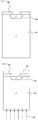
- FIGS. 26 to 31 are cross-sectional views illustrating the semiconductor device according to the related art which is being manufactured.
- Fig. 32 is a cross-sectional view illustrating the semiconductor device after a process which follows the process illustrated in Fig. 31 .
- a trench-gate-type MOS gate (metal-oxide-semiconductor insulated gate) structure including a p base region 102, an n + emitter region 103, a trench 104, a gate oxide film 105, and a gate electrode 106 are formed on the front surface of the semiconductor substrate.
- Reference numeral 108 is an interlayer insulating film.
- an emitter electrode 107 is formed so as to come into contact with the p base region 102 and the n + emitter region 103.
- the rear surface of the semiconductor substrate is removed by, for example, grinding to reduce the thickness of the semiconductor substrate.
- a proton (H + ) 121 is radiated to the ground rear surface of the semiconductor substrate.
- an "x" mark in the vicinity of the rear surface of the semiconductor substrate indicates the radiated proton (which holds for Figs. 7 , 11 , 18 , 22 , 48 , 50 , and 52 ).
- the proton 121 radiated to the semiconductor substrate is activated by annealing to form an n field stop (FS) layer 110 in the n - drift layer 101 in the vicinity of the rear surface.
- FS n field stop
- boron ions (B + ) 122 are implanted into a region that is shallower than the n field stop layer 110 from the rear surface of the semiconductor substrate.
- a dotted line in the vicinity of the rear surface of the semiconductor substrate indicates the implanted impurity ion (which holds for Figs. 5 , 9 , 16 , 20 , 37 , and 53 ).
- the boron ions 122 implanted into the semiconductor substrate are activated by annealing to form a p + collector layer 109 in a surface layer of the rear surface of the semiconductor substrate.
- a collector electrode 111 is formed so as to come into contact with the p + collector layer 109. In this way, the trench gate IGBT is completed.
- FIGs. 33 to 38 are cross-sectional views illustrating another example of the semiconductor device which is being manufactured.
- Fig. 39 is a cross-sectional view illustrating the semiconductor device after a process which follows Fig. 38 .
- First, as illustrated in Fig. 33 an n - semiconductor substrate 131 is prepared.
- a p anode region 132 is formed in a front surface of the semiconductor substrate 131.
- Reference numeral 134 is an interlayer insulating film.
- a method which radiates protons to a semiconductor substrate, performs a heat treatment to form a high-concentration n + buffer layer (field stop layer), and implants p-type impurities, such as phosphorus (P), to form a p - collector region (for example, see the following Patent Document 1).
- the dose of the p-type impurities, such as phosphorus or arsenic (As) is intentionally reduced and annealing is performed at an annealing temperature lower than the annealing temperature which is most suitable to form a high-concentration collector region to form the p - collector region.
- Patent Document 2 discloses the structure of an IGBT in which protons are radiated to a rear surface of a semiconductor substrate a plurality of times to form a plurality of field stop layers including hydrogen donors and, particularly, the depth of the field stop layer, which is arranged at the deepest position from the rear surface of the substrate, from the rear surface of the substrate is 15 ⁇ m.
- a plurality of field stop layers are formed in the region extending from the rear surface of the substrate to a depth of 15 ⁇ m and, particularly, the field stop layer close to the rear surface of the substrate has a high impurity concentration of about 1 ⁇ 10 16 /cm 3 . Therefore, the field stop layer can reliably prevent the spreading of a depletion layer and it is possible to prevent the depletion layer from reaching the p collector layer.
- Patent Document 3 discloses the following method as the IGBT manufacturing method.
- a MOS gate structure is formed on the front surface side of a semiconductor substrate and the rear surface of the substrate is removed by, for example, grinding to reduce the thickness of the semiconductor substrate.
- protons are radiated to the ground surface (rear surface) of the semiconductor substrate and an annealing process is performed to form a field stop layer.
- boron ions are implanted into the rear surface of the semiconductor substrate and laser annealing is performed to form a p-type collector layer.
- the document discloses an IGBT comprising a thin semiconductor substrate, a base region embedded in a top surface of said substrate and a source region formed within said base region.
- a gate that is embedded in an insulating silicon oxide layer is formed atop said base and source regions respectively.
- An electrode is then formed over said top surface of said substrate contacting said base- and source regions respectively. Further a p-doped zone is formed in said substrate adjacent to a bottom surface and a first field stop zone which is formed of deep donor dopants in said substrate adjacent to said p-doped zone. A second field stop zone is formed between said first field stop zone and said top surface of said substrate.
- the second field stop zone is produced by proton implantation.
- the second field stop zone generating implantation process is preformed after the implantation and generation of the first field stop zone.
- the p-doped zone is produced by implantation of boron atoms after the generation of respective field stop zones, either by laser annealing or by conventional thermal annealing. In the latter case the temperature should be below 420°C.
- the field stop layer including the hydrogen donors is formed at a depth of 15 ⁇ m from the proton-radiated surface (the rear surface of the substrate).
- the field stop layer needs to be formed at a position that is deeper than 15 ⁇ m from the proton-radiated surface, in order to improve the electrical characteristics of the IGBT or the diode.
- a proton passage region extending from the rear surface of the semiconductor substrate to a depth of 15 ⁇ m was a region in which carrier concentration measured by a spreading resistance (SR) profiling method was significantly lower than the doping concentration of the semiconductor substrate, that is, a disorder region.
- SR spreading resistance
- the defect which remains in the proton passage region extending from the proton-radiated surface to the average range due to proton irradiation, causes a reduction in the carrier mobility or a reduction in leakage current, and is strongly disordered from the crystal state is particularly referred to as a disorder.
- Fig. 40 is a characteristic diagram illustrating the relationship between carrier concentration and the average range of proton irradiation according to the related art.
- Fig. 40 illustrates the carrier concentration of a silicon substrate which is measured by the SR method after protons are radiated to the silicon substrate and a heat treatment is performed at a temperature of 350°C.
- Fig. 40(a) illustrates a case in which the average range of proton irradiation is 50 ⁇ m
- Fig. 40(b) illustrates a case in which the average range of proton irradiation is 20 ⁇ m
- Fig. 40(c) illustrates a case in which the average range of proton irradiation is 15 ⁇ m.
- Figs. 40 illustrates the carrier concentration of a silicon substrate which is measured by the SR method after protons are radiated to the silicon substrate and a heat treatment is performed at a temperature of 350°C.
- Fig. 40(a) illustrates a case in which the average range of
- the horizontal axis is the distance (depth) from a proton incident surface (the rear surface of the substrate).
- the carrier concentration of the proton passage region is not particularly reduced.
- the carrier concentration of the proton passage region is reduced and is lower than the substrate concentration. That is, the disorder remains in the region in which the carrier concentration is lower than the substrate concentration.
- the average range of proton irradiation is 50 ⁇ m as illustrated in Fig.
- the carrier concentration of the proton passage region is significantly reduced and a large amount of disorder remains.
- the amount of leakage current or conduction loss increases, as described above. Therefore, it is necessary to remove the disorder.
- the temperature at a depth of about 10 ⁇ m from the laser irradiation surface is equal to or higher than about 800°C for about 10 ⁇ s after the laser beam is radiated.
- the boron ions are sufficiently activated to form the ohmic contact by the thermal budget (thermal energy).
- the thermal budget thermal energy
- the temperature of the region extending from the rear surface of the substrate to a depth of about 10 ⁇ m is increased to 800°C or more by the heat of the laser beam in a short time.
- a large number of hydrogen donors vanish and it is difficult to obtain sufficient hydrogen donor concentration. As a result, it is difficult to ensure the donor concentration of the field stop layer at a depth of about 10 ⁇ m from the rear surface of the substrate.
- the boron layer in the rear surface of the substrate can be activated.
- the field stop layer is formed at the position that is deeper than 15 ⁇ m from the rear surface of the substrate using the hydrogen donors, it is difficult to sufficiently reduce the disorder.
- a plurality of field stop layers are formed at a position that is shallower than 15 ⁇ m from the rear surface of the substrate using the hydrogen donors, it is difficult to ensure sufficient donor concentration as in Patent Document 3.
- an object of the invention is to provide a method for manufacturing a semiconductor device which can prevent deterioration of electrical characteristics.
- a method for manufacturing a semiconductor device including an input electrode that is provided on a front surface of a semiconductor substrate of a first conductivity type and an output electrode that is provided on a rear surface of the semiconductor substrate.
- the method has the following characteristics. First, an introduction step of introducing impurities into the rear surface of the semiconductor substrate is performed. Then, a first annealing step of activating the impurities introduced into the rear surface of the semiconductor substrate using a first annealing process to form a first semiconductor layer, which is a contact portion with the output electrode, in a surface layer of the rear surface of the semiconductor substrate is performed.
- an irradiation step of radiating protons to the rear surface of the semiconductor substrate is performed after the first annealing step.
- a second annealing step of activating the protons radiated to the rear surface of the semiconductor substrate using a second annealing process to form a second semiconductor layer of the first conductivity type, which has a higher impurity concentration than the semiconductor substrate, in a region that is deeper than the first semiconductor layer from the rear surface of the semiconductor substrate is performed.
- the irradiation step is performed a plurality of times after the first annealing step.
- the second annealing step may be performed whenever the irradiation step is performed, or the second annealing step may be performed once after the last irradiation step.
- the method for manufacturing a semiconductor device may further include an output electrode forming step of forming the output electrode which comes into contact with the first semiconductor layer.
- the second annealing step may be performed before the output electrode forming step, or the second annealing step and the output electrode forming step may be performed at the same time.
- the temperature of the second annealing process may be equal to or higher than 380°C and equal to or lower than 450°C.
- the impurities in the introduction step, may be introduced with a sufficient dose to obtain an ohmic contact between the output electrode and the first semiconductor layer.
- the method for manufacturing a semiconductor device may further include an input electrode forming step of forming the input electrode on the front surface of the semiconductor substrate after the first annealing step.
- the first annealing step is a laser annealing step.
- the second semiconductor layer may be a field stop layer which suppresses the spreading of a depletion layer.
- the semiconductor device may be an insulated gate bipolar transistor.
- the first semiconductor layer may be a collector layer of a second conductivity type.
- the output electrode may be a collector electrode.
- a drift layer of the first conductivity type which is the semiconductor substrate is provided.
- a third semiconductor layer of a second conductivity type is formed in the front surface of the semiconductor substrate.
- ⁇ is equal to or greater than 0.9 and equal to or less than 1.4.
- ⁇ is equal to or greater than 1.0 and equal to or less than 1.3.
- acceleration energy E of the protons when the second semiconductor layer with a range Rp is formed by the radiation of the protons satisfies the following Expression (2) in which x is a logarithm log(Rp) of the range Rp and y is a logarithm log(E) of the acceleration energy E.
- y ⁇ 0.0047 x 4 + 0.0528 x 3 ⁇ 0.2211 x 2 + 0.9923 ⁇ x + 5.0474
- the first annealing process can be performed at a higher annealing temperature than the second annealing process. Therefore, it is possible to perform the first annealing process at the annealing temperature suitable to activate the impurities which are introduced with a sufficiently high dose to form the ohmic contact with the output electrode. It is possible to form the first semiconductor layer with a high activation rate such that the ohmic contact with the output electrode is formed. As a result, it is possible to prevent insufficient annealing for forming the contact and to prevent a reduction in an on-voltage Von.
- the proton irradiation process and the second annealing process for forming the second semiconductor layer are performed after the impurity introduce and the first annealing process for forming the first semiconductor layer, it is possible to perform the second annealing process at a sufficiently low annealing temperature to prevent a reduction in the lattice defects formed by the proton irradiation process.
- the protons are not activated at a high annealing temperature (first annealing) for forming the first semiconductor layer, it is possible to prevent a reduction in the lattice defects formed by the proton irradiation process and a reduction in carrier concentration. Therefore, it is possible to perform the first and second annealing processes at the annealing temperature which is most suitable for both the first and second semiconductor layers.
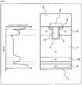
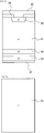
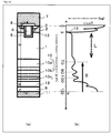
- Fig. 1 is a cross-sectional view illustrating an example of the semiconductor device manufactured by the semiconductor device manufacturing method according to Embodiment 1.
- An impurity concentration distribution in a depth direction of a semiconductor substrate from the boundary between an emitter electrode (first main electrode) 7 and an n ++ emitter region 3 is illustrated on the left side of Fig. 1 .
- a p base region 2 is provided in a surface layer of a front surface of the semiconductor substrate which will be an n - drift layer 1.
- the n ++ emitter region 3 is selectively provided in the p base region 2 so as to be exposed from the front surface of the semiconductor substrate.
- the impurity concentration of the n ++ emitter region 3 is higher than the impurity concentration of the n - drift layer 1.
- a trench 4 is provided so as to reach the n - drift layer 1 through the n ++ emitter region 3 and the p base region 2.
- a gate insulating film 5 is provided along the side wall and bottom of the trench 4. In the trench 4, a gate electrode 6 is provided inside the gate insulating film 5 so as to be buried in the trench 4.
- the emitter electrode 7 comes into contact with the p base region 2 and the n ++ emitter region 3.
- the emitter electrode 7 is electrically insulated from the gate electrode 6 by an interlayer insulating film 8.
- a p + collector layer 9 (first semiconductor layer) is provided in a surface layer of a rear surface of the semiconductor substrate which will be the n - drift layer 1 and an n + field stop layer 10 (second semiconductor layer) is provided in a region which is deeper than the p + collector layer 9 from the rear surface.
- a collector electrode (output electrode) 11 comes into contact with the p + collector layer 9.
- the impurity concentration of the p + collector layer 9 is high enough to obtain an ohmic contact with the collector electrode 11.
- the n + field stop (FS) layer 10 extends in a direction perpendicular to the depth direction of the semiconductor substrate so as to be substantially parallel to the p + collector layer 9.
- the n + field stop (FS) layer 10 is formed with a uniform thickness.
- the n + field stop layer 10 may be separated from the p + collector layer 9 or it may come into contact with the p + collector layer 9.
- the impurity concentration of the n + field stop layer 10 is higher than the impurity concentration of the n - drift layer 1.
- the n + field stop layer 10 is a semiconductor layer to which a hydrogen induced donor is introduced by proton irradiation. Since the hydrogen induced donor forming the semiconductor layer is a composite defect, it has a function which accelerates the recombination of carriers.
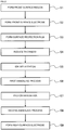
- Fig. 2 is a flowchart illustrating the outline of the semiconductor device manufacturing method according to Embodiment 1.
- each of the above-mentioned semiconductor regions for example, the p base region 2 and the n ++ emitter region 3
- a MOS gate structure for example, the MOS gate structure
- the interlayer insulating film 8 are formed on the front surface side of the semiconductor substrate (Step S1).
- a front surface electrode is formed on the front surface of the semiconductor substrate (Step S2).
- a surface protection film is formed on the front surface of the semiconductor substrate (Step S3).
- the rear surface of the semiconductor substrate is removed by, for example, grinding or etching so that the thickness of the semiconductor substrate is uniformly reduced (the semiconductor substrate is uniformly thinned) (Step S4).
- Step S7 proton irradiation for forming the field stop layer is performed for the rear surface of the semiconductor substrate.
- the proton irradiation is performed in Step S7 with sufficient irradiation energy to enable a proton to be radiated to a position deeper than the semiconductor layer which comes into contact with the rear surface electrode.
- the proton which is radiated in Step S7 is activated (changed into a donor) by a second annealing process (Step S8). In this way, the field stop layer is formed in a deep region of the semiconductor substrate which is disposed on the rear surface.
- the temperature of the second annealing process in Step S8 be set to such an extent that the lattice defects formed by the proton irradiation are not reduced.
- the rear surface electrode is formed on the rear surface of the semiconductor substrate by a physical vapor deposition method such as a sputtering method (Step S9). In this way, the semiconductor device according to Embodiment 1 is completed.
- a series of Step S7 and Step S8 may be performed a plurality of times while changing the irradiation energy and the annealing temperature to form a plurality of stripe-shaped field stop layers which extend in the direction perpendicular to the depth direction of the semiconductor substrate.
- the second annealing process for forming each field stop layer is performed at an annealing temperature that is most suitable to activate the proton radiated in the previous proton irradiation process.
- the second annealing processes for forming the plurality of field stop layers are performed in descending order of the annealing temperature. Adjacent field stop layers may come into contact with each other or they may be separated from each other.
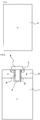
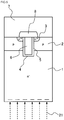
- FIGs. 3 to 8 are cross-sectional views illustrating the semiconductor device according to Embodiment 1 which is being manufactured.
- the semiconductor substrate which will be the n - drift layer 1 is prepared.
- a trench-gate-type MOS gate structure including the p base region 2, the n ++ emitter region 3, the trench 4, the gate insulating film 5, and the gate electrode 6 is formed on the front surface of the semiconductor substrate by a general method.
- an aluminum silicon (AlSi) film which will be the emitter electrode 7 is deposited on the front surface of the semiconductor substrate by sputtering. Then, the aluminum silicon film is patterned to form a wiring pattern and annealing is performed. In this way, the emitter electrode 7 is formed on the front surface of the semiconductor substrate. Then, for example, a polyimide film which will be a surface protection film (not illustrated) is formed on the front surface of the semiconductor substrate so as to cover the emitter electrode 7. Then, the polyimide film is patterned such that a portion of the emitter electrode 7 is exposed. Then, the polyimide film is cured (burned). Then, the rear surface of the semiconductor substrate is ground to reduce the thickness of the semiconductor substrate and the semiconductor substrate is cleaned to remove adhesive materials.
- AlSi aluminum silicon
- p-type impurity ions 21, such as boron ions (B + ), are implanted into the ground rear surface of the semiconductor substrate.
- the ion implantation is performed with a sufficiently high dose to obtain an ohmic contact with the collector electrode 11 which will be formed in the subsequent step.
- the dose of boron ions, which are the p-type impurity ions 21, is equal to or greater than 1 ⁇ 10 13 /cm 2 and equal to or less than 1 ⁇ 10 16 /cm 2 . In Example 1 which will be described below, the dose was 3 ⁇ 10 13 /cm 2 .
- furnace annealing is performed as the first annealing process to activate the p-type impurity ions 21 implanted into the rear surface of the semiconductor substrate, thereby forming the p + collector layer 9 in the surface layer of the rear surface of the semiconductor substrate.
- the temperature of the first annealing process was, for example, 450°C.
- a proton 22 is radiated to a region that is deeper than the p + collector layer 9 from the rear surface of the semiconductor substrate.
- a typical average range Rp is equal to or greater than 5 ⁇ m and equal to or less than 300 ⁇ m.
- the irradiation energy of the proton 22 is equal to or greater than about 0.4 MeV and equal to less than about 6.0 MeV so as to correspond to the average range Rp.
- the irradiation energy of the proton 22 was 0.83 MeV when the average range Rp was, for example, 12 ⁇ m.
- the dose of the proton 22 is typically equal to or greater than 1 ⁇ 10 12 /cm 2 and equal to or less than 1 ⁇ 10 16 /cm 2 .
- the dose was 1 ⁇ 10 13 /cm 2 .
- furnace annealing is performed as the second annealing process to activate the proton 22 radiated to the rear surface of the semiconductor substrate, thereby forming the n + field stop layer 10 in a region that is deeper than the p + collector layer 9 from the rear surface of the semiconductor substrate.
- the temperature of the second annealing process was, for example, 350°C.
- the first annealing process be performed at a sufficiently high temperature not to have an adverse effect on the electrical characteristics of the emitter electrode 7.
- the emitter electrode 7 is made of, for example, a metal material having aluminum (Al) as a main component
- the first annealing process be performed in a temperature range of 420°C to about the melting point of aluminum.
- the melting point of aluminum is about 660°C, for example, in the case of an alloy in which 1% by weight of silicon is included in aluminum.
- the temperature of the second annealing process be set to such an extent that the lattice defects formed by the proton irradiation are not reduced.
- the second annealing process may be performed at a temperature of about 300°C to 500°C under the conditions that the temperature is not higher than the temperature of the first annealing process.
- the temperature of the first annealing process is in the range of 420°C to 500°C
- the temperature of the second annealing is lower than the temperature of the first annealing process.
- the processing time may be in the range of 0.5 hours to 10 hours.
- the temperature of the second annealing process is preferably in the range of 380°C to 450°C and more preferably in the range of 400°C or 420°C, which is lower than the temperature of the first annealing.
- the second annealing process and a metal annealing process which will be described below, are performed at the same annealing temperature, they may be performed at the same time.
- a series of the proton irradiation process and the second annealing process is repeatedly performed to form a plurality of stripe-shaped field stop layers which extend in the direction perpendicular to the depth direction of the semiconductor substrate, the second annealing processes are performed in descending order of the annealing temperature.
- the second annealing process which is performed in a first stage among the plurality of second annealing processes and the first annealing process are performed at the same annealing temperature
- the second annealing process which is performed in the first stage and the first annealing process may be performed at the same time.
- the second annealing process which is performed in the last stage among the plurality of second annealing processes and the metal annealing process which will be described below, are performed at the same annealing temperature
- the second annealing process and the metal annealing process may be performed at the same time.
- a hydrogen fluoride (HF) treatment for reducing contact resistance with a silicon (Si) semiconductor layer and an aluminum film is performed as preprocessing for forming the collector electrode 11 in which a metal film having aluminum as a main component is laminated as a first layer.
- a hydrogen fluoride (HF) treatment for reducing contact resistance with a silicon (Si) semiconductor layer and an aluminum film is performed as preprocessing for forming the collector electrode 11 in which a metal film having aluminum as a main component is laminated as a first layer.
- Fig. 1 aluminum, titanium (Ti), nickel (Ni), and gold (Au) are sequentially deposited on the rear surface of the semiconductor substrate by, for example, sputtering to form the collector electrode 11 in which the four metal films are laminated.
- the metal annealing process for improving the surface formability of the collector electrode 11 is performed. In this way, the trench gate IGBT illustrated is completed.
- the first annealing process can be performed at a higher annealing temperature than the second annealing process. Therefore, the first annealing process can be performed at the annealing temperature which is suitable to activate the p-type impurities that are implanted at a sufficiently high dose (for example, about 1 ⁇ 10 16 /cm 3 ) to form an ohmic contact with the collector electrode.
- the first and second annealing processes at the annealing temperature which is most suitable for both the p + collector layer and the n + field stop layer.
- the p + collector layer so as to come into ohmic contact with the collector electrode and to form the n + field stop layer with a desired hydrogen induced donor concentration.
- a semiconductor device manufacturing method according to Embodiment 2 differs from the semiconductor device manufacturing method according to Embodiment 1 in that the emitter electrode 7 is formed after the second annealing process for forming the n + field stop layer 10.
- a semiconductor device manufactured by the semiconductor device manufacturing method according to Embodiment 2 is the same as the trench gate IGBT according to Embodiment 1 illustrated in Fig. 1 .
- Figs. 9 to 12 are cross-sectional views illustrating the semiconductor device according to Embodiment 2 which is being manufactured.
- a semiconductor substrate which will be an n - drift layer 1 is prepared and a trench-gate-type MOS gate structure is formed on the front surface of the semiconductor substrate.
- the rear surface of the semiconductor substrate is ground and the semiconductor substrate is cleaned to remove adhesive materials.
- p-type impurity ions 21 are implanted into the ground rear surface of the semiconductor substrate and a first annealing process is performed to form a p + collector layer 9.
- a proton 22 is radiated to a region that is deeper than the p + collector layer 9 from the rear surface of the semiconductor substrate and a second annealing process is performed to form an n + field stop layer 10.
- an emitter electrode 7 and a collector electrode 11 are formed on the front and rear surfaces of the semiconductor substrate, respectively. In this way, the trench gate IGBT illustrated in Fig. 1 is completed.
- the first annealing process can be performed before the emitter electrode is formed on the front surface of the semiconductor substrate. Therefore, the first annealing process can be performed at a high annealing temperature of, for example, 900°C or more. As a result, it is possible to further increase the impurity concentration of the p + collector layer and to reduce the contact resistance between the p + collector layer and the collector electrode.
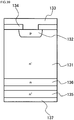
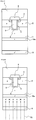
- Fig. 13 is a cross-sectional view illustrating an example of a semiconductor device manufactured by a semiconductor device manufacturing method according to Embodiment 3.
- the semiconductor device manufacturing method according to Embodiment 3 differs from the semiconductor device manufacturing method according to Embodiment 1 in that a diode is manufactured instead of the IGBT.
- a p + anode region 32 is selectively provided in a surface layer of a front surface of an n - semiconductor substrate 31.
- Reference numeral 34 indicates an interlayer insulating film.
- An anode electrode (input electrode) 33 comes into contact with the p + anode region 32.
- an n + cathode layer (first semiconductor layer) 35 is provided in a surface layer of a rear surface of the n - semiconductor substrate 31 and an n + field stop layer 36 is provided in a region that is deeper than the n + cathode layer 35 from the rear surface.
- the n + field stop layer 36 has the same structure as the n + field stop layer according to Embodiment 1.
- a cathode electrode (output electrode) 37 comes into contact with the n + cathode layer 35.
- the impurity concentration of the n + cathode layer 35 is high enough to obtain an ohmic contact with the cathode electrode 37.
- Figs. 14 to 19 are cross-sectional views illustrating the semiconductor device according to Embodiment 3 which is being manufactured.
- the n - semiconductor substrate 31 is prepared.
- the p + anode region 32 is formed in the front surface of the semiconductor substrate 31 by a general method.
- the anode electrode 33 is formed on the front surface of the semiconductor substrate 31 by sputtering.
- the rear surface of the semiconductor substrate 31 is ground and the semiconductor substrate 31 is cleaned to remove adhesive materials.
- n-type impurity ions 23 are implanted into the ground rear surface of the semiconductor substrate and a first annealing process is performed to form the n + cathode layer 35.
- a proton 22 is radiated to a region that is deeper than the n + cathode layer 35 from the rear surface of the semiconductor substrate and a second annealing process is performed to the n + field stop layer 36.
- the cathode electrode 37 is formed on the rear surface of the semiconductor substrate. In this way, the diode illustrated in Fig. 13 is completed.
- Embodiment 3 it is possible to obtain the same effect as that in Embodiment 1. According to Embodiment 3, even when a diode is formed, it is possible to form the n + cathode layer so as to come into ohmic contact with the cathode electrode. In addition, it is possible to form the n + field stop layer with a desired hydrogen induced donor concentration.
- a semiconductor device manufacturing method according to Embodiment 4 differs from the semiconductor device manufacturing method according to Embodiment 3 in that the anode electrode 33 is formed after the second annealing process for forming the n + field stop layer 36.
- a semiconductor device manufactured by the semiconductor device manufacturing method according to Embodiment 4 is the diode illustrated in Fig. 13 which is given an example of the semiconductor device in Embodiment 3.
- Figs. 20 to 23 are cross-sectional views illustrating the semiconductor device according to Embodiment 4 which is being manufactured.
- a semiconductor substrate 31 is prepared and a p + anode region 32 is formed in a front surface of the semiconductor substrate 31.
- a rear surface of the semiconductor substrate 31 is ground and the semiconductor substrate 31 is cleaned to remove adhesive materials.
- the first annealing process can be performed before the anode electrode is formed on the front surface of the semiconductor substrate. Therefore, the first annealing can be performed at a high annealing temperature of, for example, 900°C or more. As a result, it is possible to further increase the impurity concentration of the n + cathode layer and to reduce the contact resistance between the n + cathode layer and the cathode electrode.
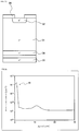
- Fig. 24 is a characteristic diagram illustrating the carrier concentration distribution of a semiconductor device according to an example.
- Fig. 25 is a characteristic diagram illustrating the carrier concentration distribution of a semiconductor device according to the related art.
- the horizontal axis indicates the depth from the boundary between the rear surface electrode and the semiconductor layer which comes into contact with the rear surface electrode.
- the vertical axis indicates carrier concentration, which is obtained by calculating specific resistance from the spreading resistance measured by a known spreading resistance profiling method and converting the specific resistance into carrier concentration.
- the carrier concentration can be regarded as the doping concentration of doped impurities (electrically activated concentration).
- An ion implantation process (Step S5) and a first annealing process (Step S6) for forming a semiconductor layer which came into contact with a rear surface electrode were performed and a proton irradiation process (Step S7) and a second annealing process (Step S8) were performed according to the semiconductor device manufacturing method according to Embodiment 1 to prepare a sample (hereinafter, referred to as an example).
- a proton irradiation process for forming a field stop layer was performed, an ion implantation process for forming a semiconductor layer which came into contact with a rear surface electrode was performed, and a thermal annealing process was collectively performed to prepare a sample (hereinafter, referred to as a comparative example).
- the temperature of the thermal annealing process in the comparative example was equal to the temperature of the second annealing process in the example such that the carrier concentration of the field stop layer was equal to the carrier concentration of the field stop layer in the example.
- impurity concentration was measured in the depth direction from the boundary between the rear surface electrode and the semiconductor layer which came into contact with the rear surface electrode.
- the result illustrated in Fig. 24 proved that, in the example, it was possible to increase the impurity concentration of the rear surface electrode and a semiconductor layer 41 which came into contact with the rear surface electrode since the temperature of the first annealing process for the rear surface electrode and a semiconductor layer 41 which came into contact with the rear surface electrode could be set to be higher than the activation conditions of protons.
- the result illustrated in Fig. 25 proved that, in the comparative example, the impurity concentration of the rear surface electrode and a semiconductor layer 42 which came into contact with the rear surface electrode was low since the upper limit of the annealing temperature of the rear surface electrode and the semiconductor layer 42 which came into contact with the rear surface electrode was determined by the activate conditions of protons.
- Fig. 45 is a cross-sectional view illustrating an example of a semiconductor device manufactured by a semiconductor device manufacturing method according to Embodiment 5.
- Fig. 47 is a characteristic diagram illustrating a carrier concentration distribution of an n + field stop layer in the semiconductor device illustrated in Fig. 45 .
- Fig. 47 illustrates the carrier concentration distribution measured by an SR method. Since a p + collector layer 9 has a very small depth of about 0.5 ⁇ m with respect to the horizontal axis scale of Fig. 47 , the illustration thereof is omitted.
- the semiconductor device manufacturing method according to Embodiment 5 differs from the semiconductor device manufacturing method according to Embodiment 1 in that a plurality of n + field stop layers 10 are formed by a plurality of proton irradiation stages after a first ion implantation process for implanting p-type impurity ions 21, such as boron ions and a first annealing process are performed to form a p + collector layer 9 in the rear surface of a substrate rear.
- the semiconductor device manufactured by the semiconductor device manufacturing method according to Embodiment 5 includes n + field stop layers 10a to 10c with different depths from the rear surface of the substrate.
- the n + field stop layers 10a to 10c are provided so as to be separated from each other. As the depth of the n + field stop layers from the rear surface of the substrate increases, the carrier concentration thereof is reduced.
- the n + field stop layer 10c which is provided at the shallowest position from the rear surface of the substrate is arranged so as to be separated from the p + collector layer 9.
- Figs. 48 to 52 are cross-sectional views illustrating the semiconductor device according to Embodiment 5 which is being manufactured.
- a semiconductor substrate which will be an n - drift layer 1 is prepared and a trench-gate-type MOS gate structure and an emitter electrode 7 are formed on the front surface of the semiconductor substrate.
- the rear surface of the semiconductor substrate is ground and the semiconductor substrate is cleaned to remove adhesive materials.
- p-type impurity ions 21 are implanted into the ground rear surface of the semiconductor substrate and the first annealing process is performed to form the p + collector layer 9.
- a first proton irradiation process is performed to introduce a proton 51 to a region that is deeper than the p + collector layer 9 from the rear surface of the semiconductor substrate.
- a second annealing process (hereinafter, referred to as a first-stage second annealing process) is performed for the proton 51 introduced by the first proton irradiation process to form the n + field stop layer 10a.
- the n + field stop layer 10a is formed at a depth of, for example, 60 ⁇ m from the rear surface of the substrate.
- the acceleration energy of the first proton irradiation process may be, for example, 2.3 MeV and the dose of the proton 51 may be, for example, 1 ⁇ 10 14 /cm 2 .
- the first-stage second annealing process may be performed under the conditions of, for example, a temperature of 420°C and 1 hour.
- a second proton irradiation process is performed to introduce a proton 52 to a region that is deeper than the p + collector layer 9 and is shallower than the n + field stop layer 10a from the rear surface of the semiconductor substrate.
- the second annealing process (hereinafter, referred to as a second-stage second annealing process) is performed for the proton 52 introduced by the second proton irradiation process to form the n + field stop layer 10b.
- the n + field stop layer 10b is formed at a depth of, for example, 30 ⁇ m from the rear surface of the substrate.
- the acceleration energy of the second proton irradiation process may be, for example, 1.5 MeV and the dose of the proton 52 may be, for example, 1 ⁇ 10 15 /cm 2 .
- the second-stage second annealing process may be performed under the conditions of, for example, a temperature of 400°C and 1 hour.
- a third proton irradiation process is performed to introduce a proton 53 to a region that is deeper than the p + collector layer 9 and is shallower than the n + field stop layer 10b from the rear surface of the semiconductor substrate.
- the second annealing process (hereinafter, referred to as a third-stage second annealing process) is performed for the proton 53 introduced by the third proton irradiation process to form the n + field stop layer 10c, as illustrated in Fig. 45 .
- the n + field stop layer 10c is formed at a depth of, for example, 5 ⁇ m from the rear surface of the substrate.
- the acceleration energy of the third proton irradiation process may be, for example, 0.45 MeV and the dose of the proton 53 may be, for example, 5 ⁇ 10 15 /cm 2 .
- the third-stage second annealing process may be performed under the conditions of, for example, a temperature of 380°C and 1 hour.
- the first to third proton irradiation processes be sequentially performed at the deep position from the rear surface of the substrate and the temperature of the first-stage to third-stage second annealing processes be reduced as the depth from the rear surface of the substrate is reduced.
- the temperature of the first-stage to third-stage second annealing processes may be in the range of 380°C to 450°C.
- the first-stage to third-stage second annealing processes may be collectively performed after the third proton irradiation process.
- the temperature of the second annealing process be equal to the temperature of the first-stage second annealing process which is performed at the highest temperature.
- a collector electrode 11 is formed on the rear surface of the semiconductor substrate.
- the trench gate IGBT illustrated in Fig. 45 is completed.
- an n buffer layer 12 may be formed before the proton irradiation process (for example, when the p + collector layer 9 is formed).
- Fig. 46 illustrates another example of the semiconductor device manufactured by the semiconductor device manufacturing method according to Embodiment 5.
- Fig. 46 is a cross-sectional view illustrating another example of the semiconductor device manufactured by the semiconductor device manufacturing method according to Embodiment 5.
- Embodiment 5 may be applied to Embodiment 3 to manufacture a diode including a plurality of n + field stop layers 36 (for example, n + field stop layers 36a to 36c), as illustrated in Fig. 46 .
- the structure and forming method of the n + field stop layers 36a to 36c are the same as those of the n + field stop layers 10a to 10c illustrated in Fig. 45 .
- structures other than the plurality of n + field stop layers 36 are the same as those in Embodiment 3.
- Embodiment 5 it is possible to obtain the same effect as that in Embodiment 1.
- Embodiment 5 it is possible to form a plurality of (three) field stop layers including hydrogen donors without a disorder.
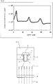
- Fig. 42 is a characteristic diagram illustrating the turn-off oscillation waveform of a general IGBT.
- a collector current is equal to or less than a tenth of a rated current, oscillation is likely to occur before turn-off ends since the number of stored carriers is small.
- the collector current is fixed to a given value and the IGBT is turned off by a different power supply voltage V CC .
- the voltage is greater than the peak value of a general overshoot voltage in a voltage waveform between the collector and the emitter and then an additional overshoot occurs. Then, the additional overshoot (voltage) triggers the oscillation of the subsequent waveform.
- an addition overshoot voltage further increases and the amplitude of the subsequent oscillation increases.
- a threshold voltage at which the voltage waveform starts to oscillate is referred to as an oscillation start threshold value V RRO .
- the oscillation start threshold value V RRO increases, the possibility of the IGBT oscillating when the IGBT is turned off is reduced, which is preferable.
- the oscillation start threshold value V RRO depends on the position of a first proton peak (closest to a p base region) which a depletion layer (strictly, a space-charge region since there is a hole), which is spread from a pn junction between the p base region and an n - drift layer of the IGBT to an n - drift layer, reaches first.
- the reason is as follows.
- the depletion layer is spread from the pn junction between the p base region and the n - drift layer to the n drift layer at the time the IGBT is turned off, the end of the depletion layer reaches the first field stop layer (closest to the p base region) and the spreading of the depletion layer is suppressed. Therefore, the sweep of the stored carriers is weakened. As a result, the depletion of carriers is suppressed and oscillation is suppressed.
- the depletion layer is spread in the depth direction from the pn junction between the p base region and the n - drift layer to the collector electrode. Therefore, the peak position of the field stop layer which the end of the depletion layer reaches first is the field stop layer which is closest to the pn junction between the p base region and the n drift layer.
- the thickness of an n semiconductor substrate (the thickness of a portion interposed between the emitter electrode and the collector electrode) is W 0 and the depth of the peak position of the field stop layer which the end of the depletion layer reaches first from the interface between the collector electrode and the rear surface of the n semiconductor substrate (hereinafter, referred to as a distance from the rear surface) is X.
- a distance index L is introduced.
- the distance index L represented by the above-mentioned Expression (3) is an index indicating the distance of the end of the depletion layer (exactly, a space-charge region) (depletion layer end), which is spread from the pn junction between the p base region and the n - drift layer to the n - drift layer 1, from the pn junction when a voltage V CE between the collector and the emitter that increases at the time the IGBT is turned off is equal to the power supply voltage V CC .
- a denominator indicates the space-charge density of the space-charge region (depletion layer) when the IGBT is turned off.
- q is an elementary charge
- p hole concentration
- n electron concentration
- N d donor concentration
- N a acceptor concentration
- ⁇ s is the permittivity of a semiconductor.
- the donor concentration N d is average concentration obtained by integrating the n drift layer in the depth direction and dividing the integrated value by the length of the integration section.
- the space-charge density ⁇ is described by the hole concentration p in the space-charge region (depletion layer) when the IGBT is turned off and the average donor concentration N d of the n - drift layer.
- the space-charge density ⁇ can be represented by ⁇ q(p+N d ) since the electron concentration is negligibly less than the space-charge density ⁇ and there is no acceptor.
- the hole concentration p is determined by a breaking current of the IGBT.
- the length x of the space-charge region when the voltage V is half of the rated voltage V rate is the distance index L. The reason is that, in the actual device, such as an inverter, an operating voltage (power supply voltage V CC ), which is the voltage V, is about half of the rated voltage V.
- the field stop layer When the doping concentration of the field stop layer is higher than that of the n - drift layer, the field stop layer has a function of making it difficult for the space-charge region to be spread when the IGBT is turned off.
- the collector current of the IGBT starts to be reduced from the breaking current due to the turn-on of a MOS gate
- the peak position of the field stop layer which the depletion layer reaches first is in the range of the length of the space-charge region, it is possible to suppress the spreading of the space-charge region, with the stored carriers remaining in the n - drift layer. Therefore, the sweep of the remaining carriers is suppressed.
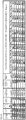
- Fig. 44 is a table illustrating the position conditions of the field stop layer which the depletion layer reaches first in the semiconductor device according to the invention.
- Fig. 44 illustrates the distance X of the peak position of the field stop layer which the end of the depletion layer reaches first from the rear surface at a rated voltage V rate of 600 V to 6500 V.
- X W0 - yL is established ( ⁇ is a coefficient).
- Fig. 44 illustrates the distance X when the coefficient ⁇ is changed from, for example, 0.7 to 1.6.
- the safe design is made at each rated voltage such that the element (IGBT) has a breakdown voltage that is about 10 percent higher than the rated voltage.
- the total thickness of the n semiconductor substrate (the thickness of the n semiconductor substrate during a finishing process after the semiconductor substrate is thinned by, for example, grinding) and the average specific resistance of the n - drift layer 1 are set such that an on-voltage or turn-off loss is sufficiently reduced.
- the term "average” means the average concentration and specific resistance of the entire n - drift layer 1 including the field stop layer.
- the rated current density J F has a typical value, depending on the rated voltage.
- the rated current density J F is set such that energy density which is determined by the product of the rated voltage and the rated current density J F is substantially constant and substantially has the value illustrated in Fig. 44 .
- the distance index L is calculated by the above-mentioned Expression (3) on the basis of these values, the value illustrated in Fig. 44 is obtained.
- the distance X of the peak position of the field stop layer which the end of the depletion layer reaches first from the rear surface is obtained by subtracting the value of ⁇ , which is in the range of 0.7 to 1.6 with respect to the distance index L, from the thickness W 0 of the n semiconductor substrate.
- Fig. 41 is a characteristic diagram illustrating a threshold voltage at which the voltage waveform starts to oscillate.
- Fig. 41 illustrates the dependence of the oscillation start threshold value V RRO on ⁇ at some typical rated voltages V rate (600 V, 1200 V, and 3300 V).
- the vertical axis indicates a value obtained by normalizing the oscillation start threshold value V RRO with the rated voltage V rate .
- the range of ⁇ which can sufficiently increase the oscillation start threshold value V RRO is substantially the same (for example, 0.7 to 1.4) at any rated voltage V rate .
- the distance (depth) of the end of the space-charge region is equal to about the distance index L represented by the above-mentioned Expression (3).
- the peak position of the field stop layer which is disposed at the deepest position from the rear surface is aligned with the position of the distance index L (that is, ⁇ is about 1.0)
- the distance index L is greater than 20 ⁇ m at any rated voltage V rate . That is, the range Rp of protons for forming the first proton peak, which is disposed at the deepest position from the rear surface of the substrate, from the rear surface of the substrate is greater than 15 ⁇ m, particularly, equal to or deeper than 20 ⁇ m from the rear surface of the substrate in order to maximize the oscillation inhibitory effect.
- the acceleration energy of a proton in the semiconductor device manufacturing method according to the invention will be described as Example 3.
- the acceleration energy of the proton may be determined from the characteristic diagram illustrated in Fig. 43 , which will be described below, in order to actually form the field stop layer using proton irradiation such that the peak position of the field stop layer which a depletion layer reaches first has a distance X from the rear surface of a substrate and the above-mentioned range of ⁇ is satisfied.
- Fig. 43 is the characteristic diagram illustrating the relationship between the average range of the proton and the acceleration energy of the proton in the semiconductor device according to the invention.
- Fig. 43 is the characteristic diagram illustrating the above-mentioned Expression (4) and illustrates the acceleration energy of the proton for obtaining the desired average range Rp of the proton.
- the horizontal axis indicates the logarithm log(Rp) of the average range Rp of the proton and a corresponding average range Rp ( ⁇ m) is described in parentheses below the axis value of log(Rp).
- the vertical axis indicates the logarithm log(E) of the acceleration energy E of the proton and the corresponding acceleration energy E of the proton is described in parentheses on the left side of the axis value of log(E).
- the acceleration energy E of proton irradiation is calculated (hereinafter, referred to as a calculated value E) from the desired average range Rp of the proton by the above-mentioned fitting expression and the proton is implemented into a silicon substrate with the calculated value E of the acceleration energy
- the relationship between the actual acceleration energy E' and the average range Rp' (proton peak position) which is actually obtained by a spreading resistance (SR) profiling method may be considered as follows.
- the actual average range Rp' is in the range of about ⁇ 10% of the desired average range Rp, which is in a measurement error range. Therefore, the influence of the deviation of the actual average range Rp' from the desired average range Rp on the electrical characteristics of a diode or an IGBT is small enough to be negligible.
- the actual average range Rp' can be determined to be substantially equal to the set average range Rp.
- the actual average range Rp' may be in the range of ⁇ 10% of the average range Rp which is calculated by substituting the actual acceleration energy E' into the above-mentioned Expression (4).
- the acceleration energy E and the average range Rp are within the above-mentioned ranges ( ⁇ 10%), it is considered that the actual acceleration energy E' and the actual average range Rp' follow the fitting expression illustrated in the above-mentioned Expression (4) which is represented by the desired average range Rp and the calculated value E and no problem occurs.
- the range of a variation or an error may be in the range of ⁇ 10% of the average range Rp. It is preferable that the range of the variation or the error be in the range of ⁇ 5% of the average range Rp. In this case, it can be considered that the actual acceleration energy E' and the actual average range Rp' perfectly follow the above-mentioned Expression (4).
- the use of the above-mentioned Expression (4) makes it possible to calculate the acceleration energy E of the proton required to obtain the desired average range Rp of the proton.
- the acceleration energy E of each proton for forming the field stop layer is substantially equal to a measured value obtained by actually measuring a sample, which is irradiated with protons with the acceleration energy E', using the spreading resistance (SR) profiling method. Therefore, the use of the above-mentioned Expression (4) makes it possible to estimate the required acceleration energy E of the proton with high accuracy on the basis of the average range Rp of the proton.
- a semiconductor device manufacturing method differs from the semiconductor device manufacturing method according to Embodiment 1 in that a laser annealing process 61 is performed as the first annealing process which is performed after the first ion implantation process for implanting p-type impurity ions 21, such as boron ions, in order to form the p + collector layer 9 in the rear surface of the substrate.
- An n + field stop layer 10 may be provided by one proton irradiation process as in Embodiment 1 or a plurality of n + field stop layers 10 may be provided by a plurality of proton irradiation processes as in Embodiment 5.
- Fig. 53 is a cross-sectional view illustrating a semiconductor device according to Embodiment 6 which is being manufactured.
- a semiconductor substrate which will be an n - drift layer 1 is prepared and a trench-gate-type MOS gate structure and an emitter electrode 7 are formed on a front surface of the semiconductor substrate.
- a rear surface of the semiconductor substrate is ground and the semiconductor substrate is cleaned to remove adhesive materials.
- the p-type impurity ions 21 are implanted into the ground rear surface of the semiconductor substrate.
- the laser annealing process 61 is performed as a first annealing process to form a p + collector layer 9 in a surface layer of the rear surface of the semiconductor substrate, as illustrated in Fig. 6 .
- a proton 22 is radiated to a region that is deeper from the p + collector layer 9 from the rear surface of the semiconductor substrate and a furnace annealing process is performed as a second annealing process to form an n + field stop layer 10.
- a collector electrode 11 is formed on the rear surface of the semiconductor substrate. In this way, the trench gate IGBT illustrated in Fig. 1 is completed.
- Embodiment 6 it is possible to obtain the same effect as that in Embodiment 1.
- the n + field stop layer is not affected by the laser annealing process for forming the p + collector layer.
- the hydrogen donor concentration of the third (with an average range Rp of, for example, 5 ⁇ m) n + field stop layer which is formed at the position close to the p + collector layer is not reduced by the laser annealing process. Therefore, it is possible to maintain the concentration of the n + field stop layer at a high level. As a result, it is possible to prevent the disappearance of the n + field stop layer.
- the invention is not limited to the above-described embodiments, but it is defined by the scope of the claims.
- the invention can be applied to various semiconductor devices in which the field stop layer can be provided.
- the trench gate IGBT is given as an example.
- the invention may be applied to a planar gate IGBT.
- the input electrode (the emitter electrode or the anode electrode) is formed after the second annealing process.
- the input electrode may be formed after the first annealing process. In this case, the same effect as that in Embodiment 2 is obtained.
- a method for introducing impurities to form the semiconductor layers (the collector layer and the cathode layer) which come into contact with the output electrode is not limited to the ion implantation method, but various other methods may be used.
- the first conductivity type is an n type and the second conductivity type is a p type.
- the first conductivity type may be the p type and the second conductivity type may be the n type. In this case, the same effect as described above is obtained.
Landscapes
- Electrodes Of Semiconductors (AREA)
- Physics & Mathematics (AREA)
- Engineering & Computer Science (AREA)
- Plasma & Fusion (AREA)
- Health & Medical Sciences (AREA)
- High Energy & Nuclear Physics (AREA)
- Toxicology (AREA)
Claims (8)
- Procédé pour la fabrication d'un dispositif à semi-conducteurs comprenant une électrode d'entrée (7) fournie sur une surface avant d'un substrat semi-conducteur, qui est un substrat en silicium d'un premier type de conductivité qui un type de conductivité de type n, et une électrode de sortie (11) fournie sur une surface arrière du substrat semi-conducteur, le procédé comprenant:une étape d'introduction, d'introduction d'impuretés dans la surface arrière du substrat semi-conducteur;une première étape de recuit, d'activation des impuretés introduites dans la surface arrière du substrat semi-conducteur en utilisant un premier processus de recuit pour former une première couche semi-conductrice (9), qui est une partie de contact avec l'électrode de sortie (11), dans une couche de surface de la surface arrière du substrat semi-conducteur;une étape d'irradiation, d'irradiation aux protons (22) de la surface arrière du substrat semi-conducteur après la première étape de recuit; etune deuxième étape de recuit, d'activation des protons (22) avec lesquels on a irradié la surface arrière du substrat semi-conducteur en utilisant un deuxième processus de recuit pour former une deuxième couche semi-conductrice (10) du premier type de conductivité, laquelle a une concentration plus élevée d'impuretés que le substrat semi-conducteur, dans une zone qui est plus profonde que la première couche semi-conductrice à partir de la surface arrière du substrat semi-conducteur, dans lequel la première étape de recuit est réalisée à une température de recuit plus élevée que la deuxième étape de recuit,dans lequel l'étape d'irradiation est réalisée une pluralité de fois après la première étape de recuit, et la deuxième étape de recuit est réalisée à chaque fois que l'étape d'irradiation est réalisée, ou la deuxième étape de recuit est réalisée une fois après la dernière étape d'irradiation,dans lequel la première étape de recuit est une étape de recuit au laser,dans lequel la plage des protons formant un premier maximum de protons, qui sont disposés à la position la plus profonde à partir de la surface arrière du substrat, est d'une profondeur supérieure ou égale à 20 µm,dans lequel, dans l'étape d'irradiation, une énergie d'accélération E en eV des protons lorsque la deuxième couche semi-conductrice (10) avec une plage Rp en µm est formée par l'irradiation aux protons satisfait à l'expression (2) suivante :
 où x est un logarithme log(Rp) de la plage Rp, et y est un logarithme log(E) de l'énergie d'accélération E,dans lequel une couche de migration (1) du premier type de conductivité qui est le substrat semi-conducteur est fournie,une troisième couche semi-conductrice (2) d'un deuxième type de conductivité est formée dans la surface avant du substrat semi-conducteur,lorsque q est une charge élémentaire, Nd est la concentration moyenne en donneurs dans la couche de migration (1), εs est la constante diélectrique du substrat semi-conducteur, Vrate en V est une tension nominale, JF est une densité de courant nominal en A/cm2, et Vset est une vitesse saturée à laquelle une vitesse de porteurs est saturée avec une intensité de champ électrique prédéterminée, un indice de distance L en µm est représenté par l'expression (1) suivante :
[équation 1] dans lequel γ est supérieur ou égal à 0,9 et inférieur ou égal à 1,4, oudans lequel γ est supérieur ou égal à 1,0 et inférieur ou égal à 1,3,dans lequel le procédé se caractérise en outre par une étape d'amincissement où le substrat semi-conducteur est rectifié ou décapé à partir d'une surface arrière pour réduire l'épaisseur uniformément, ce qui est fait avant la définition de l'étape d'introduction et l'étape de recuit pour former la première couche semi-conductrice (9).
 - Procédé pour la fabrication d'un dispositif à semi-conducteurs selon la revendication 1, comprenant en outre:une étape de formation d'électrode de sortie, de formation de l'électrode de sortie (11) qui arrive en contact avec la première couche semi-conductrice (9),dans lequel la deuxième étape de recuit est réalisée avant l'étape de formation d'électrode de sortie, ou bien la deuxième étape de recuit et l'étape de formation d'électrode de sortie sont réalisées en même temps.
- Procédé pour la fabrication d'un dispositif à semi-conducteurs selon la revendication 2,
dans lequel la température de la deuxième étape de recuit est supérieure ou égale à 380°C et inférieure ou égale à 450°C. - Procédé pour la fabrication d'un dispositif à semi-conducteurs selon la revendication 1,
dans lequel, dans l'étape d'introduction, les impuretés sont introduites avec une dose suffisante pour obtenir un contact ohmique entre l'électrode de sortie (11) et la première couche semi-conductrice (9). - Procédé pour la fabrication d'un dispositif à semi-conducteurs selon la revendication 1, comprenant en outre:
une étape de formation d'électrode d'entrée, de formation de l'électrode d'entrée (7) sur la surface avant du substrat semi-conducteur après la première étape de recuit. - Procédé pour la fabrication d'un dispositif à semi-conducteurs selon la revendication 1,
dans lequel la deuxième couche semi-conductrice (10) est une couche d'arrêt de champ qui supprime l'étalement d'une couche d'épuisement. - Procédé pour la fabrication d'un dispositif à semi-conducteurs selon l'une quelconque des revendications 1 à 4,
dans lequel le dispositif à semi-conducteurs est un transistor bipolaire à grille isolée,
la première couche semi-conductrice (9) est une couche collectrice d'un deuxième type de conductivité, l'électrode de sortie (11) est une électrode de collecte, ou
dans lequel le dispositif à semi-conducteurs est une diode,
la première couche semi-conductrice (9) est une couche de cathode du premier type de conductivité, et l'électrode de sortie (11) est une électrode cathodique. - Procédé pour la fabrication d'un dispositif à semi-conducteurs selon l'une quelconque des revendications précédentes,
dans lequel la température de la deuxième étape de recuit est supérieure ou égale à 300 °C et inférieure ou égale à 500 °C, ou
dans lequel la température de la deuxième étape de recuit est supérieure ou égale à 300 °C et inférieure ou égale à 380 °C, ou
dans lequel la température de la deuxième étape de recuit est supérieure ou égale à 300 °C et inférieure ou égale à 350 °C, et/ou
dans lequel le temps de recuit de la deuxième étape de recuit est dans la plage de 0,5 heure à 10 heures.
Applications Claiming Priority (2)
| Application Number | Priority Date | Filing Date | Title |
|---|---|---|---|
| JP2012080685 | 2012-03-30 | ||
| PCT/JP2013/059776 WO2013147275A1 (fr) | 2012-03-30 | 2013-03-29 | Procédé de fabrication d'un dispositif à semi-conducteurs |
Publications (3)
| Publication Number | Publication Date |
|---|---|
| EP2793268A1 EP2793268A1 (fr) | 2014-10-22 |
| EP2793268A4 EP2793268A4 (fr) | 2015-08-19 |
| EP2793268B1 true EP2793268B1 (fr) | 2020-06-03 |
Family
ID=49260513
Family Applications (1)
| Application Number | Title | Priority Date | Filing Date |
|---|---|---|---|
| EP13769834.6A Active EP2793268B1 (fr) | 2012-03-30 | 2013-03-29 | Procédé de fabrication d'un dispositif à semi-conducteurs |
Country Status (6)
| Country | Link |
|---|---|
| US (1) | US9466689B2 (fr) |
| EP (1) | EP2793268B1 (fr) |
| JP (3) | JP5880691B2 (fr) |
| KR (1) | KR102023175B1 (fr) |
| CN (1) | CN104054178B (fr) |
| WO (1) | WO2013147275A1 (fr) |
Families Citing this family (38)
| Publication number | Priority date | Publication date | Assignee | Title |
|---|---|---|---|---|
| CN104054178B (zh) * | 2012-03-30 | 2017-09-08 | 富士电机株式会社 | 半导体装置的制造方法 |
| EP2790209B1 (fr) | 2012-03-30 | 2019-09-25 | Fuji Electric Co., Ltd. | Procédé de fabrication pour dispositif à semi-conducteur |
| JP6265594B2 (ja) * | 2012-12-21 | 2018-01-24 | ラピスセミコンダクタ株式会社 | 半導体装置の製造方法、及び半導体装置 |
| JP6037012B2 (ja) * | 2013-06-26 | 2016-11-30 | 富士電機株式会社 | 半導体装置および半導体装置の製造方法 |
| WO2015087507A1 (fr) * | 2013-12-10 | 2015-06-18 | 株式会社アルバック | Transistor bipolaire à grille isolée et son procédé de fabrication |
| US9673308B2 (en) * | 2013-12-13 | 2017-06-06 | Mitsubishi Electric Corporation | Semiconductor device manufacturing method |
| JP6098540B2 (ja) * | 2014-02-10 | 2017-03-22 | トヨタ自動車株式会社 | 半導体装置及び半導体装置の製造方法 |
| CN106062961B (zh) | 2014-09-17 | 2020-02-11 | 富士电机株式会社 | 半导体装置以及半导体装置的制造方法 |
| JP6237921B2 (ja) * | 2014-09-30 | 2017-11-29 | 富士電機株式会社 | 半導体装置および半導体装置の製造方法 |
| CN107710417B (zh) * | 2015-06-16 | 2021-06-11 | 三菱电机株式会社 | 半导体装置的制造方法 |
| CN105321817A (zh) * | 2015-10-26 | 2016-02-10 | 株洲南车时代电气股份有限公司 | 一种二极管及其阴极金属化方法 |
| WO2017086018A1 (fr) * | 2015-11-16 | 2017-05-26 | 富士電機株式会社 | Dispositif à semi-conducteur et son procédé de fabrication |
| US20170210025A1 (en) * | 2016-01-23 | 2017-07-27 | John Bean Technologies Corporation | Disposable cutting blade for blade portioner and mounting system for blade |
| EP3443595B1 (fr) * | 2016-04-11 | 2020-10-07 | ABB Power Grids Switzerland AG | Dispositif semi-conducteur à grille isolée et son procédé de fabrication |
| KR102371864B1 (ko) | 2016-04-27 | 2022-03-07 | 스미도모쥬기가이고교 가부시키가이샤 | 레이저어닐링방법 및 레이저어닐링장치 |
| WO2017197129A1 (fr) * | 2016-05-13 | 2017-11-16 | Farmpod, Llc | Système et procédé de culture aquaponique autonome, modulaire et automatisé |
| DE102016112139B3 (de) * | 2016-07-01 | 2018-01-04 | Infineon Technologies Ag | Verfahren zum Reduzieren einer Verunreinigungskonzentration in einem Halbleiterkörper |
| DE112017003587B4 (de) * | 2016-07-15 | 2024-05-29 | Rohm Co., Ltd. | Halbleitervorrichtung und verfahren zur herstellung einer halbleitervorrichtung |
| CN108604602B (zh) * | 2016-08-12 | 2021-06-15 | 富士电机株式会社 | 半导体装置及半导体装置的制造方法 |
| US10439062B2 (en) * | 2016-09-09 | 2019-10-08 | Infineon Technologies Ag | Metallization layers for semiconductor devices and methods of forming thereof |
| JP6547724B2 (ja) * | 2016-11-15 | 2019-07-24 | トヨタ自動車株式会社 | 半導体装置の製造方法 |
| DE102016122791B3 (de) * | 2016-11-25 | 2018-05-30 | mi2-factory GmbH | Ionenimplantationsanlage, Filterkammer und Implantationsverfahren unter Einsatz eines Energiefilterelements |
| JP6824135B2 (ja) * | 2017-09-29 | 2021-02-03 | 三菱電機株式会社 | 半導体装置及びその製造方法 |
| KR101977957B1 (ko) | 2017-10-30 | 2019-05-13 | 현대오트론 주식회사 | 전력 반도체 소자 및 그 제조방법 |
| DE112019000094T5 (de) | 2018-03-19 | 2020-09-24 | Fuji Electric Co., Ltd. | Halbleitervorrichtung und verfahren zum herstellen einerhalbleitervorrichtung |
| JP7030637B2 (ja) * | 2018-07-23 | 2022-03-07 | 三菱電機株式会社 | 半導体装置の製造方法 |
| CN109712886A (zh) * | 2018-12-17 | 2019-05-03 | 成都森未科技有限公司 | 一种功率半导体器件的背面加工工艺 |
| WO2021029285A1 (fr) | 2019-08-09 | 2021-02-18 | 富士電機株式会社 | Dispositif à semi-conducteur |
| DE112020001029B4 (de) | 2019-10-11 | 2025-06-05 | Fuji Electric Co., Ltd. | Halbleitervorrichtung und herstellungsverfahren einer halbleitervorrichtung |
| CN111725312A (zh) * | 2020-06-05 | 2020-09-29 | 安徽瑞迪微电子有限公司 | 一种高性能半导体功率器件及其制造方法 |
| DE112021000205T5 (de) | 2020-07-15 | 2022-08-18 | Fuji Electric Co., Ltd. | Halbleitervorrichtung |
| JP7528628B2 (ja) * | 2020-08-20 | 2024-08-06 | 三菱電機株式会社 | 半導体装置および半導体装置の製造方法 |
| WO2022107728A1 (fr) * | 2020-11-17 | 2022-05-27 | 富士電機株式会社 | Dispositif à semi-conducteur |
| WO2022196768A1 (fr) * | 2021-03-17 | 2022-09-22 | 富士電機株式会社 | Dispositif semi-conducteur |
| US20230084128A1 (en) * | 2021-09-16 | 2023-03-16 | Hitachi Metals, Ltd. | Silicon carbide substrate and method of manufacturing the same |
| CN113921395A (zh) * | 2021-10-13 | 2022-01-11 | 南瑞联研半导体有限责任公司 | 一种低损耗igbt芯片集电极结构及其制备方法 |
| JP2023172669A (ja) * | 2022-05-24 | 2023-12-06 | 三菱電機株式会社 | 半導体装置及びその製造方法 |
| DE112024001132T5 (de) * | 2023-11-16 | 2026-01-08 | Fuji Electric Co., Ltd. | Halbleitervorrichtung und verfahren zum herstellen der halbleitervorrichtung |
Citations (1)
| Publication number | Priority date | Publication date | Assignee | Title |
|---|---|---|---|---|
| US20110233714A1 (en) * | 2010-03-24 | 2011-09-29 | Fuji Electric Systems Co. Ltd. | Semiconductor device |
Family Cites Families (22)
| Publication number | Priority date | Publication date | Assignee | Title |
|---|---|---|---|---|
| JP3458590B2 (ja) * | 1996-03-27 | 2003-10-20 | 富士電機株式会社 | 絶縁ゲートバイポーラトランジスタ |
| JP3684962B2 (ja) * | 1999-12-01 | 2005-08-17 | 富士電機デバイステクノロジー株式会社 | 半導体装置の製造方法 |
| US6482681B1 (en) * | 2000-05-05 | 2002-11-19 | International Rectifier Corporation | Hydrogen implant for buffer zone of punch-through non epi IGBT |
| JP3951738B2 (ja) | 2001-02-23 | 2007-08-01 | 富士電機デバイステクノロジー株式会社 | 半導体装置の製造方法 |
| DE10207522B4 (de) | 2001-02-23 | 2018-08-02 | Fuji Electric Co., Ltd. | Halbleiterbauelement und Verfahren zu dessen Herstellung |
| JP3764343B2 (ja) | 2001-02-28 | 2006-04-05 | 株式会社東芝 | 半導体装置の製造方法 |
| JP5160001B2 (ja) * | 2001-04-02 | 2013-03-13 | 富士電機株式会社 | 半導体装置の製造方法 |
| JP4539011B2 (ja) * | 2002-02-20 | 2010-09-08 | 富士電機システムズ株式会社 | 半導体装置 |
| DE102004039209B4 (de) | 2004-08-12 | 2009-04-23 | Infineon Technologies Austria Ag | Verfahren zur Herstellung einer n-dotierten Feldstoppzone in einem Halbleiterkörper und Halbleiterbauelement mit einer Feldstoppzone |
| DE102004047749B4 (de) * | 2004-09-30 | 2008-12-04 | Infineon Technologies Austria Ag | Halbleiterbauteil Diode und IGBT sowie dafür geeignetes Herstellungsverfahren |
| DE102005007599B3 (de) | 2005-02-18 | 2006-05-11 | Infineon Technologies Austria Ag | Verfahren zur Herstellung einer Feldstoppzone |
| US7956419B2 (en) | 2005-11-02 | 2011-06-07 | International Rectifier Corporation | Trench IGBT with depletion stop layer |
| JP2007173675A (ja) * | 2005-12-26 | 2007-07-05 | Toyota Central Res & Dev Lab Inc | 半導体装置とその製造方法 |
| JP5228282B2 (ja) * | 2006-03-28 | 2013-07-03 | トヨタ自動車株式会社 | 電力用半導体装置及びその製造方法 |
| US7538412B2 (en) * | 2006-06-30 | 2009-05-26 | Infineon Technologies Austria Ag | Semiconductor device with a field stop zone |
| US7989888B2 (en) * | 2006-08-31 | 2011-08-02 | Infineon Technologies Autria AG | Semiconductor device with a field stop zone and process of producing the same |
| JP5396689B2 (ja) * | 2006-09-07 | 2014-01-22 | 富士電機株式会社 | 半導体装置およびその製造方法 |
| JP5326217B2 (ja) * | 2007-03-15 | 2013-10-30 | 富士電機株式会社 | 半導体装置およびその製造方法 |
| JP5203667B2 (ja) * | 2007-10-16 | 2013-06-05 | トヨタ自動車株式会社 | 半導体装置の製造方法 |
| JP5365009B2 (ja) | 2008-01-23 | 2013-12-11 | 富士電機株式会社 | 半導体装置およびその製造方法 |
| JP5569532B2 (ja) | 2009-11-02 | 2014-08-13 | 富士電機株式会社 | 半導体装置および半導体装置の製造方法 |
| CN104054178B (zh) * | 2012-03-30 | 2017-09-08 | 富士电机株式会社 | 半导体装置的制造方法 |
-
2013
- 2013-03-29 CN CN201380005432.5A patent/CN104054178B/zh active Active
- 2013-03-29 US US14/372,451 patent/US9466689B2/en active Active
- 2013-03-29 KR KR1020147019490A patent/KR102023175B1/ko not_active Expired - Fee Related
- 2013-03-29 JP JP2014508243A patent/JP5880691B2/ja active Active
- 2013-03-29 EP EP13769834.6A patent/EP2793268B1/fr active Active
- 2013-03-29 WO PCT/JP2013/059776 patent/WO2013147275A1/fr not_active Ceased
-
2015
- 2015-09-16 JP JP2015182770A patent/JP6187560B2/ja active Active
-
2017
- 2017-06-07 JP JP2017112525A patent/JP6460153B2/ja active Active
Patent Citations (1)
| Publication number | Priority date | Publication date | Assignee | Title |
|---|---|---|---|---|
| US20110233714A1 (en) * | 2010-03-24 | 2011-09-29 | Fuji Electric Systems Co. Ltd. | Semiconductor device |
Also Published As
| Publication number | Publication date |
|---|---|
| JP2017183749A (ja) | 2017-10-05 |
| JP5880691B2 (ja) | 2016-03-09 |
| JP6187560B2 (ja) | 2017-08-30 |
| KR102023175B1 (ko) | 2019-09-19 |
| CN104054178B (zh) | 2017-09-08 |
| JP6460153B2 (ja) | 2019-01-30 |
| EP2793268A4 (fr) | 2015-08-19 |
| KR20140141572A (ko) | 2014-12-10 |
| US20150024556A1 (en) | 2015-01-22 |
| JPWO2013147275A1 (ja) | 2015-12-14 |
| WO2013147275A1 (fr) | 2013-10-03 |
| JP2016015514A (ja) | 2016-01-28 |
| EP2793268A1 (fr) | 2014-10-22 |
| CN104054178A (zh) | 2014-09-17 |
| US9466689B2 (en) | 2016-10-11 |
Similar Documents
| Publication | Publication Date | Title |
|---|---|---|
| EP2793268B1 (fr) | Procédé de fabrication d'un dispositif à semi-conducteurs | |
| EP2790209B1 (fr) | Procédé de fabrication pour dispositif à semi-conducteur | |
| US10128360B2 (en) | Semiconductor device and method for producing the same | |
| EP2790208B1 (fr) | Procédé de production d'un dispositif à semi-conducteur | |
| EP2782121B1 (fr) | Dispositif semi-conducteur et procédé de fabrication du dispositif semi-conducteur | |
| US10651269B2 (en) | Semiconductor device and method for producing semiconductor device | |
| EP2793251B1 (fr) | Procédé de production d'un dispositif semi-conducteur |
Legal Events
| Date | Code | Title | Description |
|---|---|---|---|
| PUAI | Public reference made under article 153(3) epc to a published international application that has entered the european phase |
Free format text: ORIGINAL CODE: 0009012 |
|
| 17P | Request for examination filed |
Effective date: 20140714 |
|
| AK | Designated contracting states |
Kind code of ref document: A1 Designated state(s): AL AT BE BG CH CY CZ DE DK EE ES FI FR GB GR HR HU IE IS IT LI LT LU LV MC MK MT NL NO PL PT RO RS SE SI SK SM TR |
|
| RIN1 | Information on inventor provided before grant (corrected) |
Inventor name: KURIBAYASHI, HIDENAO Inventor name: MIYAZAKI, MASAYUKI Inventor name: YOSHIMURA, TAKASHI Inventor name: TAKISHITA, HIROSHI |
|
| DAX | Request for extension of the european patent (deleted) | ||
| RA4 | Supplementary search report drawn up and despatched (corrected) |
Effective date: 20150720 |
|
| RIC1 | Information provided on ipc code assigned before grant |
Ipc: H01L 29/739 20060101AFI20150714BHEP Ipc: H01L 21/265 20060101ALI20150714BHEP Ipc: H01L 29/66 20060101ALI20150714BHEP Ipc: H01L 29/08 20060101ALI20150714BHEP Ipc: H01L 29/868 20060101ALI20150714BHEP Ipc: H01L 21/336 20060101ALI20150714BHEP Ipc: H01L 21/329 20060101ALI20150714BHEP Ipc: H01L 29/78 20060101ALI20150714BHEP |
|
| STAA | Information on the status of an ep patent application or granted ep patent |
Free format text: STATUS: EXAMINATION IS IN PROGRESS |
|
| 17Q | First examination report despatched |
Effective date: 20170912 |
|
| GRAP | Despatch of communication of intention to grant a patent |
Free format text: ORIGINAL CODE: EPIDOSNIGR1 |
|
| STAA | Information on the status of an ep patent application or granted ep patent |
Free format text: STATUS: GRANT OF PATENT IS INTENDED |
|
| INTG | Intention to grant announced |
Effective date: 20191213 |
|
| GRAS | Grant fee paid |
Free format text: ORIGINAL CODE: EPIDOSNIGR3 |
|
| GRAA | (expected) grant |
Free format text: ORIGINAL CODE: 0009210 |
|
| STAA | Information on the status of an ep patent application or granted ep patent |
Free format text: STATUS: THE PATENT HAS BEEN GRANTED |
|
| RIN1 | Information on inventor provided before grant (corrected) |
Inventor name: YOSHIMURA, TAKASHI Inventor name: TAKISHITA, HIROSHI Inventor name: MIYAZAKI, MASAYUKI Inventor name: KURIBAYASHI, HIDENAO |
|
| AK | Designated contracting states |
Kind code of ref document: B1 Designated state(s): AL AT BE BG CH CY CZ DE DK EE ES FI FR GB GR HR HU IE IS IT LI LT LU LV MC MK MT NL NO PL PT RO RS SE SI SK SM TR |
|
| REG | Reference to a national code |
Ref country code: GB Ref legal event code: FG4D |
|
| REG | Reference to a national code |
Ref country code: CH Ref legal event code: EP Ref country code: AT Ref legal event code: REF Ref document number: 1277922 Country of ref document: AT Kind code of ref document: T Effective date: 20200615 |
|
| REG | Reference to a national code |
Ref country code: DE Ref legal event code: R096 Ref document number: 602013069628 Country of ref document: DE |
|
| REG | Reference to a national code |
Ref country code: LT Ref legal event code: MG4D |
|
| PG25 | Lapsed in a contracting state [announced via postgrant information from national office to epo] |
Ref country code: FI Free format text: LAPSE BECAUSE OF FAILURE TO SUBMIT A TRANSLATION OF THE DESCRIPTION OR TO PAY THE FEE WITHIN THE PRESCRIBED TIME-LIMIT Effective date: 20200603 Ref country code: GR Free format text: LAPSE BECAUSE OF FAILURE TO SUBMIT A TRANSLATION OF THE DESCRIPTION OR TO PAY THE FEE WITHIN THE PRESCRIBED TIME-LIMIT Effective date: 20200904 Ref country code: LT Free format text: LAPSE BECAUSE OF FAILURE TO SUBMIT A TRANSLATION OF THE DESCRIPTION OR TO PAY THE FEE WITHIN THE PRESCRIBED TIME-LIMIT Effective date: 20200603 Ref country code: SE Free format text: LAPSE BECAUSE OF FAILURE TO SUBMIT A TRANSLATION OF THE DESCRIPTION OR TO PAY THE FEE WITHIN THE PRESCRIBED TIME-LIMIT Effective date: 20200603 Ref country code: NO Free format text: LAPSE BECAUSE OF FAILURE TO SUBMIT A TRANSLATION OF THE DESCRIPTION OR TO PAY THE FEE WITHIN THE PRESCRIBED TIME-LIMIT Effective date: 20200903 |
|
| REG | Reference to a national code |
Ref country code: NL Ref legal event code: MP Effective date: 20200603 |
|
| PG25 | Lapsed in a contracting state [announced via postgrant information from national office to epo] |
Ref country code: RS Free format text: LAPSE BECAUSE OF FAILURE TO SUBMIT A TRANSLATION OF THE DESCRIPTION OR TO PAY THE FEE WITHIN THE PRESCRIBED TIME-LIMIT Effective date: 20200603 Ref country code: BG Free format text: LAPSE BECAUSE OF FAILURE TO SUBMIT A TRANSLATION OF THE DESCRIPTION OR TO PAY THE FEE WITHIN THE PRESCRIBED TIME-LIMIT Effective date: 20200903 Ref country code: HR Free format text: LAPSE BECAUSE OF FAILURE TO SUBMIT A TRANSLATION OF THE DESCRIPTION OR TO PAY THE FEE WITHIN THE PRESCRIBED TIME-LIMIT Effective date: 20200603 Ref country code: LV Free format text: LAPSE BECAUSE OF FAILURE TO SUBMIT A TRANSLATION OF THE DESCRIPTION OR TO PAY THE FEE WITHIN THE PRESCRIBED TIME-LIMIT Effective date: 20200603 |
|
| REG | Reference to a national code |
Ref country code: AT Ref legal event code: MK05 Ref document number: 1277922 Country of ref document: AT Kind code of ref document: T Effective date: 20200603 |
|
| PG25 | Lapsed in a contracting state [announced via postgrant information from national office to epo] |
Ref country code: NL Free format text: LAPSE BECAUSE OF FAILURE TO SUBMIT A TRANSLATION OF THE DESCRIPTION OR TO PAY THE FEE WITHIN THE PRESCRIBED TIME-LIMIT Effective date: 20200603 Ref country code: AL Free format text: LAPSE BECAUSE OF FAILURE TO SUBMIT A TRANSLATION OF THE DESCRIPTION OR TO PAY THE FEE WITHIN THE PRESCRIBED TIME-LIMIT Effective date: 20200603 |
|
| PG25 | Lapsed in a contracting state [announced via postgrant information from national office to epo] |
Ref country code: SM Free format text: LAPSE BECAUSE OF FAILURE TO SUBMIT A TRANSLATION OF THE DESCRIPTION OR TO PAY THE FEE WITHIN THE PRESCRIBED TIME-LIMIT Effective date: 20200603 Ref country code: EE Free format text: LAPSE BECAUSE OF FAILURE TO SUBMIT A TRANSLATION OF THE DESCRIPTION OR TO PAY THE FEE WITHIN THE PRESCRIBED TIME-LIMIT Effective date: 20200603 Ref country code: IT Free format text: LAPSE BECAUSE OF FAILURE TO SUBMIT A TRANSLATION OF THE DESCRIPTION OR TO PAY THE FEE WITHIN THE PRESCRIBED TIME-LIMIT Effective date: 20200603 Ref country code: CZ Free format text: LAPSE BECAUSE OF FAILURE TO SUBMIT A TRANSLATION OF THE DESCRIPTION OR TO PAY THE FEE WITHIN THE PRESCRIBED TIME-LIMIT Effective date: 20200603 Ref country code: RO Free format text: LAPSE BECAUSE OF FAILURE TO SUBMIT A TRANSLATION OF THE DESCRIPTION OR TO PAY THE FEE WITHIN THE PRESCRIBED TIME-LIMIT Effective date: 20200603 Ref country code: ES Free format text: LAPSE BECAUSE OF FAILURE TO SUBMIT A TRANSLATION OF THE DESCRIPTION OR TO PAY THE FEE WITHIN THE PRESCRIBED TIME-LIMIT Effective date: 20200603 Ref country code: AT Free format text: LAPSE BECAUSE OF FAILURE TO SUBMIT A TRANSLATION OF THE DESCRIPTION OR TO PAY THE FEE WITHIN THE PRESCRIBED TIME-LIMIT Effective date: 20200603 Ref country code: PT Free format text: LAPSE BECAUSE OF FAILURE TO SUBMIT A TRANSLATION OF THE DESCRIPTION OR TO PAY THE FEE WITHIN THE PRESCRIBED TIME-LIMIT Effective date: 20201006 |
|
| PG25 | Lapsed in a contracting state [announced via postgrant information from national office to epo] |
Ref country code: PL Free format text: LAPSE BECAUSE OF FAILURE TO SUBMIT A TRANSLATION OF THE DESCRIPTION OR TO PAY THE FEE WITHIN THE PRESCRIBED TIME-LIMIT Effective date: 20200603 Ref country code: SK Free format text: LAPSE BECAUSE OF FAILURE TO SUBMIT A TRANSLATION OF THE DESCRIPTION OR TO PAY THE FEE WITHIN THE PRESCRIBED TIME-LIMIT Effective date: 20200603 Ref country code: IS Free format text: LAPSE BECAUSE OF FAILURE TO SUBMIT A TRANSLATION OF THE DESCRIPTION OR TO PAY THE FEE WITHIN THE PRESCRIBED TIME-LIMIT Effective date: 20201003 |
|
| REG | Reference to a national code |
Ref country code: DE Ref legal event code: R097 Ref document number: 602013069628 Country of ref document: DE |
|
| PLBE | No opposition filed within time limit |
Free format text: ORIGINAL CODE: 0009261 |
|
| STAA | Information on the status of an ep patent application or granted ep patent |
Free format text: STATUS: NO OPPOSITION FILED WITHIN TIME LIMIT |
|
| PG25 | Lapsed in a contracting state [announced via postgrant information from national office to epo] |
Ref country code: DK Free format text: LAPSE BECAUSE OF FAILURE TO SUBMIT A TRANSLATION OF THE DESCRIPTION OR TO PAY THE FEE WITHIN THE PRESCRIBED TIME-LIMIT Effective date: 20200603 |
|
| 26N | No opposition filed |
Effective date: 20210304 |
|
| PG25 | Lapsed in a contracting state [announced via postgrant information from national office to epo] |
Ref country code: SI Free format text: LAPSE BECAUSE OF FAILURE TO SUBMIT A TRANSLATION OF THE DESCRIPTION OR TO PAY THE FEE WITHIN THE PRESCRIBED TIME-LIMIT Effective date: 20200603 |
|
| PG25 | Lapsed in a contracting state [announced via postgrant information from national office to epo] |
Ref country code: MC Free format text: LAPSE BECAUSE OF FAILURE TO SUBMIT A TRANSLATION OF THE DESCRIPTION OR TO PAY THE FEE WITHIN THE PRESCRIBED TIME-LIMIT Effective date: 20200603 |
|
| REG | Reference to a national code |
Ref country code: CH Ref legal event code: PL |
|
| GBPC | Gb: european patent ceased through non-payment of renewal fee |
Effective date: 20210329 |
|
| REG | Reference to a national code |
Ref country code: BE Ref legal event code: MM Effective date: 20210331 |
|
| PG25 | Lapsed in a contracting state [announced via postgrant information from national office to epo] |
Ref country code: LI Free format text: LAPSE BECAUSE OF NON-PAYMENT OF DUE FEES Effective date: 20210331 Ref country code: LU Free format text: LAPSE BECAUSE OF NON-PAYMENT OF DUE FEES Effective date: 20210329 Ref country code: CH Free format text: LAPSE BECAUSE OF NON-PAYMENT OF DUE FEES Effective date: 20210331 Ref country code: GB Free format text: LAPSE BECAUSE OF NON-PAYMENT OF DUE FEES Effective date: 20210329 Ref country code: IE Free format text: LAPSE BECAUSE OF NON-PAYMENT OF DUE FEES Effective date: 20210329 Ref country code: FR Free format text: LAPSE BECAUSE OF NON-PAYMENT OF DUE FEES Effective date: 20210331 |
|
| PG25 | Lapsed in a contracting state [announced via postgrant information from national office to epo] |
Ref country code: BE Free format text: LAPSE BECAUSE OF NON-PAYMENT OF DUE FEES Effective date: 20210331 |
|
| PG25 | Lapsed in a contracting state [announced via postgrant information from national office to epo] |
Ref country code: HU Free format text: LAPSE BECAUSE OF FAILURE TO SUBMIT A TRANSLATION OF THE DESCRIPTION OR TO PAY THE FEE WITHIN THE PRESCRIBED TIME-LIMIT; INVALID AB INITIO Effective date: 20130329 |
|
| PG25 | Lapsed in a contracting state [announced via postgrant information from national office to epo] |
Ref country code: CY Free format text: LAPSE BECAUSE OF FAILURE TO SUBMIT A TRANSLATION OF THE DESCRIPTION OR TO PAY THE FEE WITHIN THE PRESCRIBED TIME-LIMIT Effective date: 20200603 |
|
| PG25 | Lapsed in a contracting state [announced via postgrant information from national office to epo] |
Ref country code: MK Free format text: LAPSE BECAUSE OF FAILURE TO SUBMIT A TRANSLATION OF THE DESCRIPTION OR TO PAY THE FEE WITHIN THE PRESCRIBED TIME-LIMIT Effective date: 20200603 |
|
| PG25 | Lapsed in a contracting state [announced via postgrant information from national office to epo] |
Ref country code: TR Free format text: LAPSE BECAUSE OF FAILURE TO SUBMIT A TRANSLATION OF THE DESCRIPTION OR TO PAY THE FEE WITHIN THE PRESCRIBED TIME-LIMIT Effective date: 20200603 |
|
| PG25 | Lapsed in a contracting state [announced via postgrant information from national office to epo] |
Ref country code: MT Free format text: LAPSE BECAUSE OF FAILURE TO SUBMIT A TRANSLATION OF THE DESCRIPTION OR TO PAY THE FEE WITHIN THE PRESCRIBED TIME-LIMIT Effective date: 20200603 |
|
| REG | Reference to a national code |
Ref country code: DE Ref legal event code: R079 Ref document number: 602013069628 Country of ref document: DE Free format text: PREVIOUS MAIN CLASS: H01L0029739000 Ipc: H10D0012000000 |
|
| PGFP | Annual fee paid to national office [announced via postgrant information from national office to epo] |
Ref country code: DE Payment date: 20260204 Year of fee payment: 14 |