WO2021029285A1 - Dispositif à semi-conducteur - Google Patents
Dispositif à semi-conducteur Download PDFInfo
- Publication number
- WO2021029285A1 WO2021029285A1 PCT/JP2020/029879 JP2020029879W WO2021029285A1 WO 2021029285 A1 WO2021029285 A1 WO 2021029285A1 JP 2020029879 W JP2020029879 W JP 2020029879W WO 2021029285 A1 WO2021029285 A1 WO 2021029285A1
- Authority
- WO
- WIPO (PCT)
- Prior art keywords
- peak
- concentration
- region
- semiconductor substrate
- semiconductor device
- Prior art date
- Legal status (The legal status is an assumption and is not a legal conclusion. Google has not performed a legal analysis and makes no representation as to the accuracy of the status listed.)
- Ceased
Links
Images



Classifications
-
- H—ELECTRICITY
- H10—SEMICONDUCTOR DEVICES; ELECTRIC SOLID-STATE DEVICES NOT OTHERWISE PROVIDED FOR
- H10D—INORGANIC ELECTRIC SEMICONDUCTOR DEVICES
- H10D8/00—Diodes
- H10D8/422—PN diodes having the PN junctions in mesas
-
- H—ELECTRICITY
- H10—SEMICONDUCTOR DEVICES; ELECTRIC SOLID-STATE DEVICES NOT OTHERWISE PROVIDED FOR
- H10D—INORGANIC ELECTRIC SEMICONDUCTOR DEVICES
- H10D12/00—Bipolar devices controlled by the field effect, e.g. insulated-gate bipolar transistors [IGBT]
- H10D12/01—Manufacture or treatment
- H10D12/031—Manufacture or treatment of IGBTs
- H10D12/032—Manufacture or treatment of IGBTs of vertical IGBTs
- H10D12/038—Manufacture or treatment of IGBTs of vertical IGBTs having a recessed gate, e.g. trench-gate IGBTs
-
- H—ELECTRICITY
- H10—SEMICONDUCTOR DEVICES; ELECTRIC SOLID-STATE DEVICES NOT OTHERWISE PROVIDED FOR
- H10D—INORGANIC ELECTRIC SEMICONDUCTOR DEVICES
- H10D12/00—Bipolar devices controlled by the field effect, e.g. insulated-gate bipolar transistors [IGBT]
- H10D12/411—Insulated-gate bipolar transistors [IGBT]
- H10D12/441—Vertical IGBTs
-
- H—ELECTRICITY
- H10—SEMICONDUCTOR DEVICES; ELECTRIC SOLID-STATE DEVICES NOT OTHERWISE PROVIDED FOR
- H10D—INORGANIC ELECTRIC SEMICONDUCTOR DEVICES
- H10D12/00—Bipolar devices controlled by the field effect, e.g. insulated-gate bipolar transistors [IGBT]
- H10D12/411—Insulated-gate bipolar transistors [IGBT]
- H10D12/441—Vertical IGBTs
- H10D12/461—Vertical IGBTs having non-planar surfaces, e.g. having trenches, recesses or pillars in the surfaces of the emitter, base or collector regions
- H10D12/481—Vertical IGBTs having non-planar surfaces, e.g. having trenches, recesses or pillars in the surfaces of the emitter, base or collector regions having gate structures on slanted surfaces, on vertical surfaces, or in grooves, e.g. trench gate IGBTs
-
- H—ELECTRICITY
- H10—SEMICONDUCTOR DEVICES; ELECTRIC SOLID-STATE DEVICES NOT OTHERWISE PROVIDED FOR
- H10D—INORGANIC ELECTRIC SEMICONDUCTOR DEVICES
- H10D62/00—Semiconductor bodies, or regions thereof, of devices having potential barriers
- H10D62/10—Shapes, relative sizes or dispositions of the regions of the semiconductor bodies; Shapes of the semiconductor bodies
-
- H—ELECTRICITY
- H10—SEMICONDUCTOR DEVICES; ELECTRIC SOLID-STATE DEVICES NOT OTHERWISE PROVIDED FOR
- H10D—INORGANIC ELECTRIC SEMICONDUCTOR DEVICES
- H10D62/00—Semiconductor bodies, or regions thereof, of devices having potential barriers
- H10D62/10—Shapes, relative sizes or dispositions of the regions of the semiconductor bodies; Shapes of the semiconductor bodies
- H10D62/102—Constructional design considerations for preventing surface leakage or controlling electric field concentration
- H10D62/103—Constructional design considerations for preventing surface leakage or controlling electric field concentration for increasing or controlling the breakdown voltage of reverse-biased devices
- H10D62/105—Constructional design considerations for preventing surface leakage or controlling electric field concentration for increasing or controlling the breakdown voltage of reverse-biased devices by having particular doping profiles, shapes or arrangements of PN junctions; by having supplementary regions, e.g. junction termination extension [JTE]
- H10D62/106—Constructional design considerations for preventing surface leakage or controlling electric field concentration for increasing or controlling the breakdown voltage of reverse-biased devices by having particular doping profiles, shapes or arrangements of PN junctions; by having supplementary regions, e.g. junction termination extension [JTE] having supplementary regions doped oppositely to or in rectifying contact with regions of the semiconductor bodies, e.g. guard rings with PN or Schottky junctions
-
- H—ELECTRICITY
- H10—SEMICONDUCTOR DEVICES; ELECTRIC SOLID-STATE DEVICES NOT OTHERWISE PROVIDED FOR
- H10D—INORGANIC ELECTRIC SEMICONDUCTOR DEVICES
- H10D62/00—Semiconductor bodies, or regions thereof, of devices having potential barriers
- H10D62/10—Shapes, relative sizes or dispositions of the regions of the semiconductor bodies; Shapes of the semiconductor bodies
- H10D62/124—Shapes, relative sizes or dispositions of the regions of semiconductor bodies or of junctions between the regions
- H10D62/126—Top-view geometrical layouts of the regions or the junctions
- H10D62/127—Top-view geometrical layouts of the regions or the junctions of cellular field-effect devices, e.g. multicellular DMOS transistors or IGBTs
-
- H—ELECTRICITY
- H10—SEMICONDUCTOR DEVICES; ELECTRIC SOLID-STATE DEVICES NOT OTHERWISE PROVIDED FOR
- H10D—INORGANIC ELECTRIC SEMICONDUCTOR DEVICES
- H10D62/00—Semiconductor bodies, or regions thereof, of devices having potential barriers
- H10D62/10—Shapes, relative sizes or dispositions of the regions of the semiconductor bodies; Shapes of the semiconductor bodies
- H10D62/17—Semiconductor regions connected to electrodes not carrying current to be rectified, amplified or switched, e.g. channel regions
- H10D62/393—Body regions of DMOS transistors or IGBTs
-
- H—ELECTRICITY
- H10—SEMICONDUCTOR DEVICES; ELECTRIC SOLID-STATE DEVICES NOT OTHERWISE PROVIDED FOR
- H10D—INORGANIC ELECTRIC SEMICONDUCTOR DEVICES
- H10D62/00—Semiconductor bodies, or regions thereof, of devices having potential barriers
- H10D62/50—Physical imperfections
- H10D62/53—Physical imperfections the imperfections being within the semiconductor body
-
- H—ELECTRICITY
- H10—SEMICONDUCTOR DEVICES; ELECTRIC SOLID-STATE DEVICES NOT OTHERWISE PROVIDED FOR
- H10D—INORGANIC ELECTRIC SEMICONDUCTOR DEVICES
- H10D62/00—Semiconductor bodies, or regions thereof, of devices having potential barriers
- H10D62/60—Impurity distributions or concentrations
-
- H—ELECTRICITY
- H10—SEMICONDUCTOR DEVICES; ELECTRIC SOLID-STATE DEVICES NOT OTHERWISE PROVIDED FOR
- H10D—INORGANIC ELECTRIC SEMICONDUCTOR DEVICES
- H10D64/00—Electrodes of devices having potential barriers
- H10D64/20—Electrodes characterised by their shapes, relative sizes or dispositions
- H10D64/27—Electrodes not carrying the current to be rectified, amplified, oscillated or switched, e.g. gates
- H10D64/311—Gate electrodes for field-effect devices
- H10D64/411—Gate electrodes for field-effect devices for FETs
- H10D64/511—Gate electrodes for field-effect devices for FETs for IGFETs
- H10D64/517—Gate electrodes for field-effect devices for FETs for IGFETs characterised by the conducting layers
- H10D64/519—Gate electrodes for field-effect devices for FETs for IGFETs characterised by the conducting layers characterised by their top-view geometrical layouts
-
- H—ELECTRICITY
- H10—SEMICONDUCTOR DEVICES; ELECTRIC SOLID-STATE DEVICES NOT OTHERWISE PROVIDED FOR
- H10D—INORGANIC ELECTRIC SEMICONDUCTOR DEVICES
- H10D8/00—Diodes
-
- H—ELECTRICITY
- H10—SEMICONDUCTOR DEVICES; ELECTRIC SOLID-STATE DEVICES NOT OTHERWISE PROVIDED FOR
- H10D—INORGANIC ELECTRIC SEMICONDUCTOR DEVICES
- H10D84/00—Integrated devices formed in or on semiconductor substrates that comprise only semiconducting layers, e.g. on Si wafers or on GaAs-on-Si wafers
- H10D84/40—Integrated devices formed in or on semiconductor substrates that comprise only semiconducting layers, e.g. on Si wafers or on GaAs-on-Si wafers characterised by the integration of at least one component covered by groups H10D12/00 or H10D30/00 with at least one component covered by groups H10D10/00 or H10D18/00, e.g. integration of IGFETs with BJTs
- H10D84/401—Combinations of FETs or IGBTs with BJTs
- H10D84/403—Combinations of FETs or IGBTs with BJTs and with one or more of diodes, resistors or capacitors
- H10D84/406—Combinations of FETs or IGBTs with vertical BJTs and with one or more of diodes, resistors or capacitors
-
- H—ELECTRICITY
- H10—SEMICONDUCTOR DEVICES; ELECTRIC SOLID-STATE DEVICES NOT OTHERWISE PROVIDED FOR
- H10P—GENERIC PROCESSES OR APPARATUS FOR THE MANUFACTURE OR TREATMENT OF DEVICES COVERED BY CLASS H10
- H10P30/00—Ion implantation into wafers, substrates or parts of devices
- H10P30/20—Ion implantation into wafers, substrates or parts of devices into semiconductor materials, e.g. for doping
-
- H—ELECTRICITY
- H10—SEMICONDUCTOR DEVICES; ELECTRIC SOLID-STATE DEVICES NOT OTHERWISE PROVIDED FOR
- H10D—INORGANIC ELECTRIC SEMICONDUCTOR DEVICES
- H10D62/00—Semiconductor bodies, or regions thereof, of devices having potential barriers
- H10D62/10—Shapes, relative sizes or dispositions of the regions of the semiconductor bodies; Shapes of the semiconductor bodies
- H10D62/13—Semiconductor regions connected to electrodes carrying current to be rectified, amplified or switched, e.g. source or drain regions
- H10D62/141—Anode or cathode regions of thyristors; Collector or emitter regions of gated bipolar-mode devices, e.g. of IGBTs
- H10D62/142—Anode regions of thyristors or collector regions of gated bipolar-mode devices
-
- H—ELECTRICITY
- H10—SEMICONDUCTOR DEVICES; ELECTRIC SOLID-STATE DEVICES NOT OTHERWISE PROVIDED FOR
- H10D—INORGANIC ELECTRIC SEMICONDUCTOR DEVICES
- H10D64/00—Electrodes of devices having potential barriers
- H10D64/111—Field plates
- H10D64/117—Recessed field plates, e.g. trench field plates or buried field plates
-
- H—ELECTRICITY
- H10—SEMICONDUCTOR DEVICES; ELECTRIC SOLID-STATE DEVICES NOT OTHERWISE PROVIDED FOR
- H10D—INORGANIC ELECTRIC SEMICONDUCTOR DEVICES
- H10D84/00—Integrated devices formed in or on semiconductor substrates that comprise only semiconducting layers, e.g. on Si wafers or on GaAs-on-Si wafers
- H10D84/80—Integrated devices formed in or on semiconductor substrates that comprise only semiconducting layers, e.g. on Si wafers or on GaAs-on-Si wafers characterised by the integration of at least one component covered by groups H10D12/00 or H10D30/00, e.g. integration of IGFETs
- H10D84/811—Combinations of field-effect devices and one or more diodes, capacitors or resistors
Definitions
- the two or more low concentration peaks may be two or more concentration peaks arranged farthest from the lower surface of the semiconductor substrate among the concentration peaks.
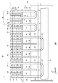
- the active side gate wiring 131 is provided in the active portion 160. By providing the active side gate wiring 131 in the active portion 160, it is possible to reduce the variation in the wiring length from the gate pad 112 in each region of the semiconductor substrate 10.
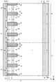
- an N + type cathode region 82 is provided below the buffer region 20.
- the donor concentration in the cathode region 82 is higher than the donor concentration in the drift region 18.
- the donor of the cathode region 82 is, for example, hydrogen or phosphorus.
- the elements that serve as donors and acceptors in each region are not limited to the above-mentioned examples.
- the collector region 22 and the cathode region 82 are exposed on the lower surface 23 of the semiconductor substrate 10 and are connected to the collector electrode 24.
- the collector electrode 24 may come into contact with the entire lower surface 23 of the semiconductor substrate 10.
- the emitter electrode 52 and the collector electrode 24 are made of a metal material such as aluminum.
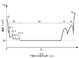
- a part of the buffer area 20 of this example is arranged on the upper surface 21 side of the semiconductor substrate 10.
- the plurality of concentration peaks 25 at least the deepest peak is arranged on the upper surface 21 side.
- the remaining concentration peak 25 is arranged on the lower surface 23 side of the semiconductor substrate 10 as in the example of FIG.
- the doping concentration at the center Zc in the depth direction of the semiconductor substrate 10 is defined as Dc.
- the central Zc is contained in the high concentration region 128.
- the doping concentration Dc is higher than the bulk doping concentration Db.
- the peak value of the doping concentration of the low concentration peak in this example may be 50 times or less, 20 times or less, 10 times or less, or 8 times or less of the doping concentration Dc. It may be 5 times or less, 3 times or less, or 2 times or less.
- the average value of the peak values of the doping concentrations of the concentration peaks 25-5 and the concentration peaks 25-4 may be 50 times or less, 20 times or less, and 10 times or less the doping concentration Dc. It may be 8 times or less, 5 times or less, 3 times or less, or 2 times or less.
Landscapes
- Metal-Oxide And Bipolar Metal-Oxide Semiconductor Integrated Circuits (AREA)
- Insulated Gate Type Field-Effect Transistor (AREA)
Abstract
Priority Applications (5)
| Application Number | Priority Date | Filing Date | Title |
|---|---|---|---|
| DE112020000333.7T DE112020000333T5 (de) | 2019-08-09 | 2020-08-04 | Halbleitervorrichtung |
| JP2021539227A JP7268743B2 (ja) | 2019-08-09 | 2020-08-04 | 半導体装置 |
| CN202080011718.4A CN113454789B (zh) | 2019-08-09 | 2020-08-04 | 半导体装置 |
| US17/385,974 US12191358B2 (en) | 2019-08-09 | 2021-07-27 | Semiconductor device |
| US19/010,128 US20250133795A1 (en) | 2019-08-09 | 2025-01-05 | Semiconductor device |
Applications Claiming Priority (2)
| Application Number | Priority Date | Filing Date | Title |
|---|---|---|---|
| JP2019147450 | 2019-08-09 | ||
| JP2019-147450 | 2019-08-09 |
Related Child Applications (1)
| Application Number | Title | Priority Date | Filing Date |
|---|---|---|---|
| US17/385,974 Continuation US12191358B2 (en) | 2019-08-09 | 2021-07-27 | Semiconductor device |
Publications (1)
| Publication Number | Publication Date |
|---|---|
| WO2021029285A1 true WO2021029285A1 (fr) | 2021-02-18 |
Family
ID=74569591
Family Applications (1)
| Application Number | Title | Priority Date | Filing Date |
|---|---|---|---|
| PCT/JP2020/029879 Ceased WO2021029285A1 (fr) | 2019-08-09 | 2020-08-04 | Dispositif à semi-conducteur |
Country Status (5)
| Country | Link |
|---|---|
| US (2) | US12191358B2 (fr) |
| JP (1) | JP7268743B2 (fr) |
| CN (1) | CN113454789B (fr) |
| DE (1) | DE112020000333T5 (fr) |
| WO (1) | WO2021029285A1 (fr) |
Cited By (3)
| Publication number | Priority date | Publication date | Assignee | Title |
|---|---|---|---|---|
| WO2022265061A1 (fr) * | 2021-06-17 | 2022-12-22 | 富士電機株式会社 | Dispositif à semi-conducteur et procédé de production de dispositif à semi-conducteur |
| WO2023042886A1 (fr) * | 2021-09-15 | 2023-03-23 | 富士電機株式会社 | Dispositif à semi-conducteur et procédé de fabrication de dispositif à semi-conducteur |
| JPWO2023176887A1 (fr) * | 2022-03-16 | 2023-09-21 |
Families Citing this family (3)
| Publication number | Priority date | Publication date | Assignee | Title |
|---|---|---|---|---|
| WO2016204227A1 (fr) * | 2015-06-17 | 2016-12-22 | 富士電機株式会社 | Dispositif à semi-conducteur et procédé de fabrication de dispositif à semi-conducteur |
| JP2023120081A (ja) * | 2022-02-17 | 2023-08-29 | 富士電機株式会社 | 半導体装置 |
| CN117374120B (zh) * | 2023-09-28 | 2024-08-16 | 海信家电集团股份有限公司 | 半导体装置 |
Citations (3)
| Publication number | Priority date | Publication date | Assignee | Title |
|---|---|---|---|---|
| US20080001257A1 (en) * | 2006-06-30 | 2008-01-03 | Infineon Technologies Austria Ag | Semiconductor device with a field stop zone |
| JP2018078314A (ja) * | 2009-11-02 | 2018-05-17 | 富士電機株式会社 | 半導体装置 |
| WO2018135448A1 (fr) * | 2017-01-17 | 2018-07-26 | 富士電機株式会社 | Dispositif à semi-conducteur |
Family Cites Families (29)
| Publication number | Priority date | Publication date | Assignee | Title |
|---|---|---|---|---|
| US6482681B1 (en) | 2000-05-05 | 2002-11-19 | International Rectifier Corporation | Hydrogen implant for buffer zone of punch-through non epi IGBT |
| US20080000125A1 (en) | 2006-06-29 | 2008-01-03 | Wen-Kan Chang | Photo Frame Structure |
| JP5150953B2 (ja) | 2008-01-23 | 2013-02-27 | 三菱電機株式会社 | 半導体装置 |
| DE102011113549B4 (de) | 2011-09-15 | 2019-10-17 | Infineon Technologies Ag | Ein Halbleiterbauelement mit einer Feldstoppzone in einem Halbleiterkörper und ein Verfahren zur Herstellung einer Feldstoppzone in einem Halbleiterkörper |
| CN104054178B (zh) | 2012-03-30 | 2017-09-08 | 富士电机株式会社 | 半导体装置的制造方法 |
| CN104620391B (zh) * | 2012-10-23 | 2017-09-19 | 富士电机株式会社 | 半导体装置及其制造方法 |
| JP6311723B2 (ja) | 2013-12-16 | 2018-04-18 | 富士電機株式会社 | 半導体装置および半導体装置の製造方法 |
| US10211325B2 (en) | 2014-01-28 | 2019-02-19 | Infineon Technologies Ag | Semiconductor device including undulated profile of net doping in a drift zone |
| JP6237921B2 (ja) | 2014-09-30 | 2017-11-29 | 富士電機株式会社 | 半導体装置および半導体装置の製造方法 |
| DE112015006307B4 (de) | 2015-03-13 | 2026-01-15 | Mitsubishi Electric Corporation | Verfahren einer Fertigung einer Halbleitervorrichtung |
| CN107710417B (zh) | 2015-06-16 | 2021-06-11 | 三菱电机株式会社 | 半导体装置的制造方法 |
| CN107004716B (zh) | 2015-06-17 | 2020-12-18 | 富士电机株式会社 | 半导体装置 |
| WO2016204227A1 (fr) | 2015-06-17 | 2016-12-22 | 富士電機株式会社 | Dispositif à semi-conducteur et procédé de fabrication de dispositif à semi-conducteur |
| JP6477897B2 (ja) | 2015-09-16 | 2019-03-06 | 富士電機株式会社 | 半導体装置および半導体装置の製造方法 |
| DE112017000064B4 (de) | 2016-02-23 | 2026-02-05 | Fuji Electric Co., Ltd. | Halbleitervorrichtung |
| JP6508099B2 (ja) | 2016-03-18 | 2019-05-08 | 三菱電機株式会社 | 半導体素子 |
| JP2017188569A (ja) | 2016-04-06 | 2017-10-12 | 三菱電機株式会社 | 半導体装置およびその製造方法 |
| JP6733739B2 (ja) | 2016-10-17 | 2020-08-05 | 富士電機株式会社 | 半導体装置 |
| JP6784148B2 (ja) | 2016-11-10 | 2020-11-11 | 三菱電機株式会社 | 半導体装置、絶縁ゲート型バイポーラトランジスタ、絶縁ゲート型バイポーラトランジスタの製造方法 |
| WO2018092788A1 (fr) * | 2016-11-16 | 2018-05-24 | 富士電機株式会社 | Dispositif à semiconducteur |
| JP6820738B2 (ja) | 2016-12-27 | 2021-01-27 | 三菱電機株式会社 | 半導体装置、電力変換装置および半導体装置の製造方法 |
| US20200273970A1 (en) | 2017-05-10 | 2020-08-27 | Mitsubishi Electric Corporation | Semiconductor device |
| JP6661575B2 (ja) | 2017-06-20 | 2020-03-11 | 三菱電機株式会社 | 半導体装置およびその製造方法 |
| DE112018003666B4 (de) | 2017-07-19 | 2025-02-06 | Mitsubishi Electric Corporation | Verfahren zur herstellung eines halbleiterbauelements und halbleiterbauelement |
| JP6824135B2 (ja) | 2017-09-29 | 2021-02-03 | 三菱電機株式会社 | 半導体装置及びその製造方法 |
| JP7126361B2 (ja) | 2018-03-08 | 2022-08-26 | 三菱電機株式会社 | 半導体装置、電力変換装置、及び、半導体装置の製造方法 |
| JP6964566B2 (ja) | 2018-08-17 | 2021-11-10 | 三菱電機株式会社 | 半導体装置およびその製造方法 |
| JP6702467B2 (ja) | 2019-02-25 | 2020-06-03 | 三菱電機株式会社 | 半導体装置及びその製造方法 |
| JP2020182009A (ja) | 2020-08-12 | 2020-11-05 | 三菱電機株式会社 | 半導体装置およびその製造方法 |
-
2020
- 2020-08-04 WO PCT/JP2020/029879 patent/WO2021029285A1/fr not_active Ceased
- 2020-08-04 CN CN202080011718.4A patent/CN113454789B/zh active Active
- 2020-08-04 JP JP2021539227A patent/JP7268743B2/ja active Active
- 2020-08-04 DE DE112020000333.7T patent/DE112020000333T5/de active Pending
-
2021
- 2021-07-27 US US17/385,974 patent/US12191358B2/en active Active
-
2025
- 2025-01-05 US US19/010,128 patent/US20250133795A1/en active Pending
Patent Citations (3)
| Publication number | Priority date | Publication date | Assignee | Title |
|---|---|---|---|---|
| US20080001257A1 (en) * | 2006-06-30 | 2008-01-03 | Infineon Technologies Austria Ag | Semiconductor device with a field stop zone |
| JP2018078314A (ja) * | 2009-11-02 | 2018-05-17 | 富士電機株式会社 | 半導体装置 |
| WO2018135448A1 (fr) * | 2017-01-17 | 2018-07-26 | 富士電機株式会社 | Dispositif à semi-conducteur |
Cited By (11)
| Publication number | Priority date | Publication date | Assignee | Title |
|---|---|---|---|---|
| WO2022265061A1 (fr) * | 2021-06-17 | 2022-12-22 | 富士電機株式会社 | Dispositif à semi-conducteur et procédé de production de dispositif à semi-conducteur |
| JPWO2022265061A1 (fr) * | 2021-06-17 | 2022-12-22 | ||
| JP7670132B2 (ja) | 2021-06-17 | 2025-04-30 | 富士電機株式会社 | 半導体装置および半導体装置の製造方法 |
| WO2023042886A1 (fr) * | 2021-09-15 | 2023-03-23 | 富士電機株式会社 | Dispositif à semi-conducteur et procédé de fabrication de dispositif à semi-conducteur |
| JPWO2023042886A1 (fr) * | 2021-09-15 | 2023-03-23 | ||
| JP7597233B2 (ja) | 2021-09-15 | 2024-12-10 | 富士電機株式会社 | 半導体装置および半導体装置の製造方法 |
| JP2025027046A (ja) * | 2021-09-15 | 2025-02-26 | 富士電機株式会社 | 半導体装置および半導体装置の製造方法 |
| JP7750364B2 (ja) | 2021-09-15 | 2025-10-07 | 富士電機株式会社 | 半導体装置および半導体装置の製造方法 |
| JPWO2023176887A1 (fr) * | 2022-03-16 | 2023-09-21 | ||
| WO2023176887A1 (fr) * | 2022-03-16 | 2023-09-21 | 富士電機株式会社 | Dispositif à semi-conducteur et procédé de fabrication d'un dispositif à semi-conducteur |
| JP7677531B2 (ja) | 2022-03-16 | 2025-05-15 | 富士電機株式会社 | 半導体装置および半導体装置の製造方法 |
Also Published As
| Publication number | Publication date |
|---|---|
| CN113454789B (zh) | 2025-10-03 |
| JPWO2021029285A1 (ja) | 2021-12-02 |
| US12191358B2 (en) | 2025-01-07 |
| CN113454789A (zh) | 2021-09-28 |
| US20250133795A1 (en) | 2025-04-24 |
| US20210359088A1 (en) | 2021-11-18 |
| DE112020000333T5 (de) | 2021-09-16 |
| JP7268743B2 (ja) | 2023-05-08 |
Similar Documents
| Publication | Publication Date | Title |
|---|---|---|
| JP2021182614A (ja) | 半導体装置および半導体装置の製造方法 | |
| JP7268743B2 (ja) | 半導体装置 | |
| JPWO2019181852A1 (ja) | 半導体装置および半導体装置の製造方法 | |
| JP7272454B2 (ja) | 半導体装置および半導体装置の製造方法 | |
| JP6989061B2 (ja) | 半導体装置および製造方法 | |
| WO2023063411A1 (fr) | Dispositif à semi-conducteurs | |
| US12543355B2 (en) | Semiconductor device | |
| WO2022158053A1 (fr) | Dispositif à semi-conducteurs | |
| WO2023063412A1 (fr) | Dispositif à semi-conducteurs et procédé de fabrication de dispositif à semi-conducteurs | |
| WO2022196768A1 (fr) | Dispositif semi-conducteur | |
| JP7323049B2 (ja) | 半導体装置および半導体装置を備えた電力変換装置 | |
| JP2023170200A (ja) | 半導体装置 | |
| WO2022102711A1 (fr) | Appareil à semi-conducteur et procédé de fabrication d'appareil à semi-conducteur | |
| WO2021166980A1 (fr) | Dispositif semi-conducteur | |
| WO2021145397A1 (fr) | Dispositif semi-conducteur et procédé de fabrication de dispositif semi-conducteur | |
| JPWO2020217683A1 (ja) | 半導体装置および製造方法 | |
| WO2023224059A1 (fr) | Dispositif à semi-conducteur | |
| CN117650157A (zh) | 半导体装置 | |
| WO2023145805A1 (fr) | Dispositif à semi-conducteur et procédé de fabrication | |
| JP2024067536A (ja) | 半導体装置 | |
| WO2022014624A1 (fr) | Dispositif semi-conducteur | |
| JP7683287B2 (ja) | 半導体装置および製造方法 | |
| WO2026049049A1 (fr) | Dispositif à semi-conducteur | |
| WO2025105372A1 (fr) | Dispositif à semi-conducteur et procédé de fabrication de dispositif à semi-conducteur | |
| WO2025164685A1 (fr) | Dispositif à semi-conducteur |
Legal Events
| Date | Code | Title | Description |
|---|---|---|---|
| 121 | Ep: the epo has been informed by wipo that ep was designated in this application |
Ref document number: 20852825 Country of ref document: EP Kind code of ref document: A1 |
|
| ENP | Entry into the national phase |
Ref document number: 2021539227 Country of ref document: JP Kind code of ref document: A |
|
| 122 | Ep: pct application non-entry in european phase |
Ref document number: 20852825 Country of ref document: EP Kind code of ref document: A1 |
|
| WWG | Wipo information: grant in national office |
Ref document number: 202080011718.4 Country of ref document: CN |